Embed Size (px)
Citation preview

Product
Folder
Sample &Buy
Technical
Documents
Tools &
Software
Support &Community
MSP430FR2033, MSP430FR2032SLASE45B –OCTOBER 2014–REVISED AUGUST 2015
MSP430FR203x Mixed-Signal Microcontrollers1 Device Overview
1.1 Features1
• Embedded Microcontroller • Clock System (CS)– 16-Bit RISC Architecture up to 16 MHz – On-Chip 32-kHz RC Oscillator (REFO)– Wide Supply Voltage Range From 1.8 V to – On-Chip 16-MHz Digitally Controlled Oscillator
3.6 V (DCO) With Frequency Locked Loop (FLL)• Optimized Low-Power Modes (at 3 V) • ±1% Accuracy With On-Chip Reference at
Room Temperature– Active: 126 µA/MHz– On-Chip Very Low-Frequency 10-kHz Oscillator– Standby
(VLO)• LPM3.5 With VLO: 0.4 µA– On-Chip High-Frequency Modulation Oscillator• Real-Time Clock (RTC) Counter (LPM3.5
(MODOSC)With 32768-Hz Crystal): 0.77 µA– External 32-kHz Crystal Oscillator (XT1)– Shutdown (LPM4.5): 15 nA– Programmable MCLK Prescalar of 1 to 128• Low-Power Ferroelectric RAM (FRAM)– SMCLK Derived From MCLK With– Up to 15.5KB of Nonvolatile Memory
Programmable Prescalar of 1, 2, 4, or 8– Built-In Error Correction Code (ECC)• General Input/Output and Pin Functionality– Configurable Write Protection
– Total 60 I/Os on 64-Pin Package– Unified Memory of Program, Constants, and– 16 Interrupt Pins (P1 and P2) Can Wake upStorage
MCU From LPMs– 1015 Write Cycle Endurance– All I/Os are Capacitive Touch I/Os– Radiation Resistant and Nonmagnetic
• Development Tools and Software• Intelligent Digital Peripherals– Free Professional Development Environments– IR Modulation Logic
• Family Members (Also See Section 3)– Two 16-Bit Timers With Three Capture/Compare– MSP430FR2033: 15KB of Program FRAM +Registers Each (Timer_A3)
512B of Information FRAM + 2KB of RAM– One 16-Bit Counter-Only RTC Counter– MSP430FR2032: 8KB of Program FRAM +– 16-Bit Cyclic Redundancy Check (CRC) 512B of Information FRAM + 1KB of RAM
• Enhanced Serial Communications • Package Options– Enhanced USCI A (eUSCI_A) Supports UART, – 64 Pin: LQFP (PM)IrDA, and SPI
– 56 Pin: TSSOP (G56)– Enhanced USCI B (eUSCI_B) Supports SPI and– 48 Pin: TSSOP (G48)I2C
• For Complete Module Descriptions, See the• High-Performance AnalogMSP430FR4xx and MSP430FR2xx Family User's– 10-Channel 10-Bit Analog-to-Digital Converter Guide (SLAU445)(ADC)
• Internal 1.5-V Reference• Sample-and-Hold 200 ksps
1.2 Applications• Smoke or Fire Detectors • Temperature Sensors or Controllers• Glass Breakage Detectors • Data Storage, Data Integration• Industrial Sensor Management • Human Machine Interface (HMI) Controllers• System Supervisor, Low-Power Coprocessors
1
An IMPORTANT NOTICE at the end of this data sheet addresses availability, warranty, changes, use in safety-critical applications,intellectual property matters and other important disclaimers. PRODUCTION DATA.

MSP430FR2033, MSP430FR2032SLASE45B –OCTOBER 2014–REVISED AUGUST 2015 www.ti.com
1.3 DescriptionThe TI MSP430™ family of low-power microcontrollers consists of several devices that feature differentsets of peripherals targeted for various applications. The architecture, combined with extensive low-powermodes, is optimized to achieve extended battery life in portable measurement applications. The devicefeatures a powerful 16-bit RISC CPU, 16-bit registers, and constant generators that contribute tomaximum code efficiency. The DCO allows the device to wake up from low-power modes to active modein less than 10 µs.
Device Information (1)
PART NUMBER PACKAGE BODY SIZE (2)
MSP430FR2033IPM LQFP (64) 10 mm × 10 mmMSP430FR2033IG56 TSSOP (56) 14.0 mm × 6.1 mmMSP430FR2033IG48 TSSOP (48) 12.5 mm × 6.1 mmMSP430FR2032IPM LQFP (64) 10 mm × 10 mmMSP430FR2032IG56 TSSOP (56) 14.0 mm × 6.1 mmMSP430FR2032IG48 TSSOP (48) 12.5 mm × 6.1 mm
(1) For the most current part, package, and ordering information, see the Package Option Addendum inSection 9, or see the TI website at www.ti.com.
(2) The sizes shown here are approximations. For the package dimensions with tolerances, see theMechanical Data in Section 9.
2 Device Overview Copyright © 2014–2015, Texas Instruments IncorporatedSubmit Documentation Feedback
Product Folder Links: MSP430FR2033 MSP430FR2032

Capacitive Touch I/O
DVCC
RST/NMI
XIN XOUT P3.x/P4.x P5.x/P6.xP1.x/P2.x P7.x/P8.x
LPM3.5 DomainSBWTDIOSBWTCK
TDOTDI/TCLK
TMSTCK
DVSS
I/O PortsP1/P2
2×8 IOsInterrupt
& WakeupPA
1×16 IOs
ADC
Up to 10-chSingle-end
10-bit200ksps
ClockSystemControl
XT1FRAM
15KB+512B8KB+ B512
RAM
2KB1KB
Watchdog
SYS
TA1
Timer_A3 CC
Registers
eUSCI_A0
(UART,IrDA, SPI)
eUSCI_B0
(SPI, I2C)
CRC16
16-bitCyclic
RedundancyCheck
RTCCounter
16-bitReal-Time
Clock
JTAG
SBW
I/O PortsP3/P4
2×8 IOs
PB1×16 IOs
I/O PortsP5/P6
2×8 IOs
PC1×16 IOs
I/O PortsP7/P8
1×8 IOs
PD1×12 IOs
1×4 IOs
TA0
Timer_A3 CC
Registers
EEM
MAB
MDB
16-MHZ CPUinc.
16 Registers
PowerManagement
Module
MSP430FR2033, MSP430FR2032www.ti.com SLASE45B –OCTOBER 2014–REVISED AUGUST 2015
1.4 Functional Block DiagramFigure 1-1 shows the functional block diagram.
Figure 1-1. Functional Block Diagram• The device has one main power pair of DVCC and DVSS that supplies both digital and analog
modules. Recommended bypass and decouple capacitors are 4.7 µF to 10 µF and 0.1 µF,respectively, with ±5% accuracy.
• P1 and P2 feature the pin-interrupt function and can wake the MCU from LPM3.5.• Each Timer_A3 has three CC registers, but only the CCR1 and CCR2 are externally connected. CCR0
registers can only be used for internal period timing and interrupt generation.• In LPM3.5, the RTC counter can be functional while the remaining peripherals are off.• Not all I/Os are bonded in TSSOP-56 and TSSOP-48 packages (refer to Table 4-1). All I/Os can be
configured as Capacitive Touch I/Os.
Copyright © 2014–2015, Texas Instruments Incorporated Device Overview 3Submit Documentation Feedback
Product Folder Links: MSP430FR2033 MSP430FR2032

MSP430FR2033, MSP430FR2032SLASE45B –OCTOBER 2014–REVISED AUGUST 2015 www.ti.com
Table of Contents1 Device Overview ......................................... 1 5.11 Thermal Characteristics ............................. 17
1.1 Features .............................................. 1 5.12 Timing and Switching Characteristics ............... 181.2 Applications........................................... 1 6 Detailed Description ................................... 321.3 Description............................................ 2 6.1 CPU ................................................. 321.4 Functional Block Diagram ............................ 3 6.2 Operating Modes.................................... 32
2 Revision History ......................................... 4 6.3 Interrupt Vector Addresses.......................... 333 Device Comparison ..................................... 5 6.4 Bootstrap Loader (BSL) ............................. 344 Terminal Configuration and Functions.............. 6 6.5 JTAG Standard Interface............................ 34
4.1 Pin Diagrams ......................................... 6 6.6 Spy-Bi-Wire Interface (SBW)........................ 354.2 Signal Descriptions ................................... 9 6.7 FRAM................................................ 354.3 Pin Multiplexing ..................................... 12 6.8 Memory Protection .................................. 354.4 Connection of Unused Pins ......................... 12 6.9 Peripherals .......................................... 36
5 Specifications ........................................... 13 6.10 Device Descriptors (TLV) ........................... 605.1 Absolute Maximum Ratings ......................... 13 6.11 Memory.............................................. 615.2 ESD Ratings ........................................ 13 6.12 Identification ......................................... 685.3 Recommended Operating Conditions............... 13 7 Applications, Implementation, and Layout........ 695.4 Active Mode Supply Current Into VCC Excluding 7.1 Device Connection and Layout Fundamentals...... 69
External Current..................................... 14 7.2 Peripheral- and Interface-Specific Design5.5 Active Mode Supply Current Per MHz .............. 14 Information .......................................... 725.6 Low-Power Mode LPM0 Supply Currents Into VCC 8 Device and Documentation Support ............... 74
Excluding External Current.......................... 14 8.1 Device Support ...................................... 745.7 Low-Power Mode LPM3, LPM4 Supply Currents 8.2 Documentation Support ............................. 76
(Into VCC) Excluding External Current .............. 158.3 Trademarks.......................................... 775.8 Low-Power Mode LPMx.5 Supply Currents (Into8.4 Electrostatic Discharge Caution..................... 77VCC) Excluding External Current .................... 158.5 Glossary ............................................. 775.9 Typical Characteristics, Low-Power Mode Supply
Currents ............................................. 16 9 Mechanical Packaging and OrderableInformation .............................................. 785.10 Typical Characteristics - Current Consumption Per
Module .............................................. 17 9.1 Packaging Information .............................. 78
2 Revision History
Changes from November 1, 2014 to August 14, 2015 Page
• Corrected "10-BIT ADC CHANNELS" column for MSP430FR2032IPM in Table 3-1, Device Comparison .............. 5• Added Tstg MIN and MAX values.................................................................................................. 13• Added Section 5.2, ESD Ratings.................................................................................................. 13• Changed all graphs in Section 5.9, Typical Characteristics, Low-Power Mode Supply Currents, for new
measurements ...................................................................................................................... 16• Added VREF, 1.2V parameter to Table 5-1, PMM, SVS and BOR ............................................................... 18• Changed tSTE,LEAD MIN value at 2 V from 40 ns to 50 ns ...................................................................... 26• Changed tSTE,LEAD MIN value at 3 V from 24 ns to 45 ns ...................................................................... 26• Changed tVALID,SO MAX value at 2 V from 55 ns to 65 ns ...................................................................... 26• Changed tVALID,SO MAX value at 3 V from 30 ns to 40 ns ...................................................................... 26• Changed fADCOSC TYP value from 4.5 MHz to 5.0 MHz ........................................................................ 29• In Table 6-1, Operating Modes, changed the entry for "Power Consumption at 25°C, 3 V" in AM from
100 µA/MHz to 126 µA/MHz ....................................................................................................... 32• In Table 6-1, Operating Modes, added "with RTC only" to the entry for "Power Consumption at 25°C, 3 V" in
LPM3.5 ............................................................................................................................... 32• In Table 6-2, Interrupt Sources, Flags, and Vectors, removed "FRAM access time error" (ACCTEIFG) from the
"System NMI" row .................................................................................................................. 33
4 Revision History Copyright © 2014–2015, Texas Instruments IncorporatedSubmit Documentation Feedback
Product Folder Links: MSP430FR2033 MSP430FR2032

MSP430FR2033, MSP430FR2032www.ti.com SLASE45B –OCTOBER 2014–REVISED AUGUST 2015
3 Device Comparison
Table 3-1 summarizes the features of the available family members.
Table 3-1. Device Comparison (1) (2)
PROGRAMFRAM + SRAM 10-BIT ADC PACKAGEDEVICE TA0, TA1 eUSCI_A eUSCI_B I/OINFORMATION (BYTES) CHANNELS TYPE
FRAM (BYTES)PMMSP430FR2033IPM 15360 + 512 2048 3 × CCR (3) 1 1 10 60 (LQFP64)G56MSP430FR2033IG56 15360 + 512 2048 3 × CCR (3) 1 1 8 52 (TSSOP56)G48MSP430FR2033IG48 15360 + 512 2048 3 × CCR (3) 1 1 8 44 (TSSOP48)PMMSP430FR2032IPM 8192 + 512 1024 3 × CCR (3) 1 1 10 60 (LQFP64)G56MSP430FR2032IG56 8192 + 512 1024 3 × CCR (3) 1 1 8 52 (TSSOP56)G48MSP430FR2032IG48 8192 + 512 1024 3 × CCR (3) 1 1 8 44 (TSSOP48)
(1) For the most current device, package, and ordering information, see the Package Option Addendum in Section 9, or see the TI websiteat www.ti.com.
(2) Package drawings, standard packing quantities, thermal data, symbolization, and PCB design guidelines are available atwww.ti.com/packaging.
(3) A CCR register is a configurable register that provides internal and external capture or compare inputs, or internal and external PWMoutputs.
Copyright © 2014–2015, Texas Instruments Incorporated Device Comparison 5Submit Documentation Feedback
Product Folder Links: MSP430FR2033 MSP430FR2032

P4.7
P4.6
P4.5
P4.4
P4.3
P4.2/XOUT
P4.1/XIN
DVSS
DVCC
RST/NMI/SBWTDIO
TEST/SBWTCK
P4.0/TA1.1
P8.3/TA1.2
P8.2/TA1CLK
P8.1/ACLK/A9
P8.0/SMCLK/A8
P1.7
/TA
0.1
/TD
O/A
7
P1.6
/TA
0.2
/TD
I/T
CLK
/A6
P1.5
/TA
0C
LK
/TM
S/A
5
P1.4
/MC
LK
/TC
K/A
4/V
RE
F+
P1.3
/UC
A0S
TE
/A3
P1.2
/UC
A0C
LK
/A2
P1.1
//A
1/
UC
A0R
XD
/UC
A0S
OM
IV
ere
f+
P1.0
//A
0/V
ere
f–U
CA
0T
XD
/UC
A0S
IMO
P5.7
P5.6
P5.5
P5.4
P5.3
/UC
B0S
OM
I/U
CB
0S
CL
P5.2
/UC
B0S
IMO
/UC
B0S
DA
P5.1
/UC
B0C
LK
P5.0
/UC
B0S
TE
P2.7
P2.6
P2.5
P2.4
P2.3
P2.2
P2.1
P2.0
P6.7
P6.6
P6.5
P6.4
P6.3
P6.2
P6.1
P6.0
P3.7
P3.6
P3.5
P3.4
P3.3
P3.2
P3.1
P3.0
P7.7
P7.6
P7.5
P7.4
P7.3
P7.2
P7.1
P7.0
1
2
3
4
5
6
7
8
9
10
11
12
13
14
15
16
17
18
19
20
21
22
23
24
25
26
27
28
29
30
31
32
33
34
35
36
37
38
39
40
41
42
43
44
45
46
47
48
49
50
51
52
53
54
55
56
57
58
59
60
61
62
63
64
MSP430FR2033, MSP430FR2032SLASE45B –OCTOBER 2014–REVISED AUGUST 2015 www.ti.com
4 Terminal Configuration and Functions
4.1 Pin DiagramsFigure 4-1 shows the 64-pin PM package.
Figure 4-1. 64-Pin PM (LQFP) Designation (Top View)
6 Terminal Configuration and Functions Copyright © 2014–2015, Texas Instruments IncorporatedSubmit Documentation Feedback
Product Folder Links: MSP430FR2033 MSP430FR2032

P6.543
P6.444
P6.345
P6.246
P6.147
P6.048
P3.749
P3.650
P3.551
P3.452
P3.353
P3.254
P3.155
P3.056
DVCC 15
RST/NMI/SBWTDIO 16
TEST/SBWTCK 17
P4.0/TA1.1 18
P8.3/TA1.2 19
P8.2/TA1CLK 20
P1.7/TA0.1/TDO/A7 21
P1.6/TA0.2/TDI/TCLK/A6 22
P1.5/TA0CLK/TMS/A5 23
P1.4/ /TCK/A4/VREF+MCLK 24
P1.3/UCA0STE/A3 25
P1.2/ /A2UCA0CLK 26
P1.1/ /A1/Veref+UCA0RXD/UCA0SOMI 27
P1.0/ /A0/Veref–UCA0TXD/UCA0SIMO 28
P4.7 7
P4.6 8
P4.5 9
P4.4 10
P4.3 11
P4.2/XOUT 12
P4.1/XIN 13
DVSS 14
P5.529
P5.430
P5.3/UCB0SOMI/UCB0SCL31
P5.2/UCB0SIMO/UCB0SDA32
P5.1/UCB0CLK33
P5.0/UCB0STE34
P2.735
P2.636
P2.537
P2.438
P2.339
P2.240
P2.141
P2.042
P7.5 1
P7.4 2
P7.3 3
P7.2 4
P7.1 5
P7.0 6
MSP430FR2033, MSP430FR2032www.ti.com SLASE45B –OCTOBER 2014–REVISED AUGUST 2015
Figure 4-2 shows the 56-pin G56 package.
Figure 4-2. 56-Pin DGG (TSSOP) Designation (Top View)
Copyright © 2014–2015, Texas Instruments Incorporated Terminal Configuration and Functions 7Submit Documentation Feedback
Product Folder Links: MSP430FR2033 MSP430FR2032

P2.1
35
P2.0
36
P6.3
37
P6.2
38
P6.1
39
P6.0
40
P3.7
41
P3.6
42
P3.5
43
P3.4
44
P3.3
45
P3.2
46
P3.1
47P3.0
48
TEST/SBWTCK
15
P4.0/TA1.1
16
P1.7/TA0.1/TDO/A7
17
P1.6/TA0.2/TDI/TCLK/A6
18
P1.5/TA0CLK/TMS/A5
19
20
P1.3/UCA0STE/A3
21
P1.2/UCA0CLK/A2
22
P1.1/UCA0RXD/UCA0SOMI/A1/Veref+
23 P1.0/UCA0TXD/UCA0SIMO/A0/Veref–
24
P4.5
7
P4.4
8
P4.3
9
P4.2/XOUT
10
P4.1/XIN
11
DVSS
12
DVCC
13
RST/NMI/SBWTDIO
14
P5.3/UCB0SOMI/UCB0SCL
25
P5.2/UCB0SIMO/UCB0SDA
26
P5.1/UCB0CLK
27
P5.0/UCB0STE
28
P2.7
29
P2.6
30
P2.5
31
P2.4
32
P2.3
33
P2.2
34
P7.3
1
P7.2
2
P7.1
3
P7.0
4
P4.7
5
P4.6
6
P1.4/MCLK/TCK/A4/VREF+
MSP430FR2033, MSP430FR2032SLASE45B –OCTOBER 2014–REVISED AUGUST 2015 www.ti.com
Figure 4-3 shows the 48-pin G48 package.
Figure 4-3. 48-Pin DGG (TSSOP) Designation (Top View)
8 Terminal Configuration and Functions Copyright © 2014–2015, Texas Instruments IncorporatedSubmit Documentation Feedback
Product Folder Links: MSP430FR2033 MSP430FR2032

MSP430FR2033, MSP430FR2032www.ti.com SLASE45B –OCTOBER 2014–REVISED AUGUST 2015
4.2 Signal DescriptionsTable 4-1 describes the signals for all device variants and package options.
Table 4-1. Signal Descriptions
TERMINALPACKAGE SUFFIX I/O DESCRIPTION
NAMEPM G56 G48
P4.7 1 7 7 I/O General-purpose I/OP4.6 2 8 8 I/O General-purpose I/OP4.5 3 9 9 I/O General-purpose I/OP4.4 4 10 10 I/O General-purpose I/OP4.3 5 11 11 I/O General-purpose I/O
General-purpose I/OP4.2/XOUT 6 12 12 I/O
Output terminal for crystal oscillatorGeneral-purpose I/O
P4.1/XIN 7 13 13 I/OInput terminal for crystal oscillator
DVSS 8 14 14 Power groundDVCC 9 15 15 Power supply
Reset input active low
RST/NMI/SBWTDIO 10 16 16 I/O Nonmaskable interrupt input
Spy-Bi-Wire data input/outputTest Mode pin – selected digital I/O on JTAG pins
TEST/SBWTCK 11 17 17 ISpy-Bi-Wire input clockGeneral-purpose I/O
P4.0/TA1.1 12 18 18 I/OTimer TA1 CCR1 capture: CCI1A input, compare: Out1 outputsGeneral-purpose I/O
P8.3/TA1.2 (1) 13 19 I/OTimer TA1 CCR2 capture: CCI2A input, compare: Out2 outputsGeneral-purpose I/O
P8.2/TA1CLK (1) 14 20 I/OTimer clock input TACLK for TA1General-purpose I/O
P8.1/ACLK/A9 (1) 15 I/O ACLK output
Analog input A9General-purpose I/O
P8.0/SMCLK/A8 (1) 16 I/O SMCLK output
Analog input A8General-purpose I/O (2)
Timer TA0 CCR1 capture: CCI1A input, compare: Out1 outputsP1.7/TA0.1/TDO/A7 (2) 17 21 19 I/O
Test data output
Analog input A7General-purpose I/O (2)
Timer TA0 CCR2 capture: CCI2A input, compare: Out2 outputsP1.6/TA0.2/TDI/TCLK/A6 (2) 18 22 20 I/O
Test data input or test clock input
Analog input A6
(1) Any pin that is not bonded out in a smaller package must be initialized by software after reset to achieve the lowest leakage current.(2) Because this pin is multiplexed with the JTAG function, TI recommends disabling the pin interrupt function while in JTAG debug to
prevent collisions.
Copyright © 2014–2015, Texas Instruments Incorporated Terminal Configuration and Functions 9Submit Documentation Feedback
Product Folder Links: MSP430FR2033 MSP430FR2032

MSP430FR2033, MSP430FR2032SLASE45B –OCTOBER 2014–REVISED AUGUST 2015 www.ti.com
Table 4-1. Signal Descriptions (continued)TERMINAL
PACKAGE SUFFIX I/O DESCRIPTIONNAME
PM G56 G48General-purpose I/O (2)
Timer clock input TACLK for TA0P1.5/TA0CLK/TMS/A5 (2) 19 23 21 I/O
Test mode select
Analog input A5General-purpose I/O (2)
MCLK output
P1.4/MCLK/TCK/A4/VREF+ (2) 20 24 22 I/O Test clock
Analog input A4
Output of positive reference voltage with ground as referenceGeneral-purpose I/O
P1.3/UCA0STE/A3 21 25 23 I/O eUSCI_A0 SPI slave transmit enable
Analog input A3General-purpose I/O
P1.2/UCA0CLK/A2 22 26 24 I/O eUSCI_A0 SPI clock input/output
Analog input A2General-purpose I/O
eUSCI_A0 UART receive dataP1.1/UCA0RXD/UCA0SOMI/ 23 27 25 I/OA1/Veref+ eUSCI_A0 SPI slave out/master in
Analog input A1, and ADC positive referenceGeneral-purpose I/O
eUSCI_A0 UART transmit dataP1.0/UCA0TXD/UCA0SIMO/ 24 28 26 I/OA0/Veref- eUSCI_A0 SPI slave in/master out
Analog input A0, and ADC negative referenceP5.7 (1) 25 I/O General-purpose I/OP5.6 (1) 26 I/O General-purpose I/OP5.5 (1) 27 29 I/O General-purpose I/OP5.4 (1) 28 30 I/O General-purpose I/O
General-purpose I/OP5.3/UCB0SOMI/UCB0SCL 29 31 27 I/O
eUSCI_B0 SPI slave out/master in; eUSCI_B0 I2C clockGeneral-purpose I/O
P5.2/UCB0SIMO/UCB0SDA 30 32 28 I/OeUSCI_B0 SPI slave in/master out; eUSCI_B0 I2C dataGeneral-purpose I/O
P5.1/UCB0CLK 31 33 29 I/OeUSCI_B0 clock input/outputGeneral-purpose I/O
P5.0/UCB0STE 32 34 30 I/OeUSCI_B0 slave transmit enable
P2.7 33 35 31 I/O General-purpose I/OP2.6 34 36 32 I/O General-purpose I/OP2.5 35 37 33 I/O General-purpose I/OP2.4 36 38 34 I/O General-purpose I/OP2.3 37 39 35 I/O General-purpose I/OP2.2 38 40 36 I/O General-purpose I/OP2.1 39 41 37 I/O General-purpose I/O
10 Terminal Configuration and Functions Copyright © 2014–2015, Texas Instruments IncorporatedSubmit Documentation Feedback
Product Folder Links: MSP430FR2033 MSP430FR2032

MSP430FR2033, MSP430FR2032www.ti.com SLASE45B –OCTOBER 2014–REVISED AUGUST 2015
Table 4-1. Signal Descriptions (continued)TERMINAL
PACKAGE SUFFIX I/O DESCRIPTIONNAME
PM G56 G48P2.0 40 42 38 I/O General-purpose I/OP6.7 (1) 41 I/O General-purpose I/OP6.6 (1) 42 I/O General-purpose I/OP6.5 (1) 43 43 I/O General-purpose I/OP6.4 (1) 44 44 I/O General-purpose I/OP6.3 45 45 39 I/O General-purpose I/OP6.2 46 46 40 I/O General-purpose I/OP6.1 47 47 41 I/O General-purpose I/OP6.0 48 48 42 I/O General-purpose I/OP3.7 49 49 43 I/O General-purpose I/OP3.6 50 50 44 I/O General-purpose I/OP3.5 51 51 45 I/O General-purpose I/OP3.4 52 52 46 I/O General-purpose I/OP3.3 53 53 47 I/O General-purpose I/OP3.2 54 54 48 I/O General-purpose I/OP3.1 55 55 1 I/O General-purpose I/OP3.0 56 56 2 I/O General-purpose I/OP7.7 (1) 57 I/O General-purpose I/OP7.6 (1) 58 I/O General-purpose I/OP7.5 (1) 59 1 I/O General-purpose I/OP7.4 (1) 60 2 I/O General-purpose I/OP7.3 61 3 3 I/O General-purpose I/OP7.2 62 4 4 I/O General-purpose I/OP7.1 63 5 5 I/O General-purpose I/OP7.0 64 6 6 I/O General-purpose I/O
Copyright © 2014–2015, Texas Instruments Incorporated Terminal Configuration and Functions 11Submit Documentation Feedback
Product Folder Links: MSP430FR2033 MSP430FR2032

MSP430FR2033, MSP430FR2032SLASE45B –OCTOBER 2014–REVISED AUGUST 2015 www.ti.com
4.3 Pin MultiplexingPin multiplexing for these devices is controlled by both register settings and operating modes (forexample, if the device is in test mode). For details of the settings for each pin and schematics of themultiplexed ports, see Section 6.9.12.
4.4 Connection of Unused PinsTable 4-2 shows the correct termination of unused pins.
Table 4-2. Connection of Unused Pins (1)
PIN POTENTIAL COMMENTPx.0 to Px.7 Open Set to port function, output direction (PxDIR.n = 1)
RST/NMI DVCC 47-kΩ pullup or internal pullup selected with 10-nF (or 1.1-nF) pulldown (2)
TEST Open This pin always has an internal pulldown enabled.
(1) Any unused pin with a secondary function that is shared with general-purpose I/O should follow the Px.0 to Px.7 unused pin connectionguidelines.
(2) The pulldown capacitor should not exceed 1.1 nF when using devices with Spy-Bi-Wire interface in Spy-Bi-Wire mode with TI tools likeFET interfaces or GANG programmers.
12 Terminal Configuration and Functions Copyright © 2014–2015, Texas Instruments IncorporatedSubmit Documentation Feedback
Product Folder Links: MSP430FR2033 MSP430FR2032

MSP430FR2033, MSP430FR2032www.ti.com SLASE45B –OCTOBER 2014–REVISED AUGUST 2015
5 Specifications
5.1 Absolute Maximum Ratings (1)
over operating free-air temperature range (unless otherwise noted)MIN MAX UNIT
Voltage applied at DVCC pin to VSS –0.3 4.1 VVCC + 0.3Voltage applied to any pin (2) –0.3 V(4.1 Maximum)
Diode current at any device pin ±2 mAMaximum junction temperature, TJ 85 °CStorage temperature, Tstg
(3) –40 125 °C
(1) Stresses beyond those listed under Absolute Maximum Ratings may cause permanent damage to the device. These are stress ratingsonly, and functional operation of the device at these or any other conditions beyond those indicated under Recommended OperatingConditions is not implied. Exposure to absolute-maximum-rated conditions for extended periods may affect device reliability.
(2) All voltages referenced to VSS.(3) Higher temperature may be applied during board soldering according to the current JEDEC J-STD-020 specification with peak reflow
temperatures not higher than classified on the device label on the shipping boxes or reels.
5.2 ESD RatingsVALUE UNIT
Human-body model (HBM), per ANSI/ESDA/JEDEC JS-001 (1) ±1000V(ESD) Electrostatic discharge V
Charged-device model (CDM), per JEDEC specification JESD22-C101 (2) ±250
(1) JEDEC document JEP155 states that 500-V HBM allows safe manufacturing with a standard ESD control process. Pins listed as±1000 V may actually have higher performance.
(2) JEDEC document JEP157 states that 250-V CDM allows safe manufacturing with a standard ESD control process. Pins listed as ±250 Vmay actually have higher performance.
5.3 Recommended Operating ConditionsTypical values are specified at VCC = 3.3 V and TA = 25°C (unless otherwise noted)
MIN NOM MAX UNITVCC Supply voltage applied at DVCC pin (1) (2) (3) 1.8 3.6 VVSS Supply voltage applied at DVSS pin 0 VTA Operating free-air temperature –40 85 °CTJ Operating junction temperature –40 85 °CCDVCC Recommended capacitor at DVCC (4) 4.7 10 µF
No FRAM wait states 0 8(NWAITSx = 0)fSYSTEM Processor frequency (maximum MCLK frequency) (3) (5) MHz
With FRAM wait states 0 16 (7)(NWAITSx = 1) (6)
fACLK Maximum ACLK frequency 40 kHzfSMCLK Maximum SMCLK frequency 16 (7) MHz
(1) Supply voltage changes faster than 0.2 V/µs can trigger a BOR reset even within the recommended supply voltage range.(2) Modules may have a different supply voltage range specification. See the specification of the respective module in this data sheet.(3) The minimum supply voltage is defined by the SVS levels. Refer to the SVS threshold parameters in Table 5-1.(4) A capacitor tolerance of ±20% or better is required.(5) Modules may have a different maximum input clock specification. See the specification of the respective module in this data sheet.(6) Wait states only occur on actual FRAM accesses (that is, on FRAM cache misses). RAM and peripheral accesses are always executed
without wait states.(7) If clock sources such as HF crystals or the DCO with frequencies >16 MHz are used, the clock must be divided in the clock system to
comply with this operating condition.
Copyright © 2014–2015, Texas Instruments Incorporated Specifications 13Submit Documentation Feedback
Product Folder Links: MSP430FR2033 MSP430FR2032

MSP430FR2033, MSP430FR2032SLASE45B –OCTOBER 2014–REVISED AUGUST 2015 www.ti.com
5.4 Active Mode Supply Current Into VCC Excluding External Current (1)
FREQUENCY (fMCLK = fSMCLK)1 MHz 8 MHz 16 MHzEXECUTION TESTPARAMETER 0 WAIT STATES 0 WAIT STATES 1 WAIT STATE UNITMEMORY CONDITIONS (NWAITSx = 0) (NWAITSx = 0) (NWAITSx = 1)
TYP MAX TYP MAX TYP MAX3 V, 25°C 504 2874 3156 3700FRAMIAM, FRAM(0%) µA0% cache hit ratio 3 V, 85°C 516 2919 32053 V, 25°C 209 633 1056 1298FRAMIAM, FRAM(100%) µA100% cache hit ratio 3 V, 85°C 217 647 1074
IAM, RAM(2) RAM 3 V, 25°C 231 809 1450 µA
(1) All inputs are tied to 0 V or to VCC. Outputs do not source or sink any current. Characterized with program executing typical dataprocessing.fACLK = 32786 Hz, fMCLK = fSMCLK = fDCO at specified frequencyProgram and data entirely reside in FRAM. All execution is from FRAM.
(2) Program and data reside entirely in RAM. All execution is from RAM. No access to FRAM.
5.5 Active Mode Supply Current Per MHzVCC = 3 V, TA = 25°C (unless otherwise noted)
PARAMETER TEST CONDITIONS TYP UNIT((IAM, 75% cache hit rate at 8 MHz) –Active mode current consumption per MHz,dIAM,FRAM/df (IAM, 75% cache hit rate at 1 MHz)) 126 µA/MHzexecution from FRAM, no wait states (1)/ 7 MHz
(1) All peripherals are turned on in default settings.
5.6 Low-Power Mode LPM0 Supply Currents Into VCC Excluding External CurrentVCC = 3 V, TA = 25°C (unless otherwise noted) (1) (2)
FREQUENCY (fSMCLK)PARAMETER VCC 1 MHz 8 MHz 16 MHz UNIT
TYP MAX TYP MAX TYP MAX2 V 158 307 415
ILPM0 Low-power mode LPM0 supply current µA3 V 169 318 427
(1) All inputs are tied to 0 V or to VCC. Outputs do not source or sink any current.(2) Current for watchdog timer clocked by SMCLK included.
fACLK = 32786 Hz, fMCLK = 0 MHz, fSMCLK at specified frequency.
14 Specifications Copyright © 2014–2015, Texas Instruments IncorporatedSubmit Documentation Feedback
Product Folder Links: MSP430FR2033 MSP430FR2032

MSP430FR2033, MSP430FR2032www.ti.com SLASE45B –OCTOBER 2014–REVISED AUGUST 2015
5.7 Low-Power Mode LPM3, LPM4 Supply Currents (Into VCC) Excluding External Currentover recommended ranges of supply voltage and operating free-air temperature (unless otherwise noted) (1)
–40°C 25°C 85°CPARAMETER VCC UNIT
TYP MAX TYP MAX TYP MAX3 V 1.13 1.31 1.99 3.00
ILPM3,XT1 Low-power mode 3, includes SVS (2) (3) (4) µA2 V 1.06 1.21 2.943 V 0.92 1.00 1.75 2.89
ILPM3,VLO Low-power mode 3, VLO, excludes SVS (5) µA2 V 0.86 1.00 2.75
ILPM3, RTC Low-power mode 3, RTC, excludes SVS (6) 3 V 1.08 1.25 3.04 µA3 V 0.65 0.75 1.88
ILPM4, SVS Low-power mode 4, includes SVS µA2 V 0.63 0.73 1.853 V 0.51 0.58 1.51
ILPM4 Low-power mode 4, excludes SVS µA2 V 0.50 0.57 1.49
(1) All inputs are tied to 0 V or to VCC. Outputs do not source or sink any current(2) Not applicable for devices with HF crystal oscillator only.(3) Characterized with a GOLLEDGE MS1V-TK/I_32.768KHZ crystal with a load capacitance chosen to closely match the required load.(4) Low-power mode 3, includes SVS test conditions:
Current for watchdog timer clocked by ACLK and RTC clocked by XT1 included. Current for brownout and SVS included (SVSHE = 1).CPUOFF = 1, SCG0 = 1 SCG1 = 1, OSCOFF = 0 (LPM3),fXT1 = 32768 Hz, fACLK = fXT1, fMCLK = fSMCLK = 0 MHz
(5) Low-power mode 3, VLO, excludes SVS test conditions:Current for watchdog timer clocked by VLO included. RTC disabled. Current for brownout included. SVS disabled (SVSHE = 0).CPUOFF = 1, SCG0 = 1 SCG1 = 1, OSCOFF = 0 (LPM3),fXT1 = 0 Hz, fACLK = fMCLK = fSMCLK = 0 MHz
(6) RTC periodically wakes up every second with external 32768-Hz as source.
5.8 Low-Power Mode LPMx.5 Supply Currents (Into VCC) Excluding External Currentover recommended ranges of supply voltage and operating free-air temperature (unless otherwise noted)
–40°C 25°C 85°CPARAMETER VCC UNIT
TYP MAX TYP MAX TYP MAX3 V 0.71 0.77 1.25 1.06 2.06Low-power mode 3.5, includes SVS (1) (2) (3)
ILPM3.5, XT1 µA(also see Figure 5-2) 2 V 0.66 0.70 0.953 V 0.23 0.25 0.375 0.32 0.43
ILPM4.5, SVS Low-power mode 4.5, includes SVS (4) µA2 V 0.20 0.20 0.243 V 0.010 0.015 0.070 0.073 0.140
ILPM4.5 Low-power mode 4.5, excludes SVS (5) µA2 V 0.008 0.013 0.060
(1) Not applicable for devices with HF crystal oscillator only.(2) Characterized with a Micro Crystal MS1V-T1K crystal with a load capacitance chosen to closely match the required load.(3) Low-power mode 3.5, includes SVS test conditions:
Current for RTC clocked by XT1 included. Current for brownout and SVS included (SVSHE = 1). Core regulator disabled.PMMREGOFF = 1, CPUOFF = 1, SCG0 = 1 SCG1 = 1, OSCOFF = 1 (LPMx.5),fXT1 = 32768 Hz, fACLK = fXT1, fMCLK = fSMCLK = 0 MHz
(4) Low-power mode 4.5, includes SVS test conditions:Current for brownout and SVS included (SVSHE = 1). Core regulator disabled.PMMREGOFF = 1, CPUOFF = 1, SCG0 = 1 SCG1 = 1, OSCOFF = 1 (LPMx.5),fXT1 = 0 Hz, fACLK = fMCLK = fSMCLK = 0 MHz
(5) Low-power mode 4.5, excludes SVS test conditions:Current for brownout included. SVS disabled (SVSHE = 0). Core regulator disabled.PMMREGOFF = 1, CPUOFF = 1, SCG0 = 1 SCG1 = 1, OSCOFF = 1 (LPMx.5),fXT1 = 0 Hz, fACLK = fMCLK = fSMCLK = 0 MHz
Copyright © 2014–2015, Texas Instruments Incorporated Specifications 15Submit Documentation Feedback
Product Folder Links: MSP430FR2033 MSP430FR2032

0
0.05
0.1
0.15
0.2
0.25
0.3
0.35
0.4
0.45
0.5
-40 -30 -20 -10 0 10 20 30 40 50 60 70 80
LP
M4
.5 S
up
ply
Cu
rre
nt
(µA
)
Temperature (°C)
0
0.5
1
1.5
2
2.5
3
3.5
4
4.5
5
-40 -30 -20 -10 0 10 20 30 40 50 60 70 80
LP
M3 S
up
ply
Cu
rre
nt
(µA
)
Temperature (°C)
0
0.5
1
1.5
2
2.5
3
-40 -30 -20 -10 0 10 20 30 40 50 60 70 80
LP
M3
.5 S
up
ply
Cu
rre
nt
(µA
)
Temperature (°C)
MSP430FR2033, MSP430FR2032SLASE45B –OCTOBER 2014–REVISED AUGUST 2015 www.ti.com
5.9 Typical Characteristics, Low-Power Mode Supply Currents
LPM3 DVCC = 3 V LPM3.5 DVCC = 3 VSVS disabled RTC counter on 12.5-pF crystal on XT1 SVS enabled
Figure 5-1. LPM3 Supply Current vs Temperature Figure 5-2. LPM3.5 Supply Current vs Temperature
LPM4.5 DVCC = 3 V SVS enabled
Figure 5-3. LPM4.5 Supply Current vs Temperature
16 Specifications Copyright © 2014–2015, Texas Instruments IncorporatedSubmit Documentation Feedback
Product Folder Links: MSP430FR2033 MSP430FR2032

MSP430FR2033, MSP430FR2032www.ti.com SLASE45B –OCTOBER 2014–REVISED AUGUST 2015
5.10 Typical Characteristics - Current Consumption Per ModuleMODULE TEST CONDITIONS REFERENCE CLOCK TYP UNIT
Timer_A Module input clock 5 µA/MHzeUSCI_A UART mode Module input clock 7 µA/MHzeUSCI_A SPI mode Module input clock 5 µA/MHzeUSCI_B SPI mode Module input clock 5 µA/MHzeUSCI_B I2C mode, 100 kbaud Module input clock 5 µA/MHzRTC 32 kHz 85 nACRC From start to end of operation MCLK 8.5 µA/MHz
5.11 Thermal CharacteristicsPARAMETERS VALUE UNIT
θJA Junction-to-ambient thermal resistance, still air (1) 61.7 °C/WθJC, (TOP) Junction-to-case (top) thermal resistance (2) 25.4 °C/WθJB Junction-to-board thermal resistance (3) LQFP-64 (PM) 32.7 °C/WΨJB Junction-to-board thermal characterization parameter 32.4 °C/WΨJT Junction-to-top thermal characterization parameter 2.5 °C/WθJA Junction-to-ambient thermal resistance, still air( (1) 62.4 °C/WθJC, (TOP) Junction-to-case (top) thermal resistance (2) 18.7 °C/WθJB Junction-to-board thermal resistance (3) TSSOP-56 (DGG56) 31.4 °C/WΨJB Junction-to-board thermal characterization parameter 31.1 °C/WΨJT Junction-to-top thermal characterization parameter 0.8 °C/WθJA Junction-to-ambient thermal resistance, still air( (1) 68.9 °C.WθJC, (TOP) Junction-to-case (top) thermal resistance (2) 23 °C/WθJB Junction-to-board thermal resistance (3) TSSOP-48 (DGG48) 35.8 °C/WΨJB Junction-to-board thermal characterization parameter 35.3 °C/WΨJT Junction-to-top thermal characterization parameter 1.1 °C/W
(1) The junction-to-ambient thermal resistance under natural convection is obtained in a simulation on a JEDEC-standard, High-K board, asspecified in JESD51-7, in an environment described in JESD51-2a.
(2) The junction-to-case (top) thermal resistance is obtained by simulating a cold place test on the package top. No specific JEDEC-standard test exists, but a close description can be found in the ANSI SEMI standard G30-88.
(3) The junction-to-board thermal resistance is obtained by simulating in an environment with a ring cold place fixture to control the PCBtemperature, as described in JESD51-8.
Copyright © 2014–2015, Texas Instruments Incorporated Specifications 17Submit Documentation Feedback
Product Folder Links: MSP430FR2033 MSP430FR2032

VBOR
VSVS–VSVS+
t
V
Power Cycle Reset SVS Reset BOR Reset
tBOR
MSP430FR2033, MSP430FR2032SLASE45B –OCTOBER 2014–REVISED AUGUST 2015 www.ti.com
5.12 Timing and Switching Characteristics
5.12.1 Power Supply Sequencing
Figure 5-4. Power Cycle, SVS, and BOR Reset Conditions
Table 5-1. PMM, SVS and BORover recommended ranges of supply voltage and operating free-air temperature (unless otherwise noted)
PARAMETER TEST CONDITIONS MIN TYP MAX UNITVBOR, safe Safe BOR power-down level (1) 0.1 VtBOR, safe Safe BOR reset delay (2) 10 msISVSH,AM SVSH current consumption, active mode VCC = 3.6 V 1.5 µAISVSH,LPM SVSH current consumption, low-power modes VCC = 3.6 V 240 nAVSVSH- SVSH power-down level 1.71 1.81 1.87 VVSVSH+ SVSH power-up level 1.76 1.88 1.99 VVSVSH_hys SVSH hysteresis 70 mVtPD,SVSH, AM SVSH propagation delay, active mode 10 µstPD,SVSH, LPM SVSH propagation delay, low-power modes 100 µsVREF, 1.2V 1.2-V REF voltage (3) 1.158 1.200 1.242 V
(1) A safe BOR can be correctly generated only if DVCC drops below this voltage before it rises.(2) When an BOR occurs, a safe BOR can be correctly generated only if DVCC is kept low longer than this period before it reaches VSVSH+.(3) This is a characterized result with external 1-mA load to ground from –40°C to +85°C.
18 Specifications Copyright © 2014–2015, Texas Instruments IncorporatedSubmit Documentation Feedback
Product Folder Links: MSP430FR2033 MSP430FR2032

MSP430FR2033, MSP430FR2032www.ti.com SLASE45B –OCTOBER 2014–REVISED AUGUST 2015
5.12.2 Reset Timing
Table 5-2. Wake-Up Times From Low-Power Modes and Resetover recommended ranges of supply voltage and operating free-air temperature (unless otherwise noted)
TESTPARAMETER VCC MIN TYP MAX UNITCONDITIONSAdditional wake-up time to activate the FRAM inAM if previously disabled by the FRAM controller ortWAKE-UP FRAM 3 V 10 µsfrom a LPM if immediate activation is selected forwakeup (1)
200 ns +tWAKE-UP LPM0 Wake-up time from LPM0 to active mode (1) 3V 2.5/fDCO
tWAKE-UP LPM3 Wake-up time from LPM3 to active mode (2) 3 V 10 µstWAKE-UP LPM4 Wake-up time from LPM4 to active mode 3 V 10 µstWAKE-UP LPM3.5 Wake-up time from LPM3.5 to active mode (2) 3 V 350 µs
SVSHE = 1 3 V 350 µstWAKE-UP LPM4.5 Wake-up time from LPM4.5 to active mode (2)
SVSHE = 0 3 V 1 msWake-up time from RST or BOR event to activetWAKE-UP-RESET 3 V 1 msmode (2)
Pulse duration required at RST/NMI pin to accept atRESET 3 V 2 µsreset
(1) The wake-up time is measured from the edge of an external wake-up signal (for example, port interrupt or wake-up event) to the firstexternally observable MCLK clock edge.
(2) The wake-up time is measured from the edge of an external wake-up signal (for example, port interrupt or wake-up event) until the firstinstruction of the user program is executed.
Copyright © 2014–2015, Texas Instruments Incorporated Specifications 19Submit Documentation Feedback
Product Folder Links: MSP430FR2033 MSP430FR2032

MSP430FR2033, MSP430FR2032SLASE45B –OCTOBER 2014–REVISED AUGUST 2015 www.ti.com
5.12.3 Clock Specifications
Table 5-3. XT1 Crystal Oscillator (Low Frequency)over recommended ranges of supply voltage and operating free-air temperature (unless otherwise noted) (1)
PARAMETER TEST CONDITIONS VCC MIN TYP MAX UNITXT1 oscillator crystal, lowfXT1, LF LFXTBYPASS = 0 32768 Hzfrequency
Measured at MCLK,DCXT1, LF XT1 oscillator LF duty cycle 30% 70%fLFXT = 32768 HzXT1 oscillator logic-level square-fXT1,SW LFXTBYPASS = 1 (2) (3) 32768 Hzwave input frequencyLFXT oscillator logic-level square-DCXT1, SW LFXTBYPASS = 1 40% 60%wave input duty cycleOscillation allowance for LFXTBYPASS = 0, LFXTDRIVE = 3,OALFXT 200 kΩLF crystals (4) fLFXT = 32768 Hz, CL,eff = 12.5 pFIntegrated effective loadCL,eff See (6) 1 pFcapacitance (5)
fOSC = 32768 HztSTART,LFXT Start-up time (7) LFXTBYPASS = 0, LFXTDRIVE = 3, 1000 ms
TA = 25°C, CL,eff = 12.5 pFfFault,LFXT Oscillator fault frequency (8) XTS = 0 (9) 0 3500 Hz
(1) To improve EMI on the LFXT oscillator, the following guidelines should be observed.• Keep the trace between the device and the crystal as short as possible.• Design a good ground plane around the oscillator pins.• Prevent crosstalk from other clock or data lines into oscillator pins XIN and XOUT.• Avoid running PCB traces underneath or adjacent to the XIN and XOUT pins.• Use assembly materials and processes that avoid any parasitic load on the oscillator XIN and XOUT pins.• If conformal coating is used, make sure that it does not induce capacitive or resistive leakage between the oscillator pins.
(2) When LFXTBYPASS is set, LFXT circuits are automatically powered down. Input signal is a digital square wave with parametricsdefined in the Schmitt-trigger inputs section of this data sheet. Duty cycle requirements are defined by DCLFXT, SW.
(3) Maximum frequency of operation of the entire device cannot be exceeded.(4) Oscillation allowance is based on a safety factor of 5 for recommended crystals. The oscillation allowance is a function of the
LFXTDRIVE settings and the effective load. In general, comparable oscillator allowance can be achieved based on the followingguidelines, but should be evaluated based on the actual crystal selected for the application:• For LFXTDRIVE = 0, CL,eff = 3.7 pF.• For LFXTDRIVE = 1, 6 pF ≤ CL,eff ≤ 9 pF.• For LFXTDRIVE = 2, 6 pF ≤ CL,eff ≤ 10 pF.• For LFXTDRIVE = 3, 6 pF ≤ CL,eff ≤ 12 pF.
(5) Includes parasitic bond and package capacitance (approximately 2 pF per pin).(6) Requires external capacitors at both terminals. Values are specified by crystal manufacturers.(7) Includes start-up counter of 1024 clock cycles.(8) Frequencies above the MAX specification do not set the fault flag. Frequencies between the MIN and MAX specification may set the
flag. A static condition or stuck at fault condition sets the flag.(9) Measured with logic-level input frequency but also applies to operation with crystals.
20 Specifications Copyright © 2014–2015, Texas Instruments IncorporatedSubmit Documentation Feedback
Product Folder Links: MSP430FR2033 MSP430FR2032

MSP430FR2033, MSP430FR2032www.ti.com SLASE45B –OCTOBER 2014–REVISED AUGUST 2015
Table 5-4. DCO FLL, Frequencyover recommended operating free-air temperature (unless otherwise noted)
PARAMETER TEST CONDITIONS VCC MIN TYP MAX UNITFLL lock frequency, 16 MHz, 25°C –1.0% 1.0%Measured at MCLK, Internal
trimmed REFO as referenceFLL lock frequency, 16 MHz, –40°C to +85°C –2.0% 2.0%fDCO, FLL 3 VMeasured at MCLK, XT1FLL lock frequency, 16 MHz, –40°C to +85°C –0.5% 0.5%crystal as reference
fDUTY Duty cycle 40% 50% 60%Jittercc Cycle-to-cycle jitter, 16 MHz 0.25%Measured at MCLK, XT1 3 Vcrystal as referenceJitterlong Long-term jitter, 16 MHz 0.022%tFLL, lock FLL lock time 120 ms
Table 5-5. REFOover recommended operating free-air temperature (unless otherwise noted)
PARAMETER TEST CONDITIONS VCC MIN TYP MAX UNITIREFO REFO oscillator current consumption TA = 25°C 3 V 15 µA
REFO calibrated frequency Measured at MCLK 3 V 32768 HzfREFO REFO absolute calibrated tolerance –40°C to +85°C 1.8 V to 3.6 V –3.5% 3.5%dfREFO/dT REFO frequency temperature drift Measured at MCLK (1) 3 V 0.01 %/°CdfREFO/ Measured at MCLK atREFO frequency supply voltage drift 1.8 V to 3.6 V 1 %/VdVCC 25°C (2)
fDC REFO duty cycle Measured at MCLK 1.8 V to 3.6 V 40% 50% 60%tSTART REFO start-up time 40% to 60% duty cycle 50 µs
(1) Calculated using the box method: (MAX(–40°C to 85°C) – MIN(–40°C to 85°C)) / MIN(–40°C to 85°C) / (85°C – (–40°C))(2) Calculated using the box method: (MAX(1.8 V to 3.6 V) – MIN(1.8 V to 3.6 V)) / MIN(1.8 V to 3.6 V) / (3.6 V – 1.8 V)
Table 5-6. Internal Very-Low-Power Low-Frequency Oscillator (VLO)over recommended ranges of supply voltage and operating free-air temperature (unless otherwise noted)
PARAMETER TEST CONDITIONS VCC MIN TYP MAX UNITfVLO VLO frequency Measured at MCLK 3 V 10 kHzdfVLO/dT VLO frequency temperature drift Measured at MCLK (1) 3 V 0.5 %/°CdfVLO/dVCC VLO frequency supply voltage drift Measured at MCLK (2) 1.8 V to 3.6 V 4 %/VfVLO,DC Duty cycle Measured at MCLK 3 V 50%
(1) Calculated using the box method: (MAX(–40°C to 85°C) – MIN(–40°C to 85°C)) / MIN(–40°C to 85°C) / (85°C – (–40°C))(2) Calculated using the box method: (MAX(1.8 V to 3.6 V) – MIN(1.8 V to 3.6 V)) / MIN(1.8 V to 3.6 V) / (3.6 V – 1.8 V)
Table 5-7. Module Oscillator (MODOSC)over recommended ranges of supply voltage and operating free-air temperature (unless otherwise noted)
TESTPARAMETER VCC MIN TYP MAX UNITCONDITIONSfMODOSC MODOSC frequency 3 V 3.8 4.8 5.8 MHzfMODOSC/dT MODOSC frequency temperature drift 3 V 0.102 %/fMODOSC/dVCC MODOSC frequency supply voltage drift 1.8 V to 3.6 V 1.02 %/VfMODOSC,DC Duty cycle 3 V 40% 50% 60%
Copyright © 2014–2015, Texas Instruments Incorporated Specifications 21Submit Documentation Feedback
Product Folder Links: MSP430FR2033 MSP430FR2032

MSP430FR2033, MSP430FR2032SLASE45B –OCTOBER 2014–REVISED AUGUST 2015 www.ti.com
5.12.4 Digital I/Os
Table 5-8. Digital Inputsover recommended ranges of supply voltage and operating free-air temperature (unless otherwise noted)
PARAMETER TEST CONDITIONS VCC MIN TYP MAX UNIT2 V 0.90 1.50
VIT+ Positive-going input threshold voltage V3 V 1.35 2.252 V 0.50 1.10
VIT– Negative-going input threshold voltage V3 V 0.75 1.652 V 0.3 0.8
Vhys Input voltage hysteresis (VIT+ – VIT–) V3 V 0.4 1.2
For pullup: VIN = VSSRPull Pullup or pulldown resistor 20 35 50 kΩFor pulldown: VIN = VCC
CI,dig Input capacitance, digital only port pins VIN = VSS or VCC 3 pFInput capacitance, port pins with shared analogCI,ana VIN = VSS or VCC 5 pFfunctions
Ilkg(Px.y) High-impedance leakage current (1) (2) 2 V, 3 V –20 20 nA
(1) The leakage current is measured with VSS or VCC applied to the corresponding pins, unless otherwise noted.(2) The leakage of the digital port pins is measured individually. The port pin is selected for input and the pullup or pulldown resistor is
disabled.
Table 5-9. Digital Outputsover recommended ranges of supply voltage and operating free-air temperature (unless otherwise noted)
PARAMETER TEST CONDITIONS VCC MIN TYP MAX UNITI(OHmax) = –3 mA (1) 2 V 1.4 2.0
VOH High-level output voltage VI(OHmax) = –5 mA (1) 3 V 2.4 3.0I(OLmax) = 3 mA (1) 2 V 0.0 0.60
VOL Low-level output voltage VI(OHmax) = 5 mA (1) 3 V 0.0 0.60
2 V 16fPort_CLK Clock output frequency CL = 20 pF (2) MHz
3 V 162 V 10
trise,dig Port output rise time, digital only port pins CL = 20 pF ns3 V 72 V 10
tfall,dig Port output fall time, digital only port pins CL = 20 pF ns3 V 5
(1) The maximum total current, I(OHmax) and I(OLmax), for all outputs combined should not exceed ±48 mA to hold the maximum voltage dropspecified.
(2) The port can output frequencies at least up to the specified limit and might support higher frequencies.
22 Specifications Copyright © 2014–2015, Texas Instruments IncorporatedSubmit Documentation Feedback
Product Folder Links: MSP430FR2033 MSP430FR2032

-25
-20
-15
-10
-5
0
0 0.5 1 1.5 2 2.5 3
T = 85°CA
T = 25°CA
High-Level Output Voltage (V)
Hig
h-L
ev
el O
utp
ut
Cu
rre
nt
(mA
)
-10
-7.5
-5
-2.5
0
0 0.25 0.5 0.75 1 1.25 1.5 1.75 2
T = 85°CA
T = 25°CA
High-Level Output Voltage (V)
Hig
h-L
ev
el O
utp
ut
Cu
rre
nt
(mA
)
0
2.5
5
7.5
10
0 0.25 0.5 0.75 1 1.25 1.5 1.75 2
T = 85°CA
T = 25°CA
Low-Level Output Voltage (V)
Lo
w-L
ev
el
Ou
tpu
t C
urr
en
t (m
A)
0
5
10
15
20
25
0 0.5 1 1.5 2 2.5 3
Low-Level Output Voltage (V)
T = 85°CA
T = 25°CA
Lo
w-L
ev
el O
utp
ut
Cu
rre
nt
(mA
)
MSP430FR2033, MSP430FR2032www.ti.com SLASE45B –OCTOBER 2014–REVISED AUGUST 2015
5.12.4.1 Digital I/O Typical Characteristics
Figure 5-5. Typical Low-Level Output Current vs Low-Level Figure 5-6. Typical Low-Level Output Current vs Low-LevelOutput Voltage (DVCC = 3 V) Output Voltage (DVCC = 2 V)
Figure 5-7. Typical High-Level Output Current vs High-Level Figure 5-8. Typical High-Level Output Current vs High-LevelOutput Voltage (DVCC = 3 V) Output Voltage (DVCC = 2 V)
5.12.5 Timer_A
Table 5-10. Timer_A Recommended Operating Conditionsover recommended ranges of supply voltage and operating free-air temperature (unless otherwise noted)
PARAMETER TEST CONDITIONS VCC MIN MAX UNITInternal: SMCLK, ACLK
fTA Timer_A input clock frequency External: TACLK 2 V, 3 V 16 MHzDuty cycle = 50% ±10%
Copyright © 2014–2015, Texas Instruments Incorporated Specifications 23Submit Documentation Feedback
Product Folder Links: MSP430FR2033 MSP430FR2032

MSP430FR2033, MSP430FR2032SLASE45B –OCTOBER 2014–REVISED AUGUST 2015 www.ti.com
5.12.6 eUSCI
Table 5-11. eUSCI (UART Mode) Recommended Operating Conditionsover recommended ranges of supply voltage and operating free-air temperature (unless otherwise noted)
PARAMETER TEST CONDITIONS VCC MIN MAX UNITInternal: SMCLK, MODCLK
feUSCI eUSCI input clock frequency External: UCLK 2 V, 3 V 16 MHzDuty cycle = 50% ±10%
BITCLK clock frequencyfBITCLK 2 V, 3 V 5 MHz(equals baud rate in Mbaud)
Table 5-12. eUSCI (UART Mode) Switching Characteristicsover recommended ranges of supply voltage and operating free-air temperature (unless otherwise noted)
PARAMETER TEST CONDITIONS VCC TYP UNITUCGLITx = 0 12UCGLITx = 1 40
tt UART receive deglitch time (1) 2 V, 3 V nsUCGLITx = 2 68UCGLITx = 3 110
(1) Pulses on the UART receive input (UCxRX) shorter than the UART receive deglitch time are suppressed. To ensure that pulses arecorrectly recognized, their duration should exceed the maximum specification of the deglitch time.
Table 5-13. eUSCI (SPI Master Mode) Recommended Operating Conditionsover recommended ranges of supply voltage and operating free-air temperature (unless otherwise noted)
PARAMETER CONDITIONS MIN MAX UNITInternal: SMCLK, MODCLKfeUSCI eUSCI input clock frequency 8 MHzDuty cycle = 50% ±10%
Table 5-14. eUSCI (SPI Master Mode) Switching Characteristicsover recommended ranges of supply voltage and operating free-air temperature (unless otherwise noted) (1)
PARAMETER TEST CONDITIONS VCC MIN MAX UNITUCxCLKtSTE,LEAD STE lead time, STE active to clock UCSTEM = 1, UCMODEx = 01 or 10 1 cyclesUCxCLKtSTE,LAG STE lag time, Last clock to STE inactive UCSTEM = 1, UCMODEx = 01 or 10 1 cycles
2 V 45tSU,MI SOMI input data setup time ns
3 V 352 V 0
tHD,MI SOMI input data hold time ns3 V 02 V 20UCLK edge to SIMO valid,tVALID,MO SIMO output data valid time (2) nsCL = 20 pF 3 V 202 V 0
tHD,MO SIMO output data hold time (3) CL = 20 pF ns3 V 0
(1) fUCxCLK = 1/2tLO/HI with tLO/HI = max(tVALID,MO(eUSCI) + tSU,SI(Slave), tSU,MI(eUSCI) + tVALID,SO(Slave)).For the slave parameters tSU,SI(Slave) and tVALID,SO(Slave) refer to the SPI parameters of the attached slave.
(2) Specifies the time to drive the next valid data to the SIMO output after the output changing UCLK clock edge. Refer to the timingdiagrams in Figure 5-9 and Figure 5-10.
(3) Specifies how long data on the SIMO output is valid after the output changing UCLK clock edge. Negative values indicate that the dataon the SIMO output can become invalid before the output changing clock edge observed on UCLK. Refer to the timing diagrams inFigure 5-9 and Figure 5-10.
24 Specifications Copyright © 2014–2015, Texas Instruments IncorporatedSubmit Documentation Feedback
Product Folder Links: MSP430FR2033 MSP430FR2032

tSU,MI
tHD,MI
UCLK
SOMI
SIMO
tVALID,MO
CKPL = 0
CKPL = 1
tLOW/HIGH tLOW/HIGH
1/fUCxCLK
tSU,MI
tHD,MI
UCLK
SOMI
SIMO
tVALID,MO
CKPL = 0
CKPL = 1
tLOW/HIGH tLOW/HIGH
1/fUCxCLK
MSP430FR2033, MSP430FR2032www.ti.com SLASE45B –OCTOBER 2014–REVISED AUGUST 2015
Figure 5-9. SPI Master Mode, CKPH = 0
Figure 5-10. SPI Master Mode, CKPH = 1
Copyright © 2014–2015, Texas Instruments Incorporated Specifications 25Submit Documentation Feedback
Product Folder Links: MSP430FR2033 MSP430FR2032

MSP430FR2033, MSP430FR2032SLASE45B –OCTOBER 2014–REVISED AUGUST 2015 www.ti.com
Table 5-15. eUSCI (SPI Slave Mode) Switching Characteristicsover recommended ranges of supply voltage and operating free-air temperature (unless otherwise noted) (1)
PARAMETER TEST CONDITIONS VCC MIN MAX UNIT2 V 55
tSTE,LEAD STE lead time, STE active to clock ns3 V 452 V 20
tSTE,LAG STE lag time, Last clock to STE inactive ns3 V 202 V 65
tSTE,ACC STE access time, STE active to SOMI data out ns3 V 402 V 40STE disable time, STE inactive to SOMI hightSTE,DIS nsimpedance 3 V 352 V 4
tSU,SI SIMO input data setup time ns3 V 42 V 12
tHD,SI SIMO input data hold time ns3 V 122 V 65UCLK edge to SOMI valid,tVALID,SO SOMI output data valid time (2) nsCL = 20 pF 3 V 402 V 5
tHD,SO SOMI output data hold time (3) CL = 20 pF ns3 V 5
(1) fUCxCLK = 1/2tLO/HI with tLO/HI ≥ max(tVALID,MO(Master) + tSU,SI(eUSCI), tSU,MI(Master) + tVALID,SO(eUSCI)).For the master parameters tSU,MI(Master) and tVALID,MO(Master) refer to the SPI parameters of the attached slave.
(2) Specifies the time to drive the next valid data to the SOMI output after the output changing UCLK clock edge. Refer to the timingdiagrams in Figure 5-11 and Figure 5-12.
(3) Specifies how long data on the SOMI output is valid after the output changing UCLK clock edge. Refer to the timing diagrams inFigure 5-11 and Figure 5-12.
26 Specifications Copyright © 2014–2015, Texas Instruments IncorporatedSubmit Documentation Feedback
Product Folder Links: MSP430FR2033 MSP430FR2032

STE
UCLK
CKPL = 0
CKPL = 1
SOMI
SIMO
tSU,SI
tHD,SI
tVALID,SO
tSTE,LEAD
tLOW/HIGH
1/fUCxCLK
tLOW/HIGH
tSTE,LAG
tDIStACC
STE
UCLK
CKPL = 0
CKPL = 1
SOMI
SIMO
tSU,SIMO
tHD,SIMO
tVALID,SOMI
tSTE,LEAD
tLOW/HIGH
1/fUCxCLK
tLOW/HIGH
tSTE,LAG
tDIStACC
MSP430FR2033, MSP430FR2032www.ti.com SLASE45B –OCTOBER 2014–REVISED AUGUST 2015
Figure 5-11. SPI Slave Mode, CKPH = 0
Figure 5-12. SPI Slave Mode, CKPH = 1
Copyright © 2014–2015, Texas Instruments Incorporated Specifications 27Submit Documentation Feedback
Product Folder Links: MSP430FR2033 MSP430FR2032
SDA
SCL
tHD,DAT
tSU,DAT
tHD,STA
tHIGHtLOW
tBUFtHD,STAtSU,STA
tSP
tSU,STO
MSP430FR2033, MSP430FR2032SLASE45B –OCTOBER 2014–REVISED AUGUST 2015 www.ti.com
Table 5-16. eUSCI (I2C Mode) Switching Characteristicsover recommended ranges of supply voltage and operating free-air temperature (unless otherwise noted) (see Figure 5-13)
PARAMETER TEST CONDITIONS VCC MIN TYP MAX UNITInternal: SMCLK, MODCLK
feUSCI eUSCI input clock frequency External: UCLK 16 MHzDuty cycle = 50% ±10%
fSCL SCL clock frequency 2 V, 3 V 0 400 kHzfSCL = 100 kHz 4.0
tHD,STA Hold time (repeated) START 2 V, 3 V µsfSCL > 100 kHz 0.6fSCL = 100 kHz 4.7
tSU,STA Setup time for a repeated START 2 V, 3 V µsfSCL > 100 kHz 0.6
tHD,DAT Data hold time 2 V, 3 V 0 nstSU,DAT Data setup time 2 V, 3 V 250 ns
fSCL = 100 kHz 4.0tSU,STO Setup time for STOP 2 V, 3 V µs
fSCL > 100 kHz 0.6UCGLITx = 0 50 600UCGLITx = 1 25 300Pulse duration of spikes suppressed bytSP 2 V, 3 V nsinput filter UCGLITx = 2 12.5 150UCGLITx = 3 6.3 75UCCLTOx = 1 27
tTIMEOUT Clock low time-out UCCLTOx = 2 2 V, 3 V 30 msUCCLTOx = 3 33
Figure 5-13. I2C Mode Timing
28 Specifications Copyright © 2014–2015, Texas Instruments IncorporatedSubmit Documentation Feedback
Product Folder Links: MSP430FR2033 MSP430FR2032

MSP430FR2033, MSP430FR2032www.ti.com SLASE45B –OCTOBER 2014–REVISED AUGUST 2015
5.12.7 ADC
Table 5-17. ADC, Power Supply and Input Range Conditionsover operating free-air temperature range (unless otherwise noted)
PARAMETER TEST CONDITIONS VCC MIN TYP MAX UNITDVCC ADC supply voltage 2.0 3.6 VV(Ax) Analog input voltage range All ADC pins 0 DVCC V
Operating supply current into 2 V 185fADCCLK = 5 MHz, ADCON = 1,DVCC terminal, referenceIADC REFON = 0, SHT0 = 0, SHT1 = 0, µAcurrent not included, repeat- 3 V 207ADCDIV = 0, ADCCONSEQx = 10bsingle-channel modeOnly one terminal Ax can be selected at one
CI Input capacitance time from the pad to the ADC capacitor array, 2.2 V 1.6 2.0 pFincluding wiring and pad
RI Input MUX ON resistance DVCC = 2 V, 0 V = VAx = DVCC 2 kΩ
Table 5-18. ADC, 10-Bit Timing Parametersover operating free-air temperature range (unless otherwise noted)
PARAMETER TEST CONDITIONS VCC MIN TYP MAX UNITFor specified performance of ADC linearity 2 V tofADCCLK 0.45 5 5.5 MHzparameters 3.6 V
Internal ADC oscillator 2 V tofADCOSC ADCDIV = 0, fADCCLK = fADCOSC 4.5 5.0 5.5 MHz(MODOSC) 3.6 VREFON = 0, Internal oscillator, 2 V to10 ADCCLK cycles, 10-bit mode, 2.18 2.673.6 VfADCOSC = 4.5 MHz to 5.5 MHztCONVERT Conversion time µsExternal fADCCLK from ACLK, MCLK, or SMCLK, 2 V to (1)ADCSSEL ≠ 0 3.6 VThe error in a conversion started after tADCON is lessTurnon settling time oftADCON than ±0.5 LSB, 100 nsthe ADC Reference and input signal already settledRS = 1000 Ω, RI = 36000 Ω, CI = 3.5 pF, 2 V 1.5
tSample Sampling time Approximately eight Tau (t) are required for an error µs3 V 2.0of less than ±0.5 LSB
(1) 12 × ADCDIV × 1/fADCCLK
Copyright © 2014–2015, Texas Instruments Incorporated Specifications 29Submit Documentation Feedback
Product Folder Links: MSP430FR2033 MSP430FR2032

MSP430FR2033, MSP430FR2032SLASE45B –OCTOBER 2014–REVISED AUGUST 2015 www.ti.com
Table 5-19. ADC, 10-Bit Linearity Parametersover operating free-air temperature range (unless otherwise noted)
PARAMETER TEST CONDITIONS VCC MIN TYP MAX UNIT2.4 V toIntegral linearity error (10-bit mode) –2 23.6 V
EI VDVCC as reference LSB2 V toIntegral linearity error (8-bit mode) –2 23.6 V
2.4 V toDifferential linearity error (10-bit mode) –1 13.6 VED VDVCC as reference LSB
2 V toDifferential linearity error (8-bit mode) –1 13.6 V2.4 V toOffset error (10-bit mode) –6.5 6.53.6 V
EO VDVCC as reference mV2 V toOffset error (8-bit mode) –6.5 6.53.6 V
VDVCC as reference –2.0 2.0 LSB2.4 V toGain error (10-bit mode) 3.6 VInternal 1.5-V reference –3.0% 3.0%EG VDVCC as reference –2.0 2.0 LSB2 V toGain error (8-bit mode) 3.6 VInternal 1.5-V reference –3.0% 3.0%
VDVCC as reference –2.0 2.0 LSB2.4 V toTotal unadjusted error (10-bit mode) 3.6 VInternal 1.5-V reference –3.0% 3.0%ET VDVCC as reference –2.0 2.0 LSB2 V toTotal unadjusted error (8-bit mode) 3.6 VInternal 1.5-V reference –3.0% 3.0%VSENSOR See (1) ADCON = 1, INCH = 0Ch, TA = 0°C 3 V 1.013 mVTCSENSOR See (2) ADCON = 1, INCH = 0Ch 3 V 3.35 mV/°C
ADCON = 1, INCH = 0Ch, Error ofconversion result ≤ 1 LSB, AM and all 3 V 30
tSENSOR Sample time required if channel 12 is LPM above LPM3 µs(sample) selected (3)
ADCON = 1, INCH = 0Ch, Error of 3 V 100conversion result ≤ 1 LSB, LPM3
(1) The temperature sensor offset can vary significantly. TI recommends a single-point calibration to minimize the offset error of the built-intemperature sensor.
(2) The device descriptor structure contains calibration values for 30°C ±3°C and 85°C ±3°C for each of the available reference voltagelevels. The sensor voltage can be computed as VSENSE = TCSENSOR × (Temperature, °C) + VSENSOR, where TCSENSOR and VSENSOR canbe computed from the calibration values for higher accuracy.
(3) The typical equivalent impedance of the sensor is 700 kΩ. The sample time required includes the sensor-on time tSENSOR(on).
30 Specifications Copyright © 2014–2015, Texas Instruments IncorporatedSubmit Documentation Feedback
Product Folder Links: MSP430FR2033 MSP430FR2032

MSP430FR2033, MSP430FR2032www.ti.com SLASE45B –OCTOBER 2014–REVISED AUGUST 2015
5.12.8 FRAM
Table 5-20. FRAMover recommended ranges of supply voltage and operating free-air temperature (unless otherwise noted)
PARAMETER TEST CONDITIONS MIN MAX UNITRead and write endurance 1015 cycles
TJ = 25°C 100tRetention Data retention duration TJ = 70°C 40 years
TJ = 85°C 10
5.12.9 Emulation and Debug
Table 5-21. JTAG and Spy-Bi-Wire Interface Characteristicsover recommended ranges of supply voltage and operating free-air temperature (unless otherwise noted)
PARAMETER VCC MIN TYP MAX UNITfSBW Spy-Bi-Wire input frequency 2 V, 3 V 0 10 MHztSBW,Low Spy-Bi-Wire low clock pulse duration 2 V, 3 V 0.028 15 µstSBW, En Spy-Bi-Wire enable time (TEST high to acceptance of first clock edge) (1) 2 V, 3 V 110 µstSBW,Rst Spy-Bi-Wire return to normal operation time 15 100 µs
2 V 0 16fTCK TCK input frequency, 4-wire JTAG (2) MHz
3 V 0 16Rinternal Internal pulldown resistance on TEST 2 V, 3 V 20 35 50 kΩ
(1) Tools that access the Spy-Bi-Wire interface must wait for the tSBW,En time after pulling the TEST/SBWTCK pin high before applying thefirst SBWTCK clock edge.
(2) fTCK may be restricted to meet the timing requirements of the module selected.
Copyright © 2014–2015, Texas Instruments Incorporated Specifications 31Submit Documentation Feedback
Product Folder Links: MSP430FR2033 MSP430FR2032

MSP430FR2033, MSP430FR2032SLASE45B –OCTOBER 2014–REVISED AUGUST 2015 www.ti.com
6 Detailed Description
6.1 CPUThe MSP430 CPU has a 16-bit RISC architecture that is highly transparent to the application. Alloperations, other than program-flow instructions, are performed as register operations in conjunction withseven addressing modes for source operand and four addressing modes for destination operand.
The CPU is integrated with 16 registers that provide reduced instruction execution time. The register-to-register operation execution time is one cycle of the CPU clock.
Four of the registers, R0 to R3, are dedicated as program counter (PC), stack pointer (SP), status register(SR), and constant generator (CG), respectively. The remaining registers are general-purpose registers.
Peripherals are connected to the CPU using data, address, and control buses, and can be handled with allinstructions.
6.2 Operating ModesThe MSP430 has one active mode and several software selectable low-power modes of operation. Aninterrupt event can wake up the device from low-power mode LPM0 or LPM3, service the request, andrestore back to the low-power mode on return from the interrupt program. Low-power modes LPM3.5 andLPM4.5 disable the core supply to minimize power consumption.
Table 6-1. Operating Modes
AM LPM0 LPM3 LPM4 LPM3.5 LPM4.5MODE ACTIVE ONLY RTCCPU OFF STANDBY OFF SHUTDOWNMODE COUNTER
Maximum System Clock 16 MHz 16 MHz 40 kHz 0 40 kHz 00.6 µA 0.77 µA with 13 nAPower Consumption at 25°C, 3 V 126 µA/MHz 20 µA/MHz 1.2 µA without SVS RTC only without SVS
Wake-up time N/A instant 10 µs 10 µs 150 µs 150 µsRTC Counter,Wake-up events N/A All All I/O I/OI/O
Full Full Partial Power Partial Power Partial PowerRegulator Power DownRegulation Regulation Down Down DownPower SVS On On Optional Optional Optional Optional
Brown Out On On On On On OnMCLK Active Off Off Off Off Off
SMCLK Optional Optional Off Off Off OffFLL Optional Optional Off Off Off OffDCO Optional Optional Off Off Off Off
Clock MODCLK Optional Optional Off Off Off OffREFO Optional Optional Optional Off Off OffACLK Optional Optional Optional Off Off Off
XT1CLK Optional Optional Optional Off Optional OffVLOCLK Optional Optional Optional Off Optional Off
CPU On Off Off Off Off OffFRAM On On Off Off Off Off
CoreRAM On On On On Off Off
Backup Memory (1) On On On On On Off
(1) Backup memory contains one 32-byte register in the peripheral memory space. Refer to Table 6-31 and Table 6-49 for its memoryallocation.
32 Detailed Description Copyright © 2014–2015, Texas Instruments IncorporatedSubmit Documentation Feedback
Product Folder Links: MSP430FR2033 MSP430FR2032

MSP430FR2033, MSP430FR2032www.ti.com SLASE45B –OCTOBER 2014–REVISED AUGUST 2015
Table 6-1. Operating Modes (continued)AM LPM0 LPM3 LPM4 LPM3.5 LPM4.5
MODE ACTIVE ONLY RTCCPU OFF STANDBY OFF SHUTDOWNMODE COUNTERTimer0_A3 Optional Optional Optional Off Off OffTimer1_A3 Optional Optional Optional Off Off Off
WDT Optional Optional Optional Off Off OffeUSCI_A0 Optional Optional Off Off Off Off
PeripheralseUSCI_B0 Optional Optional Off Off Off Off
CRC Optional Optional Off Off Off OffADC Optional Optional Optional Off Off Off
RTC Counter Optional Optional Optional Off State Held OffGeneral Digital On Optional State Held State Held Off State HeldInput/OutputI/O
Capacitive Touch I/O Optional Optional Optional Off Off Off
6.3 Interrupt Vector AddressesThe interrupt vectors and the power-up start address are in the address range 0FFFFh to 0FF80h. Thevector contains the 16-bit address of the appropriate interrupt-handler instruction sequence
Table 6-2. Interrupt Sources, Flags, and Vectors
SYSTEM WORDINTERRUPT SOURCE INTERRUPT FLAG PRIORITYINTERRUPT ADDRESSSystem Reset
Power-up, Brownout, Supply Supervisor SVSHIFGExternal Reset RST PMMRSTIFG
Watchdog Time-out, Key Violation WDTIFG Reset FFFEh 63, HighestFRAM uncorrectable bit error detection PMMPORIFG, PMMBORIFG
Software POR, SYSRSTIVFLL unlock error FLLUNLOCKIFG
System NMIVacant Memory Access VMAIFG Nonmaskable FFFCh 62JTAG Mailbox JMBINIFG, JMBOUTIFGFRAM bit error detection CBDIFG, UBDIFG
User NMIExternal NMI NMIIFG Nonmaskable FFFAh 61
Oscillator Fault OFIFGTimer0_A3 TA0CCR0 CCIFG0 Maskable FFF8h 60
TA0CCR1 CCIFG1, TA0CCR2Timer0_A3 Maskable FFF6h 59CCIFG2, TA0IFG (TA0IV)Timer1_A3 TA1CCR0 CCIFG0 Maskable FFF4h 58
TA1CCR1 CCIFG1, TA1CCR2Timer1_A3 Maskable FFF2h 57CCIFG2, TA1IFG (TA1IV)RTC Counter RTCIFG Maskable FFF0h 56
Watchdog Timer Interval mode WDTIFG Maskable FFEEh 55UCTXCPTIFG, UCSTTIFG,
UCRXIFG, UCTXIFG (UARTmode)eUSCI_A0 Receive or Transmit Maskable FFECh 54UCRXIFG, UCTXIFG (SPImode)
(UCA0IV))
Copyright © 2014–2015, Texas Instruments Incorporated Detailed Description 33Submit Documentation Feedback
Product Folder Links: MSP430FR2033 MSP430FR2032

MSP430FR2033, MSP430FR2032SLASE45B –OCTOBER 2014–REVISED AUGUST 2015 www.ti.com
Table 6-2. Interrupt Sources, Flags, and Vectors (continued)SYSTEM WORDINTERRUPT SOURCE INTERRUPT FLAG PRIORITYINTERRUPT ADDRESS
UCB0RXIFG, UCB0TXIFG (SPImode)
UCALIFG, UCNACKIFG,UCSTTIFG, UCSTPIFG,UCRXIFG0, UCTXIFG0,
eUSCI_B0 Receive or Transmit UCRXIFG1, UCTXIFG1, Maskable FFEAh 53UCRXIFG2, UCTXIFG2,UCRXIFG3, UCTXIFG3,
UCCNTIFG, UCBIT9IFG (I2Cmode)
(UCB0IV)ADCIFG0, ADCINIFG,
ADCLOIFG, ADCHIIFG,ADC Maskable FFE8h 52ADCTOVIFG, ADCOVIFG(ADCIV)
P1 P1IFG.0 to P1IFG.7 (P1IV) Maskable FFE6h 51P2 P2IFG.0 to P2IFG.7 (P2IV) Maskable FFE4h 50, Lowest
Reserved Reserved Maskable FFE2h-FF88hBSL Signature 2 0FF86hBSL Signature 1 0FF84h
SignaturesJTAG Signature 2 0FF82hJTAG Signature 1 0FF80h
6.4 Bootstrap Loader (BSL)The BSL enables users to program the FRAM or RAM using a UART serial interface. Access to the devicememory through the BSL is protected by an user-defined password. Use of the BSL requires four pins asshown in Table 6-3. BSL entry requires a specific entry sequence on the RST/NMISBWTDIO andTEST/SBWTCK pins. For a complete description of the features of the BSL and its implementation, seethe MSP430FR4xx and MSP430FR2xx Bootstrap Loader (BSL) User's Guide (SLAU610).
Table 6-3. BSL Pin Requirements and Functions
DEVICE SIGNAL BSL FUNCTIONRST/NMI/SBWTDIO Entry sequence signal
TEST/SBWTCK Entry sequence signalP1.0 Data transmitP1.1 Data receiveVCC Power SupplyVSS Ground Supply
6.5 JTAG Standard InterfaceThe MSP430 family supports the standard JTAG interface which requires four signals for sending andreceiving data. The JTAG signals are shared with general-purpose I/O. The TEST/SBWTCK pin is used toenable the JTAG signals. In addition to these signals, the RST/NMI/SBWTDIO is required to interface withMSP430 development tools and device programmers. The JTAG pin requirements are shown in Table 6-4. For further details on interfacing to development tools and device programmers, see the MSP430Hardware Tools User's Guide (SLAU278). For a complete description of the features of the JTAG interfaceand its implementation, see MSP430 Programming Via the JTAG Interface (SLAU320).
34 Detailed Description Copyright © 2014–2015, Texas Instruments IncorporatedSubmit Documentation Feedback
Product Folder Links: MSP430FR2033 MSP430FR2032

MSP430FR2033, MSP430FR2032www.ti.com SLASE45B –OCTOBER 2014–REVISED AUGUST 2015
Table 6-4. JTAG Pin Requirements and Function
DEVICE SIGNAL DIRECTION JTAG FUNCTIONP1.4/MCLK/TCK/A4/VREF+ IN JTAG clock input
P1.5/TA0CLK/TMS/A5 IN JTAG state controlP1.6/TA0.2/TDI/TCLK/A6 IN JTAG data input/TCLK input
P1.7/TA0.1/TDO/A7 OUT JTAG data outputTEST/SBWTCK IN Enable JTAG pins
RST/NMI/SBWTDIO IN External ResetVCC Power SupplyVSS Ground Supply
6.6 Spy-Bi-Wire Interface (SBW)The MSP430 family supports the 2-wire Spy-Bi-Wire interface. Spy-Bi-Wire can be used to interface withMSP430 development tools and device programmers. Table 6-5 shows the Spy-Bi-Wire interface pinrequirements. For further details on interfacing to development tools and device programmers, refer to theMSP430 Hardware Tools User's Guide (SLAU278).
Table 6-5. Spy-Bi-Wire Pin Requirements and Functions
DEVICE SIGNAL DIRECTION SBW FUNCTIONTEST/SBWTCK IN Spy-Bi-Wire clock input
RST/NMI/SBWTDIO IN, OUT Spy-Bi-Wire data input/outputVCC Power SupplyVSS Ground Supply
6.7 FRAMThe FRAM can be programmed using the JTAG port, Spy-Bi-Wire (SBW), the BSL, or in-system by theCPU. Features of the FRAM include:• Byte and word access capability• Programmable wait state generation• Error correction coding (ECC)
6.8 Memory ProtectionThe device features memory protection that can restrict user access and enable write protection:• Securing the whole memory map to prevent unauthorized access from JTAG port or BSL, by writing
JTAG and BSL signatures using the JTAG port, SBW, the BSL, or in-system by the CPU.• Write protection enabled to prevent unwanted write operation to FRAM contents by setting the control
bits in System Configuration register 0. For more detailed information, refer to the SYS chapter in theMSP430FR4xx and MSP430FR2xx Family User's Guide (SLAU445).
NOTEThe FRAM is protected by default on PUC. To write to FRAM during code execution, theapplication must first clear the corresponding PFWP or DFWP bit in System ConfigurationRegister 0 to unprotect the FRAM.
Copyright © 2014–2015, Texas Instruments Incorporated Detailed Description 35Submit Documentation Feedback
Product Folder Links: MSP430FR2033 MSP430FR2032

MSP430FR2033, MSP430FR2032SLASE45B –OCTOBER 2014–REVISED AUGUST 2015 www.ti.com
6.9 PeripheralsPeripherals are connected to the CPU through data, address, and control buses. All peripherals can behandled by using all instructions in the memory map. For complete module description, see theMSP430FR4xx and MSP430FR2xx Family User's Guide (SLAU445).
6.9.1 Power Management Module (PMM) and On-chip Reference VoltagesThe PMM includes an integrated voltage regulator that supplies the core voltage to the device. The PMMalso includes supply voltage supervisor (SVS) and brownout protection. The brownout reset circuit (BOR)is implemented to provide the proper internal reset signal to the device during power-on and power-off.The SVS circuitry detects if the supply voltage drops below a user-selectable safe level. SVS circuitry isavailable on the primary supply.
The device contains two on-chip reference: 1.5 V for internal reference and 1.2 V for external reference.
The 1.5-V reference is internally connected to ADC channel 13. DVCC is internally connected to ADCchannel 15. When DVCC is set as the reference voltage for ADC conversion, the DVCC can be easilyrepresent as Equation 1 by using ADC sampling 1.5-V reference without any external componentssupport.DVCC = (1023 × 1.5 V) ÷ 1.5-V Reference ADC result (1)
A 1.2-V reference voltage can be buffered and output to P1.4/MCLK/TCK/A4/VREF+, when the ADCchannel 4 is selected as the function. For more detailed information, refer to the MSP430FR4xx andMSP430FR2xx Family User's Guide (SLAU445).
6.9.2 Clock System (CS) and Clock DistributionThe clock system includes a 32-kHz crystal oscillator (XT1), an internal very low-power low-frequencyoscillator (VLO), an integrated 32-kHz RC oscillator (REFO), an integrated internal digitally controlledoscillator (DCO) that may use frequency-locked loop (FLL) locking with internal or external 32-kHzreference clock, and on-chip asynchronous high-speed clock (MODOSC). The clock system is designed totarget cost-effective designs with minimal external components. A fail-safe mechanism is designed forXT1. The clock system module offers the following clock signals.• Main Clock (MCLK): the system clock used by the CPU and all relevant peripherals accessed by the
bus. All clock sources except MODOSC can be selected as the source with a predivider of 1, 2, 4, 8,16, 32, 64, or 128.
• Sub-Main Clock (SMCLK): the subsystem clock used by the peripheral modules. SMCLK derives fromthe MCLK with a predivider of 1, 2, 4, or 8. This means SMCLK is always equal to or less than MCLK.
• Auxiliary Clock (ACLK): this clock is derived from the external XT1 clock or internal REFO clock up to40 kHz.
All peripherals may have one or several clock sources depending on specific functionality. Table 6-6shows the clock distribution used in this device.
36 Detailed Description Copyright © 2014–2015, Texas Instruments IncorporatedSubmit Documentation Feedback
Product Folder Links: MSP430FR2033 MSP430FR2032

MSP430FR2033, MSP430FR2032www.ti.com SLASE45B –OCTOBER 2014–REVISED AUGUST 2015
Table 6-6. Clock Distribution
CLOCKSOURCE MCLK SMCLK ACLK MODCLK XT1CLK (1) VLOCLK EXTERNAL PINSELECT
BITSFrequency DC to DC to DC to DC to 10 kHz5 MHz ±10%Range 16 MHz 16 MHz 40 kHz 40 kHz ±50%CPU N/A DefaultFRAM N/A DefaultRAM N/A DefaultCRC N/A DefaultI/O N/A DefaultTA0 TASSEL 10b 01b 00b (TA0CLK pin)TA1 TASSEL 10b 01b 00b (TA1CLK pin)eUSCI_A0 UCSSEL 10b or 11b 01b 00b (UCA0CLK pin)eUSCI_B0 UCSSEL 10b or 11b 01b 00b (UCB0CLK pin)WDT WDTSSEL 00b 01b 10bADC ADCSSEL 11b 01b 00bRTC RTCSS 01b 10b 11b
(1) To enable XT1 functionality, configure P4SEL0.1 (XIN) and P4SEL0.2 (XOUT) before configuring the Clock System registers.
6.9.3 General-Purpose Input/Output Port (I/O)There are up to 60 I/O ports implemented, depending on the package.• P1, P2, P3, P4, P5, P6, and P7 are full 8-bit ports; P8 has 4 bits implemented.• All individual I/O bits are independently programmable.• Any combination of input, output, and interrupt conditions is possible.• Programmable pullup or pulldown on all ports.• Edge-selectable interrupt and LPM3.5 and LPM4.5 wake-up input capability is available for P1 and P2.• Read and write access to port-control registers is supported by all instructions.• Ports can be accessed byte-wise or word-wise in pairs.• Capacitive Touch I/O functionality is supported on all pins.
NOTEConfiguration of digital I/Os after BOR reset
To prevent any cross currents during start-up of the device, all port pins are high-impedancewith Schmitt triggers and module functions disabled. To enable the I/O functions after a BORreset, the ports must be configured first and then the LOCKLPM5 bit must be cleared. Fordetails, refer to the Configuration After Reset section in the Digital I/O chapter of theMSP430FR4xx and MSP430FR2xx Family User's Guide (SLAU445)
Copyright © 2014–2015, Texas Instruments Incorporated Detailed Description 37Submit Documentation Feedback
Product Folder Links: MSP430FR2033 MSP430FR2032

MSP430FR2033, MSP430FR2032SLASE45B –OCTOBER 2014–REVISED AUGUST 2015 www.ti.com
6.9.4 Watchdog Timer (WDT)The primary function of the WDT module is to perform a controlled system restart after a software problemoccurs. If the selected time interval expires, a system reset is generated. If the watchdog function is notneeded in an application, the module can be configured as interval timer and can generate interrupts atselected time intervals.
Table 6-7. WDT Clocks
NORMAL OPERATIONWDTSSELx (WATCHDOG AND INTERVAL TIMER MODE)00 SMCLK01 ACLK10 VLOCLK11 VLOCLK
6.9.5 System Module (SYS)The SYS module handles many of the system functions within the device. These include Power-On Reset(POR) and Power-Up Clear (PUC) handling, NMI source selection and management, reset interrupt vectorgenerators, bootstrap loader entry mechanisms, and configuration management (device descriptors). SYSalso includes a data exchange mechanism through SBW called a JTAG mailbox mail box that can be usedin the application.
Table 6-8. System Module Interrupt Vector Registers
INTERRUPT VECTOR ADDRESS INTERRUPT EVENT VALUE PRIORITYREGISTERNo interrupt pending 00h
Brownout (BOR) 02h HighestRSTIFG RST/NMI (BOR) 04h
PMMSWBOR software BOR (BOR) 06hLPMx.5 wakeup (BOR) 08hSecurity violation (BOR) 0Ah
Reserved 0ChSVSHIFG SVSH event (BOR) 0Eh
Reserved 10hReserved 12h
SYSRSTIV, System Reset 015EhPMMSWPOR software POR (POR) 14hWDTIFG watchdog time-out (PUC) 16hWDTPW password violation (PUC) 18h
FRCTLPW password violation (PUC) 1AhUncorrectable FRAM bit error detection 1Ch
Peripheral area fetch (PUC) 1EhPMMPW PMM password violation (PUC) 20h
Reserved 22hFLL unlock (PUC) 24h
Reserved 26h to 3Eh Lowest
38 Detailed Description Copyright © 2014–2015, Texas Instruments IncorporatedSubmit Documentation Feedback
Product Folder Links: MSP430FR2033 MSP430FR2032

MSP430FR2033, MSP430FR2032www.ti.com SLASE45B –OCTOBER 2014–REVISED AUGUST 2015
Table 6-8. System Module Interrupt Vector Registers (continued)INTERRUPT VECTOR ADDRESS INTERRUPT EVENT VALUE PRIORITYREGISTER
No interrupt pending 00hSVS low-power reset entry 02h Highest
Uncorrectable FRAM bit error detection 04hReserved 06hReserved 08hReserved 0AhReserved 0Ch
SYSSNIV, System NMI 015ChReserved 0EhReserved 10h
VMAIFG Vacant memory access 12hJMBINIFG JTAG mailbox input 14h
JMBOUTIFG JTAG mailbox output 16hCorrectable FRAM bit error detection 18h
Reserved 1Ah to 1Eh LowestNo interrupt pending 00h
NMIFG NMI pin or SVSH event 02h HighestSYSUNIV, User NMI 015Ah
OFIFG oscillator fault 04hReserved 06h to 1Eh Lowest
6.9.6 Cyclic Redundancy Check (CRC)The 16-bit cyclic redundancy check (CRC) module produces a signature based on a sequence of datavalues and can be used for data checking purposes. The CRC generation polynomial is compliant withCRC-16-CCITT standard of x16 + x12 + x5 + 1.
6.9.7 Enhanced Universal Serial Communication Interface (eUSCI_A0, eUSCI_B0)The eUSCI modules are used for serial data communications. The eUSCI_A module supports eitherUART or SPI communications. The eUSCI_B module supports either SPI or I2C communications.Additionally, eUSCI_A supports automatic baud-rate detection and IrDA.
Table 6-9. eUSCI Pin Configurations
PIN UART SPIP1.0 TXD SIMO
eUSCI_A0 P1.1 RXD SOMIP1.2 SCLKP1.3 STEPIN I2C SPIP5.0 STE
eUSCI_B0 P5.1 SCLKP5.2 SDA SIMOP5.3 SCL SOMI
Copyright © 2014–2015, Texas Instruments Incorporated Detailed Description 39Submit Documentation Feedback
Product Folder Links: MSP430FR2033 MSP430FR2032

MSP430FR2033, MSP430FR2032SLASE45B –OCTOBER 2014–REVISED AUGUST 2015 www.ti.com
6.9.8 Timers (Timer0_A3, Timer1_A3)The Timer0_A3 and Timer1_A3 modules are 16-bit timers and counters with three capture/compareregisters each. Each timer can support multiple captures or compares, PWM outputs, and interval timing.Each timer has extensive interrupt capabilities. Interrupts may be generated from the counter on overflowconditions and from each of the capture/compare registers. The CCR0 registers on both TA0 and TA1 arenot externally connected and can only be used for hardware period timing and interrupt generation. In Upmode, they can be used to set the overflow value of the counter.
Table 6-10. Timer0_A3 Signal Connections
DEVICE INPUT MODULE INPUT MODULE OUTPUT DEVICE OUTPUTPORT PIN MODULE BLOCKSIGNAL NAME SIGNAL SIGNALP1.5 TA0CLK TACLK
ACLK (internal) ACLKTimer N/ASMCLK (internal) SMCLK
From Capacitive INCLKTouch I/O (internal)CCI0A
Timer1_A3 CCI0BCCI0B inputCCR0 TA0DVSS GNDDVCC VCC
P1.7 TA0.1 CCI1A TA0.1Timer1_A3 CCI1BFrom RTC (internal) CCI1B inputCCR1 TA1
DVSS GNDDVCC VCC
P1.6 TA0.2 CCI2A TA0.2Timer1_A3 INCLK
From Capacitive Timer1_A3 CCI2BCCI2BTouch I/O (internal) input,CCR2 TA2IR Input
DVSS GNDDVCC VCC
40 Detailed Description Copyright © 2014–2015, Texas Instruments IncorporatedSubmit Documentation Feedback
Product Folder Links: MSP430FR2033 MSP430FR2032

MSP430FR2033, MSP430FR2032www.ti.com SLASE45B –OCTOBER 2014–REVISED AUGUST 2015
Table 6-11. Timer1_A3 Signal Connections
DEVICE INPUT MODULE INPUT MODULE OUTPUT DEVICE OUTPUTPORT PIN MODULE BLOCKSIGNAL NAME SIGNAL SIGNALP8.2 TA1CLK TACLK
ACLK (internal) ACLKTimer N/ASMCLK (internal) SMCLK
Timer0_A3 CCR2B INCLKoutput (internal)CCI0A
Timer0_A3 CCR0B CCI0Boutput (internal) CCR0 TA0DVSS GNDDVCC VCC
P4.0 TA1.1 CCI1A TA1.1Timer0_A3 CCR1B CCI1B To ADC triggeroutput (internal) CCR1 TA1
DVSS GNDDVCC VCC
P8.3 TA1.2 CCI2A TA1.2Timer0_A3 CCR2B CCI2B IR Inputoutput (internal) CCR2 TA2
DVSS GNDDVCC VCC
The interconnection of Timer0_A3 and Timer1_A3 can be used to modulate the eUSCI_A pin ofUCA0TXD/UCA0SIMO in either ASK or FSK mode. This configuration helps an application easily acquirea modulated infrared command for directly driving an external IR diode.
The IR functions are controlled by the following bits in the System Configuration 1 (SYSCFG1) register:IREN (enable), IRPSEL (polarity select), IRMSEL (mode select), IRDSEL (data select), and IRDATA(data). For more information, refer to the SYS chapter in the MSP430FR4xx and MSP430FR2xx FamilyUser's Guide (SLAU445).
Copyright © 2014–2015, Texas Instruments Incorporated Detailed Description 41Submit Documentation Feedback
Product Folder Links: MSP430FR2033 MSP430FR2032

MSP430FR2033, MSP430FR2032SLASE45B –OCTOBER 2014–REVISED AUGUST 2015 www.ti.com
6.9.9 Real-Time Clock (RTC) CounterThe RTC counter is a 16-bit modulo counter that is functional in AM, LPM0, LPM3, and LPM3.5. The RTCcan periodically wake up the CPU from LPM0, LPM3, or LPM3.5 based on timing from a low-power clocksource such as the XT1 and VLO clocks. In AM, RTC can be driven by SMCLK to generate high-frequency timing events and interrupts. The RTC overflow events trigger:• Timer0_A3 CCR1B• ADC conversion trigger when ADCSHSx bits are set as 01b
6.9.10 10-Bit Analog Digital Converter (ADC)The 10-bit ADC module supports fast 10-bit analog-to-digital conversions with single-ended input. Themodule implements a 10-bit SAR core, sample select control, reference generator and a conversion resultbuffer. A window comparator with a lower and upper limit allows CPU independent result monitoring withthree window comparator interrupt flags.
The ADC supports 10 external inputs and four internal inputs (see Table 6-12).
Table 6-12. ADC Channel Connections
ADCSHSx ADC CHANNELS EXTERNAL PIN OUT0 A0/Veref– P1.01 A1/Veref+ P1.12 A2 P1.23 A3 P1.34 A4 (1) P1.45 A5 P1.56 A6 P1.67 A7 P1.78 A8 P8.0 (2)
9 A9 P8.1 (2)
10 Not used N/A11 Not used N/A12 On-chip temperature sensor N/A13 Reference voltage (1.5 V) N/A14 DVSS N/A15 DVCC N/A
(1) When A4 is used, the PMM 1.2-V reference voltage can be output to this pin by setting the PMMcontrol register. The 1.2-V voltage can be directly measured by A4 channel.
(2) P8.0 and P8.1 are only available in the LQFP-64 package.
The A/D conversion can be started by software or a hardware trigger. Table 6-13 shows the triggersources that are available.
Table 6-13. ADC Trigger Signal Connections
ADCSHSxTRIGGER SOURCE
BINARY DECIMAL00 0 ADCSC bit (software trigger)01 1 RTC event10 2 TA1.1B11 3 TA1.2B
42 Detailed Description Copyright © 2014–2015, Texas Instruments IncorporatedSubmit Documentation Feedback
Product Folder Links: MSP430FR2033 MSP430FR2032

MSP430FR2033, MSP430FR2032www.ti.com SLASE45B –OCTOBER 2014–REVISED AUGUST 2015
6.9.11 Embedded Emulation Module (EEM)The EEM supports real-time in-system debugging. The EEM on these devices has the following features:• Three hardware triggers or breakpoints on memory access• One hardware trigger or breakpoint on CPU register write access• Up to four hardware triggers can be combined to form complex triggers or breakpoints• One cycle counter• Clock control on module level
Copyright © 2014–2015, Texas Instruments Incorporated Detailed Description 43Submit Documentation Feedback
Product Folder Links: MSP430FR2033 MSP430FR2032

0
1
Q
0
1
D
S
EdgeSelect
P1IES.x
P1IFG.x
P1 Interrupt
P1IE.x
P1IN.x
To module
P1SEL0.x
From Module
P1OUT.x
P1DIR.x
From ADC A
A0..A7
0
1From Module
DVCC
DVSS
P1REN.x
EN
D
BusKeeper
P1.0/ /A0P1.1/ /A1P1.2/ /A2P1.3/ /A3P1.4/ /TCK/A4/VREF+P1.5/TA0CLK/TMS/A5P1.6/TA0.2/TDI/TCLK/A6P1.7/TA0.1/TDO/A7
UCA0TXD/UCA0SIMOUCA0RXD/UCA0SOMIUCA0CLKUCA0STEMCLK
From JTAG
To JTAG
MSP430FR2033, MSP430FR2032SLASE45B –OCTOBER 2014–REVISED AUGUST 2015 www.ti.com
6.9.12 Input/Output Schematics
6.9.12.1 Port P1 Input/Output With Schmitt Trigger
Figure 6-1. Port P1 Input/Output With Schmitt Trigger
44 Detailed Description Copyright © 2014–2015, Texas Instruments IncorporatedSubmit Documentation Feedback
Product Folder Links: MSP430FR2033 MSP430FR2032

MSP430FR2033, MSP430FR2032www.ti.com SLASE45B –OCTOBER 2014–REVISED AUGUST 2015
Table 6-14. Port P1 Pin Functions
CONTROL BITS AND SIGNALS (1)PIN NAME (P1.x) x FUNCTION
P1DIR.x P1SEL0.x ADCPCTLx (2) JTAGP1.0 (I/O) I: 0; O: 1 0 0 N/A
P1.0/UCA0TXD/UCA0SIMO/A0 0 UCA0TXD/UCA0SIMO X 1 0 N/AA0 X X 1 (x = 0) N/AP1.1 (I/O) I: 0; O: 1 0 0 N/A
P1.1/UCA0RXD/UCA0SOMI/A1 1 UCA0RXD/UCA0SOMI X 1 0 N/AA1 X X 1 (x = 1) N/AP1.2 (I/O) I: 0; O: 1 0 0 N/A
P1.2/UCA0CLK/A2 2 UCA0CLK X 1 0 N/AA2 X X 1 (x = 2) N/AP1.3 (I/O) I: 0; O: 1 0 0 N/A
P1.3/UCA0STE/A3 3 UCA0STE X 1 0 N/AA3 X X 1 (x = 3) N/AP1.4 (I/O) I: 0; O: 1 0 0 DisabledVSS 0
1 0 DisabledP1.4/MCLK/TCK/A4/VREF+ 4 MCLK 1
A4, VREF+ X X 1 (x = 4) DisabledJTAG TCK X X X TCKP1.5 (I/O) I: 0; O: 1 0 0 DisabledTA0CLK 0
1 0 DisabledP1.5/TA0CLK/TMS/A5 5 VSS 1
A5 X X 1 (x = 5) DisabledJTAG TMS X X X TMSP1.6 (I/O) I: 0; O: 1 0 0 DisabledTA0.CCI2A 0
1 0 DisabledP1.6/TA0.2/TDI/TCLK/A6 6 TA0.2 1
A6 X X 1 (x = 6) DisabledJTAG TDI/TCLK X X X TDI/TCLKP1.7 (I/O) I: 0; O: 1 0 0 DisabledTA0.CCI1A 0
1 0 DisabledP1.7/TA0.1/TDO/A7 7 TA0.1 1
A7 X X 1 (x = 7) DisabledJTAG TDO X X X TDO
(1) X = don't care(2) Setting the ADCPCTLx bit in SYSCFG2 register disables both the output driver and the input Schmitt trigger to prevent leakage when
analog signals are applied.
Copyright © 2014–2015, Texas Instruments Incorporated Detailed Description 45Submit Documentation Feedback
Product Folder Links: MSP430FR2033 MSP430FR2032

Q
0
1
D
S
EdgeSelect
P2IES.x
P2IFG.x
P2 Interrupt
P2IE.x
P2IN.x
P2OUT.x
P2DIR.x
DVCC
DVSS
P2REN.x
BusKeeper
P2.0P2.1P2.2P2.3P2.4P2.5P2.6P2.7
1
1
MSP430FR2033, MSP430FR2032SLASE45B –OCTOBER 2014–REVISED AUGUST 2015 www.ti.com
6.9.12.2 Port P2 Input/Output With Schmitt Trigger
Figure 6-2. Port P2 Input/Output With Schmitt Trigger
Table 6-15. Port P2 Pin Functions
CONTROL BITS ANDSIGNALSPIN NAME (P2.x) x FUNCTIONP2DIR.x
P2.0 0 P2.0 (I/O) I: 0; O: 1P2.1 1 P2.1 (I/O) I: 0; O: 1P2.2 2 P2.2 (I/O) I: 0; O: 1P2.3 3 P2.3 (I/O) I: 0; O: 1P2.4 4 P2.4 (I/O) I: 0; O: 1P2.5 5 P2.5 (I/O) I: 0; O: 1P2.6 6 P2.6 (I/O) I: 0; O: 1P2.7 7 P2.7 (I/O) I: 0; O: 1
46 Detailed Description Copyright © 2014–2015, Texas Instruments IncorporatedSubmit Documentation Feedback
Product Folder Links: MSP430FR2033 MSP430FR2032

0
1
P3IN.x
P3OUT.x
P3DIR.x
DVCC
DVSS
P3REN.x
BusKeeper
P3.0P3.1P3.2P3.3P3.4P3.5P3.6P3.7
MSP430FR2033, MSP430FR2032www.ti.com SLASE45B –OCTOBER 2014–REVISED AUGUST 2015
6.9.12.3 Port P3 Input/Output With Schmitt Trigger
Figure 6-3. Port P3 Input/Output With Schmitt Trigger
Table 6-16. Port P3 Pin Functions
CONTROL BITS ANDSIGNALSPIN NAME (P3.x) x FUNCTIONP3DIR.x
P3.0 0 P3.0 (I/O) I: 0; O: 1P3.1 1 P3.1 (I/O) I: 0; O: 1P3.2 2 P3.2 (I/O) I: 0; O: 1P3.3 3 P3.3 (I/O) I: 0; O: 1P3.4 4 P3.4 (I/O) I: 0; O: 1P3.5 5 P3.5 (I/O) I: 0; O: 1P3.6 6 P3.6 (I/O) I: 0; O: 1P3.7 7 P3.7 (I/O) I: 0; O: 1
Copyright © 2014–2015, Texas Instruments Incorporated Detailed Description 47Submit Documentation Feedback
Product Folder Links: MSP430FR2033 MSP430FR2032

0
1
0
1
P4IN.x
To module
P4SEL0.x
From Module
P4OUT.x
P4DIR.x 0
1From Module
DVCC
DVSS
P4REN.x
EN
D
BusKeeper
P4.0/TA1.1
MSP430FR2033, MSP430FR2032SLASE45B –OCTOBER 2014–REVISED AUGUST 2015 www.ti.com
6.9.12.4 Port P4.0 Input/Output With Schmitt Trigger
Figure 6-4. Port P4.0 Input/Output With Schmitt Trigger
Table 6-17. Port P4.0 Pin Functions
CONTROL BITS AND SIGNALSPIN NAME (P4.x) x FUNCTION
P4DIR.x P4SEL0.xP4.0 (I/O) I: 0; O: 1 0
P4.0/TA1.1 0 TA1.CCI1A 01
TA1.1 1
48 Detailed Description Copyright © 2014–2015, Texas Instruments IncorporatedSubmit Documentation Feedback
Product Folder Links: MSP430FR2033 MSP430FR2032

0
1
P4IN.x
P4OUT.x
P4DIR.x
XIN, XOUT
DVCC
DVSS
P4REN.x
BusKeeper
P4.1/XINP4.2/XOUT
P4SEL0.x
MSP430FR2033, MSP430FR2032www.ti.com SLASE45B –OCTOBER 2014–REVISED AUGUST 2015
6.9.12.5 Port P4.1 and P4.2 Input/Output With Schmitt Trigger
Figure 6-5. Port P4.1 and P4.2 Input/Output With Schmitt Trigger
Table 6-18. Port P4.1 and P4.2 Pin Functions
CONTROL BITS AND SIGNALS (1)PIN NAME (P4.x) x FUNCTION
P4DIR.x P4SEL0.xP4.1 (I/O) I: 0; O: 1 0
P4.1/XIN 1XIN X 1P4.2 (I/O) I: 0; O: 1 0
P4.2/XOUT 2XOUT X 1
(1) X = don't care
Copyright © 2014–2015, Texas Instruments Incorporated Detailed Description 49Submit Documentation Feedback
Product Folder Links: MSP430FR2033 MSP430FR2032

0
1
P4IN.x
P4OUT.x
P4DIR.x
DVCC
DVSS
P4REN.x
BusKeeper
P4.3P4.4P4.5P4.6P4.7
MSP430FR2033, MSP430FR2032SLASE45B –OCTOBER 2014–REVISED AUGUST 2015 www.ti.com
6.9.12.6 Port 4.3, P4.4, P4.5, P4.6, and P4.7 Input/Output With Schmitt Trigger
Figure 6-6. Port 4.3, P4.4, P4.5, P4.6, and P4.7 Input/Output With Schmitt Trigger
Table 6-19. Port P4.3, P4.4, P4.5, P4.6, and P4.7 Pin Functions
CONTROL BITS ANDSIGNALSPIN NAME (P4.x) x FUNCTIONP4DIR.x
P4.3 3 P4.3 (I/O) I: 0; O: 1P4.4 4 P4.4 (I/O) I: 0; O: 1P4.5 5 P4.5 (I/O) I: 0; O: 1P4.6 6 P4.6 (I/O) I: 0; O: 1P4.7 7 P4.7 (I/O) I: 0; O: 1
50 Detailed Description Copyright © 2014–2015, Texas Instruments IncorporatedSubmit Documentation Feedback
Product Folder Links: MSP430FR2033 MSP430FR2032

0
1
0
1
P5IN.x
To module
P5SEL0.x
From Module
P5OUT.x
P5DIR.x 0
1From Module
DVCC
DVSS
P5REN.x
EN
D
BusKeeper
P5.0/UCB0STEP5.1/UCB0CLKP5.2/UCB0SIMO/UCB0SDAP5.3/UCB0SOMI/UCB0SCL
MSP430FR2033, MSP430FR2032www.ti.com SLASE45B –OCTOBER 2014–REVISED AUGUST 2015
6.9.12.7 Port P5.0, P5.1, P5.2, and P5.3 Input/Output With Schmitt Trigger
Figure 6-7. Port P5.0, P5.1, P5.2, and P5.3 Input/Output With Schmitt Trigger
Table 6-20. Port P5.0, P5.1, P5.2, and P5.3 Pin Functions
CONTROL BITS AND SIGNALSPIN NAME (P5.x) x FUNCTION
P5DIR.x P5SEL0.xP5.0 (I/O) I: 0; O: 1 0
P5.0/UCB0STE 0UCB0STE 0 1P5.1 (I/O) I: 0; O: 1 0
P5.1/UCB0CLK 1UCB0CLK 0 1P5.2 (I/O) I: 0; O: 1 0
P5.2/UCB0SIMO/UCB0SDA 2UCB0SIMO/UCB0SDA 0 1P5.3 (I/O) I: 0; O: 1 0
P5.3/UCB0SOMI/UCB0SCL 3UCB0SOMI/UCB0SCL 0 1
Copyright © 2014–2015, Texas Instruments Incorporated Detailed Description 51Submit Documentation Feedback
Product Folder Links: MSP430FR2033 MSP430FR2032

0
1
P5IN.x
P5OUT.x
P5DIR.x
DVCC
DVSS
P5REN.x
BusKeeper
P5.4P5.5P5.6P5.7
MSP430FR2033, MSP430FR2032SLASE45B –OCTOBER 2014–REVISED AUGUST 2015 www.ti.com
6.9.12.8 Port P5.4, P5.5, P5.6, and P5.7 Input/Output With Schmitt Trigger
Figure 6-8. Port P5.4, P5.5, P5.6, and P5.7 Input/Output With Schmitt Trigger
Table 6-21. Port P5.4, P5.5, P5.6, and P5.7 Pin Functions
CONTROL BITS ANDSIGNALSPIN NAME (P5.x) x FUNCTIONP5DIR.x
P5.4 4 P5.4 (I/O) I: 0; O: 1P5.5 5 P5.5 (I/O) I: 0; O: 1P5.6 6 P5.6 (I/O) I: 0; O: 1P5.7 7 P5.7 (I/O) I: 0; O: 1
52 Detailed Description Copyright © 2014–2015, Texas Instruments IncorporatedSubmit Documentation Feedback
Product Folder Links: MSP430FR2033 MSP430FR2032

0
1
P6IN.x
P6OUT.x
P6DIR.x
DVCC
DVSS
P6REN.x
BusKeeper
P6.0P6.1P6.2P6.3
MSP430FR2033, MSP430FR2032www.ti.com SLASE45B –OCTOBER 2014–REVISED AUGUST 2015
6.9.12.9 Port P6.0, P6.1, P6.2, and P6.3 Input/Output With Schmitt Trigger
Figure 6-9. Port P6.0, P6.1, P6.2, and P6.3 Input/Output With Schmitt Trigger
Table 6-22. Port P6 Pin Functions
CONTROL BITS ANDSIGNALSPIN NAME (P6.x) x FUNCTIONP6DIR.x
P6.0 0 P6.0 (I/O) I: 0; O: 1P6.1 1 P6.1 (I/O) I: 0; O: 1P6.2 2 P6.2 (I/O) I: 0; O: 1P6.3 3 P6.3 (I/O) I: 0; O: 1
Copyright © 2014–2015, Texas Instruments Incorporated Detailed Description 53Submit Documentation Feedback
Product Folder Links: MSP430FR2033 MSP430FR2032

0
1
P6IN.x
P6OUT.x
P6DIR.x
DVCC
DVSS
P6REN.x
BusKeeper
P6.4P6.5P6.6P6.7
MSP430FR2033, MSP430FR2032SLASE45B –OCTOBER 2014–REVISED AUGUST 2015 www.ti.com
6.9.12.10 Port P6.4, P6.5, P6.6, and P6.7 Input/Output With Schmitt Trigger
Figure 6-10. Port P6.4, P6.5, P6.6, and P6.7 Input/Output With Schmitt Trigger
Table 6-23. Port P6.4, P6.5, P6.6, and P6.7 Pin Functions
CONTROL BITS ANDSIGNALSPIN NAME (P6.x) x FUNCTIONP6DIR.x
P6.4 4 P6.4 (I/O) I: 0; O: 1P6.5 5 P6.5 (I/O) I: 0; O: 1P6.6 6 P6.6 (I/O) I: 0; O: 1P6.7 7 P6.7 (I/O) I: 0; O: 1
54 Detailed Description Copyright © 2014–2015, Texas Instruments IncorporatedSubmit Documentation Feedback
Product Folder Links: MSP430FR2033 MSP430FR2032

0
1
P7IN.x
P7OUT.x
P7DIR.x
DVCC
DVSS
P7REN.x
BusKeeper
P7.0P7.1P7.2P7.3
MSP430FR2033, MSP430FR2032www.ti.com SLASE45B –OCTOBER 2014–REVISED AUGUST 2015
6.9.12.11 Port P7.0, P7.1, P7.2, and P7.3 Input/Output With Schmitt Trigger
Figure 6-11. Port P7.0, P7.1, P7.2, and P7.3 Input/Output With Schmitt Trigger
Table 6-24. Port P7.0, P7.1, P7.2, and P7.3 Pin Functions
CONTROL BITS ANDSIGNALSPIN NAME (P7.x) x FUNCTIONP7DIR.x
P7.0 0 P7.0 (I/O) I: 0; O: 1P7.1 1 P7.1 (I/O) I: 0; O: 1P7.2 2 P7.2 (I/O) I: 0; O: 1P7.3 3 P7.3 (I/O) I: 0; O: 1
Copyright © 2014–2015, Texas Instruments Incorporated Detailed Description 55Submit Documentation Feedback
Product Folder Links: MSP430FR2033 MSP430FR2032

0
1
P7IN.x
P7OUT.x
P7DIR.x
DVCC
DVSS
P7REN.x
BusKeeper
P7.4P7.5P7.6P7.7
MSP430FR2033, MSP430FR2032SLASE45B –OCTOBER 2014–REVISED AUGUST 2015 www.ti.com
6.9.12.12 Port P7.4, P7.5, P7.6, and P7.7 Input/Output With Schmitt Trigger
Figure 6-12. Port P7.4, P7.5, P7.6, and P7.7 Input/Output With Schmitt Trigger
Table 6-25. Port P7.4, P7.5, P7.6, and P7.7 Pin Functions
CONTROL BITS ANDSIGNALSPIN NAME (P7.x) x FUNCTIONP7DIR.x
P7.4 4 P7.4 (I/O) I: 0; O: 1P7.5 5 P7.5 (I/O) I: 0; O: 1P7.6 6 P7.6 (I/O) I: 0; O: 1P7.7 7 P7.7 (I/O) I: 0; O: 1
56 Detailed Description Copyright © 2014–2015, Texas Instruments IncorporatedSubmit Documentation Feedback
Product Folder Links: MSP430FR2033 MSP430FR2032
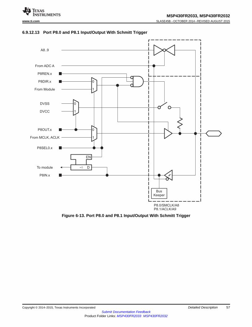
0
1
0
1
P8IN.x
To module
P8SEL0.x
From MCLK, ACLK
P8OUT.x
P8DIR.x 0
1From Module
DVCC
DVSS
P8REN.x
EN
D
BusKeeper
P8.0/SMCLK/A8P8.1/ACLK/A9
From ADC A
A8..9
MSP430FR2033, MSP430FR2032www.ti.com SLASE45B –OCTOBER 2014–REVISED AUGUST 2015
6.9.12.13 Port P8.0 and P8.1 Input/Output With Schmitt Trigger
Figure 6-13. Port P8.0 and P8.1 Input/Output With Schmitt Trigger
Copyright © 2014–2015, Texas Instruments Incorporated Detailed Description 57Submit Documentation Feedback
Product Folder Links: MSP430FR2033 MSP430FR2032

MSP430FR2033, MSP430FR2032SLASE45B –OCTOBER 2014–REVISED AUGUST 2015 www.ti.com
Table 6-26. Port P8.0 and P8.1 Pin Functions
CONTROL BITS AND SIGNALS (1)PIN NAME (P8.x) x FUNCTION
P8DIR.x P8SEL0.x ADCPCTLx (2)
P8.0 (I/O) I: 0; O: 1 0 0VSS 0
P8.0/SMCLK/A8 0 1 0SMCLK 1A8 X X 1 (x = 8)P8.1 (I/O) I: 0; O: 1 0 0VSS 0
P8.1/ACLK/A9 1 1 0ACLK 1A9 X X 1 (x = 9)
(1) X = don't care(2) Setting the ADCPCTLx bit in SYSCFG2 register disables both the output driver and the input Schmitt trigger to prevent leakage when
analog signals are applied.
58 Detailed Description Copyright © 2014–2015, Texas Instruments IncorporatedSubmit Documentation Feedback
Product Folder Links: MSP430FR2033 MSP430FR2032

0
1
0
1
P8IN.x
To module
P8SEL0.x
From Module
P8OUT.x
P8DIR.x 0
1From Module
DVCC
DVSS
P8REN.x
EN
D
BusKeeper
P8.2/TA1CLKP8.3/TA1.2
MSP430FR2033, MSP430FR2032www.ti.com SLASE45B –OCTOBER 2014–REVISED AUGUST 2015
6.9.12.14 Port P8.2 and P8.3 Input/Output With Schmitt Trigger
Figure 6-14. Port P8.2 and P8.3 Input/Output With Schmitt Trigger
Table 6-27. Port P8.2 and P8.3 Pin Functions
CONTROL BITS AND SIGNALSPIN NAME (P8.x) x FUNCTION
P8DIR.x P8SEL0.xP8.2 (I/O) I: 0; O: 1 0
P8.2/TA1CLK 2 TA1 CLK 01
VSS 1P8.3 (I/O) I: 0; O: 1 0
P8.3/TA1.2 3 TA1.CCI2A 01
TA1.2 1
Copyright © 2014–2015, Texas Instruments Incorporated Detailed Description 59Submit Documentation Feedback
Product Folder Links: MSP430FR2033 MSP430FR2032

MSP430FR2033, MSP430FR2032SLASE45B –OCTOBER 2014–REVISED AUGUST 2015 www.ti.com
6.10 Device Descriptors (TLV)Table 6-28 lists the Device IDs of the MSP430FR203x device variants. Table 6-29 lists the contents of thedevice descriptor tag-length-value (TLV) structure for MSP430FR203x devices.
Table 6-28. Device IDs
DEVICE IDDEVICE
1A04h 1A05hMSP430FR2033 75h 82hMSP430FR2032 78h 82h
Table 6-29. Device Descriptors
MSP430FR203xDESCRIPTION
ADDRESS VALUEInfo length 1A00h 06hCRC length 1A01h 06h
1A02h per unitCRC value (1)
1A03h per unitInformation Block
1A04hDevice ID See Table 6-28
1A05hHardware revision 1A06h per unitFirmware revision 1A07h per unitDie Record Tag 1A08h 08hDie Record length 1A09h 0Ah
1A0Ah per unit1A0Bh per unit
Lot Wafer ID1A0Ch per unit1A0Dh per unit
Die Record1A0Eh per unit
Die X position1A0Fh per unit1A10h per unit
Die Y position1A11h per unit1A12h per unit
Test Result1A13h per unit
ADC Calibration Tag 1A14h 11hADC Calibration Length 1A15h 08h
1A16h per unitADC Gain Factor
1A17h per unit1A18h per unit
ADC Calibration ADC Offset1A19h per unit1A1Ah per unit
ADC 1.5-V Reference Temperature 30°C1A1Bh per unit1A1Ch per unit
ADC 1.5-V Reference Temperature 85°C1A1Dh per unit
(1) The CRC value covers the checksum from 1A04h to 1A77h by applying the CRC-CCITT-16 polynomial of x16 + x12 + x5 + 1.
60 Detailed Description Copyright © 2014–2015, Texas Instruments IncorporatedSubmit Documentation Feedback
Product Folder Links: MSP430FR2033 MSP430FR2032

MSP430FR2033, MSP430FR2032www.ti.com SLASE45B –OCTOBER 2014–REVISED AUGUST 2015
Table 6-29. Device Descriptors (continued)MSP430FR203x
DESCRIPTIONADDRESS VALUE
Calibration Tag 1A1Eh 12hCalibration Length 1A1Fh 04h
1A20h per unitReference and DCO Calibration 1.5-V Reference Factor
1A21h per unit1A22h per unitDCO Tap Settings for 16 MHz, Temperature
30°C (2) 1A23h perunit
(2) This value can be directly loaded into DCO bits in CSCTL0 register to get accurate 16-MHz frequency at room temperature, especiallywhen MCU exits from LPM3 and below. TI suggests using a predivider to decrease the frequency, if the temperature drift might result anovershoot beyond 16 MHz.
6.11 MemoryTable 6-30 shows the memory organization of the MSP430FR203x devices.
Table 6-30. Memory Organization
Access MSP430FR2033 MSP430FR2032Memory (FRAM) 15KB 8KBRead/WriteMain: interrupt vectors and signatures FFFFh-FF80h FFFFh-FF80h(Optional Write Protect) (1)Main: code memory FFFFh-C400h FFFFh-E000h
2KB 1KBRAM Read/Write 27FFh-2000h 23FFh-2000hRead/Write 512B 512BInformation Memory (FRAM) (Optional Write Protect) (2) 19FFh-1800h 19FFh-1800h
1KB 1KBBootstrap loader (BSL) Memory (ROM) Read only 13FFh-1000h 13FFh-1000h4KB 4KBPeripherals Read/Write 0FFFh-0000h 0FFFh-0000h
(1) The Program FRAM can be write protected by setting PFWP bit in SYSCFG0 register. Refer to the SYS chapter in the MSP430FR4xxand MSP430FR2xx Family User's Guide (SLAU445) for more details
(2) The Information FRAM can be write protected by setting DFWP bit in SYSCFG0 register. Refer to the SYS chapter in theMSP430FR4xx and MSP430FR2xx Family User's Guide (SLAU445) for more details
Copyright © 2014–2015, Texas Instruments Incorporated Detailed Description 61Submit Documentation Feedback
Product Folder Links: MSP430FR2033 MSP430FR2032

MSP430FR2033, MSP430FR2032SLASE45B –OCTOBER 2014–REVISED AUGUST 2015 www.ti.com
6.11.1 Peripheral File MapTable 6-31 shows the base address and the memory size of the register region for each peripheral, andTable 6-32 through Table 6-50 show all of the available registers for each peripheral and their addressoffsets.
Table 6-31. Peripherals Summary
MODULE NAME BASE ADDRESS SIZESpecial Functions (See Table 6-32) 0100h 0010hPMM (See Table 6-33) 0120h 0020hSYS (See Table 6-34) 0140h 0030hCS (See Table 6-35) 0180h 0020hFRAM (See Table 6-36) 01A0h 0010hCRC (See Table 6-37) 01C0h 0008hWDT (See Table 6-38) 01CCh 0002hPort P1, P2 (See Table 6-39) 0200h 0020hPort P3, P4 (See Table 6-40) 0220h 0020hPort P5, P6 (See Table 6-41) 0240h 0020hPort P7, P8 (See Table 6-42) 0260h 0020hCapacitive Touch I/O (See Table 6-43) 02E0h 0010hTimer0_A3 (See Table 6-44) 0300h 0030hTimer1_A3 (See Table 6-45) 0340h 0030hRTC (See Table 6-46) 03C0h 0010heUSCI_A0 (See Table 6-47) 0500h 0020heUSCI_B0 (See Table 6-48) 0540h 0030hBackup Memory (See Table 6-49) 0660h 0020hADC (See Table 6-50) 0700h 0040h
62 Detailed Description Copyright © 2014–2015, Texas Instruments IncorporatedSubmit Documentation Feedback
Product Folder Links: MSP430FR2033 MSP430FR2032

MSP430FR2033, MSP430FR2032www.ti.com SLASE45B –OCTOBER 2014–REVISED AUGUST 2015
Table 6-32. Special Function Registers (Base Address: 0100h)
REGISTER DESCRIPTION REGISTER OFFSETSFR interrupt enable SFRIE1 00hSFR interrupt flag SFRIFG1 02hSFR reset pin control SFRRPCR 04h
Table 6-33. PMM Registers (Base Address: 0120h)
REGISTER DESCRIPTION REGISTER OFFSETPMM Control 0 PMMCTL0 00hPMM Control 1 PMMCTL1 02hPMM Control 2 PMMCTL2 04hPMM interrupt flags PMMIFG 0AhPM5 Control 0 PM5CTL0 10h
Table 6-34. SYS Registers (Base Address: 0140h)
REGISTER DESCRIPTION REGISTER OFFSETSystem control SYSCTL 00hBootstrap loader configuration area SYSBSLC 02hJTAG mailbox control SYSJMBC 06hJTAG mailbox input 0 SYSJMBI0 08hJTAG mailbox input 1 SYSJMBI1 0AhJTAG mailbox output 0 SYSJMBO0 0ChJTAG mailbox output 1 SYSJMBO1 0EhBus Error vector generator SYSBERRIV 18hUser NMI vector generator SYSUNIV 1AhSystem NMI vector generator SYSSNIV 1ChReset vector generator SYSRSTIV 1EhSystem configuration 0 SYSCFG0 20hSystem configuration 1 SYSCFG1 22hSystem configuration 2 SYSCFG2 24h
Table 6-35. CS Registers (Base Address: 0180h)
REGISTER DESCRIPTION REGISTER OFFSETCS control register 0 CSCTL0 00hCS control register 1 CSCTL1 02hCS control register 2 CSCTL2 04hCS control register 3 CSCTL3 06hCS control register 4 CSCTL4 08hCS control register 5 CSCTL5 0AhCS control register 6 CSCTL6 0ChCS control register 7 CSCTL7 0EhCS control register 8 CSCTL8 10h
Table 6-36. FRAM Registers (Base Address: 01A0h)
REGISTER DESCRIPTION REGISTER OFFSETFRAM control 0 FRCTL0 00hGeneral control 0 GCCTL0 04hGeneral control 1 GCCTL1 06h
Copyright © 2014–2015, Texas Instruments Incorporated Detailed Description 63Submit Documentation Feedback
Product Folder Links: MSP430FR2033 MSP430FR2032

MSP430FR2033, MSP430FR2032SLASE45B –OCTOBER 2014–REVISED AUGUST 2015 www.ti.com
Table 6-37. CRC Registers (Base Address: 01C0h)
REGISTER DESCRIPTION REGISTER OFFSETCRC data input CRC16DI 00hCRC data input reverse byte CRCDIRB 02hCRC initialization and result CRCINIRES 04hCRC result reverse byte CRCRESR 06h
Table 6-38. WDT Registers (Base Address: 01CCh)
REGISTER DESCRIPTION REGISTER OFFSETWatchdog timer control WDTCTL 00h
Table 6-39. Port P1, P2 Registers (Base Address: 0200h)
REGISTER DESCRIPTION REGISTER OFFSETPort P1 input P1IN 00hPort P1 output P1OUT 02hPort P1 direction P1DIR 04hPort P1 pulling register enable P1REN 06hPort P1 selection 0 P1SEL0 0AhPort P1 interrupt vector word P1IV 0EhPort P1 interrupt edge select P1IES 18hPort P1 interrupt enable P1IE 1AhPort P1 interrupt flag P1IFG 1ChPort P2 input P2IN 01hPort P2 output P2OUT 03hPort P2 direction P2DIR 05hPort P2 pulling register enable P2REN 07hPort P2 selection 0 (1) P2SEL0 0BhPort P2 interrupt vector word P2IV 1EhPort P2 interrupt edge select P2IES 19hPort P2 interrupt enable P2IE 1BhPort P2 interrupt flag P2IFG 1Dh
(1) Port P2 selection register does not feature any valid bits. P2SEL0 presents for 16-bit Port A operation with P1SEL0.
Table 6-40. Port P3, P4 Registers (Base Address: 0220h)
REGISTER DESCRIPTION REGISTER OFFSETPort P3 input P3IN 00hPort P3 output P3OUT 02hPort P3 direction P3DIR 04hPort P3 pulling register enable P3REN 06hPort P3 selection 0 (1) P3SEL0 0AhPort P4 input P4IN 01hPort P4 output P4OUT 03hPort P4 direction P4DIR 05hPort P4 pulling register enable P4REN 07hPort P4 selection 0 P4SEL0 0Bh
(1) Port P3 selection register does not feature any valid bits. P3SEL0 presents for 16-bit Port B operation with P4SEL0.
64 Detailed Description Copyright © 2014–2015, Texas Instruments IncorporatedSubmit Documentation Feedback
Product Folder Links: MSP430FR2033 MSP430FR2032

MSP430FR2033, MSP430FR2032www.ti.com SLASE45B –OCTOBER 2014–REVISED AUGUST 2015
Table 6-41. Port P5, P6 Registers (Base Address: 0240h)
REGISTER DESCRIPTION REGISTER OFFSETPort P5 input P5IN 00hPort P5 output P5OUT 02hPort P5 direction P5DIR 04hPort P5 pulling register enable P5REN 06hPort P5 selection 0 P5SEL0 0AhPort P6 input P6IN 01hPort P6 output P6OUT 03hPort P6 direction P6DIR 05hPort P6 pulling register enable P6REN 07hPort P6 selection 0 (1) P6SEL0 0Bh
(1) Port P6 selection register does not feature any valid bits. P6SEL0 presents for 16-bit Port C operation with P5SEL0.
Table 6-42. Port P7, P8 Registers (Base Address: 0260h)
REGISTER DESCRIPTION REGISTER OFFSETPort P7 input P7IN 00hPort P7 output P7OUT 02hPort P7 direction P7DIR 04hPort P7 pulling register enable P7REN 06hPort P7 selection 0 (1) P7SEL0 0AhPort P8 input P8IN 01hPort P8 output P8OUT 03hPort P8 direction P8DIR 05hPort P8 pulling register enable P8REN 07hPort P8 selection 0 P8SEL0 0Bh
(1) Port P7 selection register does not feature any valid bits. P7SEL0 presents for 16-bit Port D operation with P8SEL0.
Table 6-43. Capacitive Touch I/O Registers (Base Address: 02E0h)
REGISTER DESCRIPTION REGISTER OFFSETCapacitive Touch I/O 0 control CAPTIO0CTL 0Eh
Table 6-44. Timer0_A3 Registers (Base Address: 0300h)
REGISTER DESCRIPTION REGISTER OFFSETTA0 control TA0CTL 00hCapture/compare control 0 TA0CCTL0 02hCapture/compare control 1 TA0CCTL1 04hCapture/compare control 2 TA0CCTL2 06hTA0 counter register TA0R 10hCapture/compare register 0 TA0CCR0 12hCapture/compare register 1 TA0CCR1 14hCapture/compare register 2 TA0CCR2 16hTA0 expansion register 0 TA0EX0 20hTA0 interrupt vector TA0IV 2Eh
Copyright © 2014–2015, Texas Instruments Incorporated Detailed Description 65Submit Documentation Feedback
Product Folder Links: MSP430FR2033 MSP430FR2032

MSP430FR2033, MSP430FR2032SLASE45B –OCTOBER 2014–REVISED AUGUST 2015 www.ti.com
Table 6-45. Timer1_A3 Registers (Base Address: 0340h)
REGISTER DESCRIPTION REGISTER OFFSETTA1 control TA1CTL 00hCapture/compare control 0 TA1CCTL0 02hCapture/compare control 1 TA1CCTL1 04hCapture/compare control 2 TA1CCTL2 06hTA1 counter register TA1R 10hCapture/compare register 0 TA1CCR0 12hCapture/compare register 1 TA1CCR1 14hCapture/compare register 2 TA1CCR2 16hTA1 expansion register 0 TA1EX0 20hTA1 interrupt vector TA1IV 2Eh
Table 6-46. RTC Registers (Base Address: 03C0h)
REGISTER DESCRIPTION REGISTER OFFSETRTC control RTCCTL 00hRTC interrupt vector RTCIV 04hRTC modulo RTCMOD 08hRTC counter RTCCNT 0Ch
Table 6-47. eUSCI_A0 Registers (Base Address: 0500h)
REGISTER DESCRIPTION REGISTER OFFSETeUSCI_A control word 0 UCA0CTLW0 00heUSCI_A control word 1 UCA0CTLW1 02heUSCI_A control rate 0 UCA0BR0 06heUSCI_A control rate 1 UCA0BR1 07heUSCI_A modulation control UCA0MCTLW 08heUSCI_A status UCA0STAT 0AheUSCI_A receive buffer UCA0RXBUF 0CheUSCI_A transmit buffer UCA0TXBUF 0EheUSCI_A LIN control UCA0ABCTL 10heUSCI_A IrDA transmit control lUCA0IRTCTL 12heUSCI_A IrDA receive control IUCA0IRRCTL 13heUSCI_A interrupt enable UCA0IE 1AheUSCI_A interrupt flags UCA0IFG 1CheUSCI_A interrupt vector word UCA0IV 1Eh
Table 6-48. eUSCI_B0 Registers (Base Address: 0540h)
REGISTER DESCRIPTION REGISTER OFFSETeUSCI_B control word 0 UCB0CTLW0 00heUSCI_B control word 1 UCB0CTLW1 02heUSCI_B bit rate 0 UCB0BR0 06heUSCI_B bit rate 1 UCB0BR1 07heUSCI_B status word UCB0STATW 08heUSCI_B byte counter threshold UCB0TBCNT 0AheUSCI_B receive buffer UCB0RXBUF 0CheUSCI_B transmit buffer UCB0TXBUF 0EheUSCI_B I2C own address 0 UCB0I2COA0 14h
66 Detailed Description Copyright © 2014–2015, Texas Instruments IncorporatedSubmit Documentation Feedback
Product Folder Links: MSP430FR2033 MSP430FR2032

MSP430FR2033, MSP430FR2032www.ti.com SLASE45B –OCTOBER 2014–REVISED AUGUST 2015
Table 6-48. eUSCI_B0 Registers (Base Address: 0540h) (continued)REGISTER DESCRIPTION REGISTER OFFSET
eUSCI_B I2C own address 1 UCB0I2COA1 16heUSCI_B I2C own address 2 UCB0I2COA2 18heUSCI_B I2C own address 3 UCB0I2COA3 1AheUSCI_B receive address UCB0ADDRX 1CheUSCI_B address mask UCB0ADDMASK 1EheUSCI_B I2C slave address UCB0I2CSA 20heUSCI_B interrupt enable UCB0IE 2AheUSCI_B interrupt flags UCB0IFG 2CheUSCI_B interrupt vector word UCB0IV 2Eh
Table 6-49. Backup Memory Registers (Base Address: 0660h)
REGISTER DESCRIPTION REGISTER OFFSETBackup Memory 0 BAKMEM0 00hBackup Memory 1 BAKMEM1 02hBackup Memory 2 BAKMEM2 04hBackup Memory 3 BAKMEM3 06hBackup Memory 4 BAKMEM4 08hBackup Memory 5 BAKMEM5 0AhBackup Memory 6 BAKMEM6 0ChBackup Memory 7 BAKMEM7 0EhBackup Memory 8 BAKMEM8 10hBackup Memory 9 BAKMEM9 12hBackup Memory 10 BAKMEM10 14hBackup Memory 11 BAKMEM11 16hBackup Memory 12 BAKMEM12 18hBackup Memory 13 BAKMEM13 1AhBackup Memory 14 BAKMEM14 1ChBackup Memory 15 BAKMEM15 1Eh
Table 6-50. ADC Registers (Base Address: 0700h)
REGISTER DESCRIPTION REGISTER OFFSETADC control register 0 ADCCTL0 00hADC control register 1 ADCCTL1 02hADC control register 2 ADCCTL2 04hADC window comparator low threshold ADCLO 06hADC window comparator high threshold ADCHI 08hADC memory control register 0 ADCMCTL0 0AhADC conversion memory register ADCMEM0 12hADC interrupt enable ADCIE 1AhADC interrupt flags ADCIFG 1ChADC interrupt vector word ADCIV 1Eh
Copyright © 2014–2015, Texas Instruments Incorporated Detailed Description 67Submit Documentation Feedback
Product Folder Links: MSP430FR2033 MSP430FR2032

MSP430FR2033, MSP430FR2032SLASE45B –OCTOBER 2014–REVISED AUGUST 2015 www.ti.com
6.12 Identification
6.12.1 Revision IdentificationThe device revision information is shown as part of the top-side marking on the device package. Thedevice-specific errata sheet describes these markings. For links to the errata sheets for the devices in thisdata sheet, see Section 8.2.
The hardware revision is also stored in the Device Descriptor structure in the Info Block section. Fordetails on this value, see the "Hardware Revision" entries in Section 6.10.
6.12.2 Device IdentificationThe device type can be identified from the top-side marking on the device package. The device-specificerrata sheet describes these markings. For links to the errata sheets for the devices in this data sheet, seeSection 8.2.
A device identification value is also stored in the Device Descriptor structure in the Info Block section. Fordetails on this value, see the "Device ID" entries in Section 6.10.
6.12.3 JTAG IdentificationProgramming through the JTAG interface, including reading and identifying the JTAG ID, is described indetail in the MSP430 Programming Via the JTAG Interface User's Guide (SLAU320).
68 Detailed Description Copyright © 2014–2015, Texas Instruments IncorporatedSubmit Documentation Feedback
Product Folder Links: MSP430FR2033 MSP430FR2032

CL1
CL2
XIN XOUT
Power SupplyDecoupling
100 nF10 Fµ
DVCC
DVSS
+
MSP430FR2033, MSP430FR2032www.ti.com SLASE45B –OCTOBER 2014–REVISED AUGUST 2015
7 Applications, Implementation, and Layout
NOTEInformation in the following applications sections is not part of the TI componentspecification, and TI does not warrant its accuracy or completeness. TI’s customers areresponsible for determining suitability of components for their purposes. Customers shouldvalidate and test their design implementation to confirm system functionality.
7.1 Device Connection and Layout FundamentalsThis section discusses the recommended guidelines when designing with the MSP430FR413x devices.These guidelines are to make sure that the device has proper connections for powering, programming,debugging, and optimum analog performance.
7.1.1 Power Supply Decoupling and Bulk CapacitorsTI recommends connecting a combination of a 10-µF plus a 100-nF low-ESR ceramic decouplingcapacitor to the DVCC and DVSS pins. Higher-value capacitors may be used but can impact supply railramp-up time. Decoupling capacitors must be placed as close as possible to the pins that they decouple(within a few millimeters).
Figure 7-1. Power Supply Decoupling
7.1.2 External OscillatorThis device supports only a low-frequency crystal (32 kHz) on the XIN and XOUT pins. External bypasscapacitors for the crystal oscillator pins are required.
It is also possible to apply digital clock signals to the XIN input pin that meet the specifications of therespective oscillator if the appropriate XT1BYPASS mode is selected. In this case, the associated XOUTpin can be used for other purposes. If they are left unused, they must be terminated according toSection 4.4.
Figure 7-2 shows a typical connection diagram.
Figure 7-2. Typical Crystal Connection
See the application report MSP430 32-kHz Crystal Oscillators (SLAA322) for more information onselecting, testing, and designing a crystal oscillator with the MSP430 devices.
Copyright © 2014–2015, Texas Instruments Incorporated Applications, Implementation, and Layout 69Submit Documentation Feedback
Product Folder Links: MSP430FR2033 MSP430FR2032

1
3
5
7
9
11
13
2
4
6
8
10
12
14
TDO/TDI
TDI
TMS
TCK
GND
TEST
JTAG
VCC TOOL
VCC TARGET
J1 (see Note A)
J2 (see Note A)
VCC
R1
47 kW
DVCC
RST/NMI/SBWTDIO
TDO/TDI
TDI
TMS
TCK
TEST/SBWTCK
DVSS
MSP430FRxxx
C11 nF
(see Note B)
RST
Important to connect
MSP430FR2033, MSP430FR2032SLASE45B –OCTOBER 2014–REVISED AUGUST 2015 www.ti.com
7.1.3 JTAGWith the proper connections, the debugger and a hardware JTAG interface (such as the MSP-FET orMSP-FET430UIF) can be used to program and debug code on the target board. In addition, theconnections also support the MSP-GANG production programmers, thus providing an easy way toprogram prototype boards, if desired. Figure 7-3 shows the connections between the 14-pin JTAGconnector and the target device required to support in-system programming and debugging for 4-wireJTAG communication. Figure 7-4 shows the connections for 2-wire JTAG mode (Spy-Bi-Wire).
The connections for the MSP-FET and MSP-FET430UIF interface modules and the MSP-GANG areidentical. Both can supply VCC to the target board (through pin 2). In addition, the MSP-FET and MSP-FET430UIF interface modules and MSP-GANG have a VCC sense feature that, if used, requires analternate connection (pin 4 instead of pin 2). The VCC-sense feature senses the local VCC present on thetarget board (that is, a battery or other local power supply) and adjusts the output signals accordingly.Figure 7-3 and Figure 7-4 show a jumper block that supports both scenarios of supplying VCC to thetarget board. If this flexibility is not required, the desired VCC connections may be hard-wired to eliminatethe jumper block. Pins 2 and 4 must not be connected at the same time.
For additional design information regarding the JTAG interface, see the MSP430 Hardware Tools User’sGuide (SLAU278).
A. If a local target power supply is used, make connection J1. If power from the debug or programming adapter is used,make connection J2.
B. The upper limit for C1 is 1.1 nF when using current TI tools.
Figure 7-3. Signal Connections for 4-Wire JTAG Communication
70 Applications, Implementation, and Layout Copyright © 2014–2015, Texas Instruments IncorporatedSubmit Documentation Feedback
Product Folder Links: MSP430FR2033 MSP430FR2032

1
3
5
7
9
11
13
2
4
6
8
10
12
14
TEST/SBWTCK
MSP430FRxxx
RST/NMI/SBWTDIOTDO/TDI
TCK
GND
JTAG
R147 kΩ
(see Note B)
VCC TOOL
VCC TARGET
C11 nF
(see Note B)
J1 (see Note A)
J2 (see Note A)
Important to connect
DVCC
DVSS
VCC
MSP430FR2033, MSP430FR2032www.ti.com SLASE45B –OCTOBER 2014–REVISED AUGUST 2015
A. Make connection J1 if a local target power supply is used, or make connection J2 if the target is powered from thedebug or programming adapter.
B. The device RST/NMI/SBWTDIO pin is used in 2-wire mode for bidirectional communication with the device duringJTAG access, and any capacitance that is attached to this signal may affect the ability to establish a connection withthe device. The upper limit for C1 is 1.1 nF when using current TI tools.
Figure 7-4. Signal Connections for 2-Wire JTAG Communication (Spy-Bi-Wire)
7.1.4 ResetThe reset pin can be configured as a reset function (default) or as an NMI function in the Special FunctionRegister (SFR), SFRRPCR.
In reset mode, the RST/NMI pin is active low, and a pulse applied to this pin that meets the reset timingspecifications generates a BOR-type device reset.
Setting SYSNMI causes the RST/NMI pin to be configured as an external NMI source. The external NMI isedge sensitive, and its edge is selectable by SYSNMIIES. Setting the NMIIE enables the interrupt of theexternal NMI. When an external NMI event occurs, the NMIIFG is set.
The RST/NMI pin can have either a pullup or pulldown that is enabled or not. SYSRSTUP selects eitherpullup or pulldown, and SYSRSTRE causes the pullup (default) or pulldown to be enabled (default) or not.If the RST/NMI pin is unused, it is required either to select and enable the internal pullup or to connect anexternal 47-kΩ pullup resistor to the RST/NMI pin with a 1.1-nF pulldown capacitor. The pulldowncapacitor should not exceed 1.1 nF when using devices with Spy-Bi-Wire interface in Spy-Bi-Wire mode orin 4-wire JTAG mode with TI tools like FET interfaces or GANG programmers.
See the device family user’s guide (SLAU367) for more information on the referenced control registersand bits.
7.1.5 Unused PinsFor details on the connection of unused pins, see Section 4.4.
Copyright © 2014–2015, Texas Instruments Incorporated Applications, Implementation, and Layout 71Submit Documentation Feedback
Product Folder Links: MSP430FR2033 MSP430FR2032

Using anExternalPositiveReference
Using anExternalNegativeReference
VEREF-
VREF+/VEREF+
+
+
100 nF10 Fµ
100 nF10 Fµ
DVSS
MSP430FR2033, MSP430FR2032SLASE45B –OCTOBER 2014–REVISED AUGUST 2015 www.ti.com
7.1.6 General Layout Recommendations• Proper grounding and short traces for external crystal to reduce parasitic capacitance. See the
application report MSP430 32-kHz Crystal Oscillators (SLAA322) for recommended layout guidelines.• Proper bypass capacitors on DVCC and reference pins, if used.• Avoid routing any high-frequency signal close to an analog signal line. For example, keep digital
switching signals such as PWM or JTAG signals away from the oscillator circuit.• Refer to the Circuit Board Layout Techniques design guide (SLOA089) for a detailed discussion of
PCB layout considerations. This document is written primarily about op amps, but the guidelines aregenerally applicable for all mixed-signal applications.
• Proper ESD level protection should be considered to protect the device from unintended high-voltageelectrostatic discharge. See the application report MSP430 System-Level ESD Considerations(SLAA530) for guidelines.
7.1.7 Do's and Don'tsDuring power up, power down, and device operation, DVCC must not exceed the limits specified inSection 5.1, Absolute Maximum Ratings. Exceeding the specified limits may cause malfunction of thedevice including erroneous writes to RAM and FRAM.
7.2 Peripheral- and Interface-Specific Design Information
7.2.1 ADC Peripheral
7.2.1.1 Partial Schematic
Figure 7-5. ADC Grounding and Noise Considerations
7.2.1.2 Design Requirements
As with any high-resolution ADC, appropriate printed-circuit-board layout and grounding techniques shouldbe followed to eliminate ground loops, unwanted parasitic effects, and noise.
Ground loops are formed when return current from the ADC flows through paths that are common withother analog or digital circuitry. If care is not taken, this current can generate small unwanted offsetvoltages that can add to or subtract from the reference or input voltages of the ADC. The generalguidelines in Section 7.1.1 combined with the connections shown in Section 7.2.1.1 prevent this.
In addition to grounding, ripple and noise spikes on the power-supply lines that are caused by digitalswitching or switching power supplies can corrupt the conversion result. TI recommends a noise-freedesign using separate analog and digital ground planes with a single-point connection to achieve highaccuracy.
72 Applications, Implementation, and Layout Copyright © 2014–2015, Texas Instruments IncorporatedSubmit Documentation Feedback
Product Folder Links: MSP430FR2033 MSP430FR2032

MSP430FR2033, MSP430FR2032www.ti.com SLASE45B –OCTOBER 2014–REVISED AUGUST 2015
Figure 7-5 shows the recommended decoupling circuit when an external voltage reference is used. Theinternal reference module has a maximum drive current as described in the sections ADC Pin Enable and1.2-V Reference Settings of the MSP430FR4xx and MSP430FR2xx Family User's Guide (SLAU445).
The reference voltage must be a stable voltage for accurate measurements. The capacitor values that areselected in the general guidelines filter out the high- and low-frequency ripple before the reference voltageenters the device. In this case, the 10-μF capacitor is used to buffer the reference pin and filter any low-frequency ripple. A bypass capacitor of 100 nF is used to filter out any high-frequency noise.
7.2.1.3 Layout Guidelines
Components that are shown in the partial schematic (see Figure 7-5) should be placed as close aspossible to the respective device pins to avoid long traces, because they add additional parasiticcapacitance, inductance, and resistance on the signal.
Avoid routing analog input signals close to a high-frequency pin (for example, a high-frequency PWM),because the high-frequency switching can be coupled into the analog signal.
Copyright © 2014–2015, Texas Instruments Incorporated Applications, Implementation, and Layout 73Submit Documentation Feedback
Product Folder Links: MSP430FR2033 MSP430FR2032

MSP430FR2033, MSP430FR2032SLASE45B –OCTOBER 2014–REVISED AUGUST 2015 www.ti.com
8 Device and Documentation Support
8.1 Device Support
8.1.1 Development Support
8.1.1.1 Getting Started and Next Steps
For an introduction to the MSP430 family of devices and the tools and libraries that are available to helpwith your development, visit the Getting Started page.
8.1.1.2 Development Tools Support
8.1.1.2.1 Hardware Features
See the Code Composer Studio for MSP430 User's Guide (SLAU157) for details on the available features.BREAK- RANGE LPMX.5MSP430 4-WIRE 2-WIRE CLOCK STATE TRACEPOINTS BREAK- DEBUGGINGARCHITECTURE JTAG JTAG CONTROL SEQUENCER BUFFER(N) POINTS SUPPORT
MSP430Xv2 Yes Yes 3 Yes Yes No No No
8.1.1.2.2 Recommended Hardware Options
All MSP430™ microcontrollers are supported by a wide variety of software and hardware developmenttools. Tools are available from TI and various third parties. See them all at www.ti.com/msp430tools.
8.1.1.2.2.1 Target Socket Boards
The target socket boards allow easy programming and debugging of the device using JTAG. They alsofeature header pin outs for prototyping. Target socket boards are orderable individually or as a kit with theJTAG programmer and debugger included. The following table shows the compatible target boards andthe supported packages.
PACKAGE TARGET BOARD AND PROGRAMMER BUNDLE TARGET BOARD ONLY64-pin LQFP (PM) MSP-FET430U64D MSP-TS430PM64D
8.1.1.2.2.2 Experimenter Boards
Experimenter Boards and Evaluation kits are available for some MSP430 devices. These kits featureadditional hardware components and connectivity for full system evaluation and prototyping. Seewww.ti.com/msp430tools for details.
8.1.1.2.2.3 Debugging and Programming Tools
Hardware programming and debugging tools are available from TI and from its third party suppliers. Seethe full list of available tools at www.ti.com/msp430tools.
8.1.1.2.2.4 Production Programmers
The production programmers expedite loading firmware to devices by programming several devicessimultaneously.
PART NUMBER PC PORT FEATURES PROVIDERProgram up to eight devices at a time. Works with PC or as aMSP-GANG Serial and USB Texas Instrumentsstand-alone device.
74 Device and Documentation Support Copyright © 2014–2015, Texas Instruments IncorporatedSubmit Documentation Feedback
Product Folder Links: MSP430FR2033 MSP430FR2032

MSP430FR2033, MSP430FR2032www.ti.com SLASE45B –OCTOBER 2014–REVISED AUGUST 2015
8.1.1.2.3 Recommended Software Options
8.1.1.2.3.1 Integrated Development Environments
Software development tools are available from TI or from third parties. Open source solutions are alsoavailable.
This device is supported by Code Composer Studio™ IDE (CCS).
8.1.1.2.3.2 MSP430Ware
MSP430Ware is a collection of code examples, data sheets, and other design resources for all MSP430devices delivered in a convenient package. In addition to providing a complete collection of existingMSP430 design resources, MSP430Ware also includes a high-level API called MSP430 Driver Library.This library makes it easy to program MSP430 hardware. MSP430Ware is available as a component ofCCS or as a stand-alone package.
8.1.1.2.3.3 Command-Line Programmer
MSP430 Flasher is an open-source, shell-based interface for programming MSP430 microcontrollersthrough a FET programmer or eZ430 using JTAG or Spy-Bi-Wire (SBW) communication. MSP430 Flashercan be used to download binary files (.txt or .hex) files directly to the MSP430 microcontroller without theneed for an IDE.
8.1.2 Device and Development Tool NomenclatureTo designate the stages in the product development cycle, TI assigns prefixes to the part numbers of allMSP430 MCU devices and support tools. Each MSP430 MCU commercial family member has one ofthree prefixes: MSP, PMS, or XMS (for example, MSP430FR2033). TI recommends two of three possibleprefix designators for its support tools: MSP and MSPX. These prefixes represent evolutionary stages ofproduct development from engineering prototypes (with XMS for devices and MSPX for tools) through fullyqualified production devices and tools (with MSP for devices and MSP for tools).
Device development evolutionary flow:
XMS – Experimental device that is not necessarily representative of the electrical specifications of the finaldevice
MSP – Fully qualified production device
Support tool development evolutionary flow:
MSPX – Development-support product that has not yet completed TI internal qualification testing.
MSP – Fully qualified development-support product
XMS devices and MSPX development-support tools are shipped against the following disclaimer:
"Developmental product is intended for internal evaluation purposes."
MSP devices and MSP development-support tools have been characterized fully, and the quality andreliability of the device have been demonstrated fully. TI's standard warranty applies.
Predictions show that prototype devices (XMS) have a greater failure rate than the standard productiondevices. TI recommends that these devices not be used in any production system because their expectedend-use failure rate still is undefined. Only qualified production devices are to be used.
TI device nomenclature also includes a suffix with the device family name. This suffix indicates thepackage type (for example, PM) and temperature range (for example, T). Figure 8-1 provides a legend forreading the complete device name for any family member.
Copyright © 2014–2015, Texas Instruments Incorporated Device and Documentation Support 75Submit Documentation Feedback
Product Folder Links: MSP430FR2033 MSP430FR2032

MSP 430 FR 4 133 I PM T
Processor Family
Series Packaging
430 MCU Platform
Optional: Tape and ReelDevice Type
Optional: Temperature RangeFeature Set
Processor Family MSP = Mixed-Signal ProcessorXMS = Experimental Silicon
430 MCU Platform TI’s 16-Bit Low-Power Microcontroller Platform
Device Type
Series
Feature Set
Optional: Temperature Range
Memory TypeFR = FRAM
FRAM 4 Series = Up to 16 MHz with LCDFRAM 2 Series = Up to 16 MHz without LCD
1 and 2 Digit ADC Channels / 16-bit Timers / I/Osst nd
–13 = Up to 10 / 3 / Up to 60
3 Digit FRAM (KB) / SRAM (KB)rd
–3 = 16 / 22 = 8 / 11 = 4 / 0.5
S = 0 C to 50 CC = 0°C to 70°CI –
°°
° °° °
= 40 C to 85 CT = –40 C to 105 C
Packaging http://www.ti.com/packaging
Optional: Distribution Format T = Small reelR = Large reelNo Marking = Tube or Tray
MSP430FR2033, MSP430FR2032SLASE45B –OCTOBER 2014–REVISED AUGUST 2015 www.ti.com
Figure 8-1. Device Nomenclature
8.2 Documentation SupportThe following documents describe the MSP430FR203x microcontrollers. Copies of these documents areavailable on the Internet at www.ti.com.
SLAU445 MSP430FR4xx and MSP430FR2xx Family User's Guide. Detailed description of allmodules and peripherals available in this device family.
SLAZ625 MSP430FR2033 Device Erratasheet. Describes the known exceptions to the functionalspecifications for all silicon revisions of this device.
SLAZ626 MSP430FR2032 Device Erratasheet. Describes the known exceptions to the functionalspecifications for all silicon revisions of this device.
8.2.1 Related LinksTable 8-1 lists quick access links. Categories include technical documents, support and communityresources, tools and software, and quick access to sample or buy.
Table 8-1. Related Links
TECHNICAL TOOLS & SUPPORT &PARTS PRODUCT FOLDER SAMPLE & BUY DOCUMENTS SOFTWARE COMMUNITYMSP430FR2033 Click here Click here Click here Click here Click hereMSP430FR2032 Click here Click here Click here Click here Click here
76 Device and Documentation Support Copyright © 2014–2015, Texas Instruments IncorporatedSubmit Documentation Feedback
Product Folder Links: MSP430FR2033 MSP430FR2032

MSP430FR2033, MSP430FR2032www.ti.com SLASE45B –OCTOBER 2014–REVISED AUGUST 2015
8.2.2 Community ResourcesThe following links connect to TI community resources. Linked contents are provided "AS IS" by therespective contributors. They do not constitute TI specifications and do not necessarily reflect TI's views;see TI's Terms of Use.
TI E2E™ CommunityTI's Engineer-to-Engineer (E2E) Community. Created to foster collaboration among engineers. Ate2e.ti.com, you can ask questions, share knowledge, explore ideas, and help solve problems with fellowengineers.
TI Embedded Processors WikiTexas Instruments Embedded Processors Wiki. Established to help developers get started with embeddedprocessors from Texas Instruments and to foster innovation and growth of general knowledge about thehardware and software surrounding these devices.
8.3 TrademarksMSP430, Code Composer Studio, E2E are trademarks of Texas Instruments.All other trademarks are the property of their respective owners.
8.4 Electrostatic Discharge CautionThis integrated circuit can be damaged by ESD. Texas Instruments recommends that all integrated circuits be handled withappropriate precautions. Failure to observe proper handling and installation procedures can cause damage.
ESD damage can range from subtle performance degradation to complete device failure. Precision integrated circuits may be moresusceptible to damage because very small parametric changes could cause the device not to meet its published specifications.
8.5 GlossarySLYZ022 — TI Glossary.
This glossary lists and explains terms, acronyms, and definitions.
Copyright © 2014–2015, Texas Instruments Incorporated Device and Documentation Support 77Submit Documentation Feedback
Product Folder Links: MSP430FR2033 MSP430FR2032

MSP430FR2033, MSP430FR2032SLASE45B –OCTOBER 2014–REVISED AUGUST 2015 www.ti.com
9 Mechanical Packaging and Orderable Information
9.1 Packaging InformationThe following pages include mechanical packaging and orderable information. This information is the mostcurrent data available for the designated devices. This data is subject to change without notice andrevision of this document. For browser-based versions of this data sheet, refer to the left-hand navigation.
78 Mechanical Packaging and Orderable Information Copyright © 2014–2015, Texas Instruments IncorporatedSubmit Documentation Feedback
Product Folder Links: MSP430FR2033 MSP430FR2032

PACKAGE OPTION ADDENDUM
www.ti.com 31-Jan-2017
Addendum-Page 1
PACKAGING INFORMATION
Orderable Device Status(1)
Package Type PackageDrawing
Pins PackageQty
Eco Plan(2)
Lead/Ball Finish(6)
MSL Peak Temp(3)
Op Temp (°C) Device Marking(4/5)
Samples
MSP430FR2032IG48 ACTIVE TSSOP DGG 48 40 Green (RoHS& no Sb/Br)
CU NIPDAU Level-3-260C-168 HR -40 to 85 FR2032
MSP430FR2032IG48R ACTIVE TSSOP DGG 48 2000 Green (RoHS& no Sb/Br)
CU NIPDAU Level-3-260C-168 HR -40 to 85 FR2032
MSP430FR2032IG56 ACTIVE TSSOP DGG 56 35 Green (RoHS& no Sb/Br)
CU NIPDAU Level-3-260C-168 HR -40 to 85 FR2032
MSP430FR2032IG56R ACTIVE TSSOP DGG 56 2000 Green (RoHS& no Sb/Br)
CU NIPDAU Level-3-260C-168 HR -40 to 85 FR2032
MSP430FR2032IPMR ACTIVE LQFP PM 64 1000 Green (RoHS& no Sb/Br)
CU NIPDAU Level-3-260C-168 HR -40 to 85 FR2032
MSP430FR2033IG48 ACTIVE TSSOP DGG 48 40 Green (RoHS& no Sb/Br)
CU NIPDAU Level-3-260C-168 HR -40 to 85 FR2033
MSP430FR2033IG48R ACTIVE TSSOP DGG 48 2000 Green (RoHS& no Sb/Br)
CU NIPDAU Level-3-260C-168 HR -40 to 85 FR2033
MSP430FR2033IG56 ACTIVE TSSOP DGG 56 35 Green (RoHS& no Sb/Br)
CU NIPDAU Level-3-260C-168 HR -40 to 85 FR2033
MSP430FR2033IG56R ACTIVE TSSOP DGG 56 2000 Green (RoHS& no Sb/Br)
CU NIPDAU Level-3-260C-168 HR -40 to 85 FR2033
MSP430FR2033IPM ACTIVE LQFP PM 64 160 Green (RoHS& no Sb/Br)
CU NIPDAU Level-3-260C-168 HR -40 to 85 FR2033
MSP430FR2033IPMR ACTIVE LQFP PM 64 1000 Green (RoHS& no Sb/Br)
CU NIPDAU Level-3-260C-168 HR -40 to 85 FR2033
(1) The marketing status values are defined as follows:ACTIVE: Product device recommended for new designs.LIFEBUY: TI has announced that the device will be discontinued, and a lifetime-buy period is in effect.NRND: Not recommended for new designs. Device is in production to support existing customers, but TI does not recommend using this part in a new design.PREVIEW: Device has been announced but is not in production. Samples may or may not be available.OBSOLETE: TI has discontinued the production of the device.
(2) Eco Plan - The planned eco-friendly classification: Pb-Free (RoHS), Pb-Free (RoHS Exempt), or Green (RoHS & no Sb/Br) - please check http://www.ti.com/productcontent for the latest availabilityinformation and additional product content details.TBD: The Pb-Free/Green conversion plan has not been defined.Pb-Free (RoHS): TI's terms "Lead-Free" or "Pb-Free" mean semiconductor products that are compatible with the current RoHS requirements for all 6 substances, including the requirement thatlead not exceed 0.1% by weight in homogeneous materials. Where designed to be soldered at high temperatures, TI Pb-Free products are suitable for use in specified lead-free processes.

PACKAGE OPTION ADDENDUM
www.ti.com 31-Jan-2017
Addendum-Page 2
Pb-Free (RoHS Exempt): This component has a RoHS exemption for either 1) lead-based flip-chip solder bumps used between the die and package, or 2) lead-based die adhesive used betweenthe die and leadframe. The component is otherwise considered Pb-Free (RoHS compatible) as defined above.Green (RoHS & no Sb/Br): TI defines "Green" to mean Pb-Free (RoHS compatible), and free of Bromine (Br) and Antimony (Sb) based flame retardants (Br or Sb do not exceed 0.1% by weightin homogeneous material)
(3) MSL, Peak Temp. - The Moisture Sensitivity Level rating according to the JEDEC industry standard classifications, and peak solder temperature.
(4) There may be additional marking, which relates to the logo, the lot trace code information, or the environmental category on the device.
(5) Multiple Device Markings will be inside parentheses. Only one Device Marking contained in parentheses and separated by a "~" will appear on a device. If a line is indented then it is a continuationof the previous line and the two combined represent the entire Device Marking for that device.
(6) Lead/Ball Finish - Orderable Devices may have multiple material finish options. Finish options are separated by a vertical ruled line. Lead/Ball Finish values may wrap to two lines if the finishvalue exceeds the maximum column width.
Important Information and Disclaimer:The information provided on this page represents TI's knowledge and belief as of the date that it is provided. TI bases its knowledge and belief on informationprovided by third parties, and makes no representation or warranty as to the accuracy of such information. Efforts are underway to better integrate information from third parties. TI has taken andcontinues to take reasonable steps to provide representative and accurate information but may not have conducted destructive testing or chemical analysis on incoming materials and chemicals.TI and TI suppliers consider certain information to be proprietary, and thus CAS numbers and other limited information may not be available for release.
In no event shall TI's liability arising out of such information exceed the total purchase price of the TI part(s) at issue in this document sold by TI to Customer on an annual basis.

TAPE AND REEL INFORMATION
*All dimensions are nominal
Device PackageType
PackageDrawing
Pins SPQ ReelDiameter
(mm)
ReelWidth
W1 (mm)
A0(mm)
B0(mm)
K0(mm)
P1(mm)
W(mm)
Pin1Quadrant
MSP430FR2032IG48R TSSOP DGG 48 2000 330.0 24.4 8.6 13.0 1.8 12.0 24.0 Q1
MSP430FR2032IG56R TSSOP DGG 56 2000 330.0 24.4 8.6 15.6 1.8 12.0 24.0 Q1
MSP430FR2032IPMR LQFP PM 64 1000 330.0 24.4 13.0 13.0 2.1 16.0 24.0 Q2
MSP430FR2033IG48R TSSOP DGG 48 2000 330.0 24.4 8.6 13.0 1.8 12.0 24.0 Q1
MSP430FR2033IG56R TSSOP DGG 56 2000 330.0 24.4 8.6 15.6 1.8 12.0 24.0 Q1
MSP430FR2033IPMR LQFP PM 64 1000 330.0 24.4 13.0 13.0 2.1 16.0 24.0 Q2
PACKAGE MATERIALS INFORMATION
www.ti.com 16-Dec-2017
Pack Materials-Page 1

*All dimensions are nominal
Device Package Type Package Drawing Pins SPQ Length (mm) Width (mm) Height (mm)
MSP430FR2032IG48R TSSOP DGG 48 2000 367.0 367.0 45.0
MSP430FR2032IG56R TSSOP DGG 56 2000 367.0 367.0 45.0
MSP430FR2032IPMR LQFP PM 64 1000 367.0 367.0 45.0
MSP430FR2033IG48R TSSOP DGG 48 2000 367.0 367.0 45.0
MSP430FR2033IG56R TSSOP DGG 56 2000 367.0 367.0 45.0
MSP430FR2033IPMR LQFP PM 64 1000 367.0 367.0 45.0
PACKAGE MATERIALS INFORMATION
www.ti.com 16-Dec-2017
Pack Materials-Page 2

www.ti.com
PACKAGE OUTLINE
C
TYP8.37.9
1.2 MAX
54X 0.5
56X 0.270.17
2X13.5
(0.15) TYP
0 - 80.150.05
0.25GAGE PLANE
0.750.50
A
NOTE 3
14.113.9
B 6.26.0
4222167/A 07/2015
TSSOP - 1.2 mm max heightDGG0056ASMALL OUTLINE PACKAGE
NOTES: 1. All linear dimensions are in millimeters. Any dimensions in parenthesis are for reference only. Dimensioning and tolerancing per ASME Y14.5M. 2. This drawing is subject to change without notice. 3. This dimension does not include mold flash, protrusions, or gate burrs. Mold flash, protrusions, or gate burrs shall not exceed 0.15 mm per side.4. Reference JEDEC registration MO-153.
156
0.08 C A B
2928
PIN 1 IDAREA
SEATING PLANE
0.1 C
SEE DETAIL A
DETAIL ATYPICAL
SCALE 1.200

www.ti.com
EXAMPLE BOARD LAYOUT
(7.5)
0.05 MAXALL AROUND
0.05 MINALL AROUND
56X (1.5)
56X (0.3)
54X (0.5)
(R )TYP
0.05
4222167/A 07/2015
TSSOP - 1.2 mm max heightDGG0056ASMALL OUTLINE PACKAGE
SYMM
SYMM
LAND PATTERN EXAMPLESCALE:6X
1
28 29
56
NOTES: (continued) 5. Publication IPC-7351 may have alternate designs. 6. Solder mask tolerances between and around signal pads can vary based on board fabrication site.
METALSOLDER MASKOPENING
NON SOLDER MASKDEFINED
SOLDER MASK DETAILS
SOLDER MASKOPENING
METAL UNDERSOLDER MASK
SOLDER MASKDEFINED

www.ti.com
EXAMPLE STENCIL DESIGN
(7.5)
54X (0.5)
56X (0.3)
56X (1.5)
(R ) TYP0.05
4222167/A 07/2015
TSSOP - 1.2 mm max heightDGG0056ASMALL OUTLINE PACKAGE
NOTES: (continued) 7. Laser cutting apertures with trapezoidal walls and rounded corners may offer better paste release. IPC-7525 may have alternate design recommendations. 8. Board assembly site may have different recommendations for stencil design.
SYMM
SYMM
1
28 29
56
SOLDER PASTE EXAMPLEBASED ON 0.125 mm THICK STENCIL
SCALE:6X

MECHANICAL DATA
MTQF008A – JANUARY 1995 – REVISED DECEMBER 1996
1POST OFFICE BOX 655303 • DALLAS, TEXAS 75265
PM (S-PQFP-G64) PLASTIC QUAD FLATPACK
4040152/C 11/96
32
170,13 NOM
0,25
0,450,75
Seating Plane
0,05 MIN
Gage Plane
0,27
33
16
48
1
0,17
49
64
SQ
SQ10,20
11,8012,20
9,80
7,50 TYP
1,60 MAX
1,451,35
0,08
0,50 M0,08
0°–7°
NOTES: A. All linear dimensions are in millimeters.B. This drawing is subject to change without notice.C. Falls within JEDEC MS-026D. May also be thermally enhanced plastic with leads connected to the die pads.


MECHANICAL DATA
MTSS003D – JANUARY 1995 – REVISED JANUARY 1998
POST OFFICE BOX 655303 • DALLAS, TEXAS 75265
DGG (R-PDSO-G**) PLASTIC SMALL-OUTLINE PACKAGE
4040078/F 12/97
48 PINS SHOWN
0,25
0,15 NOM
Gage Plane
6,006,20 8,30
7,90
0,750,50
Seating Plane
25
0,270,17
24
A
48
1
1,20 MAX
M0,08
0,10
0,50
0°–8°
56
14,10
13,90
48DIM
A MAX
A MIN
PINS **
12,40
12,60
64
17,10
16,90
0,150,05
NOTES: A. All linear dimensions are in millimeters.B. This drawing is subject to change without notice.C. Body dimensions do not include mold protrusion not to exceed 0,15.D. Falls within JEDEC MO-153

IMPORTANT NOTICE
Texas Instruments Incorporated (TI) reserves the right to make corrections, enhancements, improvements and other changes to itssemiconductor products and services per JESD46, latest issue, and to discontinue any product or service per JESD48, latest issue. Buyersshould obtain the latest relevant information before placing orders and should verify that such information is current and complete.TI’s published terms of sale for semiconductor products (http://www.ti.com/sc/docs/stdterms.htm) apply to the sale of packaged integratedcircuit products that TI has qualified and released to market. Additional terms may apply to the use or sale of other types of TI products andservices.Reproduction of significant portions of TI information in TI data sheets is permissible only if reproduction is without alteration and isaccompanied by all associated warranties, conditions, limitations, and notices. TI is not responsible or liable for such reproduceddocumentation. Information of third parties may be subject to additional restrictions. Resale of TI products or services with statementsdifferent from or beyond the parameters stated by TI for that product or service voids all express and any implied warranties for theassociated TI product or service and is an unfair and deceptive business practice. TI is not responsible or liable for any such statements.Buyers and others who are developing systems that incorporate TI products (collectively, “Designers”) understand and agree that Designersremain responsible for using their independent analysis, evaluation and judgment in designing their applications and that Designers havefull and exclusive responsibility to assure the safety of Designers' applications and compliance of their applications (and of all TI productsused in or for Designers’ applications) with all applicable regulations, laws and other applicable requirements. Designer represents that, withrespect to their applications, Designer has all the necessary expertise to create and implement safeguards that (1) anticipate dangerousconsequences of failures, (2) monitor failures and their consequences, and (3) lessen the likelihood of failures that might cause harm andtake appropriate actions. Designer agrees that prior to using or distributing any applications that include TI products, Designer willthoroughly test such applications and the functionality of such TI products as used in such applications.TI’s provision of technical, application or other design advice, quality characterization, reliability data or other services or information,including, but not limited to, reference designs and materials relating to evaluation modules, (collectively, “TI Resources”) are intended toassist designers who are developing applications that incorporate TI products; by downloading, accessing or using TI Resources in anyway, Designer (individually or, if Designer is acting on behalf of a company, Designer’s company) agrees to use any particular TI Resourcesolely for this purpose and subject to the terms of this Notice.TI’s provision of TI Resources does not expand or otherwise alter TI’s applicable published warranties or warranty disclaimers for TIproducts, and no additional obligations or liabilities arise from TI providing such TI Resources. TI reserves the right to make corrections,enhancements, improvements and other changes to its TI Resources. TI has not conducted any testing other than that specificallydescribed in the published documentation for a particular TI Resource.Designer is authorized to use, copy and modify any individual TI Resource only in connection with the development of applications thatinclude the TI product(s) identified in such TI Resource. NO OTHER LICENSE, EXPRESS OR IMPLIED, BY ESTOPPEL OR OTHERWISETO ANY OTHER TI INTELLECTUAL PROPERTY RIGHT, AND NO LICENSE TO ANY TECHNOLOGY OR INTELLECTUAL PROPERTYRIGHT OF TI OR ANY THIRD PARTY IS GRANTED HEREIN, including but not limited to any patent right, copyright, mask work right, orother intellectual property right relating to any combination, machine, or process in which TI products or services are used. Informationregarding or referencing third-party products or services does not constitute a license to use such products or services, or a warranty orendorsement thereof. Use of TI Resources may require a license from a third party under the patents or other intellectual property of thethird party, or a license from TI under the patents or other intellectual property of TI.TI RESOURCES ARE PROVIDED “AS IS” AND WITH ALL FAULTS. TI DISCLAIMS ALL OTHER WARRANTIES ORREPRESENTATIONS, EXPRESS OR IMPLIED, REGARDING RESOURCES OR USE THEREOF, INCLUDING BUT NOT LIMITED TOACCURACY OR COMPLETENESS, TITLE, ANY EPIDEMIC FAILURE WARRANTY AND ANY IMPLIED WARRANTIES OFMERCHANTABILITY, FITNESS FOR A PARTICULAR PURPOSE, AND NON-INFRINGEMENT OF ANY THIRD PARTY INTELLECTUALPROPERTY RIGHTS. TI SHALL NOT BE LIABLE FOR AND SHALL NOT DEFEND OR INDEMNIFY DESIGNER AGAINST ANY CLAIM,INCLUDING BUT NOT LIMITED TO ANY INFRINGEMENT CLAIM THAT RELATES TO OR IS BASED ON ANY COMBINATION OFPRODUCTS EVEN IF DESCRIBED IN TI RESOURCES OR OTHERWISE. IN NO EVENT SHALL TI BE LIABLE FOR ANY ACTUAL,DIRECT, SPECIAL, COLLATERAL, INDIRECT, PUNITIVE, INCIDENTAL, CONSEQUENTIAL OR EXEMPLARY DAMAGES INCONNECTION WITH OR ARISING OUT OF TI RESOURCES OR USE THEREOF, AND REGARDLESS OF WHETHER TI HAS BEENADVISED OF THE POSSIBILITY OF SUCH DAMAGES.Unless TI has explicitly designated an individual product as meeting the requirements of a particular industry standard (e.g., ISO/TS 16949and ISO 26262), TI is not responsible for any failure to meet such industry standard requirements.Where TI specifically promotes products as facilitating functional safety or as compliant with industry functional safety standards, suchproducts are intended to help enable customers to design and create their own applications that meet applicable functional safety standardsand requirements. Using products in an application does not by itself establish any safety features in the application. Designers mustensure compliance with safety-related requirements and standards applicable to their applications. Designer may not use any TI products inlife-critical medical equipment unless authorized officers of the parties have executed a special contract specifically governing such use.Life-critical medical equipment is medical equipment where failure of such equipment would cause serious bodily injury or death (e.g., lifesupport, pacemakers, defibrillators, heart pumps, neurostimulators, and implantables). Such equipment includes, without limitation, allmedical devices identified by the U.S. Food and Drug Administration as Class III devices and equivalent classifications outside the U.S.TI may expressly designate certain products as completing a particular qualification (e.g., Q100, Military Grade, or Enhanced Product).Designers agree that it has the necessary expertise to select the product with the appropriate qualification designation for their applicationsand that proper product selection is at Designers’ own risk. Designers are solely responsible for compliance with all legal and regulatoryrequirements in connection with such selection.Designer will fully indemnify TI and its representatives against any damages, costs, losses, and/or liabilities arising out of Designer’s non-compliance with the terms and provisions of this Notice.
Mailing Address: Texas Instruments, Post Office Box 655303, Dallas, Texas 75265Copyright © 2017, Texas Instruments Incorporated