Embed Size (px)
Citation preview
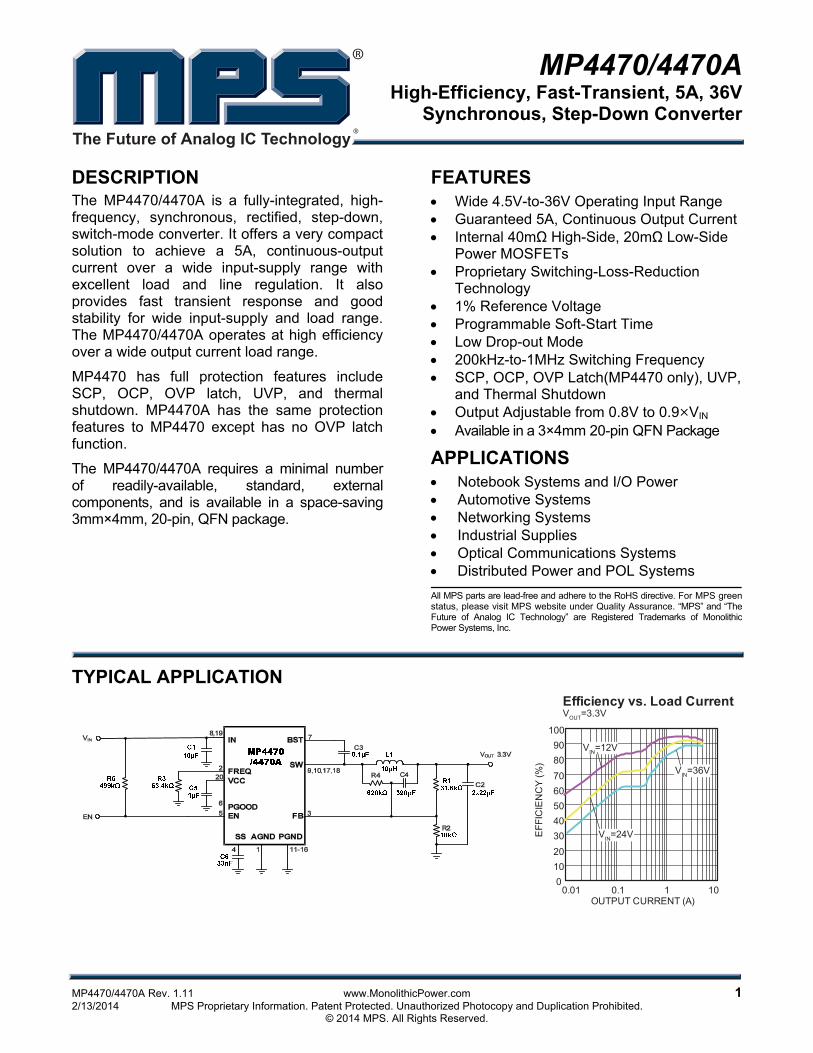
MP4470/4470A High-Efficiency, Fast-Transient, 5A, 36V Synchronous, Step-Down Converter
MP4470/4470A Rev. 1.11 www.MonolithicPower.com 1 2/13/2014 MPS Proprietary Information. Patent Protected. Unauthorized Photocopy and Duplication Prohibited. © 2014 MPS. All Rights Reserved.
The Future of Analog IC Technology
DESCRIPTION The MP4470/4470A is a fully-integrated, high-frequency, synchronous, rectified, step-down, switch-mode converter. It offers a very compact solution to achieve a 5A, continuous-output current over a wide input-supply range with excellent load and line regulation. It also provides fast transient response and good stability for wide input-supply and load range. The MP4470/4470A operates at high efficiency over a wide output current load range.
MP4470 has full protection features include SCP, OCP, OVP latch, UVP, and thermal shutdown. MP4470A has the same protection features to MP4470 except has no OVP latch function.
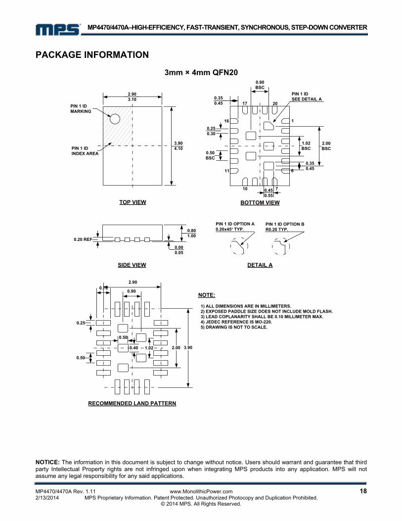
The MP4470/4470A requires a minimal number of readily-available, standard, external components, and is available in a space-saving 3mm×4mm, 20-pin, QFN package.
FEATURES • Wide 4.5V-to-36V Operating Input Range • Guaranteed 5A, Continuous Output Current • Internal 40mΩ High-Side, 20mΩ Low-Side
Power MOSFETs • Proprietary Switching-Loss-Reduction
Technology • 1% Reference Voltage • Programmable Soft-Start Time • Low Drop-out Mode • 200kHz-to-1MHz Switching Frequency • SCP, OCP, OVP Latch(MP4470 only), UVP,
and Thermal Shutdown • Output Adjustable from 0.8V to 0.9×VIN • Available in a 3×4mm 20-pin QFN Package
APPLICATIONS • Notebook Systems and I/O Power • Automotive Systems • Networking Systems • Industrial Supplies • Optical Communications Systems • Distributed Power and POL Systems All MPS parts are lead-free and adhere to the RoHS directive. For MPS green status, please visit MPS website under Quality Assurance. “MPS” and “The Future of Analog IC Technology” are Registered Trademarks of Monolithic Power Systems, Inc.
TYPICAL APPLICATION
0102030405060708090
100
0.01 0.1 1 10OUTPUT CURRENT (A)
MP4470/4470A–HIGH-EFFICIENCY, FAST-TRANSIENT, SYNCHRONOUS, STEP-DOWN CONVERTER
MP4470/4470A Rev. 1.11 www.MonolithicPower.com 2 2/13/2014 MPS Proprietary Information. Patent Protected. Unauthorized Photocopy and Duplication Prohibited. © 2014 MPS. All Rights Reserved.
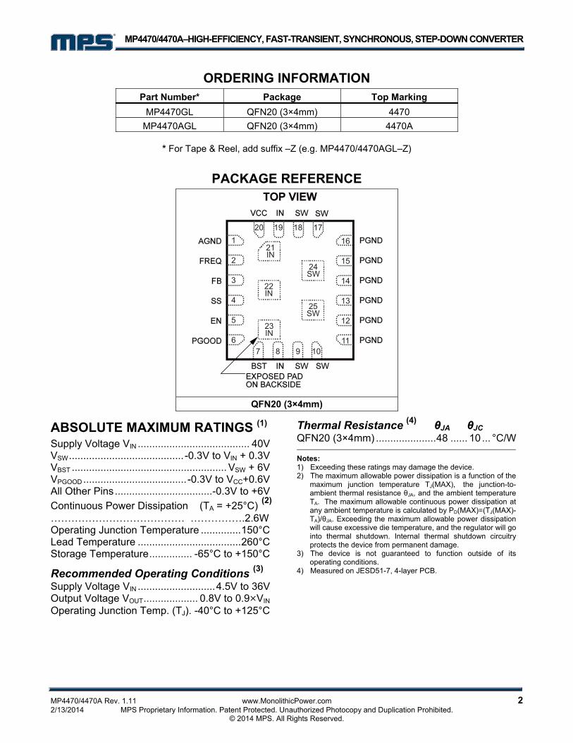
ORDERING INFORMATION Part Number* Package Top Marking
MP4470GL QFN20 (3×4mm) 4470 MP4470AGL QFN20 (3×4mm) 4470A
* For Tape & Reel, add suffix –Z (e.g. MP4470/4470AGL–Z)
PACKAGE REFERENCE
7 8
20 19 18 17
9 10
21IN
22IN
23IN
25SW
24SW
16
15
14
13
12
11
1
2
3
4
5
6
QFN20 (3×4mm)
ABSOLUTE MAXIMUM RATINGS (1) Supply Voltage VIN ....................................... 40V VSW........................................ -0.3V to VIN + 0.3V VBST ...................................................... VSW + 6V VPGOOD .................................... -0.3V to VCC+0.6V All Other Pins..................................-0.3V to +6V Continuous Power Dissipation (TA = +25°C) (2) ………………………………… …………….2.6W Operating Junction Temperature ..............150°C Lead Temperature ....................................260°C Storage Temperature............... -65°C to +150°C
Recommended Operating Conditions (3) Supply Voltage VIN ...........................4.5V to 36V Output Voltage VOUT................... 0.8V to 0.9×VIN Operating Junction Temp. (TJ). -40°C to +125°C
Thermal Resistance (4) θJA θJC QFN20 (3×4mm) .....................48 ...... 10 ... °C/W
Notes: 1) Exceeding these ratings may damage the device. 2) The maximum allowable power dissipation is a function of the
maximum junction temperature TJ(MAX), the junction-to-ambient thermal resistance θJA, and the ambient temperature TA. The maximum allowable continuous power dissipation at any ambient temperature is calculated by PD(MAX)=(TJ(MAX)-TA)/θJA. Exceeding the maximum allowable power dissipation will cause excessive die temperature, and the regulator will go into thermal shutdown. Internal thermal shutdown circuitry protects the device from permanent damage.
3) The device is not guaranteed to function outside of its operating conditions.
4) Measured on JESD51-7, 4-layer PCB.
MP4470/4470A–HIGH-EFFICIENCY, FAST-TRANSIENT, SYNCHRONOUS, STEP-DOWN CONVERTER
MP4470/4470A Rev. 1.11 www.MonolithicPower.com 3 2/13/2014 MPS Proprietary Information. Patent Protected. Unauthorized Photocopy and Duplication Prohibited. © 2014 MPS. All Rights Reserved.
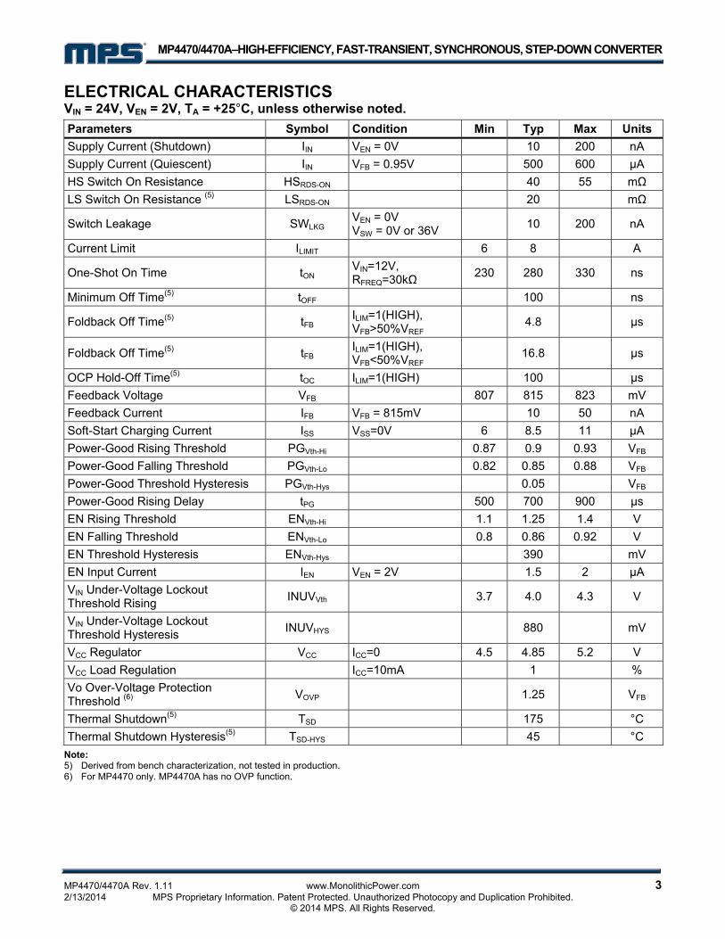
ELECTRICAL CHARACTERISTICS VIN = 24V, VEN = 2V, TA = +25°C, unless otherwise noted. Parameters Symbol Condition Min Typ Max Units Supply Current (Shutdown) IIN VEN = 0V 10 200 nA Supply Current (Quiescent) IIN VFB = 0.95V 500 600 μA HS Switch On Resistance HSRDS-ON 40 55 mΩ LS Switch On Resistance (5) LSRDS-ON 20 mΩ
Switch Leakage SWLKG VEN = 0V VSW = 0V or 36V 10 200 nA
Current Limit ILIMIT 6 8 A
One-Shot On Time tON VIN=12V, RFREQ=30kΩ 230 280 330 ns
Minimum Off Time(5) tOFF 100 ns
Foldback Off Time(5) tFB ILIM=1(HIGH), VFB>50%VREF 4.8 μs
Foldback Off Time(5) tFB ILIM=1(HIGH), VFB<50%VREF 16.8 μs
OCP Hold-Off Time(5) tOC ILIM=1(HIGH) 100 μs
Feedback Voltage VFB 807 815 823 mV Feedback Current IFB VFB = 815mV 10 50 nA Soft-Start Charging Current ISS VSS=0V 6 8.5 11 μA Power-Good Rising Threshold PGVth-Hi 0.87 0.9 0.93 VFB Power-Good Falling Threshold PGVth-Lo 0.82 0.85 0.88 VFB Power-Good Threshold Hysteresis PGVth-Hys 0.05 VFB Power-Good Rising Delay tPG 500 700 900 μs EN Rising Threshold ENVth-Hi 1.1 1.25 1.4 V EN Falling Threshold ENVth-Lo 0.8 0.86 0.92 V EN Threshold Hysteresis ENVth-Hys 390 mV EN Input Current IEN VEN = 2V 1.5 2 μA VIN Under-Voltage Lockout Threshold Rising INUVVth 3.7 4.0 4.3 V
VIN Under-Voltage Lockout Threshold Hysteresis INUVHYS 880 mV
VCC Regulator VCC ICC=0 4.5 4.85 5.2 V VCC Load Regulation ICC=10mA 1 % Vo Over-Voltage Protection Threshold (6) VOVP 1.25 VFB
Thermal Shutdown(5) TSD 175 °C Thermal Shutdown Hysteresis(5) TSD-HYS 45 °C
Note: 5) Derived from bench characterization, not tested in production. 6) For MP4470 only. MP4470A has no OVP function.
MP4470/4470A–HIGH-EFFICIENCY, FAST-TRANSIENT, SYNCHRONOUS, STEP-DOWN CONVERTER
MP4470/4470A Rev. 1.11 www.MonolithicPower.com 4 2/13/2014 MPS Proprietary Information. Patent Protected. Unauthorized Photocopy and Duplication Prohibited. © 2014 MPS. All Rights Reserved.
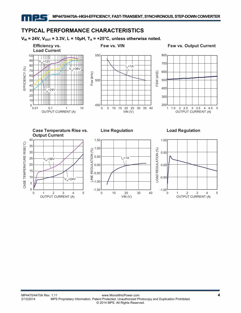
TYPICAL PERFORMANCE CHARACTERISTICS VIN = 24V, VOUT = 3.3V, L = 10µH, TA = +25°C, unless otherwise noted.
Efficiency vs. Load Current
0102030405060708090
100
0.01 0.1 1 10450
500
550
0 5 10 15 20 25 30 35 40VIN (V)
Case Temperature Rise vs. Output Current
0
5
10
15
20
25
30
35
40
0 1 2 3 4 5
Line Regulation
-1.50
-1.00
-0.50
0.00
0.50
1.00
1.50
0 10 20 30 40
Load Regulation
-1.00
-0.50
0.00
0.50
1.00
0 1 2 3 4 5
200
300
400
500
600
700
800
1 1.5 2 2.5 3 3.5 4 4.5 5

MP4470/4470A–HIGH-EFFICIENCY, FAST-TRANSIENT, SYNCHRONOUS, STEP-DOWN CONVERTER
MP4470/4470A Rev. 1.11 www.MonolithicPower.com 5 2/13/2014 MPS Proprietary Information. Patent Protected. Unauthorized Photocopy and Duplication Prohibited. © 2014 MPS. All Rights Reserved.
TYPICAL PERFORMANCE CHARACTERISTICS (CONTINUED) VIN = 24V, VOUT = 3.3V, L = 10µH, TA = +25°C, unless otherwise noted.
VO(AC)10mV/div.
SW10V/div.
IL500mA/div.
VIN10V/div.
VO2V/div.
SW20V/div.
IL2A/div.
VIN10V/div.
VO2V/div.
SW20V/div.
IL5A/div.
VIN10V/div.
VO2V/div.
SW10V/div.
IL200mA/div.
VIN10V/div.
VO2V/div.
SW10V/div.
IL2A/div.
EN2V/div.
VO2V/div.
SW20V/div.
IL500mA/div.
EN2V/div.
VO2V/div.
SW20V/div.
IL5A/div.
EN2V/div.
VO2V/div.
SW20V/div.
IL2A/div.
VO(AC)10mV/div.
SW20V/div.
IL1A/div.

MP4470/4470A–HIGH-EFFICIENCY, FAST-TRANSIENT, SYNCHRONOUS, STEP-DOWN CONVERTER
MP4470/4470A Rev. 1.11 www.MonolithicPower.com 6 2/13/2014 MPS Proprietary Information. Patent Protected. Unauthorized Photocopy and Duplication Prohibited. © 2014 MPS. All Rights Reserved.
TYPICAL PERFORMANCE CHARACTERISTICS (CONTINUED) VIN = 24V, VOUT = 3.3V, L = 10µH, TA = +25°C, unless otherwise noted.
MP4470/4470A–HIGH-EFFICIENCY, FAST-TRANSIENT, SYNCHRONOUS, STEP-DOWN CONVERTER
MP4470/4470A Rev. 1.11 www.MonolithicPower.com 7 2/13/2014 MPS Proprietary Information. Patent Protected. Unauthorized Photocopy and Duplication Prohibited. © 2014 MPS. All Rights Reserved.
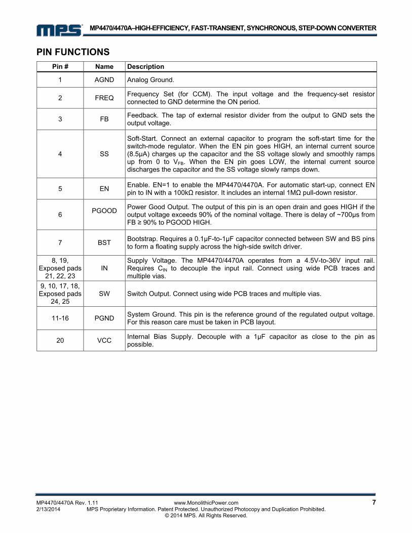
PIN FUNCTIONS Pin # Name Description
1 AGND Analog Ground.
2 FREQ Frequency Set (for CCM). The input voltage and the frequency-set resistor connected to GND determine the ON period.
3 FB Feedback. The tap of external resistor divider from the output to GND sets the output voltage.
4 SS
Soft-Start. Connect an external capacitor to program the soft-start time for the switch-mode regulator. When the EN pin goes HIGH, an internal current source (8.5µA) charges up the capacitor and the SS voltage slowly and smoothly ramps up from 0 to VFB. When the EN pin goes LOW, the internal current source discharges the capacitor and the SS voltage slowly ramps down.
5 EN Enable. EN=1 to enable the MP4470/4470A. For automatic start-up, connect EN pin to IN with a 100kΩ resistor. It includes an internal 1MΩ pull-down resistor.
6 PGOOD
Power Good Output. The output of this pin is an open drain and goes HIGH if the output voltage exceeds 90% of the nominal voltage. There is delay of ~700µs from FB ≥ 90% to PGOOD HIGH.
7 BST Bootstrap. Requires a 0.1µF-to-1µF capacitor connected between SW and BS pins to form a floating supply across the high-side switch driver.
8, 19, Exposed pads
21, 22, 23 IN
Supply Voltage. The MP4470/4470A operates from a 4.5V-to-36V input rail. Requires CIN to decouple the input rail. Connect using wide PCB traces and multiple vias.
9, 10, 17, 18, Exposed pads
24, 25 SW Switch Output. Connect using wide PCB traces and multiple vias.
11-16 PGND System Ground. This pin is the reference ground of the regulated output voltage. For this reason care must be taken in PCB layout.
20 VCC Internal Bias Supply. Decouple with a 1µF capacitor as close to the pin as possible.
MP4470/4470A–HIGH-EFFICIENCY, FAST-TRANSIENT, SYNCHRONOUS, STEP-DOWN CONVERTER
MP4470/4470A Rev. 1.11 www.MonolithicPower.com 8 2/13/2014 MPS Proprietary Information. Patent Protected. Unauthorized Photocopy and Duplication Prohibited. © 2014 MPS. All Rights Reserved.
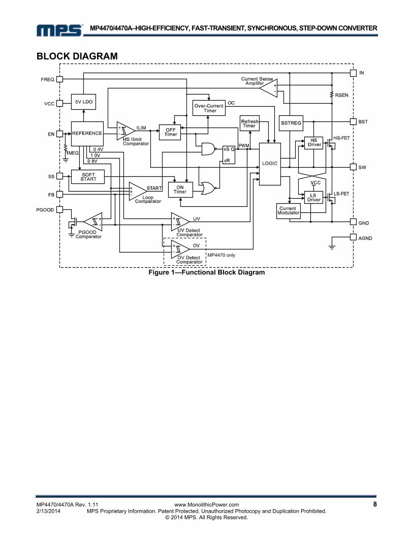
BLOCK DIAGRAM
Figure 1—Functional Block Diagram
MP4470/4470A–HIGH-EFFICIENCY, FAST-TRANSIENT, SYNCHRONOUS, STEP-DOWN CONVERTER
MP4470/4470A Rev. 1.11 www.MonolithicPower.com 9 2/13/2014 MPS Proprietary Information. Patent Protected. Unauthorized Photocopy and Duplication Prohibited. © 2014 MPS. All Rights Reserved.
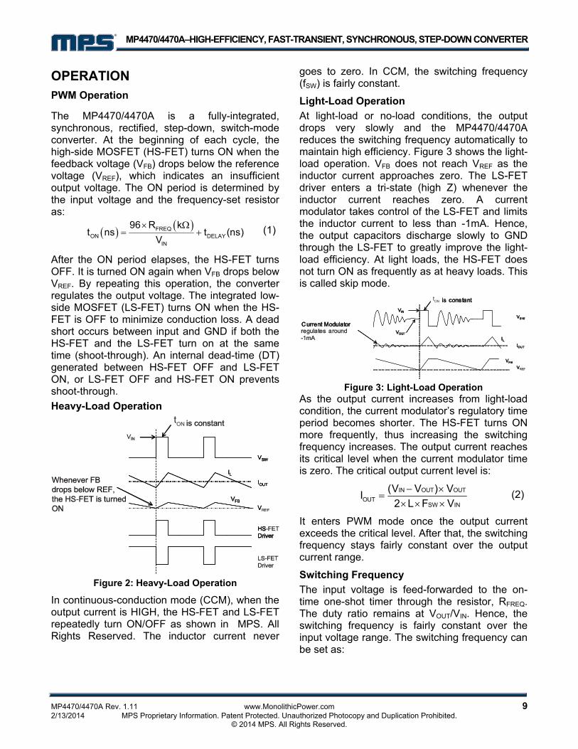
OPERATION PWM Operation
The MP4470/4470A is a fully-integrated, synchronous, rectified, step-down, switch-mode converter. At the beginning of each cycle, the high-side MOSFET (HS-FET) turns ON when the feedback voltage (VFB) drops below the reference voltage (VREF), which indicates an insufficient output voltage. The ON period is determined by the input voltage and the frequency-set resistor as:
( ) ( )FREQON DELAY
IN
96 R kt ns t (ns)
V× Ω
= + (1)
After the ON period elapses, the HS-FET turns OFF. It is turned ON again when VFB drops below VREF. By repeating this operation, the converter regulates the output voltage. The integrated low-side MOSFET (LS-FET) turns ON when the HS-FET is OFF to minimize conduction loss. A dead short occurs between input and GND if both the HS-FET and the LS-FET turn on at the same time (shoot-through). An internal dead-time (DT) generated between HS-FET OFF and LS-FET ON, or LS-FET OFF and HS-FET ON prevents shoot-through. Heavy-Load Operation
tON
Figure 2: Heavy-Load Operation
In continuous-conduction mode (CCM), when the output current is HIGH, the HS-FET and LS-FET repeatedly turn ON/OFF as shown in MPS. All Rights Reserved. The inductor current never
goes to zero. In CCM, the switching frequency (fSW) is fairly constant.
Light-Load Operation At light-load or no-load conditions, the output drops very slowly and the MP4470/4470A reduces the switching frequency automatically to maintain high efficiency. Figure 3 shows the light-load operation. VFB does not reach VREF as the inductor current approaches zero. The LS-FET driver enters a tri-state (high Z) whenever the inductor current reaches zero. A current modulator takes control of the LS-FET and limits the inductor current to less than -1mA. Hence, the output capacitors discharge slowly to GND through the LS-FET to greatly improve the light-load efficiency. At light loads, the HS-FET does not turn ON as frequently as at heavy loads. This is called skip mode.
tON
Figure 3: Light-Load Operation
As the output current increases from light-load condition, the current modulator’s regulatory time period becomes shorter. The HS-FET turns ON more frequently, thus increasing the switching frequency increases. The output current reaches its critical level when the current modulator time is zero. The critical output current level is:
IN OUT OUTOUT
SW IN
(V V ) VI2 L F V
− ×=
× × × (2)
It enters PWM mode once the output current exceeds the critical level. After that, the switching frequency stays fairly constant over the output current range.
Switching Frequency The input voltage is feed-forwarded to the on-time one-shot timer through the resistor, RFREQ. The duty ratio remains at VOUT/VIN. Hence, the switching frequency is fairly constant over the input voltage range. The switching frequency can be set as:

MP4470/4470A–HIGH-EFFICIENCY, FAST-TRANSIENT, SYNCHRONOUS, STEP-DOWN CONVERTER
MP4470/4470A Rev. 1.11 www.MonolithicPower.com 10 2/13/2014 MPS Proprietary Information. Patent Protected. Unauthorized Photocopy and Duplication Prohibited. © 2014 MPS. All Rights Reserved.
6
SWFREQ IN
DELAYIN OUT
10F (kHz)96 R (k ) V[ t (ns)]
V V
=× Ω
+ × (3)
Where tDELAY is the comparator delay (~20ns).
The MP4470/4470A is optimized for 200kHz-to-1MHz applications to operate at high switching frequencies with high efficiency. The high-switching frequency allows for smaller LC-filter components to reduce PCB space requirements.
Ramp Compensation Figure 4 and Figure 5 show jitter occurring in both PWM mode and skip mode. Noise on VFB’s downward slope causes the HS-FET ON time to deviate from its intended position and produces jitter. There is a relationship between system stability and the steepness of the VFB ripple: The slope steepness of the VFB ripple dominates noise immunity. The magnitude of the VFB ripple doesn’t affect the noise immunity directly.
Figure 4: Jitter in PWM Mode
Figure 3: Jitter in Skip Mode
Ceramic output capacitors lack enough ESR ripple to stabilize the system, and requires an external compensation ramp.
IC4
IFB
IIR4
IFB
Figure 6: Simplified Circuit in PWM Mode with
External Ramp Compensation In PWM mode has an equivalent circuit with HS-FET OFF and uses a external ramp compensation circuit (R4, C4), shown as a simplified circuit in Figure 6. Derive the external ramp from the inductor-ripple current. Choose C4, R1, and R2 to meet the following condition:
1 2
SW 4 1 2
R R1 12 F C 5 R R
⎛ ⎞×< × ⎜ ⎟π× × +⎝ ⎠
(4)
Then:
R4 C4 FB C4I I I I= + ≈ (5)
The VFB downward slope ripple is then estimated as:
OUTSLOPE1
4 4
VVR C−
=×
(6)
From equation 6, reduce R4 or C4 to reduce instability in PWM mode. If C4 cannot be reduced further due to equation 4’s limitations, then only reduce R4. Based on bench experiments, VSLOPE1 is around 20V/ms-40V/ms.
In the case of POSCAP or other types of capacitors with higher ESR, an external ramp is not necessary.
Figure 7: Simplified Circuit in PWM Mode without
External Ramp Compensation

MP4470/4470A–HIGH-EFFICIENCY, FAST-TRANSIENT, SYNCHRONOUS, STEP-DOWN CONVERTER
MP4470/4470A Rev. 1.11 www.MonolithicPower.com 11 2/13/2014 MPS Proprietary Information. Patent Protected. Unauthorized Photocopy and Duplication Prohibited. © 2014 MPS. All Rights Reserved.
Figure 7 shows an equivalent circuit in PWM mode with the HS-FET OFF and without an external ramp circuit. The ESR ripple dominates the output ripple. The VFB downward slope is:
REFSLOPE1
ESR VVL
− ×= (7)
From equation 7, the VFB downward slope is proportional to ESR/L. Therefore, it’s necessary to know the minimum ESR value of the output capacitors without an external ramp. There is also an inductance limit: A smaller inductance leads to more stability. Based on bench experiments, keep VSLOPE1 around 15V/ms to 30V/ms.
In skip mode, the external ramp does not affect the downward slope, and VFB ripple’s downward slope is the same with or without the external ramp. Figure 8 shows an equivalent circuit with the HS-FET off and the current modulator regulating the LS-FET.
IMOD
Figure 8: Simplified Circuit in Skip Mode
The VFB ripple’s downward slope is:
( )
−=
+ ×REF
SLOPE21 2 OUT
VVR R C
(8)
To keep the system stable during light loads, avoid large VFB resistors. Also, keep the VSLOPE2 value around 0.4V/ms to 0.8mV/ms. Note that IMOD is excluded from the equation because it does not impact the system’s light-load stability.
Soft-Start The MP4470/4470A employs soft start (SS) to ensure a smooth output during power-up. When the EN pin goes HIGH, an internal current source (8.5μA) charges up the SS capacitor (CSS). The CSS voltage takes over the REF voltage to the PWM comparator. The output voltage smoothly
ramps up with VSS. Once VSS reaches the same level as VREF, it continues ramping up while VREF takes over the PWM comparator. At this point, soft-start finishes and the MP4470/4470A enters steady-state.
CSS is then:
( ) ( ) ( )( )
SS SSSS
REF
t ms I AC nF
V V× μ
= (9)
If the output capacitors have large capacitance values, avoid setting a short SS or risk hitting the current limit during SS. Select a minimum value of 4.7nF if the output capacitance value exceeds 330μF.
Power Good (PGOOD) The MP4470/4470A has power-good (PGOOD) output. The PGOOD pin is the open drain of a MOSFET. It should connect to VCC or some other voltage source through a resistor (e.g. 100kΩ). In the presence of an input voltage, the MOSFET turns ON so that the PGOOD pin is pulled to GND before SS is ready. After VFB reaches 90%×VREF, the PGOOD pin is pulled HIGH after a delay; typically 700μs.
When the FB voltage drops to 85%×VREF, the PGOOD pin is pulled LOW.
Over-Current Protection (OCP) and Short-Circuit Protection (SCP) The MP4470/4470A has cycle-by-cycle over-current limit control. The inductor current is monitored during the ON state. Once the inductor current exceeds the current limit, the HS-FET turns OFF. At the same time, the OCP timer starts. The OCP timer is set at 100μs. Hitting the current limit during each cycle during this 100μs time frame will trigger hiccup SCP.
If a short circuit occurs, the MP4470/4470A will immediately hit its current limit and VFB will drop below 50%×VREF (0.815V). The device considers this an output dead short and will trigger hiccup SCP immediately.
Over/Under-Voltage Protection (OVP/UVP) The MP4470 monitors the output voltage through the tap of a resistor divider to the FB pin to detect output over-voltage conditions. A VFB that exceeds 125%×VREF (0.815V) triggers OVP latch-off. Once OVP triggers, the LS-FET turns on to discharge VO until the inductor current drops to

MPS C
ONFIDENTIA
L
DO NOT D
ISTRIB
UTE
MPS C
ONFIDENTIA
L
DO NOT D
ISTRIB
UTE
MPS C
ONFIDENTIA
L
DO NOT D
ISTRIB
UTE
MP4470/4470A–HIGH-EFFICIENCY, FAST-TRANSIENT, SYNCHRONOUS, STEP-DOWN CONVERTER
MPS CONFIDENTIAL AND PROPRIETARY INFORMATION – INTERNAL USE ONLY
MP4470/4470A Rev.0.8 www.MonolithicPower.com 12 2/13/2014 MPS Proprietary Information. Patent Protected. Unauthorized Photocopy and Duplication Prohibited. Preliminary Specifications Subject to Change © 2014 MPS. All Rights Reserved.
zero while the HS-FET remains off. The MP4470 needs to power cycle to restart. Note that MP4470A has no this OVP function.
The MP4470/4470A also monitors FB pin voltage to detect output under-voltage condition. A VFB drop below 50% ×VREF triggers UVP as well as a current-limit that triggers SCP.
UVLO Protection The MP4470/4470A has under-voltage lock-out protection (UVLO). When the input voltage is higher than the UVLO rising threshold voltage, the MP4470/4470A will be powered up. It shuts off when the input voltage is lower than the UVLO falling threshold voltage. This is non-latch protection.
Floating Driver and Bootstrap Charging An external bootstrap capacitor power the floating-power-MOSFET driver. A dedicated internal regulator charges and regulates the bootstrap capacitor voltage to ~5V. When the voltage between the BST and SW nodes drops below regulation, a PMOS pass transistor connected from VIN to BST turns on. The charging current path is from VIN, BST and then to SW. The external circuit should provide enough voltage headroom to facilitate charging.
As long as VIN is significantly higher than SW, the bootstrap capacitor remains charged. When the HS-FET is ON, VIN≈VSW so the bootstrap capacitor cannot charge.
When the LS-FET is ON, VIN−VSW reaches its maximum for fast charging. When there is no inductor current, VSW=VOUT so the difference between VIN and VOUT can charge the bootstrap capacitor.
At higher duty cycles, the bootstrap-charging time is shorter so the bootstrap capacitor may not charge sufficiently. In case the internal circuit has insufficient voltage and time to charge the bootstrap capacitor, the bootstrap capacitor voltage will drop low. When VBST−VSW drops below 2.3V, the HS-FET turns OFF. A UVLO circuit allows the LS-FET to conduct and refresh the charge on the bootstrap capacitor. Once bootstrap capacitor voltage is charged, the HS-FET can turn on again and the part resumes normal switching. With this bootstrap refreshing function, MP4470/4470A is able to work on the low drop-out mode.
Thermal Shutdown The MP4470/4470A uses thermal shutdown. The junction temperature of the IC is internally monitored. If the junction temperature exceeds the threshold value (typically 175°C), the converter shuts off. This is a non-latched protection. There is about 45°C hysteresis. Once the junction temperature drops to about 130°C, it initiates a SS.

MP4470/4470A–HIGH-EFFICIENCY, FAST-TRANSIENT, SYNCHRONOUS, STEP-DOWN CONVERTER
MP4470/4470A Rev. 1.11 www.MonolithicPower.com 13 2/13/2014 MPS Proprietary Information. Patent Protected. Unauthorized Photocopy and Duplication Prohibited. © 2014 MPS. All Rights Reserved.
APPLICATION INFORMATION Setting the Output Voltage A resistor divider from the output voltage to the FB pin set VOUT.
Without an external ramp employed, the feedback resistors (R1 and R2) set the output voltage. To determine the values for the resistors, first, choose R2 (typically 5kΩ-40kΩ). Then R1 is:
OUT REF
REF
V VR1 R2V−
= × (10)
When using a low-ESR ceramic capacitor on the output, add an external voltage ramp to the FB pin through R4 and C4. The ramp voltage (VRAMP) affects output voltage. Calculate VRAMP as per equation 19. Choose R2 between 5kΩ and 40kΩ. Determine R1 as:
1
42
11
21
21 −
⎟⎟⎟⎟
⎠
⎞
⎜⎜⎜⎜
⎝
⎛
−−−×
+=
R)VVV(R
VVR
RAMPREFOUT
RAMPREF(11)
Using equation 11 to calculate the output voltage can be complicated. Furthermore, as VRAMP changes due to changes in VOUT and VIN, VFB also varies. To improve the output voltage accuracy and simplify the R2 calculation from equation 11, add a DC-blocking capacitor (CDC). Figure 9 shows a simplified circuit with external ramp compensation and a DC-blocking capacitor. Equation 10 can then estimate R1)
Select a CDC value between 1µF and 4.7μF to improve DC-blocking performance.
Cdc
Figure 9: Simplified Circuit with External Ramp
Compensation and DC Blocking Capacitor
Input Capacitor The input current to the step-down converter is discontinuous, and Therefore requires a capacitor to supply the AC current to the step-down converter while maintaining the DC input voltage. Ceramic capacitors are recommended for best performance. Be sure to place the input capacitors as close to the IN pin as possible.
The capacitance varies significantly with temperature. Capacitors with X5R and X7R ceramic dielectrics are are fairly stable over temperature fluctuations.
The capacitors must also have a ripple-current rating greater than the converter’s maximum input-ripple current. The input ripple current can be estimated as follows:
OUT OUTCIN OUT
IN IN
V VI I (1 )V V
= × × − (12)
The worst-case condition occurs at VIN = 2VOUT, where:
OUTCIN
II2
= (13)
For simplification, choose an input capacitor whose RMS current rating is greater than half of the maximum load current.The input capacitance value determines the input voltage ripple of the converter. If there is an input-voltage-ripple requirement in the system design, choose an input capacitor that meets the specification
The input voltage ripple can be estimated as follows:
OUT OUT OUTIN
SW IN IN IN
I V VV (1 )F C V V
Δ = × × −×
(14)
The worst-case condition occurs at VIN = 2VOUT, where:
OUTIN
SW IN
I1V4 F C
Δ = ××
(15)
MP4470/4470A–HIGH-EFFICIENCY, FAST-TRANSIENT, SYNCHRONOUS, STEP-DOWN CONVERTER
MP4470/4470A Rev. 1.11 www.MonolithicPower.com 14 2/13/2014 MPS Proprietary Information. Patent Protected. Unauthorized Photocopy and Duplication Prohibited. © 2014 MPS. All Rights Reserved.
Output Capacitor The output capacitor maintains the DC output voltage. Use ceramic or POSCAP capacitors. The output voltage ripple can be estimated as: OUT OUT
OUT ESRSW IN SW OUT
V V 1V (1 ) (R )F L V 8 F C
Δ = × − × +× × ×
(16)
Where RESR is the equivalent series resistance of the output capacitor.
For ceramic capacitors, capacitance dominates the impedance at the switching frequency, can is the primary cause of the output-voltage ripple. For simplification, estimate the output voltage ripple as:
OUT OUTOUT 2
SW OUT IN
V VV (1 )8 F L C V
Δ = × −× × ×
(17)
The output voltage ripple caused by ESR is very small and therefore requires an external ramp to stabilize the system. The voltage ramp is ~30mV. The external ramp can be generated through R4 and C4 using the following equation:
IN OUT ONRAMP
(V V ) TVR4 C4− ×
=×
(18)
Select C4 to meet the following condition:
SW
R1 R21 1 ( )2 F C4 5 R1 R2
×< ×
π× × + (19)
For POSCAP capacitors, the ESR dominates the impedance at the switching frequency. The ramp voltage generated from the ESR is high enough to stabilize the system. Therefore, an external ramp is not needed. A minimum ESR value of 12mΩ is required to ensure stable operation of the converter. For simplification, the output ripple can be approximated as:
OUT OUTOUT ESR
SW IN
V VV (1 ) RF L V
Δ = × − ××
(20)
Inductor The inductor is required to supply constant current to the output load while being driven by the switching input voltage. A larger inductance will result in less ripple current and a lower output ripple voltage. However, a larger inductance resultsin a larger inductor, which will physically larger, and have a higher series resistance and/or lower saturation current. A good rule for determining the inductor value is to allow the peak-to-peak ripple current in the inductor to be approximately 30% to 40% of the maximum switch current limit. Ensure that the peak inductor current is below the maximum switch current limit. The inductance value can be calculated as:
OUT OUT
SW L IN
V VL (1 )F I V
= × −×Δ
(21)
Where ΔIL is the peak-to-peak inductor ripple current.
Choose an inductor that will not saturate under the maximum inductor peak current. The peak inductor current can be calculated as:
OUT OUT
LP OUTSW IN
V VI I (1 )2F L V
= + × −× (22)
MP4470/4470A–HIGH-EFFICIENCY, FAST-TRANSIENT, SYNCHRONOUS, STEP-DOWN CONVERTER
MP4470/4470A Rev. 1.11 www.MonolithicPower.com 15 2/13/2014 MPS Proprietary Information. Patent Protected. Unauthorized Photocopy and Duplication Prohibited. © 2014 MPS. All Rights Reserved.
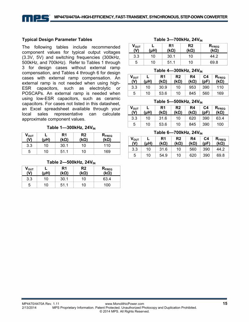
Typical Design Parameter Tables The following tables include recommended component values for typical output voltages (3.3V, 5V) and switching frequencies (300kHz, 500kHz, and 700kHz). Refer to Tables 1 through 3 for design cases without external ramp compensation, and Tables 4 through 6 for design cases with external ramp compensation. An external ramp is not needed when using high-ESR capacitors, such as electrolytic or POSCAPs. An external ramp is needed when using low-ESR capacitors, such as ceramic capacitors. For cases not listed in this datasheet, an Excel spreadsheet available through your local sales representative can calculate approximate component values.
Table 1—300kHz, 24VIN VOUT (V)
L (μH)
R1 (kΩ)
R2 (kΩ)
RFREQ (kΩ)
3.3 10 30.1 10 110 5 10 51.1 10 169
Table 2—500kHz, 24VIN VOUT (V)
L (μH)
R1 (kΩ)
R2 (kΩ)
RFREQ (kΩ)
3.3 10 30.1 10 63.4 5 10 51.1 10 100
Table 3—700kHz, 24VIN VOUT (V)
L (μH)
R1 (kΩ)
R2 (kΩ)
RFREQ (kΩ)
3.3 10 30.1 10 44.2 5 10 51.1 10 69.8
Table 4—300kHz, 24VIN VOUT(V)
L (μH)
R1 (kΩ)
R2 (kΩ)
R4 (kΩ)
C4 (pF)
RFREQ(kΩ)
3.3 10 30.9 10 953 390 110 5 10 53.6 10 845 560 169
Table 5—500kHz, 24VIN VOUT(V)
L (μH)
R1 (kΩ)
R2 (kΩ)
R4 (kΩ)
C4 (pF)
RFREQ(kΩ)
3.3 10 31.6 10 620 390 63.4 5 10 53.6 10 845 390 100
Table 6—700kHz, 24VIN VOUT(V)
L (μH)
R1 (kΩ)
R2 (kΩ)
R4 (kΩ)
C4 (pF)
RFREQ(kΩ)
3.3 10 31.6 10 560 390 44.2 5 10 54.9 10 620 390 69.8

MP4470/4470A–HIGH-EFFICIENCY, FAST-TRANSIENT, SYNCHRONOUS, STEP-DOWN CONVERTER
MP4470/4470A Rev. 1.11 www.MonolithicPower.com 16 2/13/2014 MPS Proprietary Information. Patent Protected. Unauthorized Photocopy and Duplication Prohibited. © 2014 MPS. All Rights Reserved.
LAYOUT RECOMMENDATION 1. Place high-current paths (GND, IN, and SW)
very close to the device with short, direct, and wide traces.
2. Place input capacitors on both VIN sides (PIN8 and PIN19) and as close to the IN and GND pins as possible.
3. Place the decoupling capacitor as close to the VCC and GND pins as possible.
4. Keep the switching node SW short and away from the feedback network.
5. Place the external feedback resistors next to the FB pin. Do not place vias on the FB trace.
6. Keep the BST voltage path (BST, C3, and SW) as short as possible.
7. Connect the bottom IN and SW pads to a large copper area to achieve better thermal performance.
8. A Four-layer layout is strongly recommended to achieve better thermal performance.
C1A
C1B
C1C
C2A
C2B
Top Layer
Inner1 Layer
Inner2 Layer
Bottom Layer
Figure 10: PCB Layout

MP4470/4470A–HIGH-EFFICIENCY, FAST-TRANSIENT, SYNCHRONOUS, STEP-DOWN CONVERTER
MP4470/4470A Rev. 1.11 www.MonolithicPower.com 17 2/13/2014 MPS Proprietary Information. Patent Protected. Unauthorized Photocopy and Duplication Prohibited. © 2014 MPS. All Rights Reserved.
TYPICAL APPLICATION CIRCUITS
499kO
63.4kO
10礔
1礔
33nF
0.1礔
10礖
390pF620kO
10kO
31.6kO 22礔
L1
R1
C1B
R3
4.7OR5
C6
C5
R7R6
100kO
10礔C1A
22礔C2BC2A
3.3V
SS AGND PGNDVCC
PGOOD
FREQ
EN
FB
SW
BSTVINMP4470/4470A
8,19,21,22,23
5
2
6
20
4 1 11-16
3
9,10,1718,24,25
7
C3
R4 C4
R2
ENVOUT
VIN
0.1礔C1D
0.1礔C1C
0.1礔C2C
Figure 11: Typical Application Circuit, 3.3V-Output
MP4470/4470A–HIGH-EFFICIENCY, FAST-TRANSIENT, SYNCHRONOUS, STEP-DOWN CONVERTER
NOTICE: The information in this document is subject to change without notice. Users should warrant and guarantee that third party Intellectual Property rights are not infringed upon when integrating MPS products into any application. MPS will not assume any legal responsibility for any said applications.
MP4470/4470A Rev. 1.11 www.MonolithicPower.com 18 2/13/2014 MPS Proprietary Information. Patent Protected. Unauthorized Photocopy and Duplication Prohibited. © 2014 MPS. All Rights Reserved.
PACKAGE INFORMATION
3mm × 4mm QFN20