Embed Size (px)
Citation preview

TIST CS 305 MICROPROCESSOR AND MICROCONTROLLERS MODULE IV
Department of CSE Page 1
MODULE 4 Interfacing Memory, I/O, 8255 - Detailed study - Architecture, Control word format and modes of operation, Architecture and modes of operation of 8279 and 8257 (Just mention the control word, no need to memorize the control word format)
MODULE 4 Semiconductor Memory Interfacing: Semiconductor memories are of two types, viz. RAM (Random Access Memory) and ROM (Read Only Memory). Static RAM Interfacing: Q. Explain the general procedure of static memory interfacing with 8086?
The semiconductor RAMs are of broadly two types-static RAM and dynamic RAM. The semiconductor memories are organized as two dimensional arrays of memory locations. For example, 4K x 8 or 4K byte memory contains 4096 locations, where each location contains 8-bit data and only one of the 4096 locations can be selected at a time. Obviously, for addressing 4K bytes of memory, twelve address lines are required. In general, to address a memory location out of N memory locations , we will require at least n bits of address, i.e. n address lines where n = Log2 N. Thus if the microprocessor has n address lines, then it is able to address at the most N locations of memory, where 2n = N. However, if out of N locations only P memory locations are to be interfaced, then the least significant p address lines out of the available n lines can be directly connected from the microprocessor to the memory chip while the remaining (n-p) higher order address lines may be used for address decoding (as inputs to the chip selection logic). The memory address depends upon the hardware circuit used for decoding the chip select (CS). The output of the decoding circuit is connected with the CS pin of the memory chip. The general procedure of static memory interfacing with 8086 is briefly described as follows: 1. Arrange the available memory chips so as to obtain 16-bit data bus width. The upper 8-bit bank is called ‘odd address memory bank’ and the lower 8-bit bank is called ‘even address memory bank’. 2. Connect available memory address lines of memory chips with those of the microprocessor and also connect the memory RD and WR inputs to the corresponding processor control signals. Connect the 16-bit data bus of the memory bank with that of the microprocessor 8086. 3. The remaining address lines of the microprocessor, BHE and A0 are used for decoding the required chip select signals for the odd and even memory banks. CS of memory is derived from the O/P of the decoding circuit .

TIST CS 305 MICROPROCESSOR AND MICROCONTROLLERS MODULE IV
Department of CSE Page 2
As a good and efficient interfacing practice, the address map of the system should be continuous as far as possible, i.e. there should be no windows in the map. A memory location should have a single address corresponding to it, i.e. absolute decoding should be preferred, and minimum hardware should be used for decoding. In a number of cases, linear decoding may be used to minimise the required hardware. Let us now consider a few example problems on memory interfacing with 8086.

TIST CS 305 MICROPROCESSOR AND MICROCONTROLLERS MODULE IV
Department of CSE Page 3

TIST CS 305 MICROPROCESSOR AND MICROCONTROLLERS MODULE IV
Department of CSE Page 4

TIST CS 305 MICROPROCESSOR AND MICROCONTROLLERS MODULE IV
Department of CSE Page 5

TIST CS 305 MICROPROCESSOR AND MICROCONTROLLERS MODULE IV
Department of CSE Page 6
Q.A circuit containing 32KB of RAMis to be interfaced to an 8086 based system, so that the first address of the RAM is at 48000H .What is the entire range of the RAM address ?What address lines should be used?
ANS:
32 KB=25x210=215
So range of address could be
A19 A18 A17 A16 A15 A14 A13 A12 A11 A10 A9 A8 A7 A6 A5 A4 A3 A2 A1 A0 0 1 0 0 1 1 1 1 1 1 1 1 1 1 1 1 1 1 1 1
RAM 0 1 0 0 1 0 0 0 0 0 0 0 0 0 0 0 0 0 0 0
Ie 48000H to 4FFFFH
Q.Give an interfacing circuit to interface a 2K bytes of EPROM and four 2K bytes of RAM to 8086.Starting address of EPROM is 00000H and that of RAM is 60000H.Give memory map of your system and Explain the chip select logic?
ANS:
ROM= 2KB (Addr lines needed=11)
RAM=four 2KB RAM’s=8KB RAM (Addr lines needed=13)
Address Map

TIST CS 305 MICROPROCESSOR AND MICROCONTROLLERS MODULE IV
Department of CSE Page 7
Address
A19
A18
A17
A16
A15
A14
A13
A12
A11
A10
A9
A8
A7
A6
A5
A4
A3
A2
A1
A0
007FF
0 0 0 0 0 0 0 0 0 1 1 1 1 1 1 1 1 1 1 1
ROM 00000
0 0 0 0 0 0 0 0 0 0 0 0 0 0 0 0 0 0 0 0
61FFF
0 1 1 0 0 0 0 1 1 1 1 1 1 1 1 1 1 1 1 1
RAM 60000
0 1 1 0 0 0 0 0 0 0 0 0 0 0 0 0 0 0 0
Q.Design memory interfacing circuit for interfacing 4Kx8 RAM and 2Kx8 Rom using 3 to 8 decorder?(Kerala university) ANS: Split 4Kx8 RAM into two 2Kx8 Chips and
Dynamic RAM Interfacing
Q.Write the advantages of dynamic RAM interfacing?
Q.What do you mean by refresh cycle in dynamic RAM ?
Q.Explain the use of dynamic RAM controller in interfacing DRAM with 8086?

TIST CS 305 MICROPROCESSOR AND MICROCONTROLLERS MODULE IV
Department of CSE Page 8
Whenever a large capacity memory is required in a microcomputer system, the memory subsystem is generally designed using dynamic RAM because there are various advantages of dynamic RAM.
• E.g. higher packing density, lower cost and less power consumption. A typical static RAM cell may require six transistors while the dynamic RAM cell requires only a transistors along with a capacitor. Hence it is possible to obtain higher packaging density and hence low cost units are available.
• The basic dynamic RAM cell uses a capacitor to store the charge as a representation of data. This capacitor is manufactured as a diode that is reverse biased so that the storage capacitance comes into the picture.
• This storage capacitance is utilized for storing the charge representation of data but the reverse-biased diode has leakage current that tends to discharge the capacitor giving rise to the possibility of data loss. To avoid this possible data loss, the data stored in a dynamic RAM cell must be refreshed after a fixed time interval regularly. The process of refreshing the data in RAM is called as Refresh cycle.
• The refresh activity is similar to reading the data from each and every cell of memory, independent of the requirement of microprocessor. During this refresh period all other operations related to the memory subsystem are suspended. Hence the refresh activity causes loss of time, resulting in reduces system performance.
• However keeping in view the advantages of dynamic RAM, like low power consumption, high packaging density and low cost, most of the advanced computing system are designed using dynamic RAM, at the cost of operating speed.
• A dedicated hardware chip called as dynamic RAM controller is the most important part of the interfacing circuit.
The Refresh cycle is different from the memory read cycle in the following aspects.
1. The memory address is not provided by the CPU address bus, rather it is generated by a refresh mechanism counter called as refresh counter.
2. Unlike memory read cycle, more than one memory chip may be enabled at a time so as to reduce the number of total memory refresh cycles.
3. The data enable control of the selected memory chip is deactivated, and data is not allowed to appear on the system data bus during refresh, as more than one memory units are refreshed simultaneously. This is to avoid the data from the different chips to appear on the bus simultaneously.
4. Memory read is either a processor initiated or an external bus master initiated and carried out by the refresh mechanism.

TIST CS 305 MICROPROCESSOR AND MICROCONTROLLERS MODULE IV
Department of CSE Page 9
• Dynamic RAM is available in units of several kilobits to megabits of memory. This memory is arranged internally in a two dimensional matrix array so that it will have n rows and m columns. The row address n and column address m are important for the refreshing operation.
• For example, a typical 4K bit dynamic RAM chip has an internally arranged bit array of dimension 64 * 64 , i.e. 64 rows and 64 columns. The row address and column address will require 6 bits each. These 6 bits for each row address and column address will be generated by the refresh counter, during the refresh cycles.
• A complete row of 64 cells is refreshed at a time to minimizes the refreshing time. Thus the refresh counter needs to generate only row addresses. The row address are multiplexed, over lower order address lines.
• The refresh signals act to control the multiplexer, i.e. when refresh cycle is in process the refresh counter puts the row address over the address bus for refreshing. Otherwise, the address bus of the processor is connected to the address bus of DRAM, during normal processor initiated activities.
• A timer, called refresh timer, derives a pulse for refreshing action after each refresh interval.
• Refresh interval can be qualitatively defined as the time for which a dynamic RAM cell can hold data charge level practically constant, i.e. no data loss takes place.
• Suppose the typical dynamic RAM chip has 64 rows, then each row should be refreshed after each refresh interval or in other words, all the 64 rows are to refreshed in a single refresh interval.
• This refresh interval depends upon the manufacturing technology of the dynamic RAM cell. It may range anywhere from 1ms to 3ms.
• Let us consider 2ms as a typical refresh time interval. Hence, the frequency of the refresh pulses will be calculated as follows:
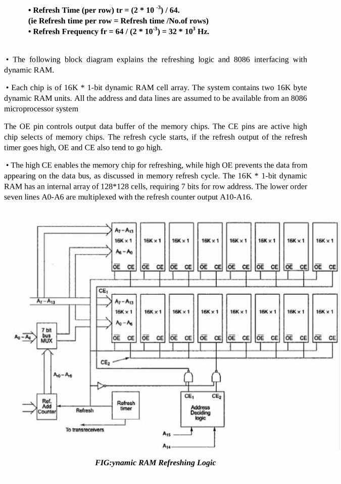
• Refresh Time (per row) tr = (2 * 10 -3) / 64.
(ie Refresh time per row = Refresh time /No.of rows)
• Refresh Frequency fr = 64 / (2 * 10-3) = 32 * 103 Hz.
Problem
A 4k bit dynamic RAM with 2 ms of refresh time interval. find the refresh frequency of the RAM? Solution: A typical 4K bit dynamic RAM chip has an internally arranged bit array of dimension 64 * 64 , i.e. 64 rows and 64 columns.
TIST CS 305 MICROPROCESSOR AND MICROCONTROLLERS MODULE IV
Department of CSE Page 10
• Refresh Time (per row) tr = (2 * 10 -3) / 64. (ie Refresh time per row = Refresh time /No.of rows) • Refresh Frequency fr = 64 / (2 * 10-3) = 32 * 103 Hz.
• The following block diagram explains the refreshing logic and 8086 interfacing with dynamic RAM.
• Each chip is of 16K * 1-bit dynamic RAM cell array. The system contains two 16K byte dynamic RAM units. All the address and data lines are assumed to be available from an 8086 microprocessor system
The OE pin controls output data buffer of the memory chips. The CE pins are active high chip selects of memory chips. The refresh cycle starts, if the refresh output of the refresh timer goes high, OE and CE also tend to go high.
• The high CE enables the memory chip for refreshing, while high OE prevents the data from appearing on the data bus, as discussed in memory refresh cycle. The 16K * 1-bit dynamic RAM has an internal array of 128*128 cells, requiring 7 bits for row address. The lower order seven lines A0-A6 are multiplexed with the refresh counter output A10-A16.
FIG:ynamic RAM Refreshing Logic

TIST CS 305 MICROPROCESSOR AND MICROCONTROLLERS MODULE IV
Department of CSE Page 11

TIST CS 305 MICROPROCESSOR AND MICROCONTROLLERS MODULE IV
Department of CSE Page 12
The pin assignment for 2164 dynamic RAM is as in above fig.
• The RAS and CAS are row and column address strobes and are driven by the dynamic RAM controller outputs. A0 –A7 lines are the row or column address lines, driven by the OUT0 – OUT7 outputs of the controller. The WE pin indicates memory write cycles. The DIN and DOUT pins are data pins for write and read operations respectively.
• In practical circuits, the refreshing logic is integrated inside dynamic RAM controller chips like 8203, 8202, 8207 etc.
Intel’s 8203 is a dynamic RAM controller that support 16K or 64K dynamic RAM chip. This selection is done using pin 16K/64K. If it is high, the 8203 is configured to control 16K dynamic RAM, else it controls 64K dynamic RAM. The address inputs of 8203 controller accepts address lines A1 to A16 on lines AL0-AL7 and AH0-AH7.
• The A0 lines is used to select the even or odd bank. The RD and WR signals decode whether the cycle is a memory read or memory write cycle and are accepted as inputs to 8203 from the microprocessor.
• The WE signal specifies the memory write cycle and is not output from 8203 that drives the WE input of dynamic RAM memory chip. The OUT0 – OUT7 set of eight pins is an 8-bit output bus that carries multiplexed row and column addresses are derived from the address lines A1-A16 accepted by the controller on its inputs AL0-AL7 and AH0-AH7.
• An external crystal may be applied between X0 and X1 pins, otherwise with the OP2 pin at +12V, a clock signal may be applied at pin CLK.
• The PCS pin accepts the chip select signal derived by an address decoder. The REFREQ pin is used whenever the memory refresh cycle is to be initiated by an external signal.
• The XACK signal indicates that data is available during a read cycle or it has been written if it is a write cycle. It can be used as a strobe for data latches or as a ready signal to the processor.
• The SACK output signal marks the beginning of a memory access cycle.
• If a memory request is made during a memory refresh cycle, the SACK signal is delayed till the starring of memory read or write cycle. • Above fig shows the 8203 can be used to control a 256K bytes memory subsystem for a maximum mode 8086 microprocessor system.
• This design assumes that data and address busses are inverted and latched, hence the inverting buffers and inverting latches are used (8283-inverting buffer and 8287- inverting latch).

TIST CS 305 MICROPROCESSOR AND MICROCONTROLLERS MODULE IV
Department of CSE Page 13
Interfacing I/O Ports
Q.Describe the Steps in Interfacing an I/O Devices?
I/O ports or input/output ports are the devices through which the microprocessor communicates with other devices or external data sources/destinations. Input activity, as one may expect, is the activity that enables the microprocessor to read data from external devices, for example keyboard, joysticks, mouser etc. the devices are known as input devices as they feed data into a microprocessor system.
Output activity transfers data from the microprocessor top the external devices, for example CRT display, 7 segment displays, printer, etc, the devices that accept the data from a microprocessor system are called output devices.
The figure beloe shows two chips,74LS373 and 74LS245. 74LS373 contains 8 buffered latches and can be used as an 8-bit output port. And 74LS245. Contains 8 buffers that may be used as an 8 –bit input port.
DIR pin:- selects direction of data transfer of 74LS245(input port) if DIR=1,direction is from A(i/p)-B(o/p) and otherwise from B(i/p)-A(o/p) OE and CS :-chip selects of 74LS373 and 74LS245 D’s and Q’s are corresponding latch inputs and outputs respectively
Steps in Interfacing an I/O Device
The following steps are performed to interface a general I/O device with a CPU:
1. Connect the data bus of the microprocessor system with the data bus of the I/O port.

TIST CS 305 MICROPROCESSOR AND MICROCONTROLLERS MODULE IV
Department of CSE Page 14
2. Derive a device address pulse by decoding the required address of the device and use it as the chip select of the device.
3. Use a suitable control signal, i.e. IORD and /or IOWR to carry out device operations, i.e. connect IORD to RD input of the device if it is an input devise, otherwise connect IOWR to WR input of the device. In some cases the RD or WR control signals are combined with the device address pulse to generate the device select pulse.
Input Port
The input device is connected to the microprocessor through buffer. The simplest form of a input port is a buffer as shown in the figure.
This buffer is a tri-state buffer and its output is available only when enable signal is active. When microprocessor wants to read data from the input device (keyboard), the control signals from the microprocessor activates the buffer by asserting enable input of the buffer. Once the buffer is enabled, data from the device is available on the data bus. Microprocessor reads this data by initiating read command.
Output Port
It is used to send the data to the output device such as display from the microprocessor. The simplest form of the output port is a latch.

TIST CS 305 MICROPROCESSOR AND MICROCONTROLLERS MODULE IV
Department of CSE Page 15
The output device is connected to the microprocessor through latch as shown in the figure. When microprocessor wants to send data to the output device it puts the data on the data bus and activates the clock signal of the latch, latching the data from the data bus at the output of latch. It is then available at the output of latch for the output device
I/O Interfacing Techniques
Q.Describe the two different methods of interfacing I/O devices?
Q.Differentiate memory mapped I/O and I/O mapped I/O?
Input/output devices can be interfaced with microprocessor systems in two ways :
1. I/O mapped I/O 2. Memory mapped I/O
1. I/O mapped I/O :
I/O devices have a separate address space from general memory, either accomplished by an extra "I/O" pin on the CPU's physical interface, or an entire bus dedicated to I/O. Because the address space for I/O is isolated from that for main memory, this is sometimes referred to as isolated I/O.
8086 has special instructions IN and OUT to transfer data through the input/output ports in I/O mapped I/O system. The IN instruction copies data from a port to the Accumulator. If an 8-bit port is read data will go to AL and if 16-bit port is read the data will go to AX. The OUT instruction copies a byte from AL or a word from AX to the specified port. The M/IO signal is always low when 8086 is executing these instructions. In this address of I/O device is 8-bit or 16-bit. It is 8-bit for Direct addressing and 16-bit for Indirect addressing.
2. Memory mapped I/O
Memory-mapped I/O uses the same address space to address both memory and I/O devices. The memory and registers of the I/O devices are mapped to (associated with) address values. So when an address is accessed by the CPU, it may refer to a portion of physical RAM, but it can also refer to memory of the I/O device. Thus, the CPU instructions used to access the memory can also be used for accessing devices.
In this type of I/O interfacing, the 8086 uses 20 address lines to identify an I/O device. The I/O device is connected as if it is a memory device. The 8086 uses same control signals and instructions to access I/O as those of memory, here RD and WR signals are activated indicating memory bus cycle.

TIST CS 305 MICROPROCESSOR AND MICROCONTROLLERS MODULE IV
Department of CSE Page 16
Problem :
Interface an input port 74LS245 to read the status of the switches SW1 to SW8. the switches when shorted, input a ‘1’ else input a ‘0’ to the microprocessor system. Store the status in register BL. The address of the port is 0740H
Solution :
The hardware interface circuit is shown in figure. The address, control and data lines are assumed to be readily available at the microprocessor system The ALP is given as follows : MOV BL, 00H ; clear BL for status MOV DX, 0740H ; 16-bit Port address in DX IN AL,DX ; Read Port 0740H for switch positions. MOV BL,AL ; Store status of switches from AL into BL HLT ; Stop
Problem :
Design an interface of input port 74LS245 to read the status of switches SW1 to SW8 and output port 74LS373 with 8086. display the number of key that is pressed with the help of output port on 7 segment display.Write an assembly language program for this task.Assume that only one key is pressed at a time. Draw the schematic of the required

TIST CS 305 MICROPROCESSOR AND MICROCONTROLLERS MODULE IV
Department of CSE Page 17
hardware. The imput port address is 0008H and the output port address is 000AH?
Solution : Since using all the addresxs lines A0-A15 require lot of hardware, one may use only A0-A3 .Thus athe address 0008H can be converted into XXX8H where X denotes don’t care condition.Thus the port may have more than one address for examplr 2358H, 1728 etc.
Only the LSB of the address need to be 8H.Disadvantage of this system is that, there are a number of addresses of the same port.Hence the system must have only one port that has the lowest nibble address 8H, otherwise the system may malfunction.Thus, for smaller systems containing a few I/O ports, this scheme is suitable. Advantage is it require less hardware.
Status of the switches is first read into the AL. Displaying the shorted switch number in the 7 segment display. Instead of using 16 address lines, one may use only A3– A0.
Assembly language program is given below:

TIST CS 305 MICROPROCESSOR AND MICROCONTROLLERS MODULE IV
Department of CSE Page 18

TIST CS 305 MICROPROCESSOR AND MICROCONTROLLERS MODULE IV
Department of CSE Page 19
Programmable input output port-8255
Q.Explain input output operations of mode1?
Q.Explain the internal architecture of 8255?
• The parallel input-output port chip 8255 is also called as programmable peripheral input-output port.
• The Intel’s 8255 is designed for use with Intel’s 8-bit, 16-bit and higher capability microprocessors.
• It has 24 input/output lines which may be individually programmed in two groups of twelve lines each, or three groups of eight lines.
• The two groups of I/O pins are named as Group A and Group B.
• Each of these two groups contains a subgroup of eight I/O lines called as 8-bit port and another subgroup of four lines or a 4-bit port.
• Thus Group A contains an 8-bit port A along with a 4-bit port. C upper. The port A lines are identified by symbols PA0-PA7 .While the port C lines are identified as PC4-PC7.
• Similarly, Group B contains an 8-bit port B, containing lines PB0-PB7 and a 4-bit port C with lower bits PC0- PC3.
• The port C upper and port C lower can be used in combination as an 8-bit port C.
• All of these ports can function independently either as input or as output ports. This can be achieved by programming the bits of an internal register of 8255 called as control word register ( CWR ).
8255 internal Architecture

TIST CS 305 MICROPROCESSOR AND MICROCONTROLLERS MODULE IV
Department of CSE Page 20
8255 has a 40 pins of 4 groups.
1. Data bus buffer
2. Read Write control logic
3. Group A and Group B controls
4. Port A, B and C
• Data bus buffer: This is a tristate bidirectional buffer used to interface the 8255 to system databus. Data is transmitted or received by the buffer on execution of input or output instruction by the CPU. Control word and status information are also transferred through this unit.
• Read/Write control logic: This unit accepts control signals ( RD, WR ) and also inputs from address bus and issues commands to individual group of control blocks( Group A, Group B).
It has the following pins.
a) CS – Chipselect : A low on this PIN enables the communication between CPU and 8255.
b) RD (Read) – A low on this pin enables the CPU to read the data in the ports or the status word through data bus buffer.

TIST CS 305 MICROPROCESSOR AND MICROCONTROLLERS MODULE IV
Department of CSE Page 21
c)WR ( Write ) : A low on this pin, the CPU can write data on to the ports or on to the control register through the data bus buffer.
d) RESET: A high on this pin clears the control register and all ports are set to the input mode
e) A0 and A1 ( Address pins ): These pins in conjunction with RD and WR pins control the selection of one of the 3 ports.
• Group A and Group B controls : These block receive control from the CPU and issues commands to their respective ports.
• Group A - PA and PCU ( PC7 –PC4)
• Group B –PB and PCL ( PC3 – PC0)
• Control word register can only be written into, no read operation of the CW register is allowed.
• PORT A,PORT B and PORT C
The 8255 contains three 8-bit ports (A, B, and C). All can be configured to a wide variety of functional characteristics by the system software but each has its own special features or "personality" to further enhance the power and flexibility of the 8255.
a) Port A: This has an 8 bit latched/buffered O/P and 8 bit input latch. It can be programmed in 3 modes – mode 0,mode 1, mode 2.
b) Port B: This has an 8 bit latched / buffered O/P and 8 bit input latch. It can be programmed in mode 0, mode1.
c) Port C : This has an 8 bit latched input buffer and 8 bit output latched/buffer. This port can be divided into two 4 bit ports and can be used as control signals for port A and port B. it can be programmed in mode 0.

TIST CS 305 MICROPROCESSOR AND MICROCONTROLLERS MODULE IV
Department of CSE Page 22
Pin Diagram-8255/ The signal description of 8255
Q.Draw the signal descriptions of 8255?
Figure below shows the pin diagram of 8255:
• The signal description of 8255 are briefly presented as follows : • Total 40 pins are there: • PA7-PA0: These are eight port A lines that acts as either latched output or buffered
input lines depending upon the control word loaded into the control word register.
• PC7-PC4 : Upper nibble of port C lines. They may act as either output latches or input buffers lines. This port also can be used for generation of handshake lines in mode 1 or mode 2
• PC3-PC0 : These are the lower port C lines, other details are the same as PC7-PC4 lines.
• PB0-PB7 : These are the eight port B lines which are used as latched output lines
or buffered input lines in the same way as port A.

TIST CS 305 MICROPROCESSOR AND MICROCONTROLLERS MODULE IV
Department of CSE Page 23
• RD : This is the input line driven by the microprocessor and should be low to
indicate read operation to 8255.
• WR : This is an input line driven by the microprocessor. Alow on this line indicates write operation.
• CS : This is a chip select line. If this line goes low, it enables the 8255 to respond to RD and WR signals, otherwise RD and WR signal are neglected.
• A1-A0 : These are the address input lines and are driven by the microprocessor.
These lines A1-A0 with RD, WR and CS form the following operations for 8255. • These address lines are used for addressing any one of the four registers,i.e. three
ports and a control word register as given in table below:-
• In case of 8086 systems, if the 8255 is to be interfaced with lower order data bus, the
A0 and A1 pins of 8255 are connected with A1 and A2 respectively.

TIST CS 305 MICROPROCESSOR AND MICROCONTROLLERS MODULE IV
Department of CSE Page 24
Modes of Operation of 8255
Q.Specify the control word format of 8255?
Q.Explain the modes of operations of 8255?
Q.Describe the features of BSR mode?
• These are two basic modes of operation of 8255.
1. .I/O mode 2. . Bit Set-Reset mode (BSR).
• In I/O mode, the 8255 ports work as programmable I/Oports, while in BSR mode only port C (PC0-PC7) can be used to set or reset its individual port bits.
• Under the I/O mode of operation, further there are three modes of operation of 8255, so as to support differenttypes of applications, mode 0, mode 1 and mode 2.
• BSR Mode: In this mode any of the 8-bits of port C can be set or reset depending on D0 of the control word. The bit to be set or reset is selected by bit select flags D3, D2 and D1 of the CWR as given in table.
BSR control word register format is shown below:-

TIST CS 305 MICROPROCESSOR AND MICROCONTROLLERS MODULE IV
Department of CSE Page 25
I/O Modes :
a) Mode 0 ( Basic I/O mode ): This mode is also called as basic input/output mode. This mode provides simple input and output capabilities using each of the three ports. Data can be simply read from and written to the input and output ports respectively, after appropriate initialisation.
The salient features of this mode are as listed below:
1. Two 8-bit ports ( port A and port B )and two 4-bit ports (port C upper and lower ) are available. The two 4-bit ports can be combinedly used as a third 8-bit port. 2. Any port can be used as an input or output port. 3.Output ports are latched. Input ports are not latched. 4. A maximum of four ports are available so that overall 16 I/O configuration are possible.
• All these modes can be selected by programming a register internal to 8255 known as CWR.
Control word format of 8255 is shown below:-

TIST CS 305 MICROPROCESSOR AND MICROCONTROLLERS MODULE IV
Department of CSE Page 26
Now let us consider some interfacing problems so as to elaborate the hardware interfacing and I/O programming Ideas using 8255 in mode 0.
Problem.1

TIST CS 305 MICROPROCESSOR AND MICROCONTROLLERS MODULE IV
Department of CSE Page 27

TIST CS 305 MICROPROCESSOR AND MICROCONTROLLERS MODULE IV
Department of CSE Page 28
Problem 2:

TIST CS 305 MICROPROCESSOR AND MICROCONTROLLERS MODULE IV
Department of CSE Page 29

TIST CS 305 MICROPROCESSOR AND MICROCONTROLLERS MODULE IV
Department of CSE Page 30

TIST CS 305 MICROPROCESSOR AND MICROCONTROLLERS MODULE IV
Department of CSE Page 31

TIST CS 305 MICROPROCESSOR AND MICROCONTROLLERS MODULE IV
Department of CSE Page 32
Problem.1
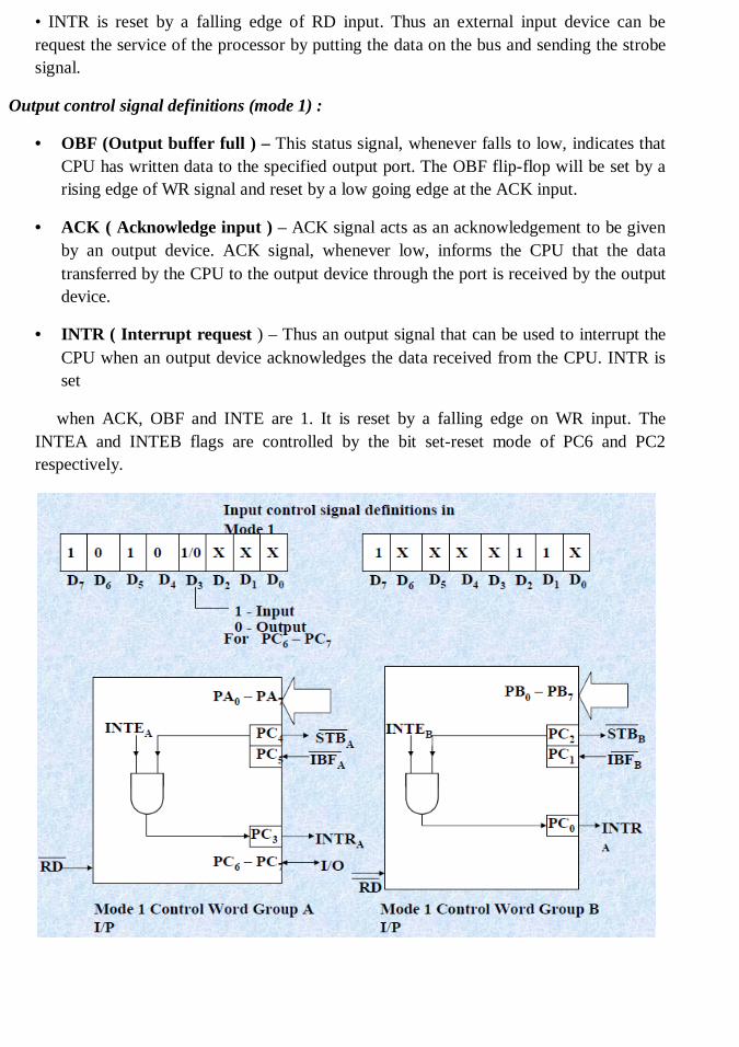
a) Mode 1: ( Strobed input/output mode ) • In this mode the handshaking signals control the input and output action of the specified
port. • Port C lines PC0-PC2, provide strobe or handshake lines for port B. This group which
includes port B and PC0-PC2 is called as group B for Strobed data input/output. • Port C lines PC3-PC5 provide strobe lines for port A. This group including port A and
PC3-PC5 from group A. Thus port C is utilized for generating handshake signals. • The salient features of mode 1 are listed as follows:
1.Two groups – group A and group B are available for strobed data transfer.
2. Each group contains one 8-bit data I/O port and one 4-bit control/data port.
3. The 8-bit data port can be either used as input and output port. The inputs and outputs both are latched.
4. Out of 8-bit port C, PC0-PC2 are used to generate control signals for port B and PC3-PC5 are used to generate control signals for port A. the lines PC6, PC7 may be used as independent data lines.
The control signals for both the groups in input and output modes are explained as follows:
Input control signal definitions (mode 1 ):
• STB( Strobe input ) – If this lines falls to logic low level,the data available at 8-bit input port is loaded into input latches.
• IBF ( Input buffer full ) – If this signal rises to logic 1, it indicates that data has been loaded into latches, i.e. It works as an acknowledgement. IBF is set by a low on STB and is reset by the rising edge of RD input.
• INTR ( Interrupt request ) – This active high output signal can be used to interrupt the CPU whenever an input device requests the service. INTR is set by a high STB pin and a high at IBF pin. INTE is an internal flag that can be controlled by the bit set/reset mode of either PC4(INTEA) or PC2(INTEB) as shown in fig.
TIST CS 305 MICROPROCESSOR AND MICROCONTROLLERS MODULE IV
Department of CSE Page 33
• INTR is reset by a falling edge of RD input. Thus an external input device can be request the service of the processor by putting the data on the bus and sending the strobe signal.
Output control signal definitions (mode 1) :
• OBF (Output buffer full ) – This status signal, whenever falls to low, indicates that CPU has written data to the specified output port. The OBF flip-flop will be set by a rising edge of WR signal and reset by a low going edge at the ACK input.
• ACK ( Acknowledge input ) – ACK signal acts as an acknowledgement to be given by an output device. ACK signal, whenever low, informs the CPU that the data transferred by the CPU to the output device through the port is received by the output device.
• INTR ( Interrupt request ) – Thus an output signal that can be used to interrupt the CPU when an output device acknowledges the data received from the CPU. INTR is set
when ACK, OBF and INTE are 1. It is reset by a falling edge on WR input. The INTEA and INTEB flags are controlled by the bit set-reset mode of PC6 and PC2 respectively.

TIST CS 305 MICROPROCESSOR AND MICROCONTROLLERS MODULE IV
Department of CSE Page 34
Mode 2 (Strobed bidirectional I/O):
Q.Specify the significance of strobed bidirectional I/O modes of 8255?
• This mode of operation of 8255 is also called as strobed bidirectional I/O. This mode
of operation provides 8255 with an additional features for communicating with a peripheral device on an 8-bit data bus. Handshaking signals are provided to maintain proper data flow and synchronization between the data transmitter and receiver. The interrupt generation and other functions are similar to mode 1.
• • In this mode, 8255 is a bidirectional 8-bit port with handshake signals. The Rd and WR
signals decide whether the 8255 is going to operate as an input port or output port. • The Salient features of Mode 2 of 8255 are listed as follows:
1. The single 8-bit port in group A is available. 2. The 8-bit port is bidirectional and additionally a 5-bit control port is available. 3. Three I/O lines are available at port C.(PC2 – PC0) 4. Inputs and outputs are both latched.

TIST CS 305 MICROPROCESSOR AND MICROCONTROLLERS MODULE IV
Department of CSE Page 35
5. The 5-bit control port C (PC3-PC7) is used for generating / accepting handshake signals for the 8-bit data transfer on port A.
Control signal definitions in mode 2: • INTR – (Interrupt request) As in mode 1, this control signal is active high and is used to
interrupt the microprocessor to ask for transfer of the next data byte to/from it. This signal is used for input (read) as well as output (write) operations.
• Control Signals for Output operations: • OBF (Output buffer full) – This signal, when falls to low level, indicates that the CPU
has written data to port A.
• ACK (Acknowledge) This control input, when falls to logic low level, acknowledges that the previous data byte is received by the destination and next byte may be sent by the processor. This signal enables the internal tristate buffers to send the next data byte on port A.
• INTE1 (A flag associated with OBF) This can be controlled by bit set/reset mode with PC6.
Control signals for input operations : • STB (Strobe input) A low on this line is used to strobe in the data into the input latches
of 8255. • IBF (Input buffer full) When the data is loaded into input buffer, this signal rises to
logic ‘1’. This can be used as an acknowledge that the data has been received by the receiver.
• Note: WR must occur before ACK and STB must be activated before RD
• The following fig shows a schematic diagram containing an 8-bit bidirectional port,
5-bit control port and the relation of INTR with the control pins. Port B can either be set to Mode 0 or 1 with port A(Group A) is in Mode 2.
• Mode 2 is not available for port B..

TIST CS 305 MICROPROCESSOR AND MICROCONTROLLERS MODULE IV
Department of CSE Page 36
• The following fig shows the control word
• The INTR goes high only if either IBF, INTE2, STB and RD go high or OBF, INTE1,
ACK and WR go high. The port C can be read to know the status of the peripheral device, in terms of the control signals, using the normal I/O
.

TIST CS 305 MICROPROCESSOR AND MICROCONTROLLERS MODULE IV
Department of CSE Page 37
The KEYBOARD/DISPLAY CONTROLLER-8279
Q.Explain the important features of KEYBOARD/DISPLAY CONTROLLER-8279
While studying 8255, we have explained the use of 8255 in interfacing keyboards and displays with 8086. The disadvantages of this method of interfacing keyboard and display with 8086 is that the processor has to refresh the display and check the status of the keyboard periodically using polling technique. Thus a considerable amount of CPU time is wasted, reducing the system operating speed.
• Intel’s 8279 is a general purpose keyboard display controller that simultaneously drives the display of a system and interfaces a keyboard with the CPU, leaving it free for its routine task.
Important features of 8279 are:-
• Simultaneous keyboard and display operations. • Scanned keyboard mode. • Scanned sensor mode. • 8 -character keyboard FIFO. • 1 6 - character display. • Right or left entry 16- byte display RAM. • Programmable scan timing •
Q.Draw the architecture of 8279?
Q.Describe Four different sections in the architecture of 8279?
Architecture and Signal Descriptions of 8279
The keyboard display controller chip 8279 provides:
a) a set of four scan lines and eight return lines for interfacing keyboards
b) A set of eight output lines for interfacing display.
Fig shows the functional block diagram of 8279 followed by its brief description.
The four major sections of 8279, they are
1)keyboard
2)scan
3)display and

TIST CS 305 MICROPROCESSOR AND MICROCONTROLLERS MODULE IV
Department of CSE Page 38
4)CPU interface
1)The keyboard section consists of
– eight return lines RL0 - RL7 that can be used to form the columns of a keyboard matrix.
• Return Buffers and Keyboard Debounce and Control: This section scans for a key closure row wise. If a key closer is detected, the keyboard debounce unit debounces the key entry (i.e. wait for 10 ms). After the debounce period, if the key continues to be detected. The code of key is directly transferred to the sensor RAM along with SHIFT and CONTROL key status.
– It has two additional input : shift and control/strobe. The keys are automatically debounced.
– The two operating modes of keyboard section are 2-key lockout and N-key rollover.
– In the 2-key lockout mode, if two keys are pressed simultaneously, only the first key is recognized.
– In the N-key rollover mode simultaneous keys are recognized and their codes are stored in FIFO.
• FIFO/Sensor RAM and Status Logic: In keyboard or strobed input mode, this block acts as 8-byte first-in-first-out (FIFO) RAM. Each key code of the pressed key is entered in the order of the entry and in the mean time read by the CPU, till the RAM become empty.
– The status logic generates an interrupt after each FIFO read operation till the FIFO is empty.
2) The display section has
• eight output lines divided into two groups A0-A3 and B0-B3.:-
– The output lines can be used either as a single group of eight lines or as two groups of four lines, in conjunction with the scan lines for a multiplexed display.
– The output lines are connected to the anodes through driver transistor in case of common cathode 7-segment LEDs.
– The cathodes are connected to scan lines through driver transistors.
– The display can be blanked by BD (low) line
• Display Address Registers and Display RAM:-

TIST CS 305 MICROPROCESSOR AND MICROCONTROLLERS MODULE IV
Department of CSE Page 39
– The display address register holds the address of the word currently being written or read by the CPU to or from the display RAM. The contents of the registers are automatically updated by 8279 to accept the next data entry by CPU.
3) The scan section has
– a scan counter:- The scan counter has two modes to scan the key matrix and refresh the display. In the encoded mode, the counter provides binary count that is to be externally decoded to provide the scan lines for keyboard and display (Four externally decoded scan lines may drive upto 16 displays). In the decode scan mode, the counter internally decodes the least significant 2 bits and provides a decoded 1 out of 4 scan on SL0-SL3(Four internally decoded scan lines may drive upto 4 displays). The keyboard and display both are in the same mode at a time.
– four scan lines, SL0 to SL3.
4)CPU interface section
• The CPU interface section takes care of data transfer between 8279 and the processor.
• This section consists of I/O Control and Data Buffers :-
– The I/O control section controls the flow of data to/from the 8279. The data buffers interface the external bus of the system with internal bus of 8279.
– The I/O section is enabled only if CS is low. The pins A0, RD and WR select the command, status or data read/write operations carried out by the CPU with 8279.
• Control and Timing Register and Timing Control : These registers store the keyboard and display modes and other operating conditions programmed by CPU. The registers are written with A0=1 and WR=0. The Timing and control unit controls the basic timings for the operation of the circuit. Scan counter divide down the operating frequency of 8279 to derive scan keyboard and scan display frequencies.
–

TIST CS 305 MICROPROCESSOR AND MICROCONTROLLERS MODULE IV
Department of CSE Page 40
Q.Explain the signal descriptions of 8279?
Q.Explain the use of BD and shift signals of 8279?

TIST CS 305 MICROPROCESSOR AND MICROCONTROLLERS MODULE IV
Department of CSE Page 41
Signal description of 8279
Fig:Logic diagram
TIST CS 305 MICROPROCESSOR AND MICROCONTROLLERS MODULE IV
Department of CSE Page 42
The signal discription of each of the pins of 8279 as follows :
• DB0-DB7 : These are bidirectional data bus lines. The data and command words to and from the CPU are transferred on these lines.
• CLK : This is a clock input used to generate internal timing required by 8279.
• RESET : This pin is used to reset 8279. A high on this line reset 8279. After resetting 8279, its in sixteen 8-bit display, left entry encoded scan, 2-key lock out mode. The clock prescaler is set to 31.
• CS : Chip Select – A low on this line enables 8279 for normal read or write operations. Other wise, this pin should remain high.
• A0 : A high on this line indicates the transfer of a command or status information. A low on this line indicates the transfer of data. This is used to select one of the internal registers of 8279.
• RD, WR (Input/Output) READ/WRITE – These input pins enable the data buffers to receive or send data over the data bus.
• IRQ : This interrupt output lines goes high when there is a data in the FIFO sensor RAM. The interrupt lines goes low with each FIFO RAM read operation but if the FIFO RAM further contains any key-code entry to be read by the CPU, this pin again goes high to generate an interrupt to the CPU.
• Vss, Vcc : These are the ground and power supply lines for the circuit.
• SL0-SL3-Scan Lines : These lines are used to scan the key board matrix and display digits. These lines can be programmed as encoded or decoded, using the mode control register.
RL0 - RL7 - Return Lines : These are the input lines which are connected to one terminal of keys, while the other terminal of the keys are connected to the decoded scan lines. These are normally high, but pulled low when a key is pressed.
• SHIFT : The status of the shift input lines is stored along with each key code in FIFO, in scanned keyboard mode. It is pulled up internally to keep it high, till it is pulled low with a key closure.
• BD – Blank Display : This output pin is used to blank the display during digit switching or by a blanking closure.
• OUT A0 – OUT A3 and OUT B0 – OUT B3 – These are the output ports for two 16*4 or 16*8 internal display refresh registers. The data from these lines is synchronized with the scan lines to scan the display and keyboard. The two 4-bit ports may also as one 8-bit port.

TIST CS 305 MICROPROCESSOR AND MICROCONTROLLERS MODULE IV
Department of CSE Page 43
• CNTL/STB- CONTROL/STROBED I/P Mode : In keyboard mode, this lines is used as a control input and stored in FIFO on a key closure. The line is a strobed lines that enters the data into FIFO RAM, in strobed input mode. It has an interrupt pull up. The lines is pulled down with a key closer.
Modes of Operation of 8279
Q.Illustrate different modes of operations of 8279?
Q.Describe different modes of operations of 8279?
Q.Differentiate input and output modes of 8279?
• The modes of operation of 8279 are as follows :
1. Input (Keyboard) modes.
2. Output (Display) modes.
1. Input (Keyboard) Modes : 8279 provides three input modes. These modes are as follows:
1. Scanned Keyboard Mode : This mode allows a key matrix to be interfaced using either encoded or decoded scans. In encoded scan, an 8*8 keyboard or in decoded scan, a 4*8 keyboard can be interfaced. The code of key pressed with SHIFT and CONTROL status is stored into the FIFO RAM.
2. Scanned Sensor Matrix : In this mode, a sensor array can be interfaced with 8279 using either encoded or decoded scans. With encoded scan 8*8 sensor matrix or with decoded scan 4*8 sensor matrix can be interfaced. The sensor codes are stored in the CPU addressable sensor RAM.
3. Strobed input: In this mode, if the control lines goes low, the data on return lines, is stored in the FIFO byte by byte.
2. Output (Display) Modes : 8279 provides two output modes for selecting the display options. These are discussed briefly.
1. Display Scan : In this mode 8279 provides 8 or 16 character multiplexed displays those can be organized as dual 4- bit or single 8-bit display units.
2. Display Entry : (right entry or left entry mode) 8279 allows options for data entry on the displays. The display data is entered for display either from the right side or from the left side.

TIST CS 305 MICROPROCESSOR AND MICROCONTROLLERS MODULE IV
Department of CSE Page 44
Keyboard Modes
i. Scanned Keyboard mode with 2 Key Lockout : In this mode of operation, when a key is pressed, a debounce logic comes into operation. During the next two scans, other keys are checked for closure and if no other key is pressed the first pressed key is identified.
The key code of the identified key is entered into the FIFO with SHIFT and CNTL status, provided the FIFO is not full, i.e. it has at least one byte free. If the FIFO does not have any free byte, naturally the key data will not be entered and the error flag is set.
• If FIFO has at least one byte free, the above code is entered into it and the 8279 generates an interrupt on IRQ line to the CPU to inform about the previous key closures. If another key is found closed during the first key, the keycode is entered in FIFO.
• If the first pressed key is released before the others, the first will be ignored. A key code is entered to FIFO only once for each valid depression, independent of other keys pressed along with it, or released before it.
• If two keys are pressed within a debounce cycle (simultaneously), no key is recognized till one of them remains closed and the other is released. The last key, that remains depressed is considered as single valid key depression.
ii. Scanned Keyboard with N-Key Rollover : In this mode, each key depression is treated independently. When a key is pressed, the debounce circuit waits for 2 keyboards scans and then checks whether the key is still depressed. If it is still depressed, the code is entered in FIFO RAM. Any number of keys can be pressed simultaneously and recognized in the order, the keyboard scan recorded them. All the codes of such keys are entered into FIFO.
In this mode, the first pressed key need not be released before the second is pressed. All the keys are sensed in the order of their depression, rather in the order the keyboard scan senses them, and independent of the order of their release.
iii. Scanned Keyboard Special Error Mode : This mode is valid only under the N-Key rollover mode. This mode is programmed using end interrupt / error mode set command. If during a single debounce period (two keyboard scans) two keys are found pressed , this is considered a simultaneous depression and an error flag is set.
• This flag, if set, prevents further writing in FIFO but allows the generation of further interrupts to the CPU for FIFO read. The error flag can be read by reading the FIFO status word. The error Flag is set by sending normal clear command with CF = 1.
iv. Sensor Matrix Mode : In the sensor matrix mode, the debounce logic is inhibited. The 8-byte FIFO RAM now acts as 8 * 8 bit memory matrix. The status of the sensor switch matrix

TIST CS 305 MICROPROCESSOR AND MICROCONTROLLERS MODULE IV
Department of CSE Page 45
is fed directly to sensor RAM matrix. Thus the sensor RAM bits contains the row-wise and column wise status of the sensors in the sensor matrix.
• The IRQ line goes high, if any change in sensor value is detected at the end of a sensor matrix scan or the sensor RAM has a previous entry to be read by the CPU. The IRQ line is reset by the first data read operation, if AI = 0, otherwise, by issuing the end interrupt command. AI is a bit in read sensor RAM word.
Display Modes
There are various options of data display. For example, the command number of characters can be 8 or 16, with each character organised as single 8-bit or dual 4-bit codes. Similarly there are two display formats.
• The first one is known as left entry mode or type writer mode, since in a type writer the first character typed appears at the left-most position, while the subsequent characters appear successively to the right of the first one. The other display format is known as right entry mode, or calculator mode, since in a calculator the first character entered appears at the rightmost position and this character is shifted one position left when the next characters is entered.
• Thus all the previously entered characters are shifted left by one position when a new characters is entered.
i. Left Entry Mode : In the left entry mode, the data is entered from left side of the display unit. Address 0 of the display RAM contains the leftmost display characters and address 15 of the RAM contains the right most display characters. It is just like writing in our address is automatically updated with successive reads or writes. The first entry is displayed on the leftmost display and the sixteenth entry on the rightmost display. The seventeenth entry is again displayed at the leftmost display position.
ii. Right Entry Mode : In this right entry mode, the first entry to be displayed is entered on the rightmost display. The next entry is also placed in the right most display but after the previous display is shifted left by one display position. The leftmost characters is shifted out of that display at the seventeenth entry and is lost, i.e. it is pushed out of the display RAM.

TIST CS 305 MICROPROCESSOR AND MICROCONTROLLERS MODULE IV
Department of CSE Page 46
DMA Controller 8257
Q.Describe the use of DMA controller?
The Direct Memory Access or DMA mode of data transfer is the fastest amongst all the modes of data transfer. In this mode, the device may transfer data directly to/from memory without any interference from the CPU. The device requests the CPU (through a DMA controller) to hold its data, address and control bus, so that the device may transfer data directly to/from memory.
The DMA data transfer is initiated only after receiving HLDA signal from the CPU. Intel’s 8257 is a four channel DMA controller designed to be interfaced with their family of microprocessors. The 8257, on behalf of the devices, requests the CPU for bus access using local bus request input i.e. HOLD in minimum mode.
In maximum mode of the microprocessor RQ/GT pin is used as bus request input. On receiving the HLDA signal (in minimum mode) or RQ/GT signal (in maximum mode) from the CPU, the requesting devices gets the access of the bus, and it completes the required number of DMA cycles for the data transfer and then hands over the control of the bus back to the CPU.
Internal Architecture of 8257
Q.Describe the internal architecture of 8257?
Q.Describe the important features of 8257?

TIST CS 305 MICROPROCESSOR AND MICROCONTROLLERS MODULE IV
Department of CSE Page 47
The internal architecture of 8257 is shown in figure. The chip support four DMA channels, i.e. four peripheral devices can independently request for DMA data transfer through these channels at a time. The DMA controller has 8-bit internal data buffer, a read/write unit, a control unit, a priority resolving unit along with a set of registers.
Features:
It is a 4-channel DMA. So 4 I/O devices can be interfaced to DMA It is designed by Intel Each channel have 16-bit address and 14 bit counter It provides chip priority resolver that resolves priority of channels in fixed or
rotating mode.
It provide on chip channel inhibit logic.
Register Organization of 8257
Q.Explain the register organization of 8257
Q.Explain the use of terminal count register in 8257?

TIST CS 305 MICROPROCESSOR AND MICROCONTROLLERS MODULE IV
Department of CSE Page 48
Each channel has a pair of 2 16 bit registers:- DMA address register Terminal Count register
Two common registers for all channels are:- Mode set register Status register
So total 10 registers,they are selected using A0-A3 address lines
DMA Address Register
Each DMA channel has one DMA address register. The function of this register is to store the address of the starting memory location, which will be accessed by the DMA channel. Thus the starting address of the memory block which will be accessed by the device is first loaded in the DMA address register of the channel. The device that wants to transfer data over a DMA channel, will access the block of the memory with the starting address stored in the DMA Address Register.
Terminal Count Register
Each of the four DMA channels of 8257 has one terminal count register (TC). This 16-bit register isused for ascertaining that the data transfer through a DMA channel ceases or stops after the required number of DMA cycles. The low order 14-bits of the terminal

TIST CS 305 MICROPROCESSOR AND MICROCONTROLLERS MODULE IV
Department of CSE Page 49
count register are initialised with the binary equivalent of the number of required DMA cycles minus one.After each DMA cycle, the terminal count register content will be decremented by one and finally it becomes zero after the required number of DMA cycles are over. The bits 14 and 15 of this register indicate the type of the DMA operation (transfer). If the device wants to write data into the memory, the DMA operation is called DMA write operation. Bit 14 of the register in this case will be set to one and bit 15 will be set to zero. Table gives detail of DMA operation selection and corresponding bit configuration of bits14 and 15 of the TC register.
Mode Set Register
Q.Explain the modes of operations of 8257( Explain the mode set register )
Q.Draw the control word format of mode set register and status register?
The mode set register is used for programming the 8257 as per the requirements of the system. The function of the mode set register is to enable the DMA channels individually and also to set the various modes of operation.The DMA channel should not be enabled till the DMA address register and the terminal count register contain valid information, otherwise, an unwanted DMA request may initiate a DMA cycle, probably destroying the valid memory data. The bits Do-D3 enable one of the four DMA channels of 8257. for example, if Do is ‘1’, channel 0 is enabled. If bit 4 is set, rotating priority is enabled, otherwise, the normal, i.e. fixed priority is enabled.
TIST CS 305 MICROPROCESSOR AND MICROCONTROLLERS MODULE IV
Department of CSE Page 50
If the TC STOP bit is set, the selected channel is disabled after the terminal count condition is reached, and it further prevents any DMA cycle on the channel. To enable the channel again, this bit must be reprogrammed. If the TC STOP bit is programmed to be zero, the channel is not disabled, even after the count reaches zero and further request are allowed on the same channel. The auto load bit, if set, enables channel 2 for the repeat block chaining operations, without immediate software intervention between the two successive blocks. The channel 2 registers are used as usual, while the channel 3 registers are used to store the block reinitialisation parameters, i.e. the DMA starting address and terminal count. After the first block is transferred using DMA, the channel 2 registers are reloaded with the corresponding channel 3 registers for the next block transfer, if the update flag is set.
The extended write bit, if set to ‘1’, extends the duration of MEMW and IOW signals by activating them earlier, this is useful in interfacing the peripherals with different access times. If the peripheral is not accessed within the stipulated time, it is expected to give the ‘NOT READY’ indication to 8257, to request it to add one or more wait states in the DMA CYCLE. The mode set register can only be written into.
Status Register
The status register of 8257 is shown in figure. The lower order 4-bits of this register contain the terminal count status for the four individual channels. If any of these bits is set, it indicates that the specific channel has reached the terminal count condition.
These bits remain set till either the status is read by the CPU or the 8257 is reset. The update flag is not affected by the read operation. This flag can only be cleared by resetting 8257 or by resetting the auto load bit of the mode set register. If the update flag is set, the contents of the channel 3 registers are reloaded to the corresponding registers of channel 2 whenever the channel 2 reaches a terminal count condition, after transferring one block and the next block is to be transferred using the autoload feature of 8257. The update flag is set every time, the channel 2 registers are loaded with contents of the channel 3 registers. It is cleared by the completion of the first DMA cycle of the new block. This register can only read.
Data Bus Buffer, Read/Write Logic, Control Unit and Priority Resolver

TIST CS 305 MICROPROCESSOR AND MICROCONTROLLERS MODULE IV
Department of CSE Page 51
Q.Describe the duty of priority resolver in 8257?
The 8-bit. Tristate, bidirectional buffer interfaces the internal bus of 8257 with the external system bus under the control of various control signals.
In the slave mode, the read/write logic accepts the I/O Read or I/O Write signals, decodes the Ao-A3 lines and either writes the contents of the data bus to the addressed internal register or reads the contents of the selected register depending upon whether IOW or IOR signal is activated.
In master mode, the read/write logic generates the IOR and IOW signals to control the data flow to or from the selected peripheral.
The control logic controls the sequences of operations and generates the required control signals like AEN, ADSTB, MEMR,MEMW, TC and MARK along with the address lines A4-A7, in master mode.
The priority resolver resolves the priority of the four DMA channels depending upon whether normal priority or rotating priority is programmed.
Signal Description of 8257
Q.Draw the pin configuration of 8257?
Q.Draw the signal diagram of 8257?
Q.Describe the following pins of 8257 :- a)HRQ b)ADST C)Mark d)TC
DRQo-DRQ3 :
These are the four individual channel DMA request inputs, used by the peripheral devices for requesting the DMA services. The DRQo has the highest priority while DRQ3 has the lowest one, if the fixed priority mode is selected.
DACKo-DACK3 :

TIST CS 305 MICROPROCESSOR AND MICROCONTROLLERS MODULE IV
Department of CSE Page 52
These are the active-low DMA acknowledge output lines which inform the requesting peripheral that the request has been honoured and the bus is relinquished by the CPU. These lines may act as strobe lines for the requesting devices.
Do-D7:
These are bidirectional, data lines used to interface the system bus with the internal data bus of 8257. These lines carry command words to 8257 and status word from 8257, in slave mode, i.e. under the control of CPU. The data over these lines may be transferred in both the directions. When the 8257 is the bus master (master mode, i.e. not under CPU control), it uses Do-D7 lines to send higher byte of the generated address to the latch. This address is further latched using ADSTB signal. the address is transferred over Do-D7 during the first clock cycle of the DMA cycle. During the rest of the period, data is available on the data bus.
IOR:
This is an active-low bidirectional tristate input line that acts as an input in the slave mode. In slave mode, this input signal is used by the CPU to read internal registers of 8257.this line acts output in master mode. In master mode, this signal is used to read data from a peripheral during a memory write cycle.
IOW :
This is an active low bidirection tristate line that acts as input in slave mode to load the contents of the data bus to the 8-bit mode register or upper/lower byte of a 16-bit DMA
TIST CS 305 MICROPROCESSOR AND MICROCONTROLLERS MODULE IV
Department of CSE Page 53
address register or terminal count register. In the master mode, it is a control output that loads the data to a peripheral during DMA memory read cycle (write to peripheral).
CLK:
This is a clock frequency input required to derive basic system timings for the internal operation of 8257.
RESET :
This active-high asynchronous input disables all the DMA channels by clearing the mode register and tristates all the control lines.
Ao-A3:
These are the four least significant address lines. In slave mode, they act as input which select one of the registers to be read or written. In the master mode, they are the four least significant memory address output lines generated by 8257.
CS:
This is an active-low chip select line that enables the read/write operations from/to 8257, in slave mode. In the master mode, it is automatically disabled to prevent the chip from getting selected (by CPU) while performing the DMA operation.
A4-A7 :
This is the higher nibble of the lower byte address generated by 8257 during the master mode of DMA operation.
READY:
This is an active-high asynchronous input used to stretch memory read and write cycles of 8257 by inserting wait states. This is used while interfacing slower peripherals..
HRQ:
The hold request output requests the access of the system bus. In the noncascaded 8257 systems, this is connected with HOLD pin of CPU. In the cascade mode, this pin of a slave is connected with a DRQ input line of the master 8257, while that of the master is connected with HOLD input of the CPU.
HLDA :The CPU drives this input to the DMA controller high, while granting the bus to the device. This pin is connected to the HLDA output of the CPU. This input, if high, indicates to the DMA controller that the bus has been granted to the requesting peripheral by the CPU.

TIST CS 305 MICROPROCESSOR AND MICROCONTROLLERS MODULE IV
Department of CSE Page 54
MEMR:
This active –low memory read output is used to read data from the addressed memory locations during DMA read cycles.
MEMW :
This active-low three state output is used to write data to the addressed memory location during DMA write operation.
ADST :
This output from 8257 strobes the higher byte of the memory address generated by the DMA controller into the latches.
AEN:
This output is used to disable the system data bus and the control the bus driven by the CPU, this may be used to disable the system address and data bus by using the enable input of the bus drivers to inhibit the non-DMA devices from responding during DMA operations. If the 8257 is I/O mapped, this should be used to disable the other I/O devices, when the DMA controller addresses is on the address bus.
TC:
Terminal count output indicates to the currently selected peripherals that the present DMA cycle is the last for the previously programmed data block. If the TC STOP bit in the mode set register is set, the selected channel will be disabled at the end of the DMA cycle. The TC pin is activated when the 14-bit content of the terminal count register of the selected channel becomes equal to zero. The lower order 14 bits of the terminal count register are to be programmed with a 14-bit equivalent of (n-1), if n is the desired number of DMA cycles.
MARK :
The modulo 128 mark output indicates to the selected peripheral that the current DMA cycle is the 128th cycle since the previous MARK output. The mark will be activated after each 128 cycles or integral multiples of it from the beginning if the data block (the first DMA cycle), if the total number of the required DMA cycles (n) is completely divisible by 128.
Vcc :This is a +5v supply pin required for operation of the circuit.
GND :
This is a return line for the supply (ground pin of the IC).


![Full page photo - Mahavir Swami Institute of Technology · ET'E( '-305 Microprocessor & M lcrocontl ollers ETF,L-3()5 Signals & stems Sensors & Transducers li]WC-405 Wireless ETF.L](https://img.dokumen.tips/doc/110x75/6072f6dba53c9b51013a74fc/full-page-photo-mahavir-swami-institute-of-ete-305-microprocessor-m.jpg)