Embed Size (px)
Citation preview

CSNB374: Microprocessor Systems
Chapter 2: Intel x86 Microprocessor Architecture

Introduction Most Intel microprocessors uses an
instruction set called x86 (IA-32). A CISC instruction set. Always being extended by Intel when they
develop a new microprocessor. The 64-bit extension of this instruction
set is called x86-64. Supports larger virtual and physical address
space. Backward compatible with x86. Implemented in the later versions of
Pentium 4 and above.

History of Intel Microprocessors
Intel 4004 The world’s first microprocessor Introduced in 1971 4-bit microprocessor Can only support 4K of memory
Each address location contains only 4-bit (1 nibble) of data
Instruction set contains 45 instructions

History of Intel Microprocessors Intel 8008
8-bit version of Intel 4004 microprocessor Supports 16K of memory
Each memory location can store 8-bit (1 byte) of data
Introduced in 1972 Instruction set contains 48 instructions Small memory size, slow speed and
limited instruction set limits the 8008 usefulness

History of Intel Microprocessors Intel 8080
The first of the modern 8-bit microprocessors
Introduced in 1974 Supports 64K of memory 10 times faster than Intel 8008 Compatible with TTL (transistor to
transistor logic) Allows for easier interfacing

History of Intel Microprocessors Intel 8085
An updated version of Intel 8080 Introduced in 1977 The last 8-bit microprocessor from Intel Advantages compared to Intel 8080:
Higher clock frequency Internal clock generator and system controller
The higher level of component integration allows simpler and less expensive microcomputers to be built
Instruction set contains 246 instructions

History of Intel Microprocessors Intel 8086 and 8088
Intel 8086 is the first microprocessor using the x86 instruction set
Intel 8086 was introduced in 1978 while Intel 8088 was introduced in 1979
Both are 16-bit microprocessors Supports 1MB (1024 K) of memory
Both processors have the same architecture except for the external data bus width
Intel 8086 has 16-bit external data bus Intel 8088 has 8-bit external data bus

History of Intel Microprocessors
The use of 8-bit external data bus allows Intel 8088 to be compatible with 8-bit support chips (which is cheaper than 16-bit support chips)
Also contains 4/6-byte instruction cache that prefetches instructions before they were executed
Speed up the operation of many sequences of instructions
Basis for much larger instruction caches found in modern microprocessors
Instruction set contains over 20,000 variations of instructions
Include multiply and divide instructions which were missing in earlier microprocessors

History of Intel Microprocessors Intel 80286
An updated version of 8086 Still a 16-bit microprocessor
Introduced in 1982 Supports 16M of memory Provides improved performance over Intel
8086: Higher clock speed Changes to internal execution of instructions
The first x86 microprocessor to provide protected mode
Allows features such as virtual memory, paging and safe multitasking (with memory protection)

History of Intel Microprocessors Intel 80386
The first 32-bit microprocessor 32-bit data bus and memory address
Introduced in 1985 Support 4GB of memory Provides memory management unit
Allows memory resources to be managed by the OS
Instruction set compatible with earlier 16-bit Intel microprocessors
Allow 16-bit software to run

History of Intel Microprocessors Intel 80486
An integrated chip which incorporates: 80386-like microprocessor 80387-like numeric coprocessor 8K-byte cache memory system
Introduced in 1989 Changes made to internal structure so
that half of its instructions are executed in one clock cycle instead of two

History of Intel Microprocessors Intel Pentium
The original Pentium is based on the P5 microarchitecture
Introduced in 1993 Provides faster clock speed and larger
cache compared 80386 and 80486 Data bus width is increased to 64 bits Later Pentium models include the
multimedia extensions (MMX)

History of Intel Microprocessors The Pentium trademark is used by Intel for
a long line of microprocessors that are based on various different microarchitectures. P6 microarchitecture: Pentium Pro, Pentium II,
Pentium III Netburst microarchitecure: Pentium 4, Pentium
D Pentium M microarchitecture: Pentium M Core microarchitecture: Pentium Dual-Core,
Pentium Nehalem microarchitecture: Pentium

History of Intel Microprocessors Intel Core2, Core i3, Core i5, Core i7
After Pentium 4, it becomes impractical to improve performance by increasing clock speed
Intel starts to put multiple cores in one chip Increase speed of multithreaded applications Provides 64-bit extension
A feature that has been there since later versions of Pentium 4
Theoretically allow for 64-bit address However, earlier Intel Core2 microprocessor contains
only 40 address pins which supports 1TB of memory Allows for 64-bit arithmetic

History of Intel Microprocessors Other Intel microprocessors
Intel Celeron: Low-end version
Intel Xeon: High-end version for servers and workstations Support multiprocessor
Intel Atom: For ultra-mobile devices
Intel Itanium: Allows greater parallelism than traditional
architecture Uses IA-64 instruction set (incompatible with x86/IA-
32) Used in high-end servers

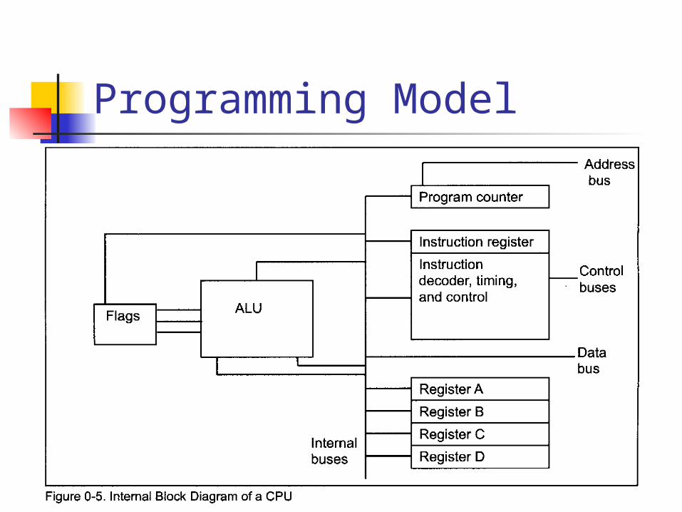
Programming Model Microprocessors can be programmed
directly using an assembly language. Differences with high-level languages:
Use commands to execute data movements, arithmetic, logic and program control operations.
Use registers to hold data for operation. Programmers need to know not only the
assembly language for the microprocessor, but also the internal configuration of the microprocessor.
Programming Model

Registers A register is a storage element inside a
microprocessor. Almost all operations would involve
using registers. Some registers are general purpose
registers, while others have special purposes. General purpose registers can hold various
data sizes and used for almost any purpose as dictated by the program.
However, each general purpose register does have its own special purposes.

Registers

RegistersSince the x86 instruction set is designed to be compatible with previous microprocessors, the same register can be accessed using different names.Different names are given for 64-bit, 32-bit, 16-bit and 8-bit version of the same register.

General Purpose Registers RAX, EAX, AX (AH & AL)
A general purpose register Also an accumulator – stores intermediate
results after arithmetic and logic operations Can also hold the offset address of a
location in memory (80386 and above) RBX, EBX, BX (BH & BL)
A general purpose register Also a base index register – holds the offset
address of a location in memory Can also address memory data (80386 and
above)

General Purpose Registers RCX, ECX, CX (CH & CL)
A general purpose register Also a count register – holds the count for
various instructions Can also hold the offset address of a location
in memory (80386 and above) RDX, EDX, DX (DH & DL)
A general purpose register Also a data register – stores data related to
accumulator’s calculation (multiply and divide) Can also address memory data (80386 and
above)

General Purpose Registers RBP, EBP, BP
A general purpose register Also a base pointer register – points to a
memory location for memory data transfer
RDI, EDI, DI A general purpose register Also a destination index register – holds
the memory address for the destination data of a string instruction

General Purpose Registers RSI, ESI, SI
A general purpose register Also a source index register - holds the
memory address for the source data of a string instruction
R8 through R15 General purpose registers Found only in 64-bit microprocessors Data are addressed in 64-, 32-, 16-, or 8-bit
sizes

Special Purpose Registers RIP, EIP, IP
Instruction pointer – points to the next instruction in the memory to be executed
RSP, ESP, SP Stack pointer – points to an area in memory
called the stack RFLAGS, EFLAGS, FLAGS
Indicates the condition of the microprocessor and control its operation

Flags

Flags
The C, P, A, Z, S and O flags are changed by most arithmetic and logic operations.
Flags never change for any data transfer or program control operations.
Some flags are also used to control features found in the microprocessor.

Flags Descriptions for some of the flag bits:
C (carry): holds the carry after addition or borrow after subtraction.
P (parity): the count of 1s in a number expressed as even or odd.
0 for odd, 1 for even. A (auxiliary carry): holds the half-carry after
addition or the borrow after subtraction between bit positions 3 and 4 of the result.

Flags Z (zero): shows that the result of an arithmetic
or logic operation is zero. 0 result is not zero, 1 result is zero.
S (sign): holds the arithmetic sign of the result after an arithmetic or logic instruction executes.
0 for positive, 1 for negative. T (trap): enables trapping through an on-chip
debugging feature. 0 disable trapping, 1 enable trapping. If enabled, allows the microprocessor to interrupt the
flow of the program on conditions indicated by the debug registers and control registers.
Microsoft Visual Studio debugging tool uses this feature.

Flags I (interrupt): control the operation of the
INTR (interrupt request) input pin. 0 disables INTR pin, 1 enables INTR pin.
D (direction): selects increment or decrement mode for SI/DI registers. 0 increment, 1 decrement.
O (overflow): indicates that the result of an addition/subtraction of signed numbers exceeded the capacity of the machine.

Segment Registers Generate memory addresses when
combined with other registers in the microprocessor.
Function differently in real mode than in protected mode.
List of segment registers: CS (code segment): defines the memory area that
contains the code (programs and procedures) DS (data segment): defines the memory area that
contains most data used by a program.

Segment Registers ES (extra segment): defines the
memory area that contains additional data segment used by some string instructions to hold destination data.
SS (stack segment): defines the memory area that is used for the stack.
FS and GS: supplemental segment registers available in 80386 and above.

Memory Organization Memory stores addresses of instructions and
data. These value are used by the processor to access
memory locations. We begin with the memory organization.
Chap 1 explained that memory is a collection of bytes.
Each memory bytes has an address, starting with 0. The 8086 processor assigns 20-bit physical address to its memory locations. Thus it is possible to address 220 = 1, 048, 576 bytes (1MB) of memory.

The first five bytes in memory have the following addresses:
Because addresses are so cumbersome to write inbinary, we usually express them as five hex digits, -> And so on. The highest address is FFFFFh
Address Content
00000000000000000000
00000000000000000001
00000000000000000001
0000000000000000001100000000000000000100
Address Content
00000
00001
00002.
.
00009
0000A0000B
.
.

Segmented Memory
In order to explain the function of the segment registers; need to introduce the idea of memory segments, which is a direct consequence of using a 20-bit address in a 16-bit processor.
The address are too big to fit in a 16-bit register.
Solution!!-> by partitioning its memory into segments.

A mechanism that allows the extend the addressability of a Processor
It uses 2 components to specify memory locations: a segment value and an offset value within that segment.
Segmented Memory

A memory segment is a block of 216 (or 64k) consecutive memory bytes.
Each segment is identified by a segment number.
Within a segment, a memory location is specified by giving an offset.
This is the number of bytes from the beginning of the segment.
Segmented Memory

A memory location may be specified by providing a segment number and an offset, written in the form segment:offset; this is know as a logical address
In the 8086 processor each 20bit address is expressed as: 16 bit segment 16 bit offset Example: 2000h:0BAFh
Means offset 0BAFh within segment 2000h.
Segmented Memory

Real Mode Memory Addressing All Intel microprocessors before 80286
can only operate in real mode. 80286 and above can operate in both real
and protected mode. Real mode operation allows addressing
of only the first 1MB of memory space. True even in latest Intel microprocessors. The first 1MB of memory is called the real
memory, conventional memory or DOS memory.
Intel microprocessors begins operating in real mode by default.

Real Mode Memory Addressing
Generation of 20-bit linear address (physical address) from a segment:offset address
in the real mode, each segment register (16 bits) is internally appended with a 0h on its rightmost end (i.e., the segment is shifted left by 4 bits)
The segment and the offset are then added to form 20-bit memory address.

Segments and Offsets All real mode memory addresses consist of
a segment address plus an offset address. Segment address defines the beginning of any
64KB memory segment. Offset address selects any location within the
64KB memory segment. Can be written in the form segment:offset
Example: 10000:F000 Segment address = 0x10000 Offset address = 0xF000

Segments and Offsets Given a segment and an offset address,
the actual linear address (physical address) is calculated as follows: Linear addr = (segment addr x 10H) + offset
addr Example 1: 1000:F000
Linear addr = (1000H x 10H) + F000H = 10000H + F000H = 1F000H
Example 2: 020A:1BCD Linear addr = (020AH x 10H) + 1BCDH
= 020A0H + 1BCDH = 03C6DH
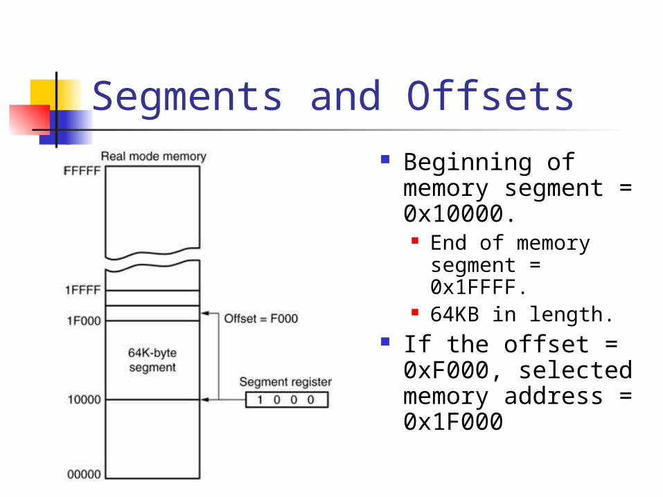
Segments and Offsets Beginning of
memory segment = 0x10000. End of memory
segment = 0x1FFFF.
64KB in length. If the offset =
0xF000, selected memory address = 0x1F000

Segments and Offsets The segment address is stored in one of
the segment registers. The offset address is stored in one of
the general purpose registers. The segment plus offset addressing
allows program or data to be relocated. The program or data segment can be placed
anywhere in the memory and executed or used without any change to the program.

Segments and Offsets
Segment
Offset Special Purpose
CS IP Instruction address
SS SP or BP Stack address
DS BX, DI, SI, an 8- or 16-bit number
Data address
ES DI for string instructions
String destination addressDefault 16-bit segment and offset combinations

Segments and Offsets: Use of Segments

Protected Mode Memory Addressing Protected mode allows access to data
and programs located within and above the first 1MB of memory. Microsoft Windows operates in protected
mode. The segment registers are used
differently in protected mode. They no longer store the segment address. Instead, they contain a selector that selects a
descriptor from a descriptor table.

Protected Mode Memory Addressing
The contents of a segment register during protected mode operation of the 80286 through Core2 microprocessors.

Protected Mode Memory Addressing A descriptor table can contain up to
8192 descriptors. There are two types of descriptor
tables: Global descriptors: contain segment
definitions that apply to all programs. Local descriptors: unique to an application.
A descriptor contains information about: Memory segment’s location Length of the segment Access rights

Protected Mode Memory Addressing

Protected Mode Memory Addressing – Example