Embed Size (px)
Citation preview
Dragomir [email protected]
ELEC-H-473Microprocessor architecture
Intel x86 micro-architectureIntro and NetBurst architecture
Lecture 09
Friday 11 April 14 (-38)
Université libre de Bruxelles/Faculté des Sciences Appliquées/BEAMS/MILOJEVIC Dragomir
Previously ...
• Some basic concepts necessary to understand in more detailed manner current CPU architectures :
✓ basic execution environment
✓ few technology issues and their impact on themicro-processor architecture
✓ need for parallelism : ❖ for high-performance multi-media computing (SIMD), ❖ but also more general parallel computing (thread-
level parallelism)
2
Friday 11 April 14 (-38)
Université libre de Bruxelles/Faculté des Sciences Appliquées/BEAMS/MILOJEVIC Dragomir
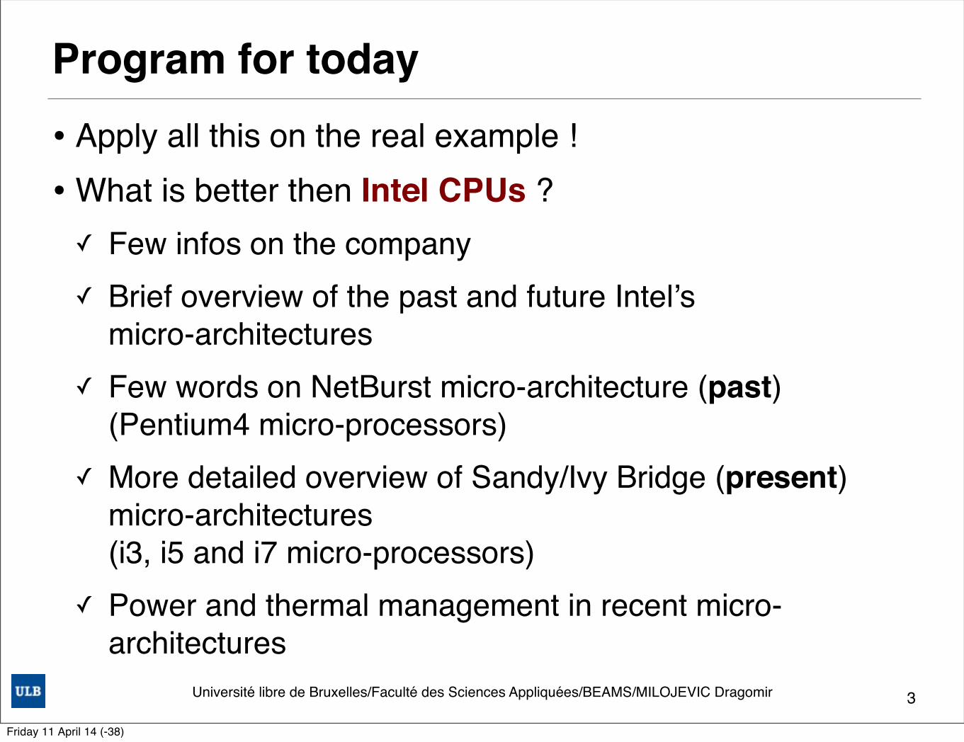
Program for today
• Apply all this on the real example !• What is better then Intel CPUs ? ✓ Few infos on the company✓ Brief overview of the past and future Intel’s
micro-architectures✓ Few words on NetBurst micro-architecture (past)
(Pentium4 micro-processors)✓ More detailed overview of Sandy/Ivy Bridge (present)
micro-architectures(i3, i5 and i7 micro-processors)
✓ Power and thermal management in recent micro-architectures
3
Friday 11 April 14 (-38)
Université libre de Bruxelles/Faculté des Sciences Appliquées/BEAMS/MILOJEVIC Dragomir
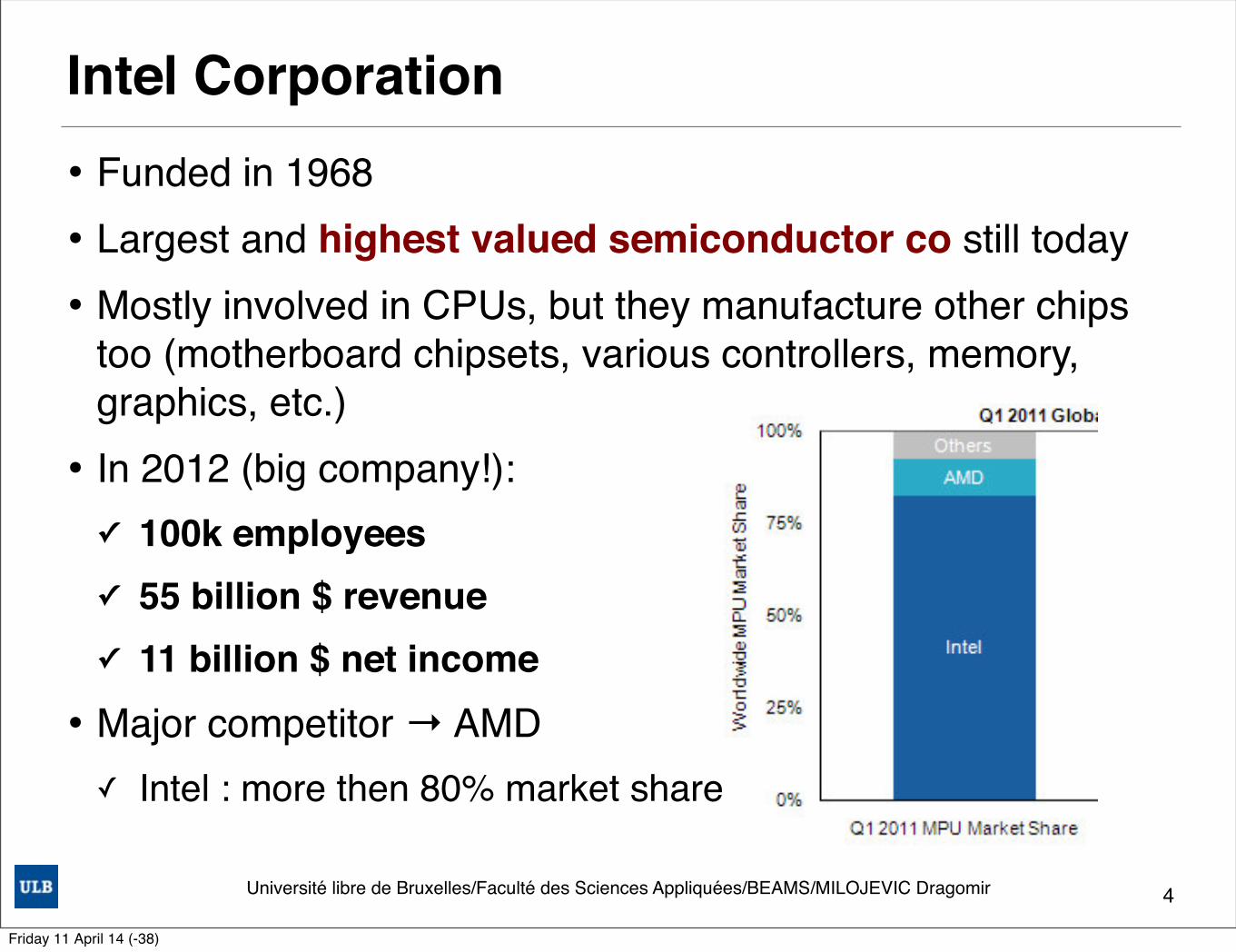
Intel Corporation• Funded in 1968 • Largest and highest valued semiconductor co still today• Mostly involved in CPUs, but they manufacture other chips
too (motherboard chipsets, various controllers, memory, graphics, etc.)
• In 2012 (big company!):✓ 100k employees ✓ 55 billion $ revenue✓ 11 billion $ net income
• Major competitor → AMD✓ Intel : more then 80% market share
4
Friday 11 April 14 (-38)
Université libre de Bruxelles/Faculté des Sciences Appliquées/BEAMS/MILOJEVIC Dragomir
Intel’s strategy from the start• Combine :✓ Technology development for (proprietary) IC manufacturing
(AKA process technology)✓ Circuit design (i.e. IC architecture)
• Keep both aspects for themselves only !!! → This was true until now : FPGAs vendors (Altera) might use their 14nm fab (revolution!)
• At some point in time Tech & Design were considered to be independent :✓ Split into : Fab + Fabless companies → Intel always ignored that with success
✓ As we move along towards more and more advanced technologies, these two become very closely coupled
✓ “Alone” approach not sustainable any more, hence the open-up
5
Friday 11 April 14 (-38)
Université libre de Bruxelles/Faculté des Sciences Appliquées/BEAMS/MILOJEVIC Dragomir
Intel’s product line• Focuses mostly on micro-processor market
• Targets mostly high-performance (and thus high-power) devices for laptops, desktops, servers, data-centers and super-computing
• In that field they have very little competition ...
• However one thing they missed is low-power applications !
• There was some trials to enter low-power market, but this ended with nothing great ✓ ARM already created significant niche in this domain and
established them as major player❖ Guess what is inside iPhone, iPad etc …
6
Friday 11 April 14 (-38)
Université libre de Bruxelles/Faculté des Sciences Appliquées/BEAMS/MILOJEVIC Dragomir
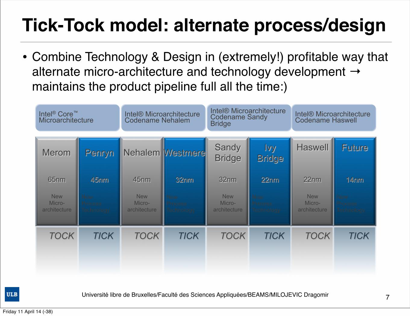
Tick-Tock model: alternate process/design
71 2/15/12
Tick-Tock Development Model: Sustained Microprocessor Leadership
Intel® Core™ Microarchitecture
TOCK
New Micro-
architecture
Merom
65nm
TICK
Penryn
New Process Technology
45nm
Intel® Microarchitecture Codename Nehalem
TOCK
New Micro-
architecture
Nehalem
45nm
TICK
Westmere
32nm
New Process Technology
Intel® Microarchitecture Codename Sandy Bridge
TOCK
Sandy Bridge
32nm
New Micro-
architecture
TICK
Ivy Bridge
22nm
New Process Technology
Intel® Microarchitecture Codename Haswell
TOCK
Haswell
22nm
New Micro-
architecture
TICK
Future
14nm
New Process Technology
• Combine Technology & Design in (extremely!) profitable way that alternate micro-architecture and technology development → maintains the product pipeline full all the time:)
Friday 11 April 14 (-38)
Université libre de Bruxelles/Faculté des Sciences Appliquées/BEAMS/MILOJEVIC Dragomir
Intel nomenclature disambiguation • Micro—architecture : key differentiator, defines ISA,
there are 2 major releases : ✓ x86 → laptop/desktop/server
depending on data/address path bit width ❖ CISC ❖ 32 bit and now 64 bit
✓ Itanium → servers/high-performance computing❖ VLIW based architecture❖ remained low-volume❖ still in the roadmap
• Micro-architecture code name✓ Each of the above will have a specific code name
(e.g. NetBurst or Nehelem)• Brand name — this what you by in the end of the day✓ Pentium 4 (NetBurst) or i7 (Nehelem)
8
Friday 11 April 14 (-38)
From 8086to planned future generations
Friday 11 April 14 (-38)
Université libre de Bruxelles/Faculté des Sciences Appliquées/BEAMS/MILOJEVIC Dragomir
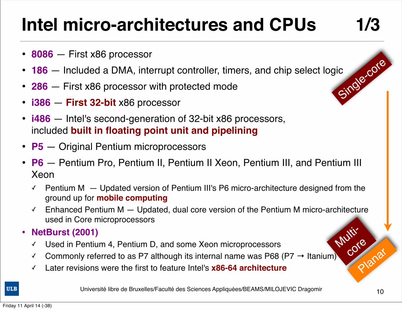
Intel micro-architectures and CPUs 1/3• 8086 — First x86 processor• 186 — Included a DMA, interrupt controller, timers, and chip select logic• 286 — First x86 processor with protected mode• i386 — First 32-bit x86 processor• i486 — Intel's second-generation of 32-bit x86 processors,
included built in floating point unit and pipelining • P5 — Original Pentium microprocessors• P6 — Pentium Pro, Pentium II, Pentium II Xeon, Pentium III, and Pentium III
Xeon ✓ Pentium M — Updated version of Pentium III's P6 micro-architecture designed from the
ground up for mobile computing✓ Enhanced Pentium M — Updated, dual core version of the Pentium M micro-architecture
used in Core microprocessors• NetBurst (2001)
✓ Used in Pentium 4, Pentium D, and some Xeon microprocessors✓ Commonly referred to as P7 although its internal name was P68 (P7 → Itanium)✓ Later revisions were the first to feature Intel's x86-64 architecture
10
Multi-
core
Single-core
Planar
Friday 11 April 14 (-38)
Université libre de Bruxelles/Faculté des Sciences Appliquées/BEAMS/MILOJEVIC Dragomir
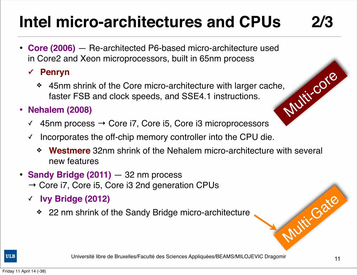
Intel micro-architectures and CPUs 2/3• Core (2006) — Re-architected P6-based micro-architecture used
in Core2 and Xeon microprocessors, built in 65nm process✓ Penryn
❖ 45nm shrink of the Core micro-architecture with larger cache, faster FSB and clock speeds, and SSE4.1 instructions.
• Nehalem (2008)✓ 45nm process → Core i7, Core i5, Core i3 microprocessors✓ Incorporates the off-chip memory controller into the CPU die.
❖ Westmere 32nm shrink of the Nehalem micro-architecture with several new features
• Sandy Bridge (2011) — 32 nm process → Core i7, Core i5, Core i3 2nd generation CPUs✓ Ivy Bridge (2012)
❖ 22 nm shrink of the Sandy Bridge micro-architecture
11
Multi-core
Multi-Gate
Friday 11 April 14 (-38)
Université libre de Bruxelles/Faculté des Sciences Appliquées/BEAMS/MILOJEVIC Dragomir
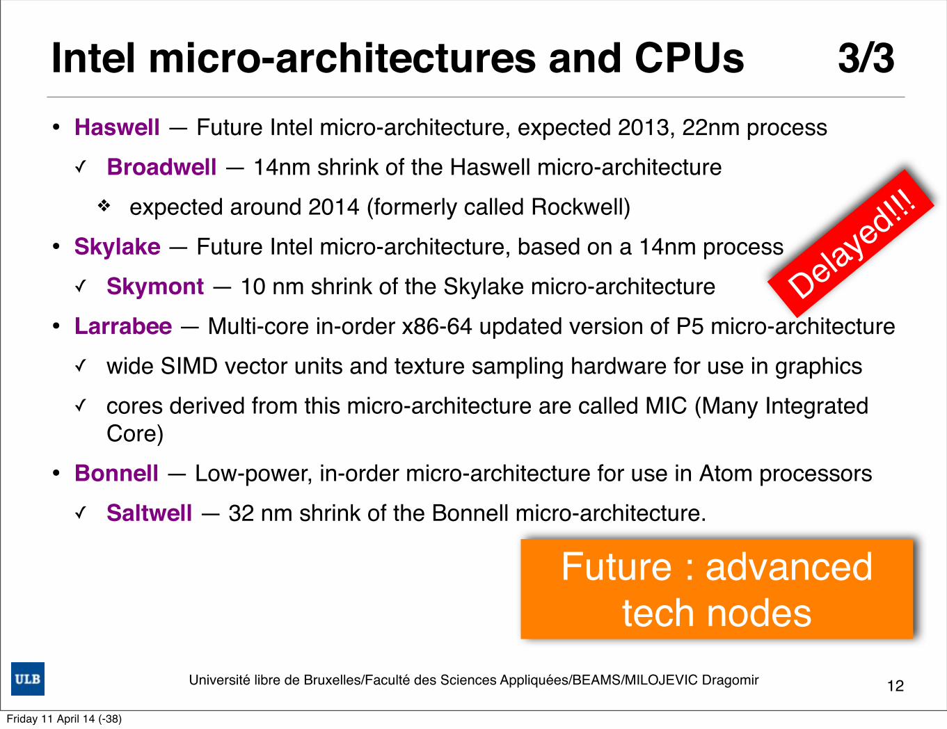
Intel micro-architectures and CPUs 3/3• Haswell — Future Intel micro-architecture, expected 2013, 22nm process✓ Broadwell — 14nm shrink of the Haswell micro-architecture
❖ expected around 2014 (formerly called Rockwell)
• Skylake — Future Intel micro-architecture, based on a 14nm process✓ Skymont — 10 nm shrink of the Skylake micro-architecture
• Larrabee — Multi-core in-order x86-64 updated version of P5 micro-architecture✓ wide SIMD vector units and texture sampling hardware for use in graphics✓ cores derived from this micro-architecture are called MIC (Many Integrated
Core)
• Bonnell — Low-power, in-order micro-architecture for use in Atom processors✓ Saltwell — 32 nm shrink of the Bonnell micro-architecture.
12
Future : advanced tech nodes
Delayed!!!
Friday 11 April 14 (-38)
Université libre de Bruxelles/Faculté des Sciences Appliquées/BEAMS/MILOJEVIC Dragomir
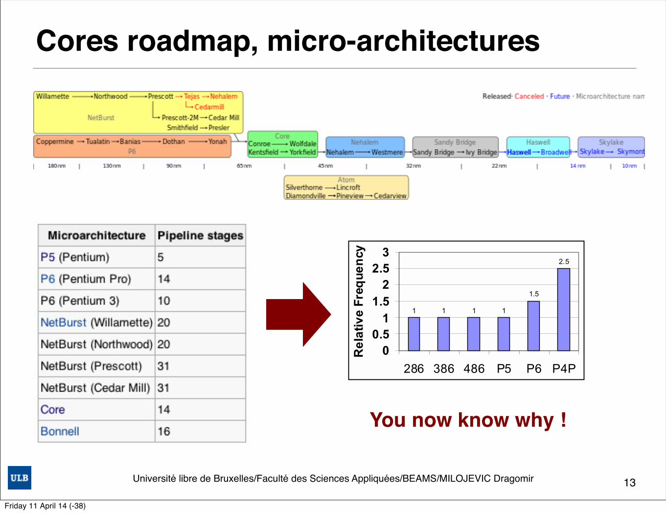
Cores roadmap, micro-architectures
13
Intel Technology Journal Q1, 2001
The Microarchitecture of the Pentium 4 Processor 3
CLOCK RATES Processor microarchitectures can be pipelined to different degrees. The degree of pipelining is a microarchitectural decision. The final frequency of a specific processor pipeline on a given silicon process technology depends heavily on how deeply the processor is pipelined. When designing a new processor, a key design decision is the target design frequency of operation. The frequency target determines how many gates of logic can be included per pipeline stage in the design. This then helps determine how many pipeline stages there are in the machine.
There are tradeoffs when designing for higher clock rates. Higher clock rates need deeper pipelines so the efficiency at the same clock rate goes down. Deeper pipelines make many things take more clock cycles, such as mispredicted branches and cache misses, but usually more than make up for the lower per-clock efficiency by allowing the design to run at a much higher clock rate. For example, a 50% increase in frequency might buy only a 30% increase in net performance, but this frequency increase still provides a significant overall performance increase. High-frequency design also depends heavily on circuit design techniques, design methodology, design tools, silicon process technology, power and thermal constraints, etc. At higher frequencies, clock skew and jitter and latch delay become a much bigger percentage of the clock cycle, reducing the percentage of the clock cycle usable by actual logic. The deeper pipelines make the machine more complicated and require it to have deeper buffering to cover the longer pipelines.
Historical Trend of Processor Frequencies Figure 2 shows the relative clock frequency of Intel’s last six processor cores. The vertical axis shows the relative clock frequency, and the horizontal axis shows the various processors relative to each other.
1 1 1
1.5
2.5
1
00.5
11.5
22.5
3
286 386 486 P5 P6 P4PR
elat
ive
Freq
uen
cy
Figure 2: Relative frequencies of Intel’s processors
Figure 2 shows that the 286, Intel386™, Intel486™ and Pentium® (P5) processors had similar pipeline depths–they would run at similar clock rates if they were all implemented on the same silicon process technology. They all have a similar number of gates of logic per clock cycle. The P6 microarchitecture lengthened the processor pipelines, allowing fewer gates of logic per pipeline stage, which delivered significantly higher frequency and performance. The P6 microarchitecture approximately doubled the number of pipeline stages compared to the earlier processors and was able to achieve about a 1.5 times higher frequency on the same process technology.
The NetBurst microarchitecture was designed to have an even deeper pipeline (about two times the P6 microarchitecture) with even fewer gates of logic per clock cycle to allow an industry-leading clock rate. Compared to the P6 family of processors, the Pentium 4 processor was designed with a greater than 1.6 times higher frequency target for its main clock rate, on the same process technology. This allows it to operate at a much higher frequency than the P6 family of processors on the same silicon process technology. At its introduction in November 2000, the Pentium 4 processor was at 1.5 times the frequency of the Pentium III processor. Over time this frequency delta will increase as the Pentium 4 processor design matures.
Different parts of the Pentium 4 processor run at different clock frequencies. The frequency of each section of logic is set to be appropriate for the performance it needs to achieve. The highest frequency section (fast clock) was set equal to the speed of the critical ALU-bypass execution loop that is used for most instructions in integer programs. Most other parts of the chip run at half of the 3GHz fast clock since this makes these parts much easier to design. A few sections of the chip run at a quarter of this fast-clock frequency making them also easier to design. The bus logic runs at 100MHz, to match the system bus needs.
As an example of the pipelining differences, Figure 3 shows a key pipeline in both the P6 and the Pentium 4 processors: the mispredicted branch pipeline. This pipeline covers the cycles it takes a processor to recover from a branch that went a different direction than the early fetch hardware predicted at the beginning of the machine pipeline. As shown, the Pentium 4 processor has a 20-stage misprediction pipeline while the P6 microarchitecture has a 10-stage misprediction pipeline. By dividing the pipeline into smaller pieces, doing less work during each pipeline stage (fewer gates of logic), the clock rate can be a lot higher.
You now know why !
Friday 11 April 14 (-38)
Université libre de Bruxelles/Faculté des Sciences Appliquées/BEAMS/MILOJEVIC Dragomir
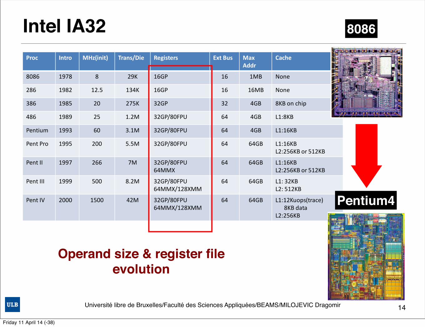
Intel IA32
14
8/05/2012'
1'
COMP3320/6464:'The'Intel'i86'Story'
'Jiri'Jaros,'Alistair'Rendell'and'Jun'Zhou'
__________________COMP3320)Lecture)1520)Copyright)©)2012)The)Australian)National)University_______________)
15.1'The'Intel'IAF32'Family'
Proc) Intro) MHz(init)) Trans/Die) Registers) Ext)Bus) Max)Addr)
Cache)
8086' 1978' 8' 29K' 16GP' 16' 1MB' None'
286' 1982' 12.5' 134K' 16GP' 16' 16MB' None'
386' 1985' 20' 275K' 32GP' 32' 4GB' 8KB'on'chip'
486' 1989' 25' 1.2M' 32GP/80FPU' 64' 4GB' L1:8KB'
Pentium' 1993' 60' 3.1M' 32GP/80FPU' 64' 4GB' L1:16KB'
Pent'Pro' 1995' 200' 5.5M' 32GP/80FPU' 64' 64GB' L1:16KB'L2:256KB'or'512KB'
Pent'II' 1997' 266' 7M' 32GP/80FPU'64MMX'
64' 64GB' L1:16KB'L2:256KB'or'512KB'
Pent'III' 1999' 500' 8.2M' 32GP/80FPU'64MMX/128XMM'
64' 64GB' L1:'32KB'L2:'512KB'
Pent'IV' 2000' 1500' 42M' 32GP/80FPU'64MMX/128XMM'
64' 64GB' L1:12Kuops(trace)'''''''8KB'data'L2:256KB'
__________________COMP3320)Lecture)1521)Copyright)©)2012)The)Australian)National)University_______________)
15.2'The'Intel'IAF32'and'Intel64'Family'
Proc) Intro) MHz(init)) Trans/Die) Registers) Ext)Bus) Max)Addr)
Cache)
Pent'M' 2003' 900' 140M' 32GP/80FPU'64MMX/128XMM'
64' 64GB' L1:'32KB'L2:'1M'
Core''(Duo)'
2006' 1500'1600'
228M' 32GP/80FPU'64MMX/128XMM'
64' 64GB' L1:'32KB'L2:'2M'
Core'2'(Duo/Quad)'
2006' 1600'2000'
410M'(2)'820M'(4)'
32GP/80FPU'64MMX/128XMM'
2x64' 1TB' L1:'32KB'L2:'2M/4M'or'6/12MB'
Nehalem''(2F8'cores)'
2008' 2660' 731M' 32GP/80FPU'64MMX/128XMM'
3x64' 256TB' L1:32KB'L2:256KB'L3:'4MBF12MB'
Sandy'Bridge'(2F8'cores)'
2011' 2800' 1.16G'(4)'2.27G'(8)'
32GP/80FPU'64MMX/128XMM'256YMM'
4x64' 256TB''
L1:32KB'L2:256KB'L3:'8MBF20MB'
__________________COMP3320)Lecture)1522)Copyright)©)2012)The)Australian)National)University_______________)
15.3'�����������Law'(1971F2011)'
__________________COMP3320)Lecture)1523)Copyright)©)2012)The)Australian)National)University_______________)
8/05/2012'
2'
15.4'Intel'4004'(1971),'2300'Transistors'
__________________COMP3320)Lecture)1524)Copyright)©)2012)The)Australian)National)University_______________)
15.5'Intel'8086'(1978),'29K'Transistors'
__________________COMP3320)Lecture)1525)Copyright)©)2012)The)Australian)National)University_______________)
15.6'Intel'80386'(1985),'275K'Transistors'
__________________COMP3320)Lecture)1526)Copyright)©)2012)The)Australian)National)University_______________)
15.7'Pentium'P6'Architecture'
� Pentium)P6)Architecture)is)basis)for)Pentium)Pro,)Pentium)II,))
and)Pentium)III.)
� Can)still)run)object)code)produced)for)Intel)processors)built)in)1978!!))
� item'it'carries'a'LOT'of'history!'
� 322bit)CISC)processor)with)RISC2like)micro2operations)
� Processor)and)cache)are)packaged)on)a)single)board)
� Two)level)cache)
� L1:'On'chip'J'16K'data'and'16K'instruction,'32'byte'cache'line'size,'4Jway'set'associative'
� L2:'Off'chip'J'256KBJ2MB'depending'on'exact'chip'(runs'at'half'clock'speed)''
'
� Just)one)floating)point)operation)per)cycle)
� general)purpose)registers)and)8)802bit)floating)point)registers)
__________________COMP3320)Lecture)1527)Copyright)©)2012)The)Australian)National)University_______________)
8/05/2012'
6'
15.20'Pentium'IV'(2000),'42M'transistors'
_________________COMP3320)Lecture)15220)Copyright)©)2012)The)Australian)National)University_______________)
15.21'Intel'Tic?Tock'Development'Model'
))))))))))
� Tick)) �)Process)technology)advancement)� Tock))�)New)microarchitecture)
_________________COMP3320)Lecture)15221)Copyright)©)2012)The)Australian)National)University_______________)
15.22'Intel'Core'Architecture'#1'� Intel®)Wide)Dynamic)Execution)(142stage)pipeline))
� Wider'execution'path'(four'(+)'�������'per'cycle)'� Advanced'branch'prediction'� Macro?fusion'
� Roughly'~15%'of'all'instructions'are'conditional'branches'� Macro?fusion'fuses'a'comparison'and'jump'to'reduce'micro?ops'running'down'the'pipeline'
� Micro?fusion'� Merges'the'load'and'operation'micro?ops'into'one'macro?op'
� 642Bit)Support)(Core)2))� Merom,'Conroe,'and'Wood'
� Intel®)Advanced)Memory)Access)� Improved'prefetching'� Memory'disambiguation'
� Advance'load'before'a'possible'data'dependency'(pointer'conflict)'� Earlier'loads'hide'memory'latencies'
_________________COMP3320)Lecture)15222)Copyright)©)2012)The)Australian)National)University_______________)
15.23'Intel'Core'Architecture'#2'� Intel®)Advanced)Smart)Cache:)Multi2core)optimization)
� Shared'between'the'two'cores'� Advanced'Transfer'Cache'architecture'� Reduced'bus'traffic'� Both'cores'have'full'access'to'the'entire'cache'� L1D'and'L2'cache'prefetching'
'
� Intelligent)Power)Capability):)Advanced)power)gating)&)Dynamic)power)coordination)� Multi?point'demand?based'switching'� Voltage?Frequency'switching'separation'� Supports'transitions'to'deeper'sleep'modes'� Event'blocking'� Clock'partitioning'and'recovery'� Dynamic'Bus'Parking'� During'periods'of'high'performance'execution,'many'parts'of'the'chip'core'can'be'shut''''
off'
_________________COMP3320)Lecture)15223)Copyright)©)2012)The)Australian)National)University_______________)
Operand size & register file evolution
8086
Pentium4
Friday 11 April 14 (-38)
Université libre de Bruxelles/Faculté des Sciences Appliquées/BEAMS/MILOJEVIC Dragomir
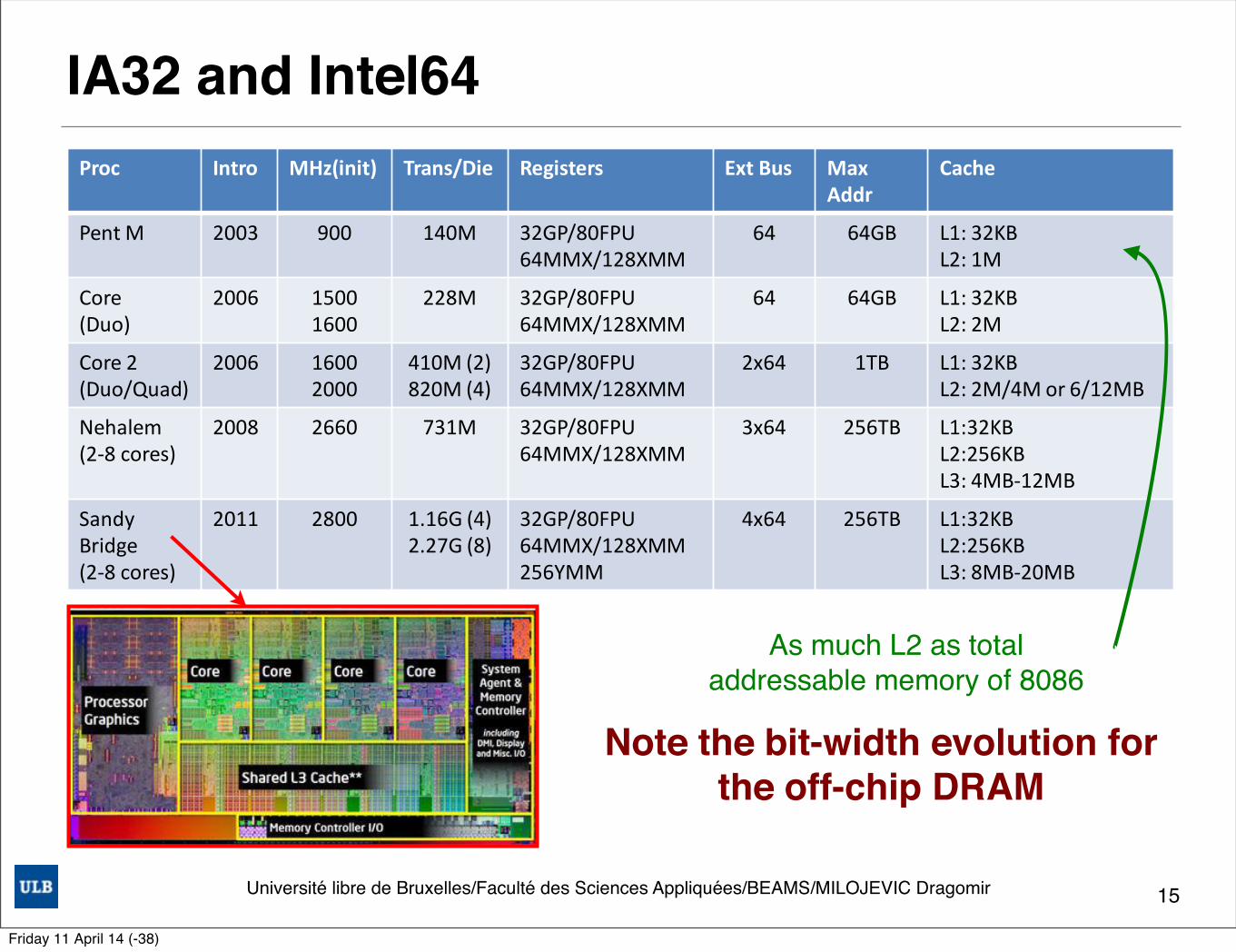
IA32 and Intel64
15
8/05/2012'
1'
COMP3320/6464:'The'Intel'i86'Story'
'Jiri'Jaros,'Alistair'Rendell'and'Jun'Zhou'
__________________COMP3320)Lecture)1520)Copyright)©)2012)The)Australian)National)University_______________)
15.1'The'Intel'IAF32'Family'
Proc) Intro) MHz(init)) Trans/Die) Registers) Ext)Bus) Max)Addr)
Cache)
8086' 1978' 8' 29K' 16GP' 16' 1MB' None'
286' 1982' 12.5' 134K' 16GP' 16' 16MB' None'
386' 1985' 20' 275K' 32GP' 32' 4GB' 8KB'on'chip'
486' 1989' 25' 1.2M' 32GP/80FPU' 64' 4GB' L1:8KB'
Pentium' 1993' 60' 3.1M' 32GP/80FPU' 64' 4GB' L1:16KB'
Pent'Pro' 1995' 200' 5.5M' 32GP/80FPU' 64' 64GB' L1:16KB'L2:256KB'or'512KB'
Pent'II' 1997' 266' 7M' 32GP/80FPU'64MMX'
64' 64GB' L1:16KB'L2:256KB'or'512KB'
Pent'III' 1999' 500' 8.2M' 32GP/80FPU'64MMX/128XMM'
64' 64GB' L1:'32KB'L2:'512KB'
Pent'IV' 2000' 1500' 42M' 32GP/80FPU'64MMX/128XMM'
64' 64GB' L1:12Kuops(trace)'''''''8KB'data'L2:256KB'
__________________COMP3320)Lecture)1521)Copyright)©)2012)The)Australian)National)University_______________)
15.2'The'Intel'IAF32'and'Intel64'Family'
Proc) Intro) MHz(init)) Trans/Die) Registers) Ext)Bus) Max)Addr)
Cache)
Pent'M' 2003' 900' 140M' 32GP/80FPU'64MMX/128XMM'
64' 64GB' L1:'32KB'L2:'1M'
Core''(Duo)'
2006' 1500'1600'
228M' 32GP/80FPU'64MMX/128XMM'
64' 64GB' L1:'32KB'L2:'2M'
Core'2'(Duo/Quad)'
2006' 1600'2000'
410M'(2)'820M'(4)'
32GP/80FPU'64MMX/128XMM'
2x64' 1TB' L1:'32KB'L2:'2M/4M'or'6/12MB'
Nehalem''(2F8'cores)'
2008' 2660' 731M' 32GP/80FPU'64MMX/128XMM'
3x64' 256TB' L1:32KB'L2:256KB'L3:'4MBF12MB'
Sandy'Bridge'(2F8'cores)'
2011' 2800' 1.16G'(4)'2.27G'(8)'
32GP/80FPU'64MMX/128XMM'256YMM'
4x64' 256TB''
L1:32KB'L2:256KB'L3:'8MBF20MB'
__________________COMP3320)Lecture)1522)Copyright)©)2012)The)Australian)National)University_______________)
15.3'�����������Law'(1971F2011)'
__________________COMP3320)Lecture)1523)Copyright)©)2012)The)Australian)National)University_______________)
Sandy Bridge 995 million transistors in a 216 m^2
Memory controller, the PCI Express (PCIe) controller, and video functions are all located within the processor die
Features• Uop Micro-operation Cache• Improved Branch Prediction • Advanced Vector Extensions (AVX)• The last level cache (LLC)• The System Agent• Turbo Boost• Quick Sync
Note the bit-width evolution forthe off-chip DRAM
As much L2 as total addressable memory of 8086
Friday 11 April 14 (-38)
Université libre de Bruxelles/Faculté des Sciences Appliquées/BEAMS/MILOJEVIC Dragomir
Intel’s future ?• Not very clear …• Desktop will not be there for a very long time• Market for high-performance micro-processors will most likely
dramatically shrink in the next few years :❖ It has been already some time that mobile market
(smart-phones + tablets) surpassed PC market
• Will data-center/server/high-performance computing be enough to feed the monster ? ✓ Very difficult to say … but we can have reasonable doubts✓ Sign for the winds of change is the fab opening✓ After all they did cut a deal with Apple ...
• Anyhow for 14, 10 and maybe 7nm they are going to be there for sure ...
16
Friday 11 April 14 (-38)
NetBurst micro-architecture(Pentium4)
Friday 11 April 14 (-38)
Université libre de Bruxelles/Faculté des Sciences Appliquées/BEAMS/MILOJEVIC Dragomir
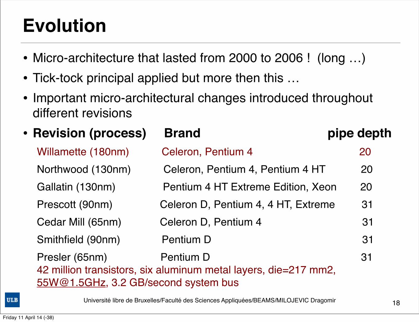
Evolution• Micro-architecture that lasted from 2000 to 2006 ! (long …)• Tick-tock principal applied but more then this …• Important micro-architectural changes introduced throughout
different revisions• Revision (process) Brand pipe depth
Willamette (180nm) Celeron, Pentium 4 20Northwood (130nm) Celeron, Pentium 4, Pentium 4 HT 20Gallatin (130nm) Pentium 4 HT Extreme Edition, Xeon 20Prescott (90nm) Celeron D, Pentium 4, 4 HT, Extreme 31Cedar Mill (65nm) Celeron D, Pentium 4 31Smithfield (90nm) Pentium D 31Presler (65nm) Pentium D 3142 million transistors, six aluminum metal layers, die=217 mm2, [email protected], 3.2 GB/second system bus
18
Friday 11 April 14 (-38)
Université libre de Bruxelles/Faculté des Sciences Appliquées/BEAMS/MILOJEVIC Dragomir
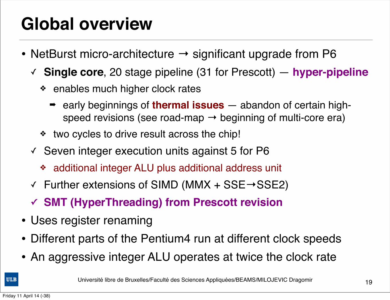
Global overview• NetBurst micro-architecture → significant upgrade from P6✓ Single core, 20 stage pipeline (31 for Prescott) — hyper-pipeline
❖ enables much higher clock rates ➡ early beginnings of thermal issues — abandon of certain high-
speed revisions (see road-map → beginning of multi-core era)❖ two cycles to drive result across the chip!
✓ Seven integer execution units against 5 for P6❖ additional integer ALU plus additional address unit
✓ Further extensions of SIMD (MMX + SSE→SSE2)✓ SMT (HyperThreading) from Prescott revision
• Uses register renaming • Different parts of the Pentium4 run at different clock speeds• An aggressive integer ALU operates at twice the clock rate
19
Friday 11 April 14 (-38)
Université libre de Bruxelles/Faculté des Sciences Appliquées/BEAMS/MILOJEVIC Dragomir
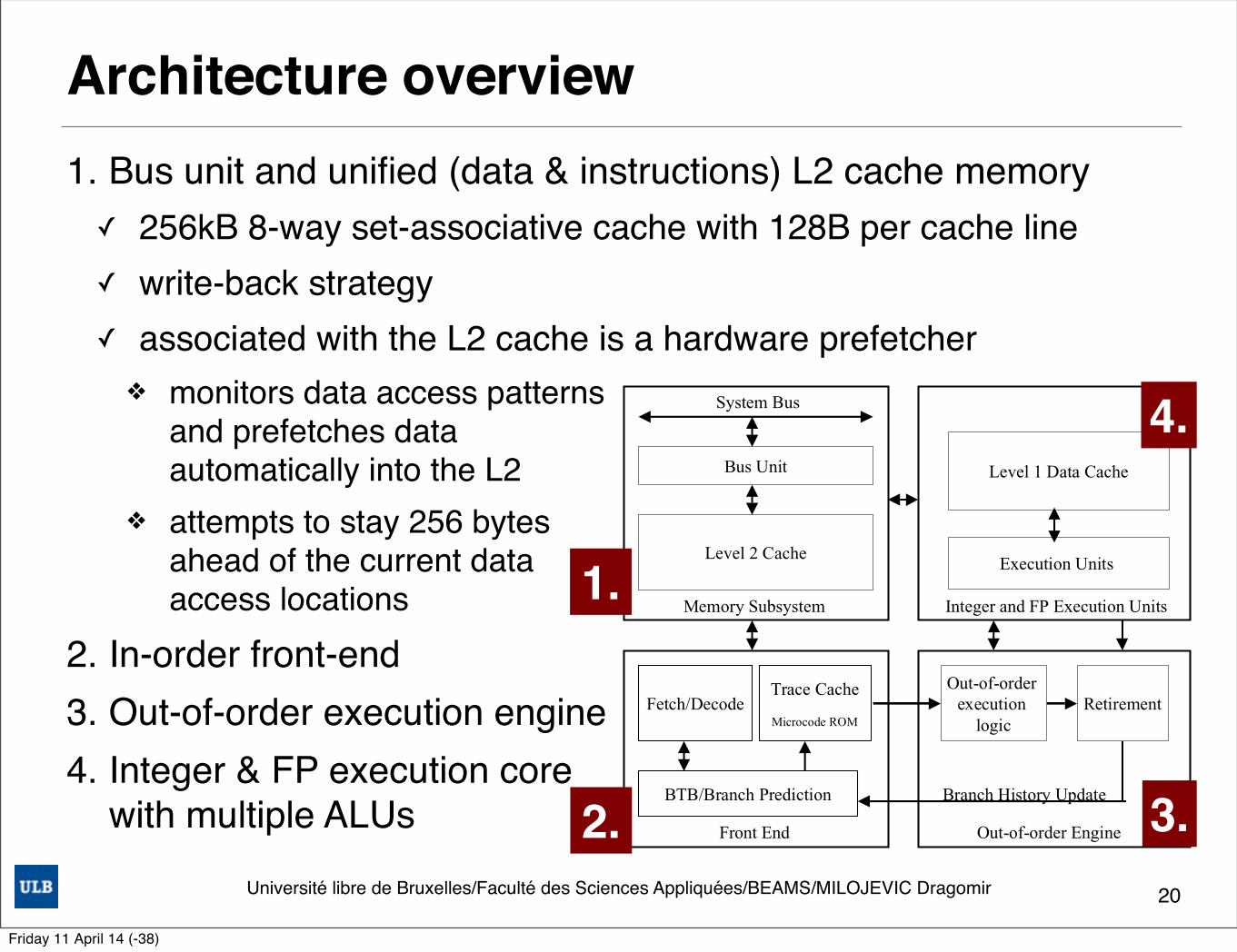
Architecture overview1. Bus unit and unified (data & instructions) L2 cache memory✓ 256kB 8-way set-associative cache with 128B per cache line✓ write-back strategy✓ associated with the L2 cache is a hardware prefetcher
❖ monitors data access patterns and prefetches data automatically into the L2
❖ attempts to stay 256 bytes ahead of the current data access locations
2. In-order front-end3. Out-of-order execution engine4. Integer & FP execution core
with multiple ALUs
20
Intel Technology Journal Q1, 2001
The Microarchitecture of the Pentium 4 Processor 2
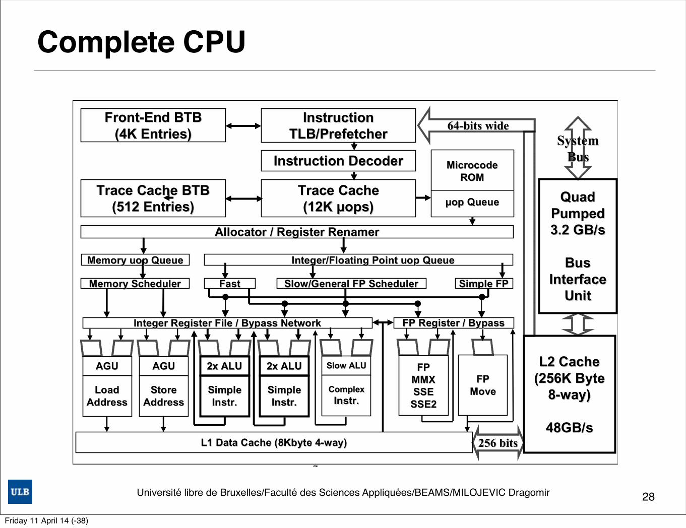
OVERVIEW OF THE NETBURST™ MICROARCHITECTURE A fast processor requires balancing and tuning of many microarchitectural features that compete for processor die cost and for design and validation efforts. Figure 1 shows the basic Intel NetBurst microarchitecture of the Pentium 4 processor. As you can see, there are four main sections: the in-order front end, the out-of-order execution engine, the integer and floating-point execution units, and the memory subsystem.
BTB/Branch Prediction
Out-of-order execution
logicRetirementFetch/Decode
Trace Cache
Microcode ROM
Front End
Branch History Update
Level 1 Data Cache
Execution Units
Bus Unit
Level 2 Cache
System Bus
Memory Subsystem
Out-of-order Engine
Integer and FP Execution Units
Figure 1: Basic block diagram
In-Order Front End The in-order front end is the part of the machine that fetches the instructions to be executed next in the program and prepares them to be used later in the machine pipeline. Its job is to supply a high-bandwidth stream of decoded instructions to the out-of-order execution core, which will do the actual completion of the instructions. The front end has highly accurate branch prediction logic that uses the past history of program execution to speculate where the program is going to execute next. The predicted instruction address, from this front-end branch prediction logic, is used to fetch instruction bytes from the Level 2 (L2) cache. These IA-32 instruction bytes are then decoded into basic operations called uops (micro-operations) that the execution core is able to execute.
The NetBurst microarchitecture has an advanced form of a Level 1 (L1) instruction cache called the Execution Trace Cache. Unlike conventional instruction caches, the Trace Cache sits between the instruction decode logic and the execution core as shown in Figure 1. In this location the Trace Cache is able to store the already decoded IA-32 instructions or uops. Storing already decoded instructions removes the IA-32 decoding from the main execution loop. Typically the instructions are decoded
once and placed in the Trace Cache and then used repeatedly from there like a normal instruction cache on previous machines. The IA-32 instruction decoder is only used when the machine misses the Trace Cache and needs to go to the L2 cache to get and decode new IA-32 instruction bytes.
Out-of-Order Execution Logic The out-of-order execution engine is where the instructions are prepared for execution. The out-of-order execution logic has several buffers that it uses to smooth and re-order the flow of instructions to optimize performance as they go down the pipeline and get scheduled for execution. Instructions are aggressively re-ordered to allow them to execute as quickly as their input operands are ready. This out-of-order execution allows instructions in the program following delayed instructions to proceed around them as long as they do not depend on those delayed instructions. Out-of-order execution allows the execution resources such as the ALUs and the cache to be kept as busy as possible executing independent instructions that are ready to execute.
The retirement logic is what reorders the instructions, executed in an out-of-order manner, back to the original program order. This retirement logic receives the completion status of the executed instructions from the execution units and processes the results so that the proper architectural state is committed (or retired) according to the program order. The Pentium 4 processor can retire up to three uops per clock cycle. This retirement logic ensures that exceptions occur only if the operation causing the exception is the oldest, non-retired operation in the machine. This logic also reports branch history information to the branch predictors at the front end of the machine so they can train with the latest known-good branch-history information.
Integer and Floating-Point Execution Units The execution units are where the instructions are actually executed. This section includes the register files that store the integer and floating-point data operand values that the instructions need to execute. The execution units include several types of integer and floating-point execution units that compute the results and also the L1 data cache that is used for most load and store operations.
Memory Subsystem Figure 1 also shows the memory subsystem. This includes the L2 cache and the system bus. The L2 cache stores both instructions and data that cannot fit in the Execution Trace Cache and the L1 data cache. The external system bus is connected to the backside of the second-level cache and is used to access main memory when the L2 cache has a cache miss, and to access the system I/O resources.
2.
1.
3.
4.
Friday 11 April 14 (-38)
Université libre de Bruxelles/Faculté des Sciences Appliquées/BEAMS/MILOJEVIC Dragomir
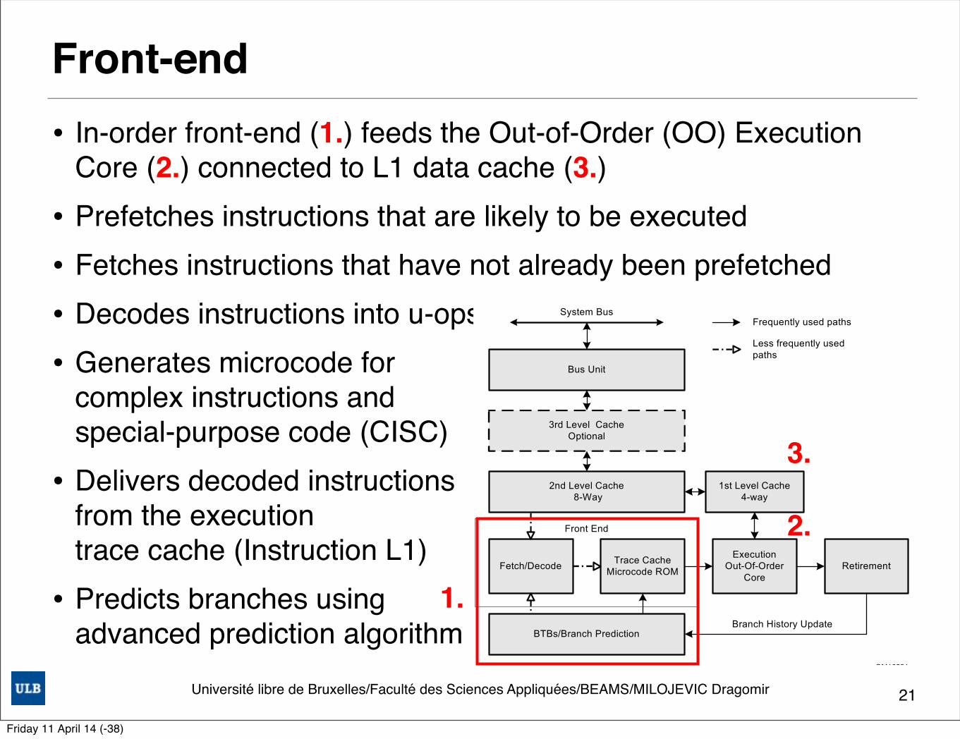
• In-order front-end (1.) feeds the Out-of-Order (OO) Execution Core (2.) connected to L1 data cache (3.)
• Prefetches instructions that are likely to be executed• Fetches instructions that have not already been prefetched• Decodes instructions into u-ops• Generates microcode for
complex instructions and special-purpose code (CISC)
• Delivers decoded instructions from the execution trace cache (Instruction L1)
• Predicts branches using advanced prediction algorithm
Front-end
21
Vol. 1 2-9
INTEL® 64 AND IA-32 ARCHITECTURES
2.2.2.1 The Front End Pipeline
The front end supplies instructions in program order to the out-of-order execution core. It performs a number of functions:• Prefetches instructions that are likely to be executed• Fetches instructions that have not already been prefetched• Decodes instructions into micro-operations• Generates microcode for complex instructions and special-purpose code• Delivers decoded instructions from the execution trace cache• Predicts branches using highly advanced algorithm
The pipeline is designed to address common problems in high-speed, pipelined microprocessors. Two of these problems contribute to major sources of delays:• time to decode instructions fetched from the target• wasted decode bandwidth due to branches or branch target in the middle of cache lines
The operation of the pipeline’s trace cache addresses these issues. Instructions are constantly being fetched and decoded by the translation engine (part of the fetch/decode logic) and built into sequences of µops called traces. At any time, multiple traces (representing prefetched branches) are being stored in the trace cache. The trace cache is searched for the instruction that follows the active branch. If the instruction also appears as the first instruction in a pre-fetched branch, the fetch and decode of instructions from the memory hierarchy ceases and the pre-fetched branch becomes the new source of instructions (see Figure 2-2).
The trace cache and the translation engine have cooperating branch prediction hardware. Branch targets are predicted based on their linear addresses using branch target buffers (BTBs) and fetched as soon as possible.
Figure 2-2. The Intel NetBurst Microarchitecture
Fetch/Decode Trace CacheMicrocode ROM
ExecutionOut-Of-Order
CoreRetirement
1st Level Cache4-way
2nd Level Cache 8-Way
BTBs/Branch Prediction
Bus Unit
System BusFrequently used paths
Less frequently usedpaths
Front End
3rd Level CacheOptional
Branch History Update
OM16521
3.
2.
1.
Friday 11 April 14 (-38)
Université libre de Bruxelles/Faculté des Sciences Appliquées/BEAMS/MILOJEVIC Dragomir
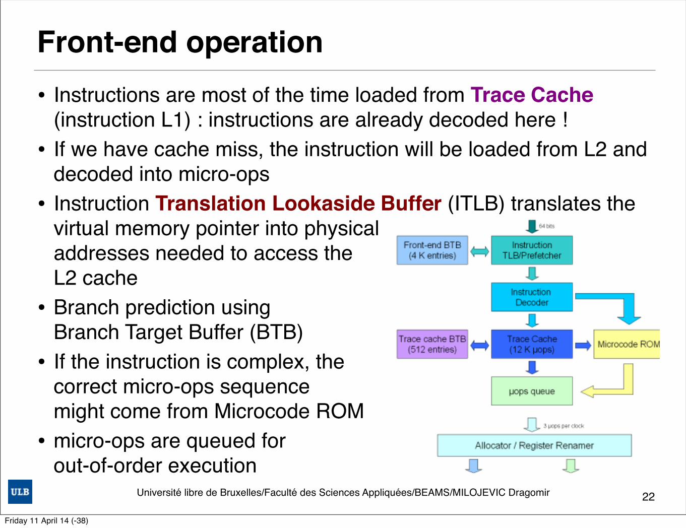
Front-end operation• Instructions are most of the time loaded from Trace Cache
(instruction L1) : instructions are already decoded here !• If we have cache miss, the instruction will be loaded from L2 and
decoded into micro-ops• Instruction Translation Lookaside Buffer (ITLB) translates the
virtual memory pointer into physicaladdresses needed to access the L2 cache
• Branch prediction using Branch Target Buffer (BTB)
• If the instruction is complex, the correct micro-ops sequence might come from Microcode ROM
• micro-ops are queued for out-of-order execution
22
8/05/2012'
5'
15.16'Pentium'IV'(NetBurst'Architecture)'#2'
� Replaces(L1(I,Cache(with(an(Instruction(Trace(Cache(containing(decoded(uops(
� Branch(target(buffer(eight(times(larger(with(improved(branch(prediction(algorithm(� very'long'pipeline'expensive'when'wrong'
� Extends(SIMD(instructions(with(streaming(SIMD(Extension(2((SSE2)(that(can(be(used(to(perform(double(precision(floating(point(arithmetic(� peak'FLOPS'is'now'2'times'clock'rate'NOT'1'as'for'Pentium'III'� to'achieve'this'currently'requires'use'of'Intel'Compiler'
� Greatly(improved(memory(bandwidth(via(400MHz(system(bus(� Adds(performance(counters!(� 1.7(GHz(Pentium(IV(outperforms(1GHz(Pentium(III(by(factor(of(1.26(for(
SEPC(CINT200,(but(1.8(for(SPEC(CFP2000(
_________________COMP3320(Lecture(15,16(Copyright(©(2012(The(Australian(National(University_______________(
15.17'Pentium'IV'MicroQArchitecture'
_________________COMP3320(Lecture(15,17(Copyright(©(2012(The(Australian(National(University_______________(
15.18'Pentium'IV'�'Front'End'
Allocate(a(ROB(entry((and(registers(or(L/S(buffer((
_________________COMP3320(Lecture(15,18(Copyright(©(2012(The(Australian(National(University_______________(
!
Instruction'loaded'from'L2'and'branch'prediction'using'BTB''
x86'instruction'decoded'into'�ops''
Decoded'instruction'read'from'TC'or'Microcode'ROM'into'the'�ops'queue''8'standard''x86'register'are'mapped'on'128'(FX'or'FP)'architecture'registers'
15.19'Pentium'IV'Scheduler'and'Execution'Units'
_________________COMP3320(Lecture(15,19(Copyright(©(2012(The(Australian(National(University_______________(
Friday 11 April 14 (-38)
Université libre de Bruxelles/Faculté des Sciences Appliquées/BEAMS/MILOJEVIC Dragomir
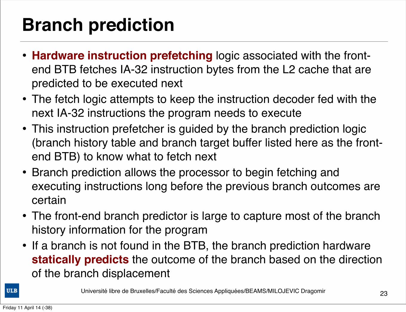
Branch prediction• Hardware instruction prefetching logic associated with the front-
end BTB fetches IA-32 instruction bytes from the L2 cache that are predicted to be executed next
• The fetch logic attempts to keep the instruction decoder fed with the next IA-32 instructions the program needs to execute
• This instruction prefetcher is guided by the branch prediction logic (branch history table and branch target buffer listed here as the front-end BTB) to know what to fetch next
• Branch prediction allows the processor to begin fetching and executing instructions long before the previous branch outcomes are certain
• The front-end branch predictor is large to capture most of the branch history information for the program
• If a branch is not found in the BTB, the branch prediction hardware statically predicts the outcome of the branch based on the direction of the branch displacement
23
Friday 11 April 14 (-38)

Université libre de Bruxelles/Faculté des Sciences Appliquées/BEAMS/MILOJEVIC Dragomir
Allocator• Out-of-order execution engine has buffers to perform its re-ordering,
tracking, and sequencing operations• Allocator logic allocates buffers needed by micro-op to execute• If a needed resource, such as a register file entry, is unavailable for one
of the three uops coming to the Allocator this clock cycle, the Allocator will stall this part of the machine
• When the resources become availablethe Allocator assigns them to the requesting uops and allows these satisfied uops to flow down the pipeline to be executed
• The Allocator also allocates one of the 128 integer or floating-point register entries for the result data value of the uop, and possibly a load or store buffer used to track one of the 48 loads or 24 stores in the machine pipeline
24
8/05/2012'
5'
15.16'Pentium'IV'(NetBurst'Architecture)'#2'
� Replaces(L1(I,Cache(with(an(Instruction(Trace(Cache(containing(decoded(uops(
� Branch(target(buffer(eight(times(larger(with(improved(branch(prediction(algorithm(� very'long'pipeline'expensive'when'wrong'
� Extends(SIMD(instructions(with(streaming(SIMD(Extension(2((SSE2)(that(can(be(used(to(perform(double(precision(floating(point(arithmetic(� peak'FLOPS'is'now'2'times'clock'rate'NOT'1'as'for'Pentium'III'� to'achieve'this'currently'requires'use'of'Intel'Compiler'
� Greatly(improved(memory(bandwidth(via(400MHz(system(bus(� Adds(performance(counters!(� 1.7(GHz(Pentium(IV(outperforms(1GHz(Pentium(III(by(factor(of(1.26(for(
SEPC(CINT200,(but(1.8(for(SPEC(CFP2000(
_________________COMP3320(Lecture(15,16(Copyright(©(2012(The(Australian(National(University_______________(
15.17'Pentium'IV'MicroQArchitecture'
_________________COMP3320(Lecture(15,17(Copyright(©(2012(The(Australian(National(University_______________(
15.18'Pentium'IV'�'Front'End'
Allocate(a(ROB(entry((and(registers(or(L/S(buffer((
_________________COMP3320(Lecture(15,18(Copyright(©(2012(The(Australian(National(University_______________(
!
Instruction'loaded'from'L2'and'branch'prediction'using'BTB''
x86'instruction'decoded'into'�ops''
Decoded'instruction'read'from'TC'or'Microcode'ROM'into'the'�ops'queue''8'standard''x86'register'are'mapped'on'128'(FX'or'FP)'architecture'registers'
15.19'Pentium'IV'Scheduler'and'Execution'Units'
_________________COMP3320(Lecture(15,19(Copyright(©(2012(The(Australian(National(University_______________(
Friday 11 April 14 (-38)
Université libre de Bruxelles/Faculté des Sciences Appliquées/BEAMS/MILOJEVIC Dragomir
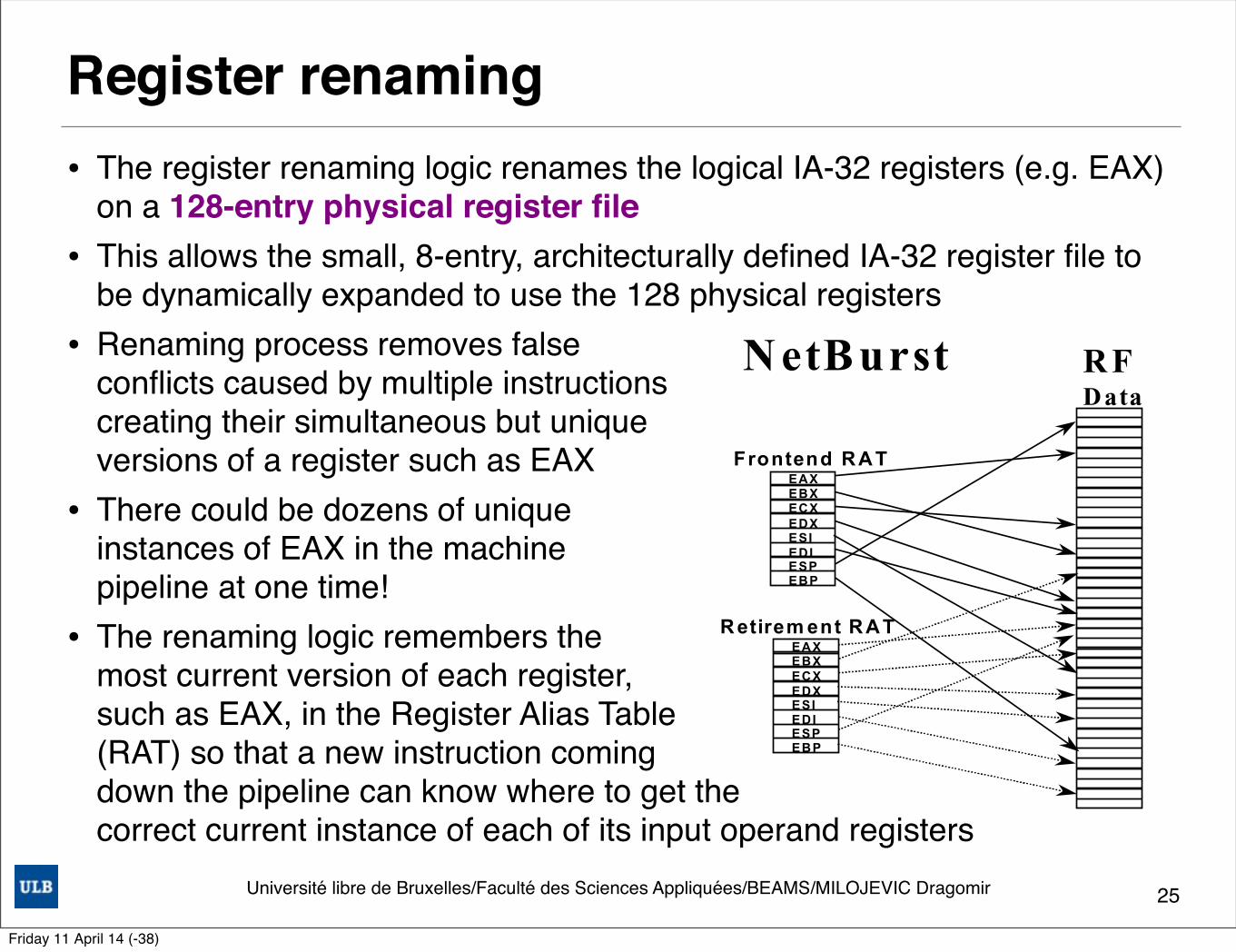
Register renaming• The register renaming logic renames the logical IA-32 registers (e.g. EAX)
on a 128-entry physical register file• This allows the small, 8-entry, architecturally defined IA-32 register file to
be dynamically expanded to use the 128 physical registers • Renaming process removes false
conflicts caused by multiple instructions creating their simultaneous but unique versions of a register such as EAX
• There could be dozens of unique instances of EAX in the machine pipeline at one time!
• The renaming logic remembers the most current version of each register, such as EAX, in the Register Alias Table (RAT) so that a new instruction coming down the pipeline can know where to get the correct current instance of each of its input operand registers
25
Intel Technology Journal Q1, 2001
The Microarchitecture of the Pentium 4 Processor 7
Pentium III N etBurst
R A TEAX
EBPESPEDIESIEDXECXEBX
R R F
R O BD ata Status
Frontend R A TEAX
EBPESPEDIESIEDXECXEBX
R etirem ent R A TEAX
EBPESPEDIESIEDXECXEBX
R O BStatus
R FD ata
Figure 5: Pentium® III vs. Pentium® 4 processor register allocation
The ROB entries, which track uop status, consist only of the status field and are allocated and deallocated sequentially. A sequence number assigned to each uop indicates its relative age. The sequence number points to the uop’s entry in the ROB array, which is similar to the P6 microarchitecture. The Register File entry is allocated from a list of available registers in the 128-entry RF–not sequentially like the ROB entries. Upon retirement, no result data values are actually moved from one physical structure to another.
Uop Scheduling The uop schedulers determine when a uop is ready to execute by tracking its input register operands. This is the heart of the out-of-order execution engine. The uop schedulers are what allow the instructions to be reordered to execute as soon as they are ready, while still maintaining the correct dependencies from the original program. The NetBurst microarchitecture has two sets of structures to aid in uop scheduling: the uop queues and the actual uop schedulers.
There are two uop queues–one for memory operations (loads and stores) and one for non-memory operations. Each of these queues stores the uops in strict FIFO (first-in, first-out) order with respect to the uops in its own queue, but each queue is allowed to be read out-of-order with respect to the other queue. This allows the dynamic out-of-order scheduling window to be larger than just having the uop schedulers do all the reordering work.
There are several individual uop schedulers that are used to schedule different types of uops for the various execution units on the Pentium 4 processor as shown in Figure 6. These schedulers determine when uops are ready to execute based on the readiness of their dependent input register operand sources and the availability of the execution resources the uops need to complete their operation.
These schedulers are tied to four different dispatch ports. There are two execution unit dispatch ports labeled port 0 and port 1 in Figure 6. These ports are fast: they can dispatch up to two operations each main processor clock cycle. Multiple schedulers share each of these two dispatch ports. The fast ALU schedulers can schedule on each half of the main clock cycle while the other schedulers can only schedule once per main processor clock cycle. They arbitrate for the dispatch port when multiple schedulers have ready operations at once. There is also a load and a store dispatch port that can dispatch a ready load and store each clock cycle. Collectively, these uop dispatch ports can dispatch up to six uops each main clock cycle. This dispatch bandwidth exceeds the front-end and retirement bandwidth, of three uops per clock, to allow for peak bursts of greater than 3 uops per clock and to allow higher flexibility in issuing uops to different dispatch ports. Figure 6 also shows the types of operations that can be dispatched to each port each clock cycle.
Friday 11 April 14 (-38)
Université libre de Bruxelles/Faculté des Sciences Appliquées/BEAMS/MILOJEVIC Dragomir
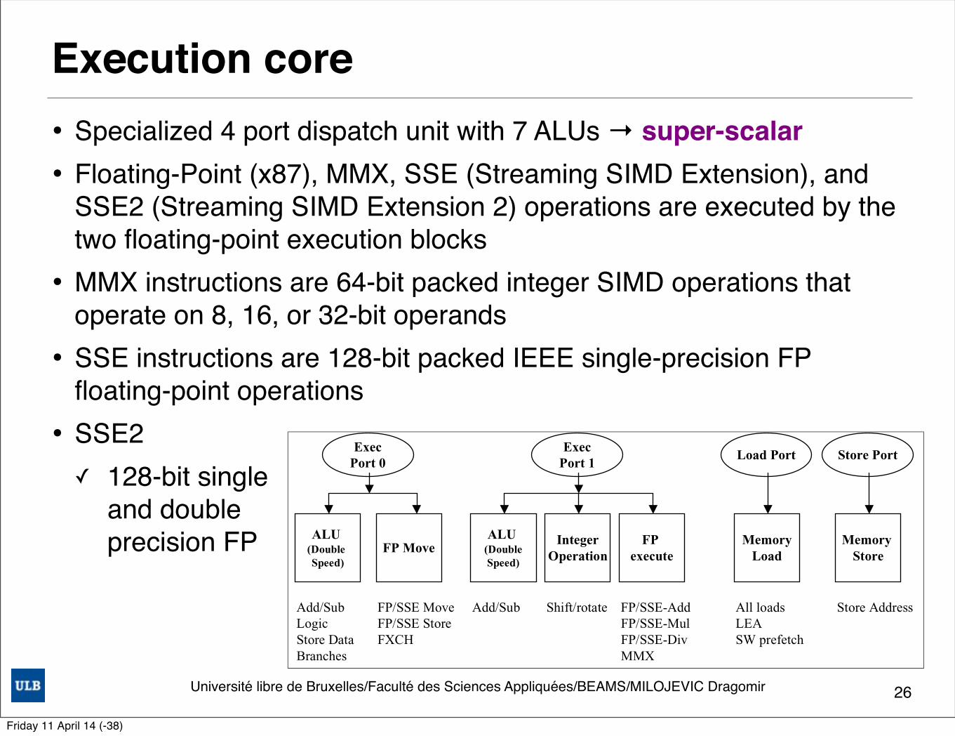
Execution core• Specialized 4 port dispatch unit with 7 ALUs → super-scalar• Floating-Point (x87), MMX, SSE (Streaming SIMD Extension), and
SSE2 (Streaming SIMD Extension 2) operations are executed by the two floating-point execution blocks
• MMX instructions are 64-bit packed integer SIMD operations that operate on 8, 16, or 32-bit operands
• SSE instructions are 128-bit packed IEEE single-precision FP floating-point operations
• SSE2✓ 128-bit single
and double precision FP
26
Intel Technology Journal Q1, 2001
The Microarchitecture of the Pentium 4 Processor 8
ExecPort 0
ExecPort 1
Load Port Store Port
ALU (Double Speed)
FP MoveMemory
LoadMemory
StoreFP
executeInteger
Operation
ALU (DoubleSpeed)
Add/SubLogicStore DataBranches
FP/SSE MoveFP/SSE StoreFXCH
Add/Sub Shift/rotate FP/SSE-AddFP/SSE-MulFP/SSE-DivMMX
All loadsLEASW prefetch
Store Address
Figure 6: Dispatch ports in the Pentium® 4 processor
Integer and Floating-Point Execution Units The execution units are where the instructions are actually executed. The execution units are designed to optimize overall performance by handling the most common cases as fast as possible. There are several different execution units in the NetBurst microarchitecture. The units used to execute integer operations include the low-latency integer ALUs, the complex integer instruction unit, the load and store address generation units, and the L1 data cache.
Floating-Point (x87), MMX, SSE (Streaming SIMD Extension), and SSE2 (Streaming SIMD Extension 2) operations are executed by the two floating-point execution blocks. MMX instructions are 64-bit packed integer SIMD operations that operate on 8, 16, or 32-bit operands. The SSE instructions are 128-bit packed IEEE single-precision floating-point operations. The Pentium 4 processor adds new forms of 128-bit SIMD instructions called SSE2. The SSE2 instructions support 128-bit packed IEEE double-precision SIMD floating-point operations and 128-bit packed integer SIMD operations. The packed integer operations support 8, 16, 32, and 64-bit operands. See IA-32 Intel Architecture Software Developer’s Manual Volume 1: Basic Architecture [3] for more detail on these SIMD operations.
The Integer and floating-point register files sit between the schedulers and the execution units. There is a separate 128-entry register file for both the integer and the floating-point/SSE operations. Each register file also has a multi-clock bypass network that bypasses or forwards just-completed results, which have not yet been written into the register file, to the new dependent uops. This multi-clock bypass network is needed because of the very high frequency of the design.
Low Latency Integer ALU The Pentium 4 processor execution units are designed to optimize overall performance by handling the most common cases as fast as possible. The Pentium 4 processor can do fully dependent ALU operations at twice the main clock rate. The ALU-bypass loop is a key closed loop in the processor pipeline. Approximately 60-70% of all uops in typical integer programs use this key integer ALU loop. Executing these operations at ! the latency of the main clock helps speed up program execution for most programs. Doing the ALU operations in one half a clock cycle does not buy a 2x performance increase, but it does improve the performance for most integer applications.
This high-speed ALU core is kept as small as possible to minimize the metal length and loading. Only the essential hardware necessary to perform the frequent ALU operations is included in this high-speed ALU execution loop. Functions that are not used very frequently, for most integer programs, are not put in this key low-latency ALU loop but are put elsewhere. Some examples of integer execution hardware put elsewhere are the multiplier, shifts, flag logic, and branch processing.
The processor does ALU operations with an effective latency of one-half of a clock cycle. It does this operation in a sequence of three fast clock cycles (the fast clock runs at 2x the main clock rate) as shown in Figure 7. In the first fast clock cycle, the low order 16-bits are computed and are immediately available to feed the low 16-bits of a dependent operation the very next fast clock cycle. The high-order 16 bits are processed in the next fast cycle, using the carry out just generated by the low 16-bit operation. This upper 16-bit result will be available to the next dependent operation exactly when needed. This is called a staggered add. The ALU flags
Friday 11 April 14 (-38)
Université libre de Bruxelles/Faculté des Sciences Appliquées/BEAMS/MILOJEVIC Dragomir
micro-op scheduling• The micro-op schedulers determine when a micro-op is ready to
execute by tracking its input register operands• They reorder instructions to execute as soon as they are
ready:✓ uop queues : store in FIFO fashion but read in out-of-order
❖ For memory operations❖ For non-memory operations (computation)
• Schedulers are tied to four different dispatch ports• There are two fast exec units dispatch ports: Port0 & Port1✓ fast: they can dispatch up to two operations each main
processor clock cycle• Multiple schedulers share each of these two dispatch ports• Other schedulers can only schedule once per main processor
clock cycle• There is also a load and a store schedule
27
Friday 11 April 14 (-38)
Université libre de Bruxelles/Faculté des Sciences Appliquées/BEAMS/MILOJEVIC Dragomir
Complete CPU
28
Intel Technology Journal Q1, 2001
The Microarchitecture of the Pentium 4 Processor 4
11 22 33 44 55 66 77 88 99 1010FetchFetch FetchFetch DecodeDecode DecodeDecode DecodeDecode RenameRename ROB RdROB Rd RdyRdy/Sch/Sch DispatchDispatch ExecExec
Basic Pentium III Processor Basic Pentium III Processor MispredictionMisprediction Pipeline Pipeline
Basic Pentium 4 Processor Basic Pentium 4 Processor MispredictionMisprediction Pipeline Pipeline
11 22 33 44 55 66 77 88 99 1010 1111 1212TC TC Nxt Nxt IPIP TC FetchTC Fetch DriveDrive AllocAlloc RenameRename QueQue SchSch SchSch SchSch
1313 1414DispDisp DispDisp
1515 1616 1717 1818 1919 2020RFRF ExEx FlgsFlgs Br CkBr Ck Drive DriveRF RF
Figure 3: Misprediction Pipeline
Allocator / Register RenamerAllocator / Register Renamer
Memory Memory uopuop Queue Queue Integer/Floating Point Integer/Floating Point uop uop QueueQueue
FP Register / BypassFP Register / Bypass
FPFPMMXMMXSSESSESSE2SSE2
FPFPMoveMove
Simple FPSimple FP
L1 Data Cache (8Kbyte 4-way)L1 Data Cache (8Kbyte 4-way)
Memory SchedulerMemory Scheduler FastFast Slow/General FP SchedulerSlow/General FP Scheduler
Integer Register File / Bypass NetworkInteger Register File / Bypass Network
ComplexComplexInstr.Instr.
Slow ALUSlow ALU
SimpleSimpleInstr.Instr.
2x ALU2x ALU
SimpleSimpleInstr.Instr.
2x ALU2x ALU
LoadLoadAddressAddress
AGUAGU
StoreStoreAddressAddress
AGUAGU
256 bits256 bits
64-bits wide64-bits wide
QuadQuadPumpedPumped3.2 GB/s3.2 GB/s
BusBusInterfaceInterface
UnitUnit
SystemSystemBusBus
L2 CacheL2 Cache(256K Byte(256K Byte
8-way)8-way)
48GB/s48GB/s
InstructionInstructionTLB/TLB/PrefetcherPrefetcher
Front-End BTBFront-End BTB(4K Entries)(4K Entries)
Instruction DecoderInstruction Decoder
Trace CacheTrace Cache(12K (12K µµopsops))
Trace Cache BTBTrace Cache BTB(512 Entries)(512 Entries)
MicrocodeMicrocodeROMROM
µµopop Queue Queue
Figure 4: Pentium® 4 processor microarchitecture
NETBURST MICROARCHITECTURE Figure 4 shows a more detailed block diagram of the NetBurst microarchitecture of the Pentium 4 processor. The top-left portion of the diagram shows the front end of the machine. The middle of the diagram illustrates the out-of-order buffering logic, and the bottom of the diagram shows the integer and floating-point execution units and the L1 data cache. On the right of the diagram is the memory subsystem.
Front End The front end of the Pentium 4 processor consists of several units as shown in the upper part of Figure 4. It has the Instruction TLB (ITLB), the front-end branch predictor (labeled here Front-End BTB), the IA-32 Instruction Decoder, the Trace Cache, and the Microcode ROM.
Friday 11 April 14 (-38)
Dragomir [email protected]
ELEC-H-473Microprocessor architecture
Intel x86 micro-architectureIvy/Sandy Bridge
Lecture 10,11
Friday 11 April 14 (-38)
Sandy & Ivy BridgeMicro-architectures
Friday 11 April 14 (-38)
Université libre de Bruxelles/Faculté des Sciences Appliquées/BEAMS/MILOJEVIC Dragomir
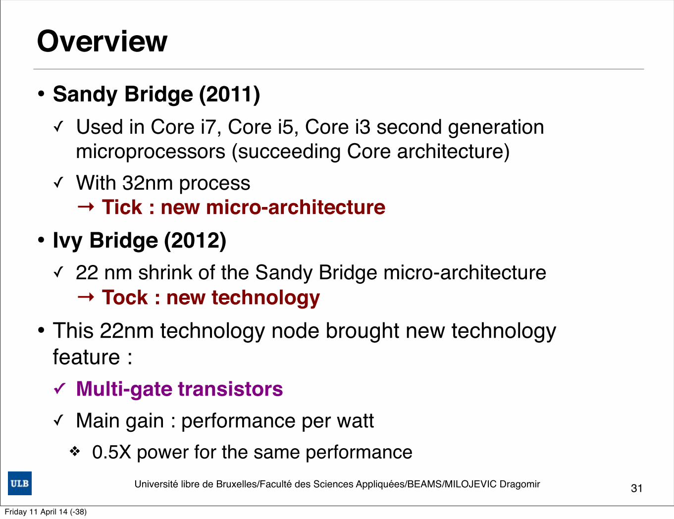
Overview• Sandy Bridge (2011)✓ Used in Core i7, Core i5, Core i3 second generation
microprocessors (succeeding Core architecture)✓ With 32nm process → Tick : new micro-architecture
• Ivy Bridge (2012)✓ 22 nm shrink of the Sandy Bridge micro-architecture → Tock : new technology
• This 22nm technology node brought new technology feature :✓ Multi-gate transistors ✓ Main gain : performance per watt
❖ 0.5X power for the same performance31
Friday 11 April 14 (-38)
Université libre de Bruxelles/Faculté des Sciences Appliquées/BEAMS/MILOJEVIC Dragomir
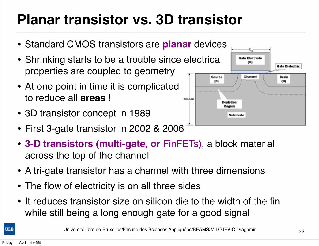
Planar transistor vs. 3D transistor• Standard CMOS transistors are planar devices• Shrinking starts to be a trouble since electrical
properties are coupled to geometry • At one point in time it is complicated
to reduce all areas !• 3D transistor concept in 1989• First 3-gate transistor in 2002 & 2006• 3-D transistors (multi-gate, or FinFETs), a block material
across the top of the channel• A tri-gate transistor has a channel with three dimensions• The flow of electricity is on all three sides• It reduces transistor size on silicon die to the width of the fin
while still being a long enough gate for a good signal32
Friday 11 April 14 (-38)
Université libre de Bruxelles/Faculté des Sciences Appliquées/BEAMS/MILOJEVIC Dragomir
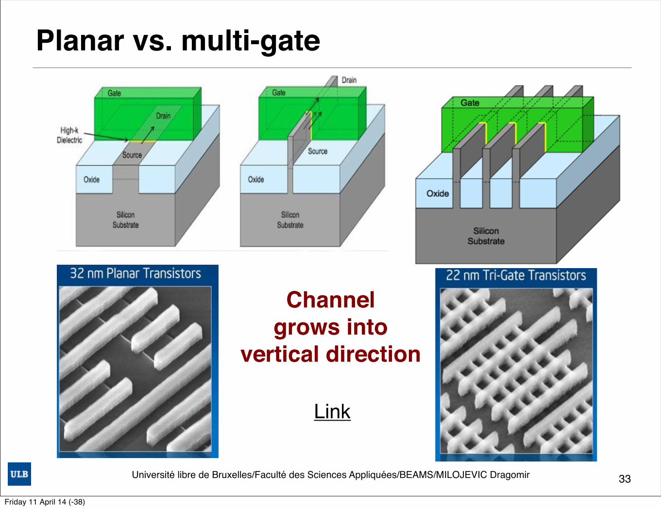
Planar vs. multi-gate
33
3D Tri-gate Transistors“The easiest way to imagine a Tri-Gate
transistor is to think of it as a normal transistor folded up in the middle”
•Ivy bridge's three sides of the channel equate to 22 nm (transistor width = 2H + w)•3-D concept Digh Hisamoto MuGFet in 1989•First tri-gate transistor was made by Ghau and Kayalieros in 2002 and 2006.•3-D transistors are known as FinFET, a block material across the top of the channel•A tri-gate transistor has a channel with three dimensions. The flow of electricity is on all three sides. It reduces transistor size on silicon die to the width of the fin while still being a long enough gate for a good signal.
Channelgrows into
vertical direction
Link
3D Tri-gate Transistors“The easiest way to imagine a Tri-Gate
transistor is to think of it as a normal transistor folded up in the middle”
•Ivy bridge's three sides of the channel equate to 22 nm (transistor width = 2H + w)•3-D concept Digh Hisamoto MuGFet in 1989•First tri-gate transistor was made by Ghau and Kayalieros in 2002 and 2006.•3-D transistors are known as FinFET, a block material across the top of the channel•A tri-gate transistor has a channel with three dimensions. The flow of electricity is on all three sides. It reduces transistor size on silicon die to the width of the fin while still being a long enough gate for a good signal.
Friday 11 April 14 (-38)
SandyBridge :micro-architecture overview
Friday 11 April 14 (-38)
Université libre de Bruxelles/Faculté des Sciences Appliquées/BEAMS/MILOJEVIC Dragomir
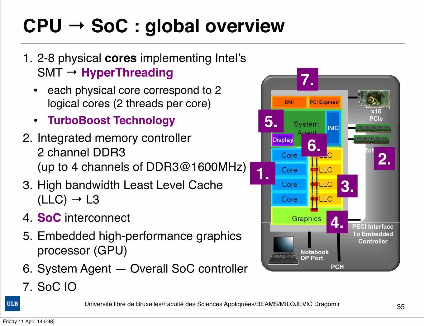
CPU → SoC : global overview1. 2-8 physical cores implementing Intel’s
SMT → HyperThreading• each physical core correspond to 2
logical cores (2 threads per core)• TurboBoost Technology
2. Integrated memory controller 2 channel DDR3 (up to 4 channels of DDR3@1600MHz)
3. High bandwidth Least Level Cache (LLC) → L3
4. SoC interconnect5. Embedded high-performance graphics
processor (GPU)6. System Agent — Overall SoC controller7. SoC IO
35
2
Sandy Bridge: Overview
Sandy Bridge - Intel® Next Generation Microarchitecture
Integrated Memory Controller 2ch DDR3
High Bandwidth Last Level Cache
Next Generation Processor Graphics and Media
Next Generation Intel® Turbo Boost Technology
Intel® Hyper-Threading Technology
4 Cores / 8 Threads 2 Cores / 4 Threads
Integrates CPU, Graphics, MC, PCI Express* On Single Chip
Embedded Display Port
Substantial performance improvement
Intel® Advanced Vector Extension (Intel® AVX)
High BW/low-latency modular core/GFX interconnect
Discrete Graphics Support: 1x16 or 2x8
2ch DDR3
x16 PCIe
PECI InterfaceTo Embedded
Controller
NotebookDP Port
PCH
Energy Efficiency
Stunning PerformanceStunning Performance
2.1.
3.
4.
5.6.
7.
Friday 11 April 14 (-38)
Université libre de Bruxelles/Faculté des Sciences Appliquées/BEAMS/MILOJEVIC Dragomir
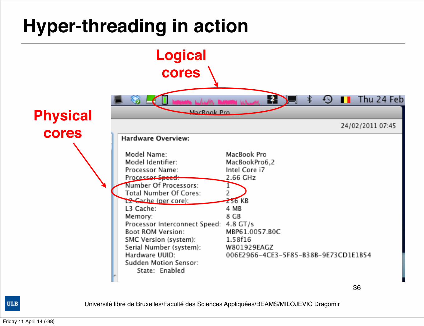
Hyper-threading in action
36
Physical cores
Logical cores
Friday 11 April 14 (-38)
Université libre de Bruxelles/Faculté des Sciences Appliquées/BEAMS/MILOJEVIC Dragomir
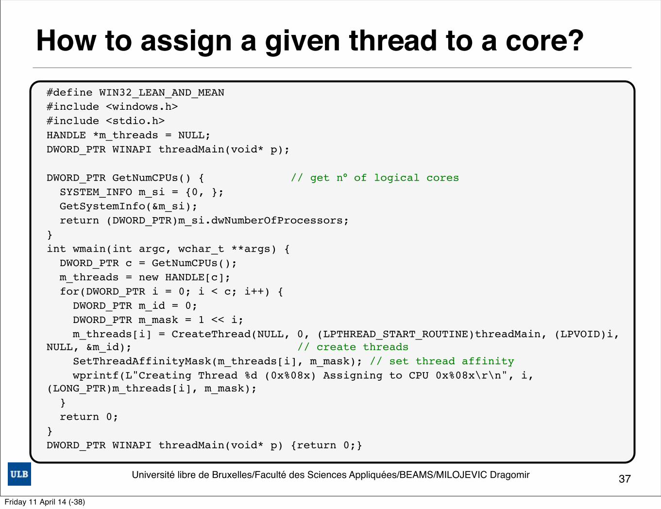
How to assign a given thread to a core?
37
#define WIN32_LEAN_AND_MEAN#include <windows.h>#include <stdio.h>HANDLE *m_threads = NULL;DWORD_PTR WINAPI threadMain(void* p);
DWORD_PTR GetNumCPUs() { // get n° of logical cores SYSTEM_INFO m_si = {0, }; GetSystemInfo(&m_si); return (DWORD_PTR)m_si.dwNumberOfProcessors;}int wmain(int argc, wchar_t **args) { DWORD_PTR c = GetNumCPUs(); m_threads = new HANDLE[c]; for(DWORD_PTR i = 0; i < c; i++) { DWORD_PTR m_id = 0; DWORD_PTR m_mask = 1 << i; m_threads[i] = CreateThread(NULL, 0, (LPTHREAD_START_ROUTINE)threadMain, (LPVOID)i, NULL, &m_id); // create threads SetThreadAffinityMask(m_threads[i], m_mask); // set thread affinity wprintf(L"Creating Thread %d (0x%08x) Assigning to CPU 0x%08x\r\n", i, (LONG_PTR)m_threads[i], m_mask); } return 0;}DWORD_PTR WINAPI threadMain(void* p) {return 0;}
Friday 11 April 14 (-38)
Université libre de Bruxelles/Faculté des Sciences Appliquées/BEAMS/MILOJEVIC Dragomir
Turbo Boost • Le CPU has few operating points in terms of Vdd, F
✓ Depending on the Vdd we can chose F
❖ Higher Vdd → higher operating F
✓ But both have impact on power since :
❖ P = C x Vdd2 x F
• TurboBoost : allows cores to run much faster then nominal operating F for a very short amount of time
• Idea behind : uses thermal inertia of the IC + package !
✓ Much slower then processing bursts
✓ Uses whole IC as kind of a heat spreader/sink
38
Friday 11 April 14 (-38)
Université libre de Bruxelles/Faculté des Sciences Appliquées/BEAMS/MILOJEVIC Dragomir
DDR IO — solving memory bottleneck• Embedded DDR-DRAM Controller• 2 (up to 4) independent channels for DDR3 & DDR3L
support✓ Low voltage DDR3 (DDR3L) support for mobile
• DDR Over-clocking✓ support for up to 2800 MT/s (up from 2133) ✓ Finer grain steps in adjusting frequency✓ Added 200 MHz
• DDR I/O embedded power gating✓ Power off DDR I/O when idle
39
Friday 11 April 14 (-38)
Université libre de Bruxelles/Faculté des Sciences Appliquées/BEAMS/MILOJEVIC Dragomir
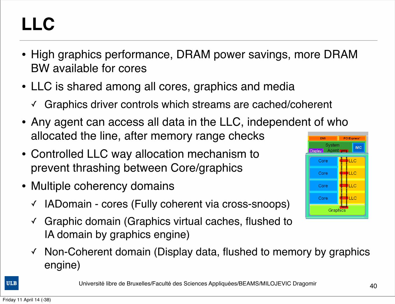
LLC• High graphics performance, DRAM power savings, more DRAM
BW available for cores• LLC is shared among all cores, graphics and media✓ Graphics driver controls which streams are cached/coherent
• Any agent can access all data in the LLC, independent of who allocated the line, after memory range checks
• Controlled LLC way allocation mechanism to prevent thrashing between Core/graphics
• Multiple coherency domains ✓ IADomain - cores (Fully coherent via cross-snoops)✓ Graphic domain (Graphics virtual caches, flushed to
IA domain by graphics engine)✓ Non-Coherent domain (Display data, flushed to memory by graphics
engine)
40
45
Sandy Bridge LLC Sharing• LLC shared among all Cores, Graphics and Media– Graphics driver controls which streams are cached/coherent– Any agent can access all data in the LLC, independent of who
allocated the line, after memory range checks• Controlled LLC way allocation mechanism to prevent
thrashing between Core/graphics• Multiple coherency domains– IA Domain (Fully coherent via cross-snoops)– Graphic domain (Graphics virtual caches,
flushed to IA domain by graphics engine)– Non-Coherent domain (Display data, flushed to
memory by graphics engine)
Block Diagram Illustrative only. Number of processor cores will vary with different processor models based on the Sandy Bridge Microarchitecture. Represents client processor implementation. Sandy Bridge - Intel® Next Generation Microarchitecture
Much higher Graphics performance, DRAM power savings, more DRAM BW
available for Cores
Friday 11 April 14 (-38)
Université libre de Bruxelles/Faculté des Sciences Appliquées/BEAMS/MILOJEVIC Dragomir
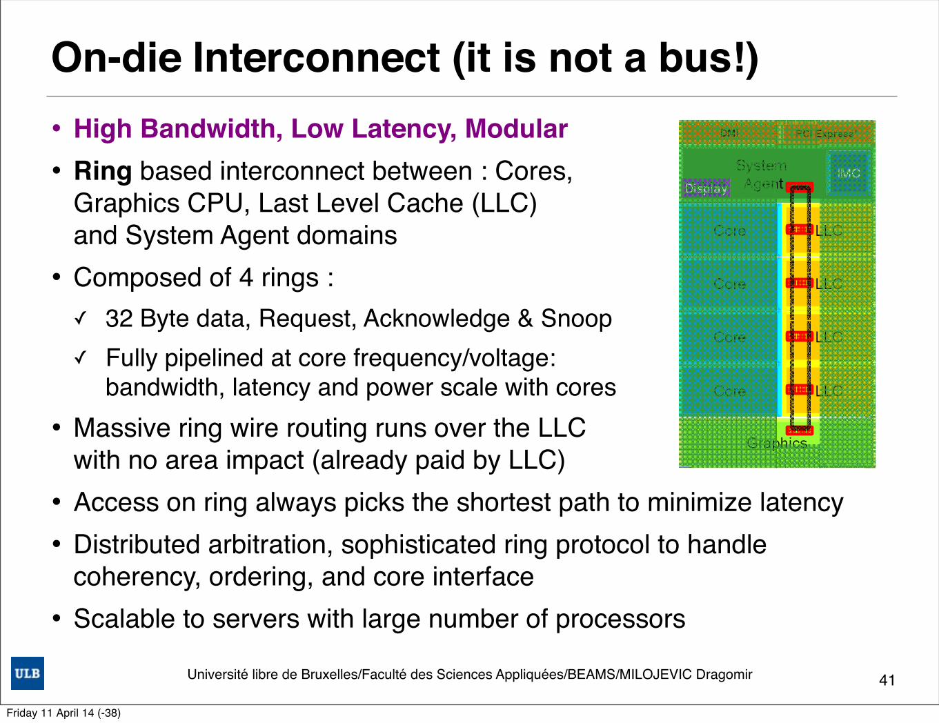
On-die Interconnect (it is not a bus!)• High Bandwidth, Low Latency, Modular• Ring based interconnect between : Cores,
Graphics CPU, Last Level Cache (LLC) and System Agent domains
• Composed of 4 rings :✓ 32 Byte data, Request, Acknowledge & Snoop ✓ Fully pipelined at core frequency/voltage:
bandwidth, latency and power scale with cores• Massive ring wire routing runs over the LLC
with no area impact (already paid by LLC)• Access on ring always picks the shortest path to minimize latency• Distributed arbitration, sophisticated ring protocol to handle
coherency, ordering, and core interface• Scalable to servers with large number of processors
41
28
Scalable Ring On-die Interconnect• Ring-based interconnect between Cores, Graphics, Last
Level Cache (LLC) and System Agent domain• Composed of 4 rings
– 32 Byte Data ring, Request ring, Acknowledgering and Snoop ring
– Fully pipelined at core frequency/voltage:bandwidth, latency and power scale with cores
• Massive ring wire routing runs over the LLC with no area impact
• Access on ring always picks the shortest path – minimize latency
• Distributed arbitration, sophisticated ring protocol to handle coherency, ordering, and core interface
• Scalable to servers with large number of processors
Block Diagram Illustrative only. Number of processor cores will vary with different processor models based on the Sandy Bridge Microarchitecture. Represents client processor implementation.
High Bandwidth, Low Latency, Modular
Friday 11 April 14 (-38)
Université libre de Bruxelles/Faculté des Sciences Appliquées/BEAMS/MILOJEVIC Dragomir
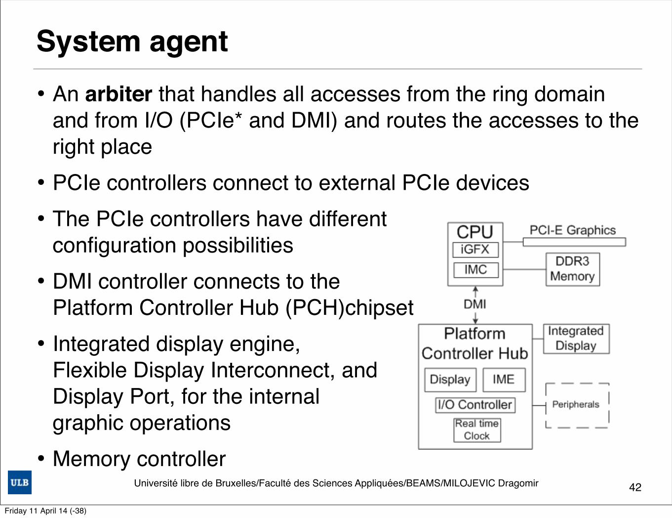
System agent• An arbiter that handles all accesses from the ring domain
and from I/O (PCIe* and DMI) and routes the accesses to the right place
• PCIe controllers connect to external PCIe devices• The PCIe controllers have different
configuration possibilities• DMI controller connects to the
Platform Controller Hub (PCH)chipset• Integrated display engine,
Flexible Display Interconnect, and Display Port, for the internal graphic operations
• Memory controller42
Friday 11 April 14 (-38)
Université libre de Bruxelles/Faculté des Sciences Appliquées/BEAMS/MILOJEVIC Dragomir
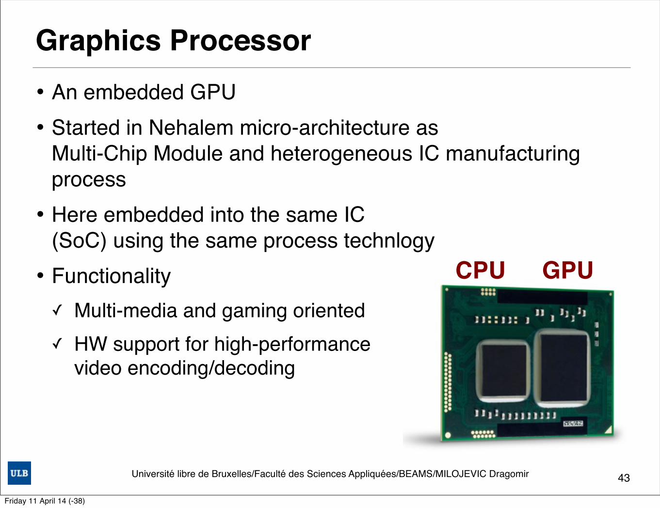
• An embedded GPU• Started in Nehalem micro-architecture as
Multi-Chip Module and heterogeneous IC manufacturing process
• Here embedded into the same IC (SoC) using the same process technlogy
• Functionality ✓ Multi-media and gaming oriented✓ HW support for high-performance
video encoding/decoding
Graphics Processor
43
CPU GPU
Friday 11 April 14 (-38)
Université libre de Bruxelles/Faculté des Sciences Appliquées/BEAMS/MILOJEVIC Dragomir
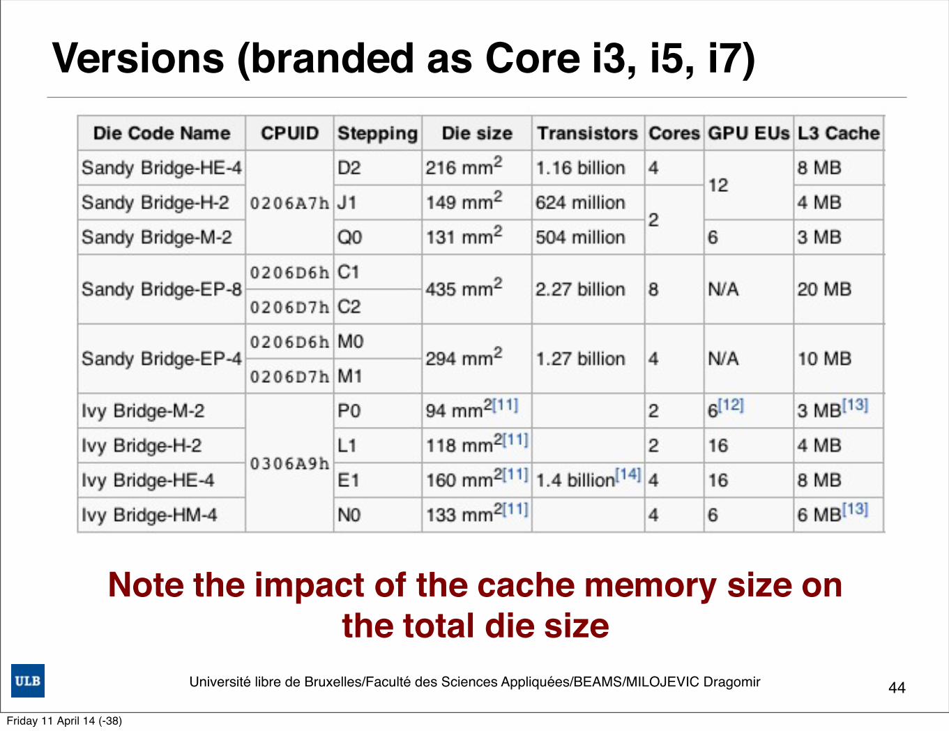
Versions (branded as Core i3, i5, i7)
44
Note the impact of the cache memory size onthe total die size
Friday 11 April 14 (-38)
Université libre de Bruxelles/Faculté des Sciences Appliquées/BEAMS/MILOJEVIC Dragomir
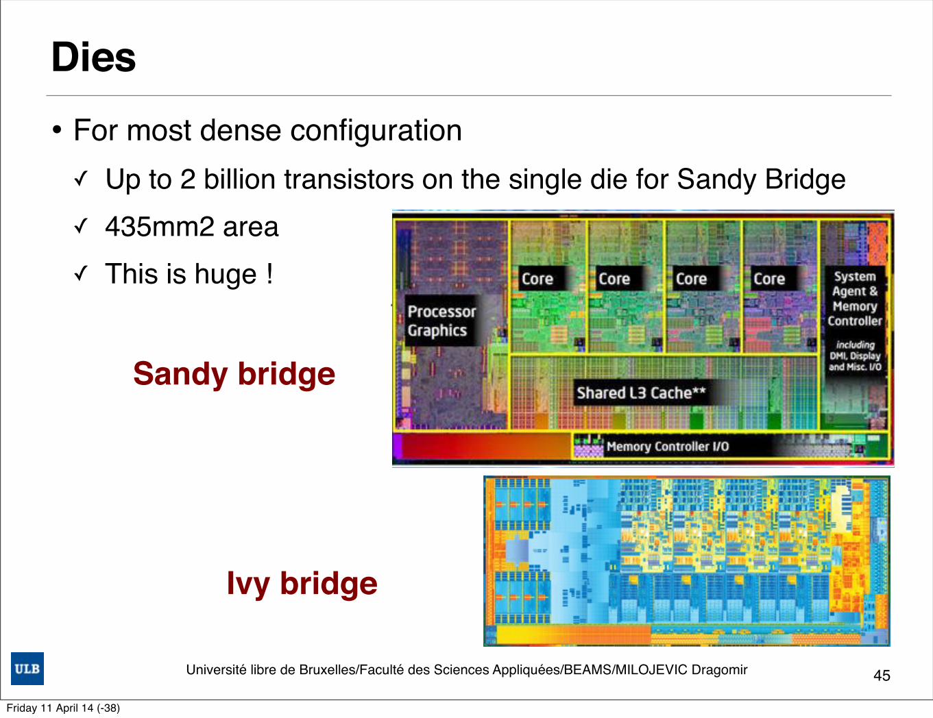
Dies• For most dense configuration ✓ Up to 2 billion transistors on the single die for Sandy Bridge✓ 435mm2 area ✓ This is huge !
45
Sandy Bridge 995 million transistors in a 216 m^2
Memory controller, the PCI Express (PCIe) controller, and video functions are all located within the processor die
Features• Uop Micro-operation Cache• Improved Branch Prediction • Advanced Vector Extensions (AVX)• The last level cache (LLC)• The System Agent• Turbo Boost• Quick Sync
Sandy bridge
Ivy bridge
Friday 11 April 14 (-38)
SandyBridge :core architecture
Friday 11 April 14 (-38)
Université libre de Bruxelles/Faculté des Sciences Appliquées/BEAMS/MILOJEVIC Dragomir
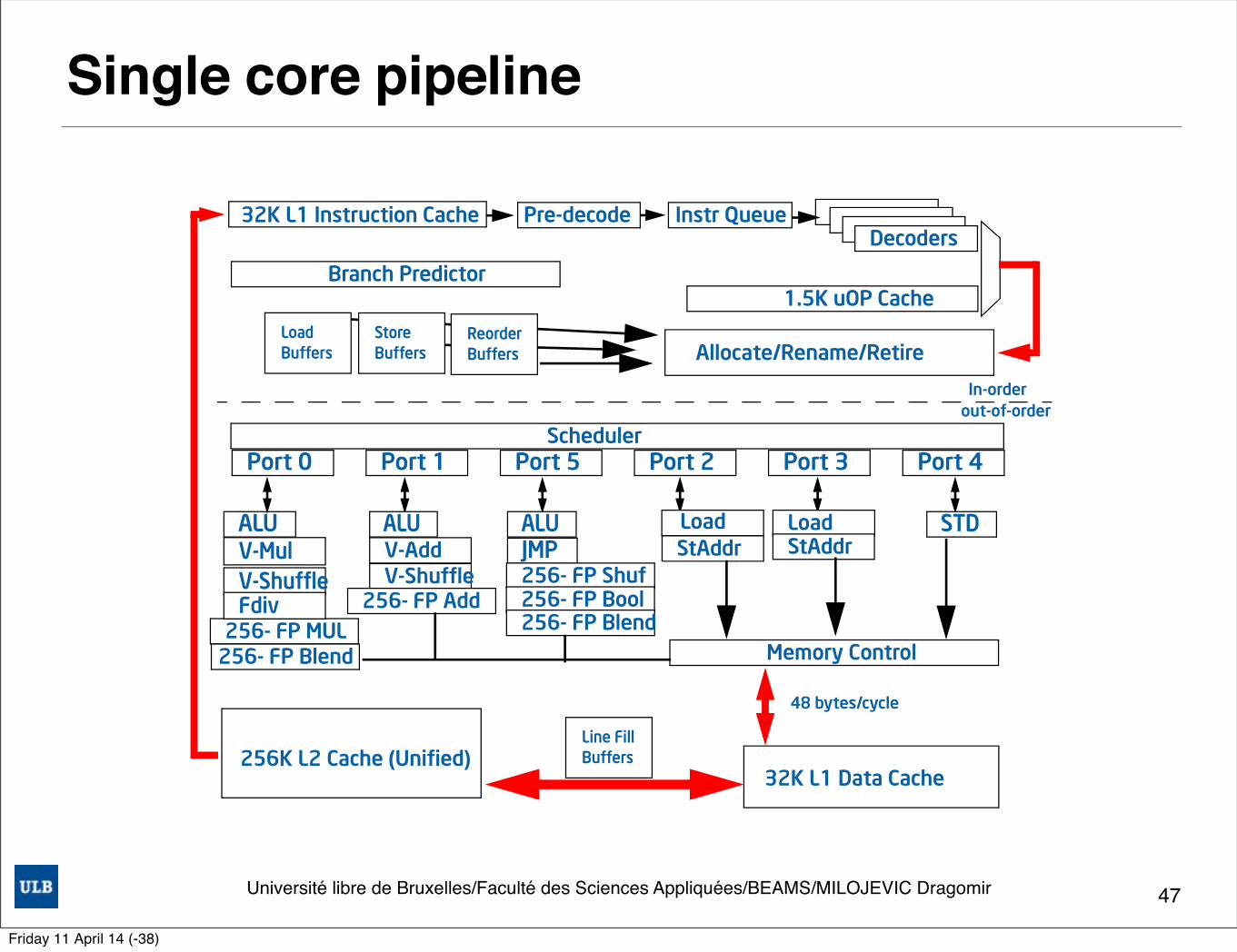
Single core pipeline
47
2-4
INTEL® 64 AND IA-32 PROCESSOR ARCHITECTURES
b. Instruction Cache, via activating the legacy decode pipeline
c. L2 cache, last level cache (LLC) and memory, as necessary
2. The micro-ops corresponding to this code are sent to the Rename/retirement block. They enter into the scheduler in program order, but execute and are de-allocated from the scheduler according to data-flow order. For simultaneously ready micro-ops, FIFO ordering is nearly always maintained. Micro-op execution is executed using execution resources arranged in threestacks. The execution units in each stack are associated with the data type ofthe instruction. Branch mispredictions are signaled at branch execution. It re-steers the frontend which delivers micro-ops from the correct path. The processor can overlapwork preceding the branch misprediction with work from the following correctedpath.
Figure 2-1. Intel microarchitecture code name Sandy Bridge Pipeline Functionality
Port 0 Port 1 Port 5 Port 2 Port 3 Port 4
256- FP MUL
ALU
V-Shuffle
Scheduler
ALU ALUJMPV-AddV-Mul
FdivV-Shuffle
Load Load STDStAddr StAddr
256- FP Add256- FP Shuf
256- FP Blend
256- FP Bool
Memory Control
32K L1 Data Cache
Allocate/Rename/Retire
Branch Predictor1.5K uOP Cache
256K L2 Cache (Unified)
32K L1 Instruction Cache Pre-decodeDecoders
Instr Queue
256- FP Blend
LoadBuffers
StoreBuffers
ReorderBuffers
Line FillBuffers
In-orderout-of-order
48 bytes/cycle
Friday 11 April 14 (-38)
Université libre de Bruxelles/Faculté des Sciences Appliquées/BEAMS/MILOJEVIC Dragomir
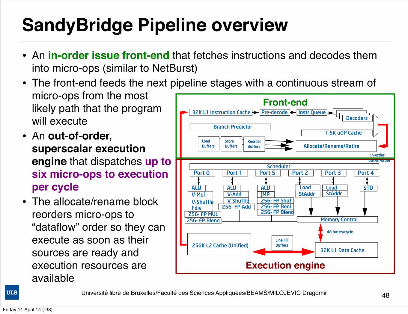
SandyBridge Pipeline overview• An in-order issue front-end that fetches instructions and decodes them
into micro-ops (similar to NetBurst) • The front-end feeds the next pipeline stages with a continuous stream of
micro-ops from the most likely path that the program will execute
• An out-of-order, superscalar execution engine that dispatches up to six micro-ops to execution per cycle
• The allocate/rename block reorders micro-ops to “dataflow” order so they can execute as soon as their sources are ready and execution resources areavailable
48
2-4
INTEL® 64 AND IA-32 PROCESSOR ARCHITECTURES
b. Instruction Cache, via activating the legacy decode pipeline
c. L2 cache, last level cache (LLC) and memory, as necessary
2. The micro-ops corresponding to this code are sent to the Rename/retirement block. They enter into the scheduler in program order, but execute and are de-allocated from the scheduler according to data-flow order. For simultaneously ready micro-ops, FIFO ordering is nearly always maintained. Micro-op execution is executed using execution resources arranged in threestacks. The execution units in each stack are associated with the data type ofthe instruction. Branch mispredictions are signaled at branch execution. It re-steers the frontend which delivers micro-ops from the correct path. The processor can overlapwork preceding the branch misprediction with work from the following correctedpath.
Figure 2-1. Intel microarchitecture code name Sandy Bridge Pipeline Functionality
Port 0 Port 1 Port 5 Port 2 Port 3 Port 4
256- FP MUL
ALU
V-Shuffle
Scheduler
ALU ALUJMPV-AddV-Mul
FdivV-Shuffle
Load Load STDStAddr StAddr
256- FP Add256- FP Shuf
256- FP Blend
256- FP Bool
Memory Control
32K L1 Data Cache
Allocate/Rename/Retire
Branch Predictor1.5K uOP Cache
256K L2 Cache (Unified)
32K L1 Instruction Cache Pre-decodeDecoders
Instr Queue
256- FP Blend
LoadBuffers
StoreBuffers
ReorderBuffers
Line FillBuffers
In-orderout-of-order
48 bytes/cycle
Front-end
Execution engine
Friday 11 April 14 (-38)
Université libre de Bruxelles/Faculté des Sciences Appliquées/BEAMS/MILOJEVIC Dragomir
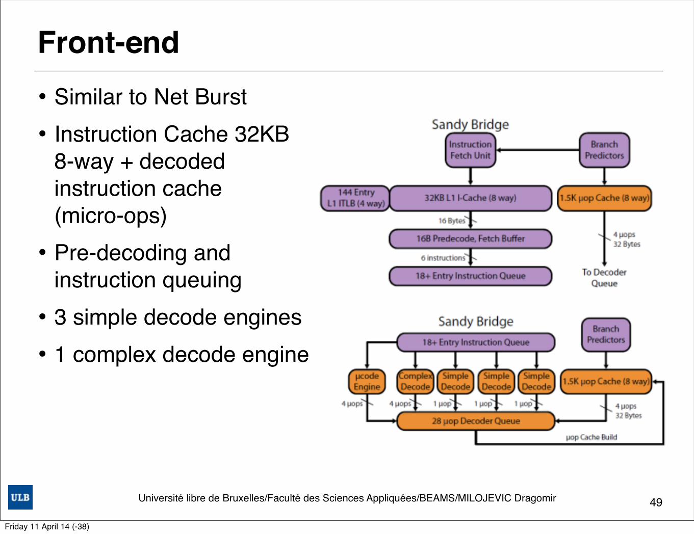
Front-end• Similar to Net Burst• Instruction Cache 32KB
8-way + decoded instruction cache (micro-ops)
• Pre-decoding and instruction queuing
• 3 simple decode engines• 1 complex decode engine
49
8/05/2012'
9'
15.32'Intel'SandyBridge'Architecture'� Improved)Nehalem)microarchitecture)
� 2<8'cores'� 1.5K'uops'cache'in'front'end'(analogy'to'trace'cache),'80%'hit'rate'� Physical'register'file.'It'does'not'store'operands'in'ROB'(eliminate'data'movements)'� Cache'broken'into'slices,'connected'with'a'ring'bus'� Introduces'AVX'instructions'(256b'SIMD)'
� PCI4Express)2.0)on)the)die)� 32'lines,'8GB'per'line'
� Intel)GPU)integrated)on)the)die)� The'GPU'shares'L3'cache'� High'performance'Video'decoder'and'encoder'
� Integrated)Memory)controller)� Up'o'4'channels'DDR3'1600MHz'
� Inter)Turbo)Technology)2.0)� Multi'step'frequency'scaling'based'on'actual'power'consumption'� Uses'accumulated'budget'(when'the'cooler'is'cold,'go'beyond'TDP'limit)'� Can'clock'down'the'GPU'and'clock'up'the'CPU'for'CPU'intensive'task'and'vice'versa'
))
_________________COMP3320)Lecture)15432)Copyright)©)2012)The)Australian)National)University_______________)
15.33'Sandy'Bridge'Organization'
_________________COMP3320)Lecture)15433)Copyright)©)2012)The)Australian)National)University_______________)
15.34'Sandy'Bridge'Front<end'
_________________COMP3320)Lecture)15434)Copyright)©)2012)The)Australian)National)University_______________)
15.35'������������� ���Dispatch'
_________________COMP3320)Lecture)15435)Copyright)©)2012)The)Australian)National)University_______________)
Friday 11 April 14 (-38)
Université libre de Bruxelles/Faculté des Sciences Appliquées/BEAMS/MILOJEVIC Dragomir
Front-end functionality • Legacy DecodePipeline✓ Decode instructions to micro-ops, delivered to the micro-op queue and
the Decoded ICache✓ Provides the same decode latency and bandwidth as prior Intel
processors• Decoded ICache✓ Provide stream of micro-ops to the micro-op queue• MSROM✓ Complex instruction micro-op, accessible from both Legacy Decode
Pipeline and Decoded ICache• Branch Prediction Unit (BPU)✓ Determine next block of code to be executed and drive lookup of
Decoded ICache and legacy decode pipelines• Micro-op queue✓ Queues micro-ops from the Decoded ICache and the legacy
decode pipeline50
Friday 11 April 14 (-38)
Université libre de Bruxelles/Faculté des Sciences Appliquées/BEAMS/MILOJEVIC Dragomir
Out-of-order engine• Improve ILP by detecting dependency chains and by executing them
out-of-of order while maintaining the correct data flow• When a dependency chain is waiting for a resource, such as a
second-level data cache line, it sends micro-ops from another chain to the execution core
• Designed with power savings in mind too !• Components :✓ Renamer — moves micro-ops from the front-end to the execution core;
eliminates false dependencies among micro-ops, thereby enabling out-of-order execution of micro-ops
✓ Schedule — queues micro-ops until all source operands are ready; schedules and dispatches ready micro-ops to the available execution units in as close to a first in first out (FIFO) order as possible
✓ Retirement — retires instructions and micro-ops in order and handles faults and exceptions
51
Friday 11 April 14 (-38)
Université libre de Bruxelles/Faculté des Sciences Appliquées/BEAMS/MILOJEVIC Dragomir
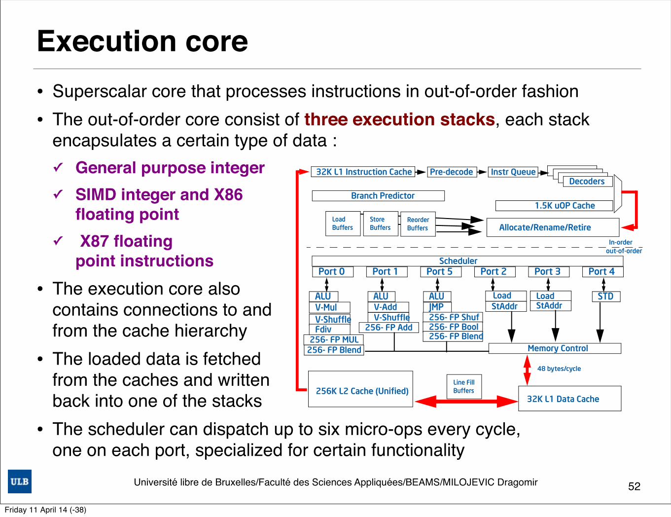
Execution core• Superscalar core that processes instructions in out-of-order fashion• The out-of-order core consist of three execution stacks, each stack
encapsulates a certain type of data : ✓ General purpose integer✓ SIMD integer and X86
floating point✓ X87 floating
point instructions
• The execution core also contains connections to and from the cache hierarchy
• The loaded data is fetched from the caches and written back into one of the stacks
• The scheduler can dispatch up to six micro-ops every cycle, one on each port, specialized for certain functionality
52
2-4
INTEL® 64 AND IA-32 PROCESSOR ARCHITECTURES
b. Instruction Cache, via activating the legacy decode pipeline
c. L2 cache, last level cache (LLC) and memory, as necessary
2. The micro-ops corresponding to this code are sent to the Rename/retirement block. They enter into the scheduler in program order, but execute and are de-allocated from the scheduler according to data-flow order. For simultaneously ready micro-ops, FIFO ordering is nearly always maintained. Micro-op execution is executed using execution resources arranged in threestacks. The execution units in each stack are associated with the data type ofthe instruction. Branch mispredictions are signaled at branch execution. It re-steers the frontend which delivers micro-ops from the correct path. The processor can overlapwork preceding the branch misprediction with work from the following correctedpath.
Figure 2-1. Intel microarchitecture code name Sandy Bridge Pipeline Functionality
Port 0 Port 1 Port 5 Port 2 Port 3 Port 4
256- FP MUL
ALU
V-Shuffle
Scheduler
ALU ALUJMPV-AddV-Mul
FdivV-Shuffle
Load Load STDStAddr StAddr
256- FP Add256- FP Shuf
256- FP Blend
256- FP Bool
Memory Control
32K L1 Data Cache
Allocate/Rename/Retire
Branch Predictor1.5K uOP Cache
256K L2 Cache (Unified)
32K L1 Instruction Cache Pre-decodeDecoders
Instr Queue
256- FP Blend
LoadBuffers
StoreBuffers
ReorderBuffers
Line FillBuffers
In-orderout-of-order
48 bytes/cycle
Friday 11 April 14 (-38)
Université libre de Bruxelles/Faculté des Sciences Appliquées/BEAMS/MILOJEVIC Dragomir
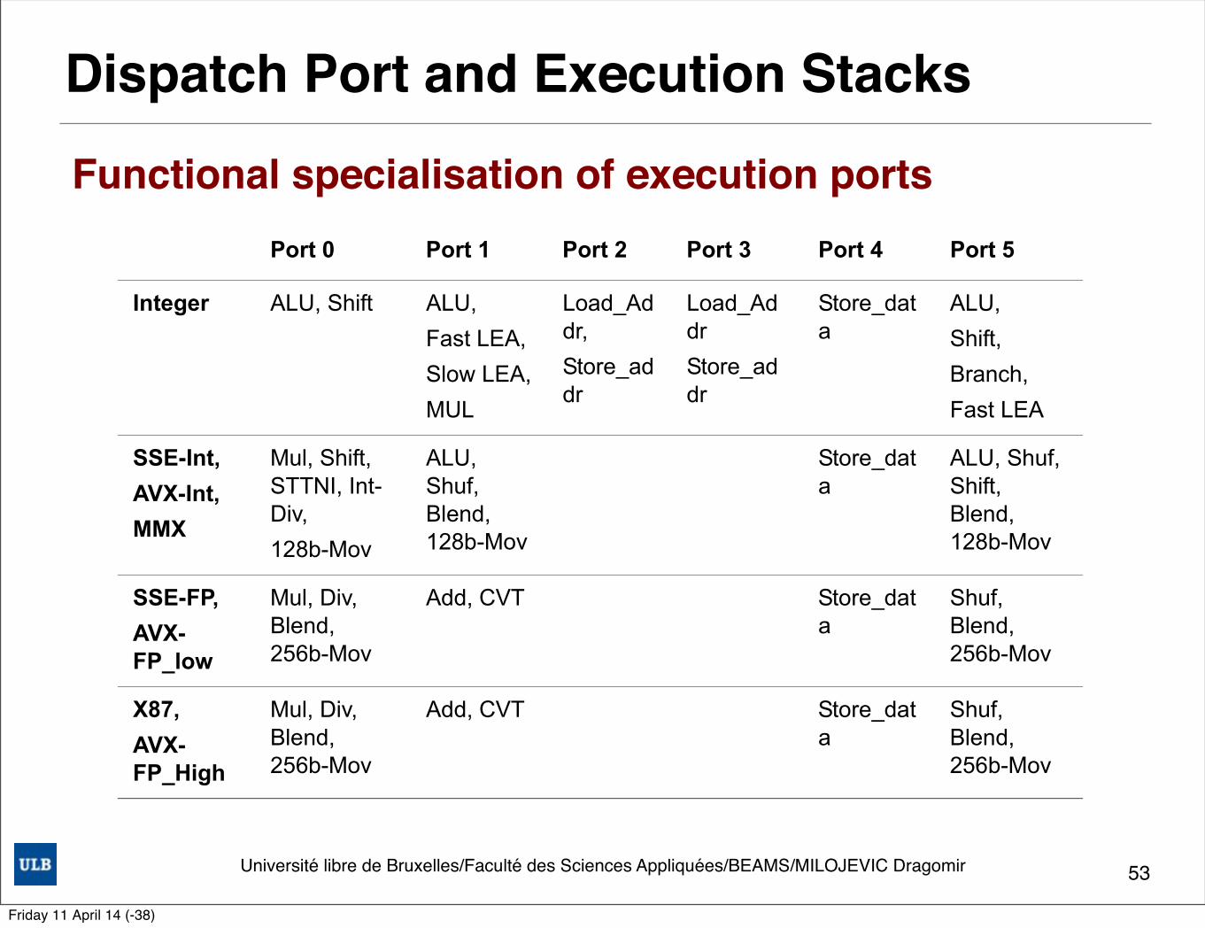
Dispatch Port and Execution Stacks
53
2-14
INTEL® 64 AND IA-32 PROCESSOR ARCHITECTURES
! General purpose integer ! SIMD integer and floating point! X87
The execution core also contains connections to and from the cache hierarchy. The loaded data is fetched from the caches and written back into one of the stacks.
The scheduler can dispatch up to six micro-ops every cycle, one on each port. The following table summarizes which operations can be dispatched on which port.
After execution, the data is written back on a writeback bus corresponding to the dispatch port and the data type of the result. Micro-ops that are dispatched on the same port but have different latencies may need the write back bus at the same cycle. In these cases the execution of one of the micro-ops is delayed until the write-back bus is available. For example, MULPS (five cycles) and BLENDPS (one cycle) may collide if both are ready for execution on port 0: first the MULPS and four cycles later the BLENDPS. Intel microarchitecture code name Sandy Bridge eliminates such collisions as long as the micro-ops write the results to different stacks. For example, integer ADD (one cycle) can be dispatched four cycles after MULPS (five cycles) since the integer ADD uses the integer stack while the MULPS uses the FP stack.
When a source of a micro-op executed in one stack comes from a micro-op executed in another stack, a one- or two-cycle delay can occur. The delay occurs also for tran-sitions between Intel SSE integer and Intel SSE floating-point operations. In some of
Table 2-3. Dispatch Port and Execution Stacks
Port 0 Port 1 Port 2 Port 3 Port 4 Port 5
Integer ALU, Shift ALU,Fast LEA,Slow LEA,MUL
Load_Addr,Store_addr
Load_AddrStore_addr
Store_data
ALU,Shift,Branch,Fast LEA
SSE-Int,AVX-Int,MMX
Mul, Shift, STTNI, Int-Div,128b-Mov
ALU, Shuf, Blend, 128b-Mov
Store_data
ALU, Shuf, Shift, Blend, 128b-Mov
SSE-FP,AVX-FP_low
Mul, Div, Blend, 256b-Mov
Add, CVT Store_data
Shuf, Blend, 256b-Mov
X87,AVX-FP_High
Mul, Div, Blend, 256b-Mov
Add, CVT Store_data
Shuf, Blend, 256b-Mov
Functional specialisation of execution ports
Friday 11 April 14 (-38)
Université libre de Bruxelles/Faculté des Sciences Appliquées/BEAMS/MILOJEVIC Dragomir
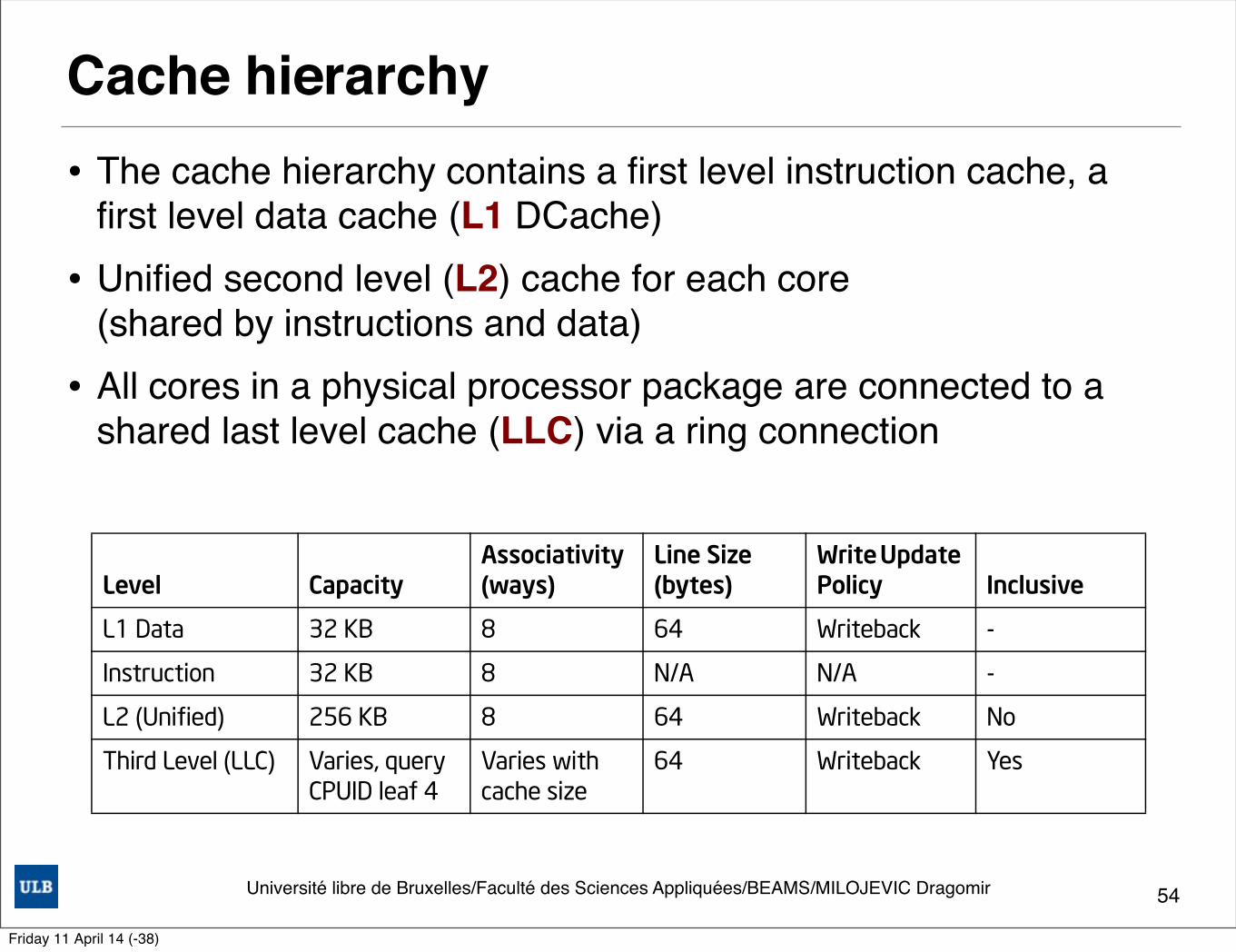
Cache hierarchy• The cache hierarchy contains a first level instruction cache, a
first level data cache (L1 DCache) • Unified second level (L2) cache for each core
(shared by instructions and data)• All cores in a physical processor package are connected to a
shared last level cache (LLC) via a ring connection
54
2-16
INTEL® 64 AND IA-32 PROCESSOR ARCHITECTURES
2.1.5.1 Load and Store Operation Overview
This section provides an overview of the load and store operations.
Loads
When an instruction reads data from a memory location that has write-back (WB) type, the processor looks for it in the caches and memory. Table 2-6 shows the access lookup order and best case latency. The actual latency can vary depending on the cache queue occupancy, LLC ring occupancy, memory components, and their parameters.
The LLC is inclusive of all cache levels above it - data contained in the core caches must also reside in the LLC. Each cache line in the LLC holds an indication of the cores that may have this line in their L2 and L1 caches. If there is an indication in the LLC that other cores may hold the line of interest and its state might have to modify, there is a lookup into the L1 DCache and L2 of these cores too. The lookup is called "clean" if it does not require fetching data from the other core caches. The lookup is
Table 2-5. Cache Parameters
Level CapacityAssociativity (ways)
Line Size (bytes)
Write Update Policy Inclusive
L1 Data 32 KB 8 64 Writeback -
Instruction 32 KB 8 N/A N/A -
L2 (Unified) 256 KB 8 64 Writeback No
Third Level (LLC) Varies, query CPUID leaf 4
Varies with cache size
64 Writeback Yes
Table 2-6. Lookup Order and Load Latency
Level Latency (cycles) Bandwidth (per core per cycle)
L1 Data 41
NOTES:1. Subject to execution core bypass restriction shown in Table 2-4.
2 x16 bytes
L2 (Unified) 12 1 x 32 bytes
Third Level (LLC) 26-312
2. Latency of L3 varies with product segment and sku. The values apply to second generation IntelCore processor families.
1 x 32 bytes
L2 and L1 DCache in other cores if applicable
43- clean hit;
60 - dirty hit
Friday 11 April 14 (-38)
Université libre de Bruxelles/Faculté des Sciences Appliquées/BEAMS/MILOJEVIC Dragomir
Cache hierarchy• L1 is private to a core • L1D cache may be shared by two logical processors if the
processor support HyperThreading • The L2 cache is shared by instructions and data• The caches use the services of the ✓ Instruction Translation Lookaside Buffer (ITLB), ✓ Data Translation Lookaside Buffer (DTLB) and ✓ Shared Translation Lookaside Buffer (STLB)
• These are used to translate linear addresses to physical address
• Data coherency in all cache levels is maintained using the MESI protocol
55
Friday 11 April 14 (-38)
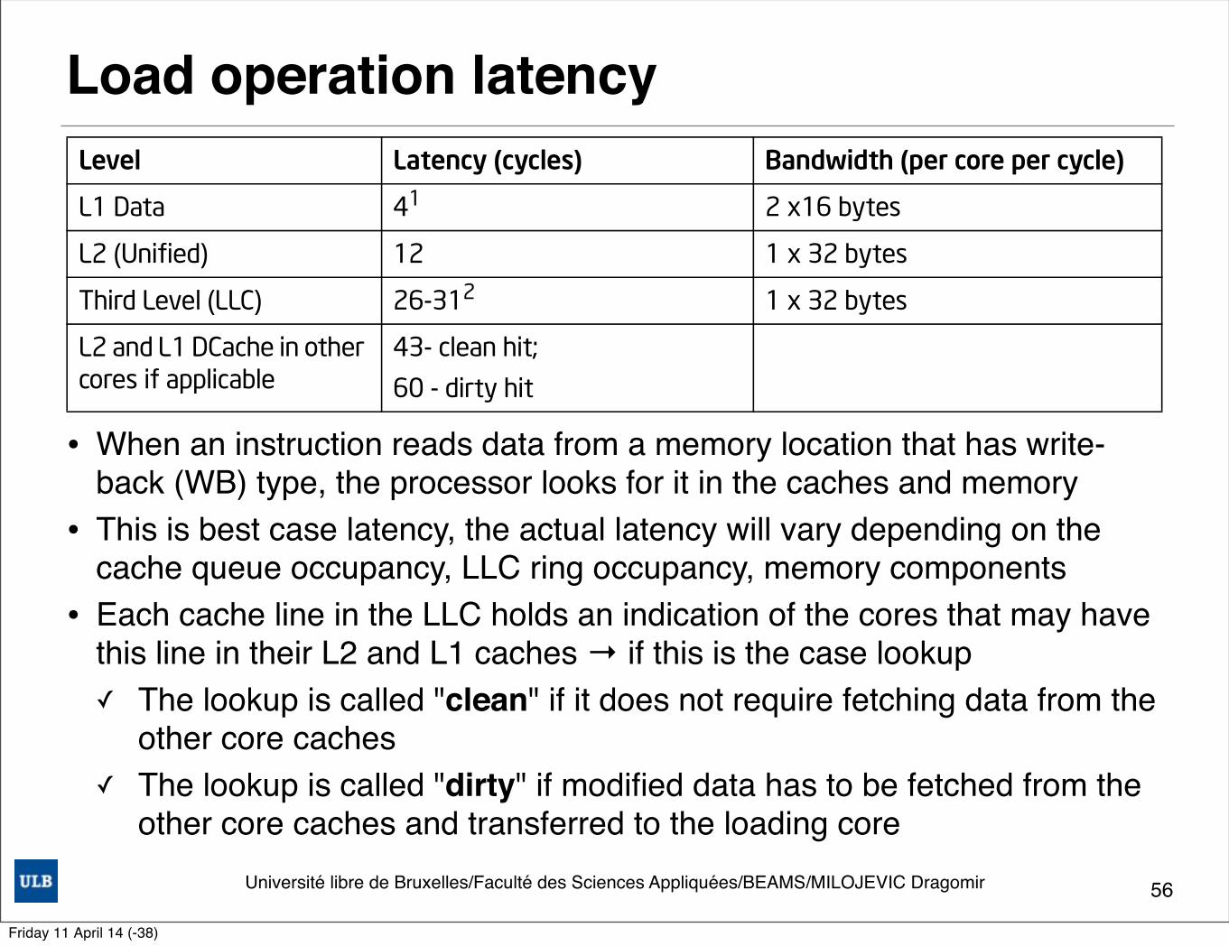
Université libre de Bruxelles/Faculté des Sciences Appliquées/BEAMS/MILOJEVIC Dragomir
Load operation latency
• When an instruction reads data from a memory location that has write-back (WB) type, the processor looks for it in the caches and memory
• This is best case latency, the actual latency will vary depending on the cache queue occupancy, LLC ring occupancy, memory components
• Each cache line in the LLC holds an indication of the cores that may have this line in their L2 and L1 caches → if this is the case lookup ✓ The lookup is called "clean" if it does not require fetching data from the
other core caches✓ The lookup is called "dirty" if modified data has to be fetched from the
other core caches and transferred to the loading core
56
2-16
INTEL® 64 AND IA-32 PROCESSOR ARCHITECTURES
2.1.5.1 Load and Store Operation Overview
This section provides an overview of the load and store operations.
Loads
When an instruction reads data from a memory location that has write-back (WB) type, the processor looks for it in the caches and memory. Table 2-6 shows the access lookup order and best case latency. The actual latency can vary depending on the cache queue occupancy, LLC ring occupancy, memory components, and their parameters.
The LLC is inclusive of all cache levels above it - data contained in the core caches must also reside in the LLC. Each cache line in the LLC holds an indication of the cores that may have this line in their L2 and L1 caches. If there is an indication in the LLC that other cores may hold the line of interest and its state might have to modify, there is a lookup into the L1 DCache and L2 of these cores too. The lookup is called "clean" if it does not require fetching data from the other core caches. The lookup is
Table 2-5. Cache Parameters
Level CapacityAssociativity (ways)
Line Size (bytes)
Write Update Policy Inclusive
L1 Data 32 KB 8 64 Writeback -
Instruction 32 KB 8 N/A N/A -
L2 (Unified) 256 KB 8 64 Writeback No
Third Level (LLC) Varies, query CPUID leaf 4
Varies with cache size
64 Writeback Yes
Table 2-6. Lookup Order and Load Latency
Level Latency (cycles) Bandwidth (per core per cycle)
L1 Data 41
NOTES:1. Subject to execution core bypass restriction shown in Table 2-4.
2 x16 bytes
L2 (Unified) 12 1 x 32 bytes
Third Level (LLC) 26-312
2. Latency of L3 varies with product segment and sku. The values apply to second generation IntelCore processor families.
1 x 32 bytes
L2 and L1 DCache in other cores if applicable
43- clean hit;
60 - dirty hit
Friday 11 April 14 (-38)
Université libre de Bruxelles/Faculté des Sciences Appliquées/BEAMS/MILOJEVIC Dragomir
Store• When an instruction writes data to a memory that has a write back
memory type, the processor first ensures that it has the line containing this memory location in its L1 DCache
• If the cache line is not there (and in the right coherency state), the processor fetches it from the next levels of the memory hierarchy using a Read for Ownership request in the specified order:✓ L1 DCache✓ L2✓ Last Level Cache✓ L2 and L1 DCache in other cores, if applicable✓ Memory
• Once the cache line is in the L1 DCache, the new data is written to it, and the line is marked as Modified state
• Low latency cost, except if multiple consecutive write cache misses
57
Friday 11 April 14 (-38)

Université libre de Bruxelles/Faculté des Sciences Appliquées/BEAMS/MILOJEVIC Dragomir
SIMD• Legacy : from MMX to SSE4.2 + AVX• AVX✓ Support for 256-bit wide vectors and 16 SIMD register set✓ 256-bit floating-point instruction set enhancement with up to 2X
performance gain relative to 128-bit Streaming SIMD extensions.✓ Instruction syntax support for generalized three-operand syntax
to improve instruction programming flexibility and efficient encoding of new instruction extensions
✓ Enhancement of legacy 128-bit SIMD instruction extensions to support three-operand syntax and to simplify compiler vectorization of high-level language expressions.
✓ Support flexible deployment of 256-bit AVX code, 128-bit AVX code, legacy 128- bit code and scalar code
58
Friday 11 April 14 (-38)
Power and thermal management
Friday 11 April 14 (-38)
Université libre de Bruxelles/Faculté des Sciences Appliquées/BEAMS/MILOJEVIC Dragomir
Power in ICs• Power is a problem in current ICs : limited frequency speed-ups
from node to node because of the power and associated thermal • Has two components ✓ Dynamic — when gates are toggling (output of the gates changes
due to input changes)✓ Static — due to leakage, transistors are not perfect switches
• While in the past dynamic component has been pre-dominant, over the years static power dissipation became as important
• To deal with static power dissipation we need to “cut” the✓ clock supply — clock gating or reduce clock period ✓ Vdd — power gating
• Most of the ICs implement these techniques; for general purpose CPU it is important to have an interface with the layers above
60
Friday 11 April 14 (-38)
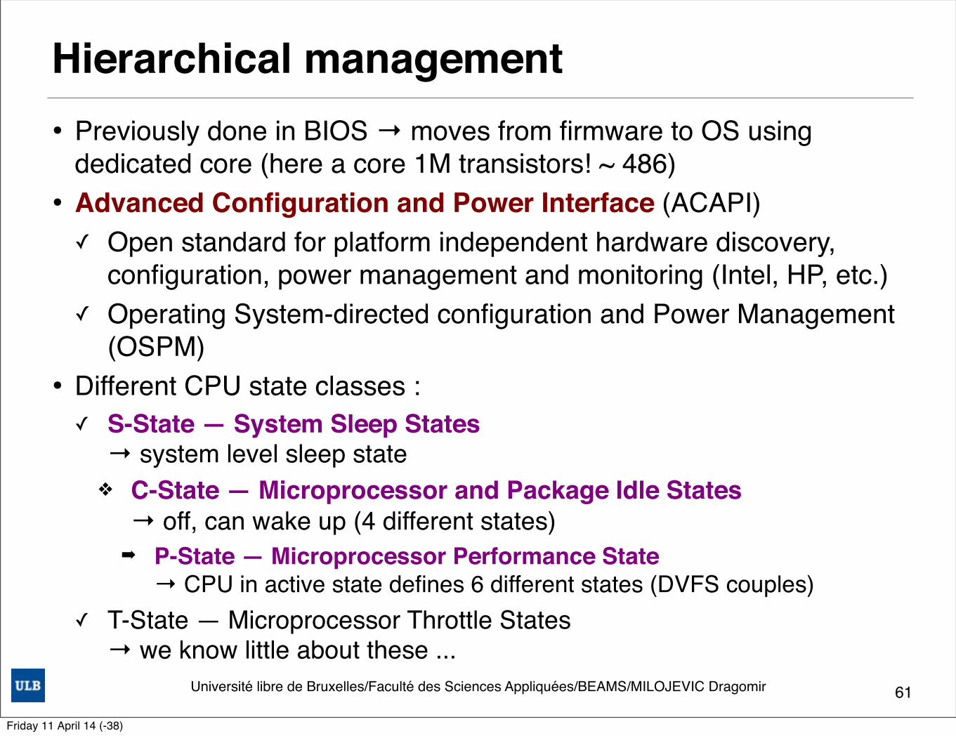
Université libre de Bruxelles/Faculté des Sciences Appliquées/BEAMS/MILOJEVIC Dragomir
Hierarchical management• Previously done in BIOS → moves from firmware to OS using
dedicated core (here a core 1M transistors! ~ 486)• Advanced Configuration and Power Interface (ACAPI)✓ Open standard for platform independent hardware discovery,
configuration, power management and monitoring (Intel, HP, etc.)✓ Operating System-directed configuration and Power Management
(OSPM)• Different CPU state classes : ✓ S-State — System Sleep States→ system level sleep state❖ C-State — Microprocessor and Package Idle States→ off, can wake up (4 different states)
➡ P-State — Microprocessor Performance State → CPU in active state defines 6 different states (DVFS couples)
✓ T-State — Microprocessor Throttle States→ we know little about these ...
61
Friday 11 April 14 (-38)

Université libre de Bruxelles/Faculté des Sciences Appliquées/BEAMS/MILOJEVIC Dragomir
S-States — System Sleep States
62
S0
S1
S2
S3
S5
ShutDown
S4
HibernationState is saved on HDD, practically no power dissipation
CPU + chipset is off but DRAM remains powered-up and contains the saved execution context
System is active : any P or C-state
CPU is off, the execution context is saved in DRAM
Time to wake-up increases but the power goes down
Minimumlive state
Friday 11 April 14 (-38)
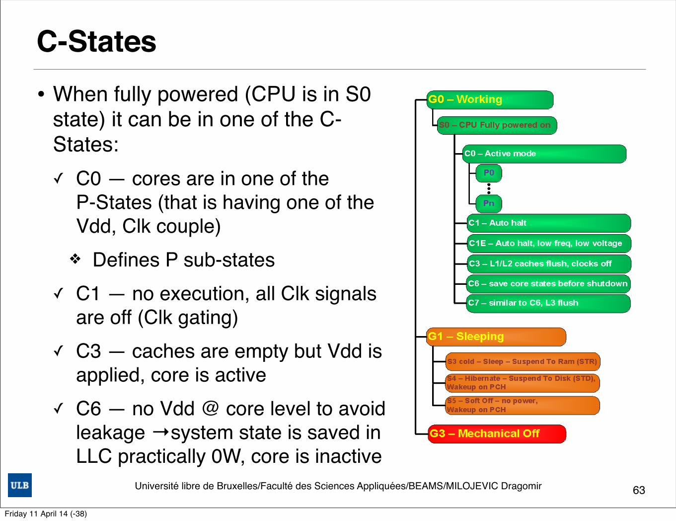
Université libre de Bruxelles/Faculté des Sciences Appliquées/BEAMS/MILOJEVIC Dragomir
C-States• When fully powered (CPU is in S0
state) it can be in one of the C-States:✓ C0 — cores are in one of the
P-States (that is having one of the Vdd, Clk couple)❖ Defines P sub-states
✓ C1 — no execution, all Clk signals are off (Clk gating)
✓ C3 — caches are empty but Vdd is applied, core is active
✓ C6 — no Vdd @ core level to avoid leakage →system state is saved in LLC practically 0W, core is inactive
63
Datasheet, Volume 1 43
Power Management
4 Power Management
This chapter provides information on the following power management topics:
= Advanced Configuration and Power Interface (ACPI) States= Processor Core= Integrated Memory Controller (IMC)= PCI Express*= Direct Media Interface (DMI)= Processor Graphics Controller
Figure 4-1. Power States
Friday 11 April 14 (-38)
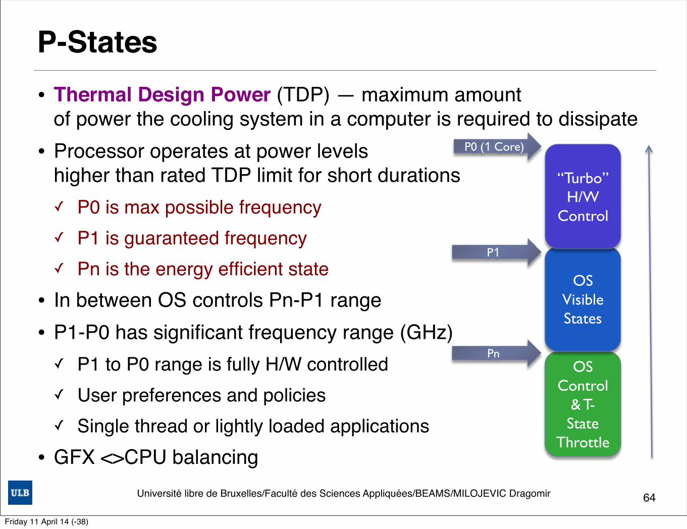
Université libre de Bruxelles/Faculté des Sciences Appliquées/BEAMS/MILOJEVIC Dragomir
P-States• Thermal Design Power (TDP) — maximum amount
of power the cooling system in a computer is required to dissipate• Processor operates at power levels
higher than rated TDP limit for short durations✓ P0 is max possible frequency✓ P1 is guaranteed frequency✓ Pn is the energy efficient state
• In between OS controls Pn-P1 range• P1-P0 has significant frequency range (GHz) ✓ P1 to P0 range is fully H/W controlled ✓ User preferences and policies✓ Single thread or lightly loaded applications
• GFX <>CPU balancing
64
Intel® Turbo,Boost,Technology,2.0
14
� Performance on Demand
� CPU can run faster than base operating frequency
� Working within power, current and temperature constraints
� Dependent on number of active cores
� Highest frequency is with 1 core (gets all the headroom)
� Processor operates at power level higher than rated upper power limit (TDP) for short durations
� P0 is Maximum Possible Frequency
� P1 is Guaranteed Frequency
� Pn is Energy Efficient Frequency
OS
Control
& T-
State
Throttle
OS
Visible
States
“Turbo”
H/W
Control
Frequency
Pn
P1
P0 (1 Core)
Friday 11 April 14 (-38)
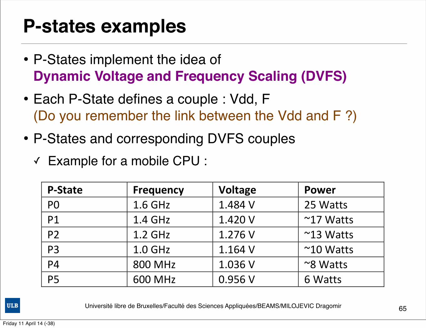
Université libre de Bruxelles/Faculté des Sciences Appliquées/BEAMS/MILOJEVIC Dragomir
P-states examples• P-States implement the idea of
Dynamic Voltage and Frequency Scaling (DVFS)• Each P-State defines a couple : Vdd, F
(Do you remember the link between the Vdd and F ?)• P-States and corresponding DVFS couples ✓ Example for a mobile CPU :
65
Friday 11 April 14 (-38)
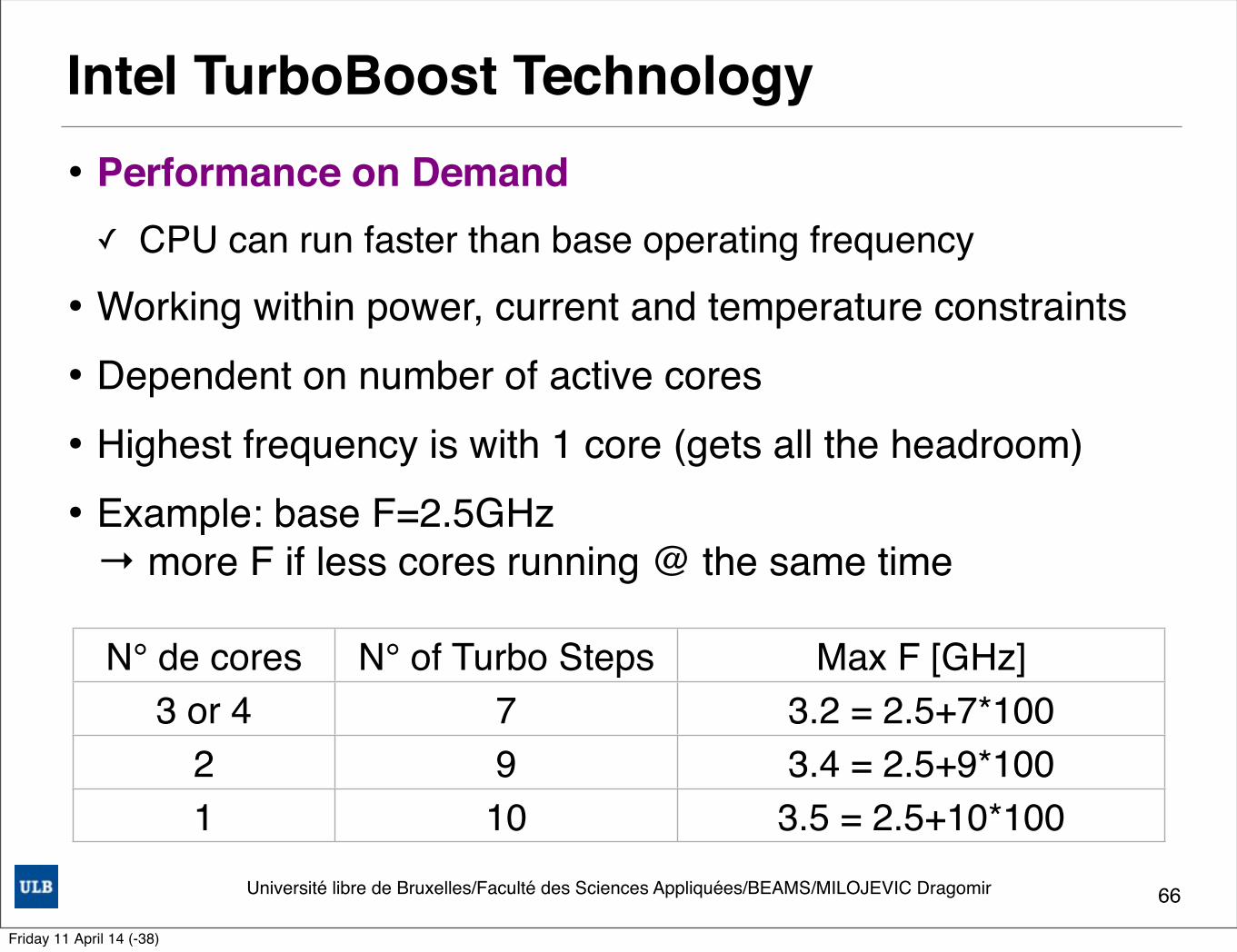
Université libre de Bruxelles/Faculté des Sciences Appliquées/BEAMS/MILOJEVIC Dragomir
Intel TurboBoost Technology• Performance on Demand ✓ CPU can run faster than base operating frequency
• Working within power, current and temperature constraints
• Dependent on number of active cores
• Highest frequency is with 1 core (gets all the headroom)
• Example: base F=2.5GHz → more F if less cores running @ the same time
66
N° de cores N° of Turbo Steps Max F [GHz]3 or 4 7 3.2 = 2.5+7*100
2 9 3.4 = 2.5+9*1001 10 3.5 = 2.5+10*100
Friday 11 April 14 (-38)
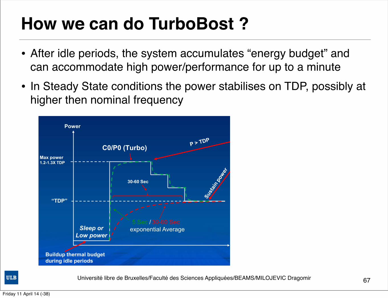
Université libre de Bruxelles/Faculté des Sciences Appliquées/BEAMS/MILOJEVIC Dragomir
How we can do TurboBost ?• After idle periods, the system accumulates “energy budget” and
can accommodate high power/performance for up to a minute
• In Steady State conditions the power stabilises on TDP, possibly at higher then nominal frequency
6714Sandy Bridge - Hot Chips 2011
C0/P0 (Turbo)
After idle periods, the system accumulates “energy budget” and can accommodate high power/performance for up to a minute
Use accumulated energy budget to
enhance user experience
Intel® Turbo Boost Technology 2.0 - Dynamic
Time
Power
Sleep orLow power
“TDP”
Buildup thermal budget during idle periods
Max power1.2-1.3X TDP
30-60 Sec exponential Average5 Sec /
30-60 Sec
In Steady State conditions the power stabilizes on TDP, possibly at higher then nominal frequency
Friday 11 April 14 (-38)
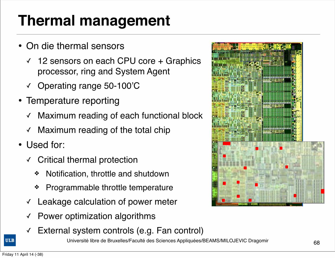
Université libre de Bruxelles/Faculté des Sciences Appliquées/BEAMS/MILOJEVIC Dragomir
Thermal management• On die thermal sensors✓ 12 sensors on each CPU core + Graphics
processor, ring and System Agent ✓ Operating range 50-100’C
• Temperature reporting✓ Maximum reading of each functional block✓ Maximum reading of the total chip
• Used for:✓ Critical thermal protection
❖ Notification, throttle and shutdown❖ Programmable throttle temperature
✓ Leakage calculation of power meter ✓ Power optimization algorithms✓ External system controls (e.g. Fan control)
68
25Sandy Bridge - Hot Chips 2011
Package thermal management
� On die thermal sensors� 12 sensors on each CPU core + PG, ring and
SA� Operating range 50-100’C
� Temperature reporting � Maximum reading of each functional block and
maximum reading of the total chip� Used for:
� Critical thermal protection� Notification, throttle and shutdown� Programmable throttle temperature
� Leakage calculation of power meter� PCU optimization algorithms� External system controls (e.g. Fan control)
Friday 11 April 14 (-38)