Embed Size (px)
Citation preview
Modulation of Semiconductor
Photoluminescence with Intense
Terahertz Pulses
by
David N. Purschke
A thesis submitted in partial fulfillment of the requirements for the degree of
Master of Science
Department of Physics
University of Alberta
c©David N. Purschke, 2016

Abstract
Over the last 5 years, tilted pulse-front terahertz (THz) generation has
opened the door to new studies of nonlinear dynamics in a variety of ma-
terials. With access to strong electric fields that turn on and off over pi-
cosecond timescales exciting new possibilities exist to control light-matter
interaction. We have developed a new intense THz pulse source, with a
peak electric field of 230 kV/cm for exploring nonlinear dynamics in semi-
conductors.
Here, we study the effects of THz pulses on semiconductor photolumines-
cence (PL). When a femtosecond optical and single-cycle intense THz pulse
are simultaneously incident on a direct-gap semiconductor, the THz pulse
enhances high energy and quenches low energy PL. However, with time de-
lays larger than 1 ps, no modulation of the PL occurs.
We have systematically studied the THz-pulse-induced change in PL (THz-
∆PL) over a wide range of THz energies and photoexcitation densities in
gallium arsenide (GaAs) and indium phosphide (InP) to help understand
the mechanism. In most cases, the quenching dominates and there is inte-
grated PL quenching (PLQ). With increasing photoexcited carrier density,
the fractional quenching decreases, while the enhancement increases, and
less integrated modulation occurs. At high excitation density, by changing
ii

the temporal profile of the photoexcitation pulse, the enhancment can be
made to dominate and there is integrated PL enhancement (PLE).
The origin of this behaviour has to do with the redistribution of carriers
in phase space by the strong electric field of the THz pulse. In real space,
oppositely charged electrons and holes are spatially separated. In momen-
tum space, hot electrons scatter to satellite valleys, increasing the rise-time
of the PL, slowing carrier diffusion, and releasing a large number of high
wavevector phonons.
Despite our understanding of these processes, a precise description of the
THz-∆PL is still not completely clear. Possible explanations for these ef-
fects are discussed, including suppression of stimulated emission, enhanced
surface recombination, and non-radiative recombination involving interval-
ley phonons.
iii

Preface
I herewith declare that I have produced this paper without the prohibited
assistance of third parties and without making use of aids other than those
specified; notions taken over directly or indirectly from other sources have
been identified as such.
The thesis work was conducted from September 2014 to August 2016 under
the supervision of Frank Hegmann at the University of Alberta.

Acknowledgements
Grad school is a lot like riding a roller coaster built by a person who had no
idea what they were doing. It just sounded like fun, so they gave it a shot.
In this case, that person is you. You started building your own roller coaster
the day you decided to go to grad school. My own roller coaster has had
many ups and downs. There will be many more to come, as I begin my PhD
studies in just two weeks. What I’ve learned so far is a little bit about build-
ing roller coasters, and a lot about how important it is to have help doing it.
With that, I would like to start by thanking my supervisor, Dr. Frank
Hegmann. You’ve been there for me more times than I can count. It goes
without saying that I would not have gotten to this point without your
help and guidance. I would like to thank our former research associate, Dr.
Lyuba Titova. My first eight months in the lab were under your guidance
and I will not forget what I learned from you about both terahertz pulses,
and life.
I would like to thank my Committee members, Dr. Rick Sydora and Dr.
Joseph Maciejko, who have provided me with valuable advice. I would es-
pecially like to thank Joseph whos door has always been open when I’ve had
questions. I would like to thank Greg Popowich, and Beipei Shi for techni-
cal support. I would like to thank Dr. Frank Marsiglio, and Dr. Lindsay
LeBlanc for their helpful discussions.
I would like to thank my current and former lab mates Vedran Jelic, Mary
Narreto, Peter Ngyuen, Cameron Hough, Charles Jensen, Glenda de los
v

Reyes, Ayesheshim Ayesheshim, Zhenyou Wang, Christopher Rathje, Alexan-
der Bourgund, and William Morrish. I would especially like to thank Mary
Narreto who edited my entire thesis in one day, for which I am very grate-
ful. I would like to thank all current and former undergraduate students
who have worked with me: Andrew Longman, Ketty Na, Haille Sharum,
Christopher Mannes, Kameron Palmer, and Daniel Mildenberger. I would
also like to thank Daniel for providing the FROG trace that is in my thesis.
I would like to thank my former roommates Scott and Jenn, and my cur-
rent roommate Andrew, all of whom I leaned on for support during times
of stress. I would like to thank all of my friends who helped make me who I
am. I would like to thank my intramurals sports teams, as bad as it sounds
there is no better stress relief than hitting a layup, a spike, or tossing a
hammer for a point.
I would like to acknowledge the thousands of individuals who have coded
for the LaTeX project for free.
And finally, I would like to thank the people who I lean on the most. My
girlfriend Tatiana, who has been more supportive and understand than I
could hope for. Tata, I’m lucky to have you. My brother Andrew, and
his wife Carrie, and my grandparents, Fran, Norm, and Irene. Most of
all, I would like to thank my parents Garry and Eunice for their support.
Throughout it all, you have not only allowed me to find my own way in life,
but you have helped facilitate it. I am forever in your debt.
vi

Contents
List of Figures ix
List of Tables xi
1 Introduction 2
2 Ultrafast Excitation and Relaxation of Semiconductors 7
2.1 Semiconductor Physics . . . . . . . . . . . . . . . . . . . . . . . . . . . . 9
2.1.1 Crystal Lattice . . . . . . . . . . . . . . . . . . . . . . . . . . . . 9
2.1.2 Electronic Structure . . . . . . . . . . . . . . . . . . . . . . . . . 10
2.1.3 Phonon Dispersion . . . . . . . . . . . . . . . . . . . . . . . . . . 12
2.1.4 Thermal Excitations . . . . . . . . . . . . . . . . . . . . . . . . . 12
2.1.5 Localized States . . . . . . . . . . . . . . . . . . . . . . . . . . . 14
2.2 Dynamics . . . . . . . . . . . . . . . . . . . . . . . . . . . . . . . . . . . 15
2.2.1 Absorption of Light . . . . . . . . . . . . . . . . . . . . . . . . . 17
2.2.2 Coulomb Scattering . . . . . . . . . . . . . . . . . . . . . . . . . 18
2.2.3 Carrier-Phonon Scattering . . . . . . . . . . . . . . . . . . . . . . 20
2.2.4 Surface Effects . . . . . . . . . . . . . . . . . . . . . . . . . . . . 22
2.3 Summary . . . . . . . . . . . . . . . . . . . . . . . . . . . . . . . . . . . 23
3 Experimental Details 26
3.1 Laser System . . . . . . . . . . . . . . . . . . . . . . . . . . . . . . . . . 28
3.1.1 Oscillator . . . . . . . . . . . . . . . . . . . . . . . . . . . . . . . 28
3.1.2 Amplifier . . . . . . . . . . . . . . . . . . . . . . . . . . . . . . . 28
3.1.3 Beam Routing . . . . . . . . . . . . . . . . . . . . . . . . . . . . 32
3.2 Intense THz Source . . . . . . . . . . . . . . . . . . . . . . . . . . . . . . 33
vii

CONTENTS
3.2.1 Pulse Front Tilting Optics . . . . . . . . . . . . . . . . . . . . . . 35
3.2.2 THz Routing Optics . . . . . . . . . . . . . . . . . . . . . . . . . 37
3.2.3 Electro-Optic Sampling Setup . . . . . . . . . . . . . . . . . . . . 37
3.2.4 Source Alignment . . . . . . . . . . . . . . . . . . . . . . . . . . 38
3.2.5 Source Characterization . . . . . . . . . . . . . . . . . . . . . . . 41
3.3 THz Modulation of PL Experimental Layout . . . . . . . . . . . . . . . 44
4 THz Modulation of Photoluminescence 48
4.1 Sample Details . . . . . . . . . . . . . . . . . . . . . . . . . . . . . . . . 50
4.2 THz-∆L in GaAs . . . . . . . . . . . . . . . . . . . . . . . . . . . . . . . 53
4.2.1 Low Excitation Density . . . . . . . . . . . . . . . . . . . . . . . 53
4.2.2 Increasing Excitation Density . . . . . . . . . . . . . . . . . . . . 56
4.2.3 High Fluence Regime . . . . . . . . . . . . . . . . . . . . . . . . 60
4.3 THz-∆L in InP . . . . . . . . . . . . . . . . . . . . . . . . . . . . . . . . 62
5 Discussion 68
6 Conclusion 74
References 76
viii

List of Figures
1.1 Electromagnetic Spectrum . . . . . . . . . . . . . . . . . . . . . . . . . . 3
1.2 Terahertz Pulse . . . . . . . . . . . . . . . . . . . . . . . . . . . . . . . . 5
2.1 Zincblende properties . . . . . . . . . . . . . . . . . . . . . . . . . . . . 9
2.2 Zincblende Crystal Structure . . . . . . . . . . . . . . . . . . . . . . . . 11
2.3 Zincblende Phonon Dispersion . . . . . . . . . . . . . . . . . . . . . . . 13
2.4 Configurational Coordinates . . . . . . . . . . . . . . . . . . . . . . . . . 16
2.5 Electron Phonon Scattering . . . . . . . . . . . . . . . . . . . . . . . . . 21
2.6 Illustration of Ultrafast Excitation . . . . . . . . . . . . . . . . . . . . . 24
3.1 Schematic of Experiment Setup . . . . . . . . . . . . . . . . . . . . . . . 27
3.2 Laser Oscillator . . . . . . . . . . . . . . . . . . . . . . . . . . . . . . . . 29
3.3 Amplifier Spectrum . . . . . . . . . . . . . . . . . . . . . . . . . . . . . . 30
3.4 Temporal Characterization of the Amplified Pulses . . . . . . . . . . . . 31
3.5 Effect of clipping . . . . . . . . . . . . . . . . . . . . . . . . . . . . . . . 33
3.6 Optical Rectification . . . . . . . . . . . . . . . . . . . . . . . . . . . . . 34
3.7 THz Source Layout . . . . . . . . . . . . . . . . . . . . . . . . . . . . . . 36
3.8 Spot Profile . . . . . . . . . . . . . . . . . . . . . . . . . . . . . . . . . . 42
3.9 electro-optic (EO) Sampling of the THz Pulse . . . . . . . . . . . . . . . 43
3.10 Parallel detection of THz-∆PL . . . . . . . . . . . . . . . . . . . . . . . 46
4.1 THz Modulation of Luminescence . . . . . . . . . . . . . . . . . . . . . . 49
4.2 PL Spectra . . . . . . . . . . . . . . . . . . . . . . . . . . . . . . . . . . 52
4.3 THz-∆PL . . . . . . . . . . . . . . . . . . . . . . . . . . . . . . . . . . . 54
4.4 Temporal Cross Section . . . . . . . . . . . . . . . . . . . . . . . . . . . 55
4.5 THz Energy Dependence . . . . . . . . . . . . . . . . . . . . . . . . . . . 56
ix

LIST OF FIGURES
4.6 THz-∆PL Pump Power Dependence . . . . . . . . . . . . . . . . . . . . 58
4.7 Absolute PL signal . . . . . . . . . . . . . . . . . . . . . . . . . . . . . . 59
4.8 Long Baseline Scan . . . . . . . . . . . . . . . . . . . . . . . . . . . . . . 61
4.9 Chirp Dependence . . . . . . . . . . . . . . . . . . . . . . . . . . . . . . 62
4.10 THz-∆PL in InP . . . . . . . . . . . . . . . . . . . . . . . . . . . . . . . 63
4.11 Spectra THz Energy dependence . . . . . . . . . . . . . . . . . . . . . . 65
4.12 Integrated Chirp Dependence . . . . . . . . . . . . . . . . . . . . . . . . 66
4.13 Spectrally-Resolved Chirp Dependence . . . . . . . . . . . . . . . . . . . 67
x

List of Tables
4.1 Band Parameters . . . . . . . . . . . . . . . . . . . . . . . . . . . . . . . 50
4.2 Excitation Parameters . . . . . . . . . . . . . . . . . . . . . . . . . . . . 57
xi

Acronyms
APD avalanche photodiode. 26, 45
BBO beta barium borate. 30, 38
CCD charge-coupled device. 26, 31, 45
CdTe cadmium telluride. 48, 71
CW continuous wave. 28
EM electromagnetic. 3
EO electro-optic. ix, 26, 34, 37, 38, 41, 43–45
FFT fast fourier transform. 43, 44
FROG Frequency Resolved Optical Gating. 31
fs 1 femtosecond = 10−15 s. 2, 31
FWHM full-width half-max. 23, 30, 31
GaAs gallium arsenide. ii, 3, 4, 26, 45, 48–51, 53, 62, 68, 74
GaP gallium phosphide. 34
GVD group velocity dispersion. 28, 41
hh heavy hole. 10
InP indium phosphide. ii, x, 4, 26, 49–51, 53, 62, 63, 68, 71, 74
xii

lh light hole. 10
LN lithium niobate. 4, 26, 33, 34, 39, 40
LO longitudinal optical. 12, 51, 53
NIR near infrared. 26, 50
nm 1 nanometer = 10−9 m. 2
OR optical rectification. 26
PL photoluminescence. ii, x, 4, 26, 27, 47–49, 51, 53, 55, 56, 58, 62, 63
PLE photoluminescence enhancement. 4, 49, 53, 57, 61, 62
PLQ photoluminescence quenching. 4, 48, 49, 53, 55, 57, 62, 69
SHG second harmonic generation. 38
SO split-off. 10, 11, 51
SPM self-phase modulation. 41
THz 1 terahertz = 1012 Hz. ii, x, 2–4, 7, 22, 26, 27, 32–34, 39–41, 43–49, 51, 53–56,
60, 62, 63, 68–70, 74
Ti:Sapphire titanium doped sapphire. 2, 3, 26, 28
TO transverse optical. 12
TPFP tilted pulse front pumping. 33, 44
1

1. INTRODUCTION
1
Introduction
Over the last several decades, our ability to predict and control light-matter interac-
tions has proceeded hand in hand with the development of novel light sources. This
is highlighted with the first demonstration of the optical laser in 1960 (1), giving re-
searchers on-demand access to intense, coherent light. This led to the development of
the entirely new field of nonlinear optics, where materials are driven far enough from
equilibrium that their optical properties are modulated by the light field itself(2).
In the following decades, laser technology expanded into new regimes of wavelength,
pulse duration, and intensity using novel gain media, and mode-locking techniques. To-
day, titanium doped sapphire (Ti:Sapphire) oscillators operating near 800 nm are used
to generate pulses which switch on and off in under 10 fs, and laser amplifiers can
output pulses where the electric field is strong enough to tear electrons away from their
host molecules in air(3).
On one frontier, cutting edge research in ultrafast science is pushing pulse dura-
tions to the attosecond (10−18 s) regime(4). However, rather than push in the direction
of faster and faster pulses, we take a different approach and instead attempt to com-
bine ultrafast and nonlinear in a new region of the electromagnetic spectrum. We are
studying how intense, transient electromagnetic fields at THz frequencies interact with
semiconductors, redistributing carriers in phase space(5).
2
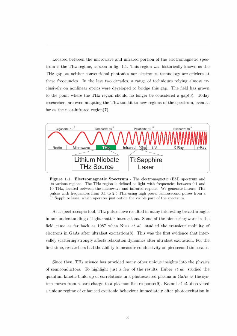
Located between the microwave and infrared portion of the electromagnetic spec-
trum is the THz regime, as seen in fig. 1.1. This region was historically known as the
THz gap, as neither conventional photonics nor electronics technology are efficient at
these freqeuncies. In the last two decades, a range of techniques relying almost ex-
clusively on nonlinear optics were developed to bridge this gap. The field has grown
to the point where the THz region should no longer be considered a gap(6). Today
researchers are even adapting the THz toolkit to new regions of the spectrum, even as
far as the near-infrared region(7).
Gigahertz: 10 Terahertz: 10 Petahertz: 10 Exahertz: 109 12 15 18
Radio Microwave Infrared UV X-Ray γ-RayTHz Vis.
Ti:SapphireLaser
Lithium NiobateTHz Source
Figure 1.1: Electromagnetic Spectrum - The electromagnetic (EM) spectrum andits various regions. The THz region is defined as light with frequencies between 0.1 and10 THz, located between the microwave and infrared regions. We generate intense THzpulses with frequencies from 0.1 to 2.5 THz using high power femtosecond pulses from aTi:Sapphire laser, which operates just outide the visible part of the spectrum.
As a spectroscopic tool, THz pulses have resulted in many interesting breakthroughs
in our understanding of light-matter interactions. Some of the pioneering work in the
field came as far back as 1987 when Nuss et al. studied the transient mobility of
electrons in GaAs after ultrafast excitation(8). This was the first evidence that inter-
valley scattering strongly affects relaxation dynamics after ultrafast excitation. For the
first time, researchers had the ability to measure conductivity on picosecond timescales.
Since then, THz science has provided many other unique insights into the physics
of semiconductors. To highlight just a few of the results, Huber et al. studied the
quantum kinetic build up of correlations in a photoexcited plasma in GaAs as the sys-
tem moves from a bare charge to a plasmon-like response(9). Kaindl et al. discovered
a unique regime of enhanced excitonic behaviour immediately after photoexcitation in
3

1. INTRODUCTION
quantum wells(10). With new sources pushing to higher frequencies multi-THz pulses,
with center frequencies of tens of THz, were shown to coherently drive carriers across
the entire brillouin zone and emit high harmonics all the way to the visible part of the
spectrum(11).
In the 0.1 to 3 THz regime, the recently developed technique of tilted-pulse-front
pumping in lithium niobate (LN) has allowed for the generation of single cycle THz
pulses capable of driving materials nonlinearly(12). The electric field measured di-
rectly in the time domain for one of these pulses is shown in fig. 1.2. A variety of new
phenomenon have been discovered, such as self-amplitude modulation by intervalley
scattering(13), coherent control of spin waves in antiferromagnetic materials(14), and
light induced interband tunneling using field-enhancing plasmonic antennae(15). The
unique nature of these sources, with huge electric fields that ramp on sub picosecond
timescales, has led to many new applications in material control(16).
In this thesis, we study how intense THz pulses from LN sources can modulate PL
in photoexcited direct-gap semiconductors (GaAs and InP). Light emission, a nanosec-
ond timescale phenomenon, is typically the last step of carrier relaxation that follows
carrier and lattice thermalization, which occurs over several picoseconds. These first
few picoseconds are an extremely complex regime, with a variety of interactions affect-
ing the dynamics. In a perfect direct gap semiconductor, almost all carriers recombine
radiatively. However, in a real semiconductor there are imperfections, such as impuri-
ties and defects, which act as channels for non-radiative recombination.
We show that an intense THz pulse affects the amount of radiative vs non-radiative
recombination, as well as the luminescence lineshape. A dynamic interplay between
photoluminescence quenching (PLQ) near the gap, and photoluminescence enhance-
ment (PLE) of hot luminescence occurs while varying the photoexcitation density.
Perhaps most interestingly, when the optical pulse preceeds, or trails the excitation
pulse by just 1 ps, no modulation of luminescence is observed. This behaviour seems to
indicate that the THz pulse modifies the initial conditions of the decay, which effects
the long term behaviour.
4

SingleCycle
PicosecondDuration
-230 kV/cm
195 kV/cm Ringing fromabsorption and
re-emission
Figure 1.2: Terahertz Pulse - The electric field, measured in the time domain atthe focus of the THz pulse. The pulse consists of a single cycle of the electromagneticfield, reaching a peak field of 230 kV/cm, while switching on and off in approximately apicosecond. The small oscillations after the peak of the THz pulse are due to absorption,and re-emission in the generation crystal, as well as water molecules in the air.
To see why, we must examine the dynamics of the first few picoseconds after exci-
tation and see how THz pulses affect this process. In the next chapter, luminescence in
semiconductors is presented in a general way in order to describe the interplay between
radiative and non-radiative decay. We then introduce the tools used to describe optical
interactions and high-field transport.
The experimental details are presented in chapter 3, including a short introduction
to the mode-locked laser, and amplifier system. The design and construction of the
intense THz pulse source is also discussed, including a guide to its alignment and oper-
ation. The methods for differential PL measurement are also presented. In particular,
5

1. INTRODUCTION
the development of a novel method for parallel detection and simultaneous background
subtraction.
Chapter 4 contains the experimental results on GaAs and InP. For GaAs, a broad
range of excitation conditions were explored and presented. Qualitatively, the data
was very similar in InP. However, several complementary studies were done in InP that
were not possible in GaAs. Chapter 5 is a discussion of the results, offering several
possible interpretations. Future experiments are proposed to elucidate the mechanism.
Chapter 6 presents our conclusions and gives perspective on the relevance of this study.
6

2
Ultrafast Excitation and
Relaxation of Semiconductors
The physics of semiconductors materials is very rich, having been studied from both
an electronics and optics perspective for decades. In order to understand intense THz
pulse interactions in photoexcited semiconductors both perspectives are required. This
is especially true in order to understand the THz pulse modulation of luminescence
where one must understand how high-field transport affects carrier distributions, and
what happens on femtosecond timescales after optical excitation that makes this regime
unique.
In general, luminescence involves the emission of light accompanying a transition
between two quantum states. The transition rate from an initial to final state, W, is
given by Fermi’s golden rule,
W =2π
~| 〈ψf |H ′ |ψi〉 |2 =
2π
~|Mif |2, (2.1)
where Mif is the matrix element of the perturbation hamiltonian, and H’, inducing the
transition. Here we have assumed all states are unique and therefore did not include
the density of final states as is typical. For the rate of spontaneous radiative decay,
luminescence, we are interested in the dipole matrix element. At any given time, the
emitted luminescence spectrum I(E) is proportional to this rate times the number of
states separated by energy E, the joint density of states g(E),
7

2. ULTRAFAST EXCITATION AND RELAXATION OFSEMICONDUCTORS
I(E) ∝ |Mif |2g(E)fi(1− ff ), (2.2)
where we have also included the probability that the initial state is occupied, fi, and
the final state is unoccupied, 1 − ff . Therefore, if we know the energy structure and
probability of occupancy f for each state, we can determine the rate and spectrum of
radiative recombination. In practice, complete knowledge of the distribution is difficult
to obtain, and photon re-absorption modifies the dynamics so that the problem is not
so simple.
Additionally, carriers can recombine non-radiatively and transfer their excess energy
to the lattice as heat. At any point in time, if there are N photoexcited carriers in the
system the recombination rate can be expressed by adding the rates of radiative, kR,
and non-radiative, kNR, recombination,
dN
dt= (kR + kNR)N. (2.3)
We have already seen how the radiative rate is a function of the distributions, energy
structure, and matrix elements. The non-radiative rate, kNR, is even more complicated,
occuring through localized centers where the precise structure is unknown. Despite
the complexity, we can write a general expression for the radiative efficiency, ηR, by
considering the fraction of carriers that recombine radiatively at time t and integrating
over the full decay,
ηR =1
N0
∫ ∞t0
N(t)
1 + kNR(t)kR(t)
dt. (2.4)
Here, we have divided by the initial carrier density, N0, for normalization. The com-
plexity of the rates is manifested in their time dependence, of which we have made no
assumptions. Using this equation, we see that there are two ways to reduce the radia-
tive efficiency: increase the non-radiative rate, kNR, or decrease the radiative rate, kR.
The converse holds for enhanced radiative efficiency.
The purpose of this chapter is to 1) introduce the basic concepts of semiconductor
physics, i.e, the electronic and vibrational structure, as well as defects or impurities,
8
2.1 Semiconductor Physics
2) Show how optically excited distributions evolve on ultrafast timescales and how this
affects the luminescence spectrum, and 3) understand how strong electric fields drive
carriers to large energies, modifying the distribution in phase space.
2.1 Semiconductor Physics
2.1.1 Crystal Lattice
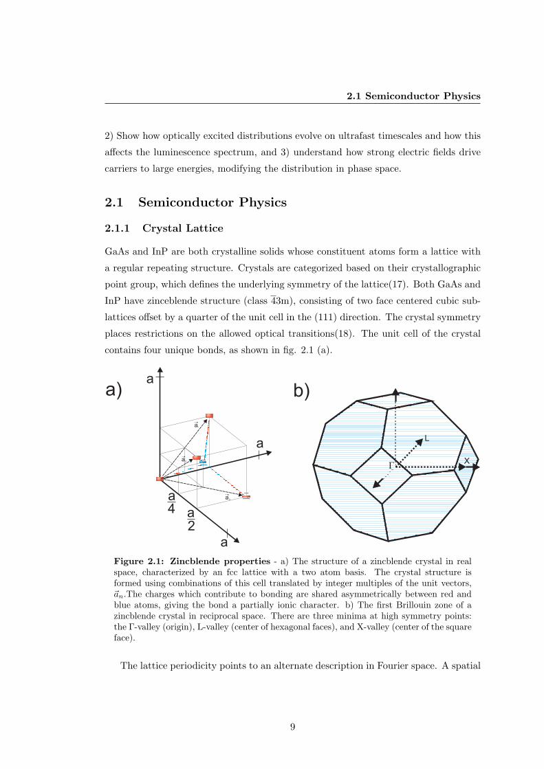
GaAs and InP are both crystalline solids whose constituent atoms form a lattice with
a regular repeating structure. Crystals are categorized based on their crystallographic
point group, which defines the underlying symmetry of the lattice(17). Both GaAs and
InP have zinceblende structure (class 43m), consisting of two face centered cubic sub-
lattices offset by a quarter of the unit cell in the (111) direction. The crystal symmetry
places restrictions on the allowed optical transitions(18). The unit cell of the crystal
contains four unique bonds, as shown in fig. 2.1 (a).
X
L
a) b)
a
a
a
2
4
a
a
a1
a2
a3
Figure 2.1: Zincblende properties - a) The structure of a zincblende crystal in realspace, characterized by an fcc lattice with a two atom basis. The crystal structure isformed using combinations of this cell translated by integer multiples of the unit vectors,~an.The charges which contribute to bonding are shared asymmetrically between red andblue atoms, giving the bond a partially ionic character. b) The first Brillouin zone of azincblende crystal in reciprocal space. There are three minima at high symmetry points:the Γ-valley (origin), L-valley (center of hexagonal faces), and X-valley (center of the squareface).
The lattice periodicity points to an alternate description in Fourier space. A spatial
9

2. ULTRAFAST EXCITATION AND RELAXATION OFSEMICONDUCTORS
Fourier transform of the lattice results in a new lattice in what is known as reciprocal
or k-space, where k is a wavevector. This space is critical to understanding optical
interactions in semiconductors, as we will show later. In k-space, a special definition
of the unit cell is chosen, called the Wigner-Seitz cell(19). It is defined, after choosing
a lattice point as the origin, as the volume closer to the origin than any other lattice
point. This cell is called the Brillouin zone, shown for a zincblende crystal in fig. 2.1
b), with the Γ, L, and X points of high symmetry labelled.
2.1.2 Electronic Structure
The energy levels resulting from level splitting when many identical atoms are brought
close together form continuous bands. In a semiconductor, all bands are either full
or empty at zero temperature. The gap between the highest valence (occupied), and
lowest conduction (empty) bands is known as the band gap. Semiconductors are essen-
tially transparent for photon energies below the gap, and opaque for photon energies
above the gap.
Many different techniques exist for calculating band structure. Tight binding or
k · p methods can give accurate band structures within several eV of the fermi level
throughout the whole Brillouin zone, with a number of adjustable parameters(20, 21).
More recently, ab-initio techniques have been developed which can calculate the full
band structure accurately with zero adjustable parameters, although they are compu-
tationally expensive(22).
While real semiconductors have many bands, for optical excitation near the bandgap
a four band model is sufficient. Here there are three valence bands, the light hole (lh),
heavy hole (hh), and split-off (SO) hole bands, and one conduction band that are im-
portant. The relevant bands are shown schematically for a direct-gap semiconductor
with zinc blende structure in fig. 2.2.
Near the band extrema, the dispersion is parabolic, and the energy as a function of
wavevector can be written as,
10

2.1 Semiconductor Physics
EEEL
X
heavy hole
light hole
split off hole
ESO
L-valley X-valley-valley
Figure 2.2: Zincblende Crystal Structure - The simplified band structure of a typicalzincblende direct-gap semiconductor, showing only the bands relevant to the current study.There are three hole bands; the light, heavy, and split off hole. In the first conduction band,there are three minima; at the Γ, L, and X points in the Brillouin zone. Here, the valleysare connected smoothly, and the structure at the extrema with negative curvature is notaccurate. There are 3 and 4 inequivalent X, and L valleys respectively, which can be seenfrom the geometry of the Brillouin zone in fig. 2.1.
E =~2k2
2m∗, (2.5)
with an effective mass m∗ determined by the curvature of the band. Non-parabolicity
can be accounted for using a wavevector dependent effective mass. The joint den-
sity of states between any two bands, g(E) in eq. 2.2, can be found in the parabolic
band approximation using the reduced mass between the two. Near the minimum, the
Γ-valley of the conduction band is essentially isotropic, while the satellite valleys (X
and L) are not. There are different longitudinal and transverse effective masses for the
X and L valleys. In the semiconductors used in this work the longitudinal mass is larger.
The valence bands are more complicated as degeneracy leads to strong interactions
between bands. The heavy and light holes are degenerate at k=0, while degeneracy
is lifted by spin-orbit coupling for the SO band. The effective masses are anisotropic,
11

2. ULTRAFAST EXCITATION AND RELAXATION OFSEMICONDUCTORS
however the 9 independent parameters (m100, m110, and m111 for each of the hh, lh,
and SO bands) can be reduced to 3 Luttinger parameters in zincblende crystals(23).
In GaAs and InP, the anisotropy is not large.
2.1.3 Phonon Dispersion
The atoms which make up the lattice are free to oscillate about their equilibrium posi-
tions. The normal modes of vibration, similar to electron energies, can be conveniently
described as a function of wavevector. With an infinite crystal, a continuous range
of energies from the zone center to the zone edge is available for each degree of free-
dom in a unit cell. For a two-atom basis, as in zincblende, this results in 6 normal
mode branches. Shown in fig. 2.3 is the normal mode dispersion along high symmetry
directions, where degeneracy reduces the number of branches to only 4.
The energy of each mode is quantized, and the quanta of crystal lattice vibration
is known as a phonon. Phonons with zero (nonzero) frequency at the zone center are
called acoustic (optical) phonons. For both acoustic and optical phonons, there are
longitudinal and transverse modes. In zincblende crystals, bonding has both covalent
and ionic character, resulting in a charge asymmetry between sublattices. This results
in a phonon with a dipole moment. The transverse optical (TO) phonon is therefore
infrared active and can interact directly with light. Longitudinal optical (LO) phonons
can interact with light indirectly by Raman (inelastic) scattering.
2.1.4 Thermal Excitations
At finite temperature, the assumption that all valence bands are full and conduction
bands empty breaks down. For systems in thermal equilibrium, the statistics governing
occupancy of excited electronic states can be described by the Fermi-Dirac distribution,
f(E) =1
e(E εF )
kbT + 1
, (2.6)
where kb is the Boltzmann constant, T is the temperature, and εF is the Fermi level, or
chemical potential. The number of electrons as a function of energy can be calculated
by multiplying this function by the energy-dependent density of states. Electrons which
12

2.1 Semiconductor Physics
L X
TA
LA
LO
TO
Figure 2.3: Zincblende Phonon Dispersion - Four non-degenerate branches ofphonons exist along high symmetry directions in the Brillouin zone, corresponding to the111 (L) and 100 (X) directions. LO (LA) refers to longitudinal optical (acoustic) phonons,and TO (TA) refers to transverse optical (acoustic) phonons. The acoustic branches havezero energy at the Γ-point, so electrons at the bottom of the band can both emit and absorbphonons. Optical phonons have non-zero energy, such that there is a threshold electronenergy for emission.
occupy states in the conduction band leave behind a net positive charge in the valence
band. This can be conveniently described as a hole, a particle which behaves like a
positively charged electron.
In non-equilibrium situations, when no coherence exists in the system, the dis-
tributions of electrons and holes can be calculated using the eq. 2.6 with separate
Fermi levels for electrons and holes that depend on the level of excitation. When these
quasi-Fermi levels are in the conduction (valence) band for electrons (holes), there is
a population inversion, and stimulated emission of radiation can lead to optical gain.
For a given carrier density in the valence or conduction band, NC,V , the quasi-Fermi
level can be calculated by inverting the equation,
13

2. ULTRAFAST EXCITATION AND RELAXATION OFSEMICONDUCTORS
NC,V =
∫ ±∞EC,V
gC,V (E)f(E)dE, (2.7)
where f(E) is given by eq. 2.6, EC,V is the energy of the bottom/top of of the conduc-
tion/valence band, and gC,E(E) is the density density of states in the conduction or
valence band. This is essentially a statement of particle conservation.
The statistics of phonon excitations behave differently than electrons, as they are
bosons rather than fermions. Here, the Bose-Einstein distribution deterimines the
occupancy of each mode,
f(E) =1
eEkbT − 1
. (2.8)
This differs from eq. 2.6 by the sign in the denominator, as well as the lack of a chemical
potential. This reflects the fact that phonon number is not conserved and a phonon
can be added with no cost of energy analogous to the statistics of photons. However,
some work suggests that in non-equilibrium situations, photons can have a non-zero
chemical potential, and it is possible that the same principle holds for phonons(24).
In our experiments, equilibrium occupancy of optical modes is relatively low, as the
optical phonon energy is comparable to kbT at room temperature. However, large non-
equilibrium populations, or hot phonons, can be excited during electron relaxation.
Using Raman scattering, where the relative heights of the absorption and emission
peaks give an indication of occupancy, effective temperatures over 1000 K have been
reported for optical phonons near the zone center(25).
2.1.5 Localized States
The electron and phonon dispersions discussed so far have been for semiconductors with
a perfect lattice that is infinite in extent. In real semiconductors, impurites, interstitial
atoms, vacancies, and bulk and surface defects all have electronic and vibronic states.
If the density is low enough that no aggregates form, these imperfections result in local-
ized electronic and vibrational modes. Here, a k-space description does not necessarily
14

2.2 Dynamics
apply in the same way, as a localized state does not share the same infinite periodicity
as the lattice.
The nature of the electronic states of bulk imperfections is quite variable. In many
cases, they can be thought of analogously to molecules or atoms embedded in the lattice
with discrete vibrational and electronic levels. When these levels are close to the band
edges they are considered traps, and they act as scattering centers for conduction band
electrons. When they are near the middle of the gap they are called deep levels where
non-radiative recombination can occur.
A configurational coordinate diagram is often used to describe these centers. The
configurational coordinate diagram is analogous to reaction coordinates from chemistry,
where many degrees of freedom are simplified to one abstract coordinate(26). A simple
example of one of these diagrams is shown in fig. 2.4. There is an excited and ground
electronic state, each with multiple vibrational levels. When the system can transition
directly from the excited to ground state without a change of energy, or reaction coor-
dinate, a non-radiative transition can occur.
After transitioning to the ground electronic state, the system can vibrationally re-
lax by sequential emission of phonons to the surrounding lattice. In this diagram it
is apparent that this transition can occur when the system is vibrationally excited,
so that higher temperatures result in faster non-radiative rates. The relaxation rate
of these types of centers is governed by Shockley-Reed-Hall recombination(27). This
type of recombination is dominant in indirect-gap semiconductors such as silicon or ger-
manium, where the carrier lifetime is on the order of microseconds at room temperature.
2.2 Dynamics
In our experiments, we are interested in using the tools developed so far to under-
stand dynamical processes, such as transport and photoexcitation. In most cases, a
semiclassical treatment where the Boltzmann transport equation,
∂tf + v(k) · ∇rf +Fext
~· ∇kf = (∂tf)scat, (2.9)
15

2. ULTRAFAST EXCITATION AND RELAXATION OFSEMICONDUCTORS
Configuration Coordinate
En
erg
y
Qg0 Qe0
IntersectingCurves
Figure 2.4: Configurational Coordinates - Energy levels of a non-radiative center, asa function of configuration coordinate Q. For the example of an impurity atom, Q wouldbe the average distance of neighboring atoms. The dotted green (red) lines indicate thevibrational levels of the electronic ground (excited) states. In the vibrationally and elec-tronically excited state, the system can transition directly to a highly vibrationally excitedground electronic ground state where the curves intersect (indicated on the diagram). Se-quential release of phonons to the crystal lattice completes the process of non-radiativerecombination.
16

2.2 Dynamics
is used to understand how the distribution, f(r,k), of particles evolves in phase space
as a function of time(28). Here, the terms on the left hand side describe the behaviour
of a distribution of free particles with velocity v(k) in an external field, Fext. The
scattering term, on the right hand side, arises from processes which interupt the free
particle motion. Rather than deal with calculating the effect of each individual phonon
or impurity, for example, they are instead treated statistically. Scattering events re-
distribute electrons among the states at a rate which can be determined from Fermi’s
golden rule. In this case the matrix element depends on the nature of the scattering
mechanism.
In ultrafast experiments, we generate a new distribution within a narrow range of
energies. We are then interested in how it evolves as a function of time thermalizing
with itself and with the lattice before relaxing back to an unexcited state. In high-field
transport, we study how carriers are redistributed within the excited state due to an
external field. Here, we will outline some general features of the evolution of a distri-
bution in such experiments.
2.2.1 Absorption of Light
The dipole matrix element is used to determine the rate of absorption, similarily to the
rate of emission, and is typically a constant value near the band edge. The absorption
coefficient scales proportionally to the joint density of states,
α ∝ µ3/2√Eγ − Eg, (2.10)
where µ is the reduced effective mass of the conduction and valence bands, and Eγ is
the photon energy. The absorption coefficient is zero for photon energies smaller than
the gap, and for larger energies increases proportionally to the square root of the excess
energy, Eγ − Eg. The effective masses in GaAs and InP are similar, and for the same
excitation fluence and center frequency the absorption coefficient in InP is higher than
that of GaAs as the bandgap of InP is smaller than GaAs.
17

2. ULTRAFAST EXCITATION AND RELAXATION OFSEMICONDUCTORS
Here we have assumed linear absorption. Following this assumption, we can make
an estimate of the carrier density. The intensity of light, or number of photons, decays
exponentially as a function of depth in a material. To simplify the calculation, we
assume uniform carrier density in a cylinder of radius r (the excitation spot radius),
and height δ = α−1. For an incident pulse with energy W and center frequency f the
carrier density is,
ρ =N
V=W
hf
T(1− e−1
)πr2δ
, (2.11)
where T is the transmission coefficient, 1-e−1 is the fraction of carriers absorbed in
within penetration depth, and, h is the usual Plancks constant. In terms of eq. 2.9,
optical excitation can be thought of as injecting carriers with well-defined energy and
position. The distribution of injected carriers, before scattering, is similar to a set of
gaussian functions with one for each valence band from which carriers can be excited.
This calculation assumes linear absorption, which breaks down on short timescales
and high excitation densities. Spectral hole burning decreases the absorption co-
effiecient in the case where the excited state occupancy fills more rapidly than it is
depleted by scattering processes(29). At extremely high densities, all of the excited
states become occupied, and the absorption edge moves to higher energies, analogous
to the Burstein-Moss shift where there is a blueshift of the absorption edge due to
doping(30). At the excitation densities used in this study, nonlinear absorption is
likely to occur. As a result, trends in data will be discussed in terms of pump power,
only providing an estimate of carrier density.
2.2.2 Coulomb Scattering
For carrier-carrier scattering, the perturbation hamiltonian is the couloumb interaction
between charged particles. The scattering rate is strongly density dependent, with time
constants ranging from tens of picoseconds to tens of femtoseconds for carrier densi-
ties of 1015 and 1018 respectively cm−3. Electron-electron, electron-hole, and hole-hole
scattering all occur at slightly different rates, proceeding most rapidly for particles with
18

2.2 Dynamics
similar effective masses.
In our experiments with high excitation density, carrier-carrier scattering efficiently
thermalizes electrons and holes on timescales shorter than the duration of the excitation
pulse. The electron and hole distributions can be described by eq. 2.6 almost instanta-
neously. As a result, the PL spectrum contains no remnant structure of the excitation
pulse. This is not the case for low excitation density and low temperature(31).
Coulomb scattering is an elastic process, and the carrier system does not dissipate
energy in this phase of relaxation. As the timescale for carrier scattering is much more
rapid than phonon scattering, a hot electron distribution with effective an temperature
much higher than ambient is formed.
In one sense, carrier-carrier scattering does not play an important role during trans-
port. It can be ignored in the simulation of equilibrium transport using the Boltzmann
equation. However, in another sense, the collective response of electrons, a plasmon,
governs the AC conductivity. For a free electron gas the dielectric constant is given by,
εr(ω) = 1−(Ne2
ε0m∗
)1
ω2 + iω/τ, (2.12)
where, εr is the relative dielectric constant, e is the elementary charge, ε0 is the per-
mittivity of free space, ω is the frequency of the electric field, and τ is the scattering
rate(32). The quantity in brackets is the square of the plasma frequency, ωp,
ωp =
(Ne2
ε0m∗
)1/2
, (2.13)
The Coulomb interaction between electrons and holes is also responsible for the
formation of bound states (excitons) with energy in the forbidden gap(33). Generally,
the contribution of excitons to optical properties can be neglected when the binding
energy is much lower than the ambient temperature. This is the case in our experi-
ments. However, Kaindl et al. have observed strongly enhanced excitonic behaviour
in quantum wells, even with ambient temperature several times that of the binding
energy(10).
19

2. ULTRAFAST EXCITATION AND RELAXATION OFSEMICONDUCTORS
2.2.3 Carrier-Phonon Scattering
Electrons can also scatter off of lattice vibrations, where the perturbation hamiltonian
can take several forms. The local variation in lattice constant of longitudinal oscilla-
tions results in a change in bandgap. This is known as deformation potential scattering,
and the resulting matrix element is independent of wavevector. In zincblende semicon-
ductors, the dipole moment of the phonon results in polar optical electron-phonon
coupling, governed by a Frolich Hamiltonian(34). Here the coupling strength near k=0
is strong, but drops off as the inverse square of the wavevector.
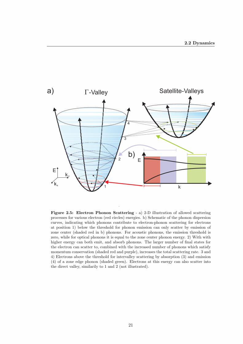
While electrons can absorb a phonon anywhere in the lattice, there is a threshold
for phonon emission given by the zone center phonon energy. The zone center acoustic
phonon energy is zero, so that acoustic phonon emission is always possible. Conduc-
tion band electrons at the bottom of the Γ-valley can only scatter off of low wavevector
phonons.
As the energy increases, larger wavevector transfer is possible, and there is a higher
density of final states. The result is an increasing scattering rate with carrier energy.
Carriers within one LO phonon energy of the X or L minima can undergo intervalley
scattering, which occurs via deformation potential interaction with zone edge phonons.
These principles are summarized in fig. 2.5.
After ultrafast excitation, electron-phonon coupling is responsible for bringing the
lattice and carrier system to thermal equilibrium over several picoseconds. The scatter-
ing rate for acoustic and optical phonons are similar(35), however the cooling process is
dominated by optical phonons, as more energy is exchanged with each scattering event.
At high excitation densities, the cooling process can be slowed due to the presence of
hot phonons, as the statistical weight of phonon absorption is increased relative to that
of emission(36).
Intervalley scattering (3 and 4 in fig. 2.5) is also important in both optical excita-
tion and high-field transport. If photoexcited electrons are injected with high enough
energy to undergo intervalley scattering, the majority of carriers will first scatter to
20
2.2 Dynamics
E
kx
k y
Satellite-Valleys-Valleya)
b)E
k1
2
3
4
Figure 2.5: Electron Phonon Scattering - a) 2-D illustration of allowed scatteringprocesses for various electron (red circles) energies. b) Schematic of the phonon dispersioncurves, indicating which phonons contribute to electron-phonon scattering for electronsat position 1) below the threshold for phonon emission can only scatter by emission ofzone center (shaded red in b) phonons. For acoustic phonons, the emission threshold iszero, while for optical phonons it is equal to the zone center phonon energy. 2) With withhigher energy can both emit, and absorb phonons. The larger number of final states forthe electron can scatter to, combined with the increased number of phonons which satisfymomentum conservation (shaded red and purple), increases the total scattering rate. 3 and4) Electrons above the threshold for intervalley scattering by absorption (3) and emission(4) of a zone edge phonon (shaded green). Electrons at this energy can also scatter intothe direct valley, similarily to 1 and 2 (not illustrated).
21

2. ULTRAFAST EXCITATION AND RELAXATION OFSEMICONDUCTORS
satellite valleys before relaxing to the bottom of the Γ-valley. This leads to a slow PL
rise time and broadened spectrum, as the Γ-valley density is low and carrier tempera-
ture high while electrons scatter back from satellite valleys.
For high field transport in polar semiconductors, the drift velocity first overshoots
the equilibrium value before the majority of carriers scatter to satellite valleys, where
the effective mass is higher. The figure of merit for determining the fields required for
velocity overshoot is the Gunn field, which is on the order of 10 kV/cm(37). The peak
THz fields in free space used in this work are on the order of 200 kV/cm, which is much
higher than the Gunn field. However, the transmitted field could be smaller than this,
and the Gunn field could be relevant.
Intense THz fields drive intervalley scattering on sub-cycle timescales, modulating
the optical conductivity by increasing the effective mass and scattering rate in eq. 2.12.
This leads to self amplitude modulation and rectification of the incident pulse(13). This
rectification leads to a spatial separation of the electron and hole distributions.
2.2.4 Surface Effects
A high density of localized states exists at surfaces or interfaces. At room temperature
in equilibrium, electrons and holes diffuse towards the surface. As the effective mass of
electrons is lower than holes, more electrons end up trapped in the surface, resulting in
a built-in voltage and band bending. On excitation, a transient current surge occurs,
spatially separating electrons and holes.
Additionally, both electrons and holes diffuse into the substrate, because of the
gradient density. Electrons diffuse more rapidly into the substrate than holes, due to
mass asymmetry, which is another source of transient current normal to the surface.
This process, known as the photodember effect, results in spatial separation of elec-
trons and holes(38). These current surges can be studied by collecting the emitted THz
radiation(39).
22

2.3 Summary
After any transient dynamics have died down, there is a net drift of electrons into
the substrate, once again due to the charge gradient, as well as towards the surface.
With an untreated surface with high surface state density, drift towards the surface
is limited by the drift velocity. This diffusion is associated with recombination as all
carriers which reach the surface recombine non-radiatively. It is parameterized by the
surface recombination velocity(40).
2.3 Summary
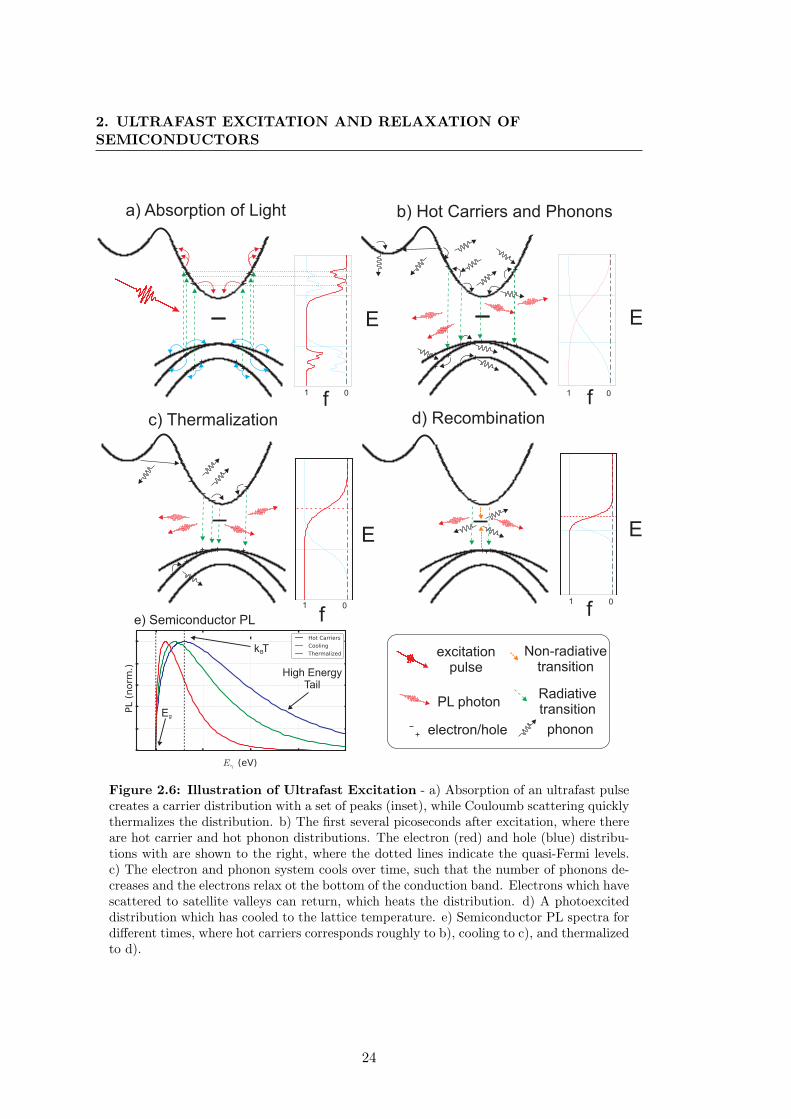
We will conclude with a brief summary of ultrafast excitation, shown in fig. 2.6. When
an ultrafast pulse is incident on a semiconductor, a distribution of carriers with a narrow
range of energies is generated, however, in our experiments Couloumb scattering ther-
malizes the distribution on timescales compared to the excitation pulse. For excitation
near the gap, only a small number of carriers scatter to the satellite valleys, as in 2.6 a).
Over the next several picoseconds, there are both hot electron and hot phonon dis-
tributions as in 2.6 b). In this situation, carriers are more likely to absorb phonons
than in equilibrium situations, and the cooling is slowed. PL in this regime is has a
very broad spectrum which is considered hot luminescence. While the hot phonons are
decaying, the electrons are also relaxing down to the bottom of the band. Any carriers
scattered to the satellite valleys act as a resevoir of hot carriers as indicated by the
carrier returning to the direct valley in 2.6 c). This Keeps the distribution hotter simi-
larily to the hot-phonon effect. When excited in the presence of the intense THz pulse
electric field many more carriers will scatter to the satellite valleys. As well as acting
as a hot-carrier resevoir, this will slow the rise time of the luminescence by reducing
the density in the Γ-valley.
After the carrier and phonon systems have thermalized, the remaining excited car-
riers must still recombine. In this regime, the full-width half-max (FWHM) of the
luminescence spectrum is approximately kBT . In this final stage we have also included
a channel for non-radiative recombination. In principle it should be included in all
figures as it is a probablistic process. Generally the timescales are much longer than
23
2. ULTRAFAST EXCITATION AND RELAXATION OFSEMICONDUCTORS
a) Absorption of Light b) Hot Carriers and Phonons
c) Thermalization d) Recombination
e) Semiconductor PL
Eg
k TB
High EnergyTail
excitationpulse
PL photon
electron/hole phonon
Non-radiativetransition
Radiativetransition
f
E
f
E
f
E
f
E
01 01
01 01
Figure 2.6: Illustration of Ultrafast Excitation - a) Absorption of an ultrafast pulsecreates a carrier distribution with a set of peaks (inset), while Couloumb scattering quicklythermalizes the distribution. b) The first several picoseconds after excitation, where thereare hot carrier and hot phonon distributions. The electron (red) and hole (blue) distribu-tions with are shown to the right, where the dotted lines indicate the quasi-Fermi levels.c) The electron and phonon system cools over time, such that the number of phonons de-creases and the electrons relax ot the bottom of the conduction band. Electrons which havescattered to satellite valleys can return, which heats the distribution. d) A photoexciteddistribution which has cooled to the lattice temperature. e) Semiconductor PL spectra fordifferent times, where hot carriers corresponds roughly to b), cooling to c), and thermalizedto d).
24
2.3 Summary
the other listed processes so that this channel of recombination was only included in
the final diagram.
The PL spectrum from each of these regimes is shown in fig. 2.6 e), it was cal-
culated using eqs. 2.1 and 2.5. The broadest spectrum is associated with the earliest
timescales, and the narrow with the longest. The lineshape is asymmetric, reflecting
the nature of the density of states which increases with energy. Real semiconductor
luminescence does not precisely follow this curve and there are always photons emitted
with sub-band-gap energy.
Some studies associate the sub-gap luminescence emission from band tail states,
e.g., the Urbach tail(41). By assuming a functional form for the tail states and con-
voluting these with the regular semiconductor states it is possible to fit the full PL
spectrum(42). Alternatively, the mid-gap PL can be treated as a many-body effect,
where optical emission occurs with the simultaneous emission of a plasmon broadening
the emission linewidth(43). Interpreting both the emission as either broadened transi-
tions or from mid-gap states reproduces experimental data well.
25
3
Experimental Details
In the previous chapter, we introduced the physics of semiconductors, and talked about
ultrafast excitation and high-field transport. The tools we use to probe these ma-
terials are amplified femtosecond pulses from a Ti:Sapphire laser system (Coherent
Micra/Legend) and intense THz pulses generated in LN by tilted-pulse-front optical
rectification (OR). The laser amplifier operates at 1 kHz and outputs 3.5 mJ, 800 nm,
pulses with 50 fs duration. The THz source is homebuilt, and characterized using a
combination of wavefrom, pulse energy, and spot profiling, using EO sampling, a py-
roelectric detector, and thermal imager respectively. Typical pulse energies of 2.0 µJ ,
and e−2 spot diameters of 1.8 mm result in peak electric fields of up to 230 kV/cm as
measured by EO sampling.
The THz pulse is collected and focused onto GaAs or InP wafers using off-axis
parabolic mirrors. The wafers are simultaneously photoexcited collinearly using near
infrared (NIR) pulses split off from the same Ti:Sapphire amplifier. PL is collected non-
collinearly and focused into an optical fiber, then measured using either 1) a photodiode
to study integrated change, or 2) a monochromator and CCD (charge-coupled device)
array for parallel detection or a slit and avalanche photodiode (APD) for single channel
detection of the differential spectrum. Fig. 3.1 is a schematic of the experimental setup.
In the following sections, each component will be described in more detail.
26

Electro-optic Sampling
ModelockedLaser
IntenseTHz Source
PulseCompressor
Auto-correlator
Quad Detectors
SemiconductorSample
PulseCompressor
PulseStretcher
RegenerativeAmplifier
Beamsplitter
Polarizer
/2-Plate
CoarseDelay Stage
FineDelay Stage
PL Detection
80 MHz Ti:Sapph
1 kHz Amplifier
Luminescence
THz Pulse
AlignmentMirrors
Figure 3.1: Schematic of Experiment Setup - A Ti:Sapphire laser oscillator (CoherentMicra) seeds a 1 kHz regenerative amplifier (Coherent Legend). The output of the amplifieris split into several beams used for THz generation by optical rectification of tilted pulsefronts in lithium niobate, photoexcitation of luminescent semicondutors, and electro-opticalsampling. The components are roughly color coded as Coherent Inc. products (pink), THzsource components (purple), THz modulation of PL (blue), and alignment tools (orange).
27

3. EXPERIMENTAL DETAILS
3.1 Laser System
3.1.1 Oscillator
The laser oscillator (Coherent Micra) is a mode-locked, 80 MHz repetition rate Ti:Sapphire
lasers pumped by the second harmonic of a continuous wave (CW) Nd:YVO4 diode
pumped laser (Coherent Verdi V5), which outputs 5 W at 532 nm. It is passively
mode-locked, based on the principle of kerr-lensing, where the self focusing of an in-
tense pulse leads to better overlap with the pump in the gain medium. The cavity
therefore favors mode-locked vs. CW operation(44). A pulse compressor consisting of
a prism pair is inserted into the cavity, as seen in fig. 3.2 a). Once mode-locked, pulse
propagation in the cavity behaves as a soliton resulting in a stable regime where the
positive group velocity dispersion (GVD) of the Ti:Sapphire crystal is balanced by the
negative GVD of the prism compressor(45).
The pulse characteristics can be tuned by translating the prisms in and out of the
beam to adjust the group delay. An adjustable slit can also be used to physically block
portions of the spectrum. In fig. 3.2 b)-d), the laser spectrum is shown tuned to 40 nm,
50 nm, and 80 nm bandwidth respectively. More insertion results in more bandwidth,
however with too much negative GVD the soliton mode-locking regime is lost, and other
mode-locking mechanism can dominate(46, 47). Another common problem is shown in
3.2 d), the sharp peak in the spectrum is due to CW breakthrough. It is important
to avoid this when tuning. We typically operate the laser in the 40 nm bandwidth
condition for 2 reasons: 1) as bandwidth increases, the secondary peak (seen at 750 nm
in fig. 3.2 c ) increases in amplitude, and 2) it results in more stable long term operation.
3.1.2 Amplifier
The pulse train of the oscillator is routed to a stretcher, and used to seed a chirped
pulse regenerative amplifier (Coherent Legend). The pulse is first stretched to sev-
eral hundred picoseconds, to prevent damage of the crystal during amplification(48).
Pulses are injected into a secondary laser cavity at 1 kHz repetition rate using a pock-
els cell, where they make approximately 15-18 round trips before being ejected by a
second pockels cell in combination with a brewster window. The crystal in this cavity
28

3.1 Laser System
Verdi
Ti:Sapph crystal
prism
beam dump532 nm pump
end mirrors800 nm pulse
a)
d)c)
b)
slit
Figure 3.2: Laser Oscillator - a) Schematic layout of the mode-locked laser system. b)-d) Laser spectrum tuned for various conditions. A combination of translations from bothprisms was used to obtain these spectra. Inserting more of the prism into the beam typicallyresults in more bandwidth, however too much makes the laser makes the system unstable.The spectrum is adjusted by translating the prisms in the cavity, which compensate fordispersion in the Ti:Sapphire crystal. In c), a small peak in the spectrum can be seen at750 nm. The origin of this behaviour is not known, and great care must be taken duringalignment to minimize this peak and obtain a Gaussian spectrum. In d), the peak in thespectrum is due to CW breakthrough. The amplifier should not be run with this featurepresent in the spectrum.
29

3. EXPERIMENTAL DETAILS
is pumped by a 30 W Q-Switched 532 nm laser (Coherent Evolution). The 800 nm
pulses are recompressed after ejection from the regenerative amplifier.
The bandwidth of the output of the amplifier is in general less than that of the
oscillator, with a nearly Gaussian profile centered near 800 nm, with a FWHM of 26
nm. Although the exact pulse characteristics change with alignment, an example of the
spectrum is shown in fig. 3.3 a). Fig. 3.3 b) shows the effects of the high power beam
propagating through a glan-laser polarizer (Thorlabs) without attenuation but with a
modified spectrum. If the laser power is attenuated before the polarizer, the spectrum
remains unmodified. This nonlinear behaviour is characteristic of SPM (self-phase
modulation), and should be avoided as it introduces undesireable pulse qualities.
a) b)
Figure 3.3: Amplifier Spectrum - a) Laser spectrum after amplification, showing anearly Gaussian profile with bandwidth of 26 nm, lower than that of the oscillator. b)Laser spectrum after a glan laser polarizer without attenuation, displaying a modifiedspectrum. For the results presented in this thesis, a neutral density filter is used beforethe polarizer to prevent this effect.
The temporal behaviour of the pulse is measured using an autocorrelator, as shown
in fig. 3.4 a). Here, the laser pulse is passed through a beamsplitter, and the pulses are
mixed in a beta barium borate (BBO) crystal crossing at a small angle. The intensity
of the second harmonic, ISHG, is measured as a function of delay, τ ,.
ISHG(τ) =
∫ ∞−∞
IFF (t)IFF (t− τ)dt, (3.1)
30
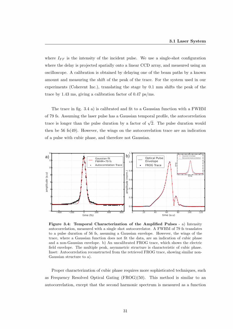
3.1 Laser System
where IFF is the intensity of the incident pulse. We use a single-shot configuration
where the delay is projected spatially onto a linear CCD array, and measured using an
oscilloscope. A calibration is obtained by delaying one of the beam paths by a known
amount and measuring the shift of the peak of the trace. For the system used in our
experiments (Coherent Inc.), translating the stage by 0.1 mm shifts the peak of the
trace by 1.43 ms, giving a calibration factor of 0.47 ps/ms.
The trace in fig. 3.4 a) is calibrated and fit to a Gaussian function with a FWHM
of 79 fs. Assuming the laser pulse has a Gaussian temporal profile, the autocorrelation
trace is longer than the pulse duration by a factor of√
2. The pulse duration would
then be 56 fs(49). However, the wings on the autocorrelation trace are an indication
of a pulse with cubic phase, and therefore not Gaussian.
a) b)
Figure 3.4: Temporal Characterization of the Amplified Pulses - a) Intensityautocorrelation, measured with a single shot autocorrelator. A FWHM of 79 fs translatesto a pulse duration of 56 fs, assuming a Gaussian envelope. However, the wings of thetrace, where a Gaussian function does not fit the data, are an indication of cubic phaseand a non-Gaussian envelope. b) An uncalibrated FROG trace, which shows the electricfield envelope. The multiple peak, asymmetric structure is characteristic of cubic phase.Inset: Autocorrelation reconstructed from the retrieved FROG trace, showing similar non-Gaussian structure to a).
Proper characterization of cubic phase requires more sophisticated techniques, such
as Frequency Resolved Optical Gating (FROG)(50). This method is similar to an
autocorrelation, except that the second harmonic spectrum is measured as a function
31

3. EXPERIMENTAL DETAILS
of time delay, and the signal is given by,
IFROG(ω, τ) =
∣∣∣∣∫ ∞−∞
E(t)E(t− τ)eiωtdt
∣∣∣∣2 (3.2)
Using a phase retrieval algorithm, the electric field envelope can be recovered from
the FROG trace(51). In chapter 4, results will be presented where the THz modulation
of PL is strongly affected by the compressor setting. Some indications have shown
asymmetry with respect to chirp direction. In order to understand the origin of these
effects, we are currently developing an implementation of frequency-resolved optical
gating(52). A recovered trace is shown in fig. 3.4 b).
These results are prelimanary and the time axis is uncalibrated, however, this figure
is included to give a possible interpretation of the asymmetry in some of our results.
The multi peak structure of the envelope is a characteristic of cubic dispersion which is
a common feature of amplified pulses. The inset shows the solution to eq. 3.1 with the
reconstructed FROG trace as the input, i.e, the autocorrelation of the FROG trace.
The wings on the trace are qualitatively similar to the experimentally acquired auto-
correlation in 3.4 a).
3.1.3 Beam Routing
After ejection from the cavity, the pulse is immediately passed through an 80-20 beam
splitter. Separate compressors are used for each beam, with the 80% going to a home
built grating compressor, and the 20% beam going to the Legend amplifier internal
compressor. In this way, the pulse duration for the THz generation beam can be con-
trolled separately from the other beams. The 20% power beam is further split into
high, medium, and low power beams used for photoexcitation, electro-optic sampling,
and diagnostics respectively.
The high and medium power beams pass through both rough (92 cm travel) and
fine (15 cm travel) computer-controlled delay stages. This results in a full scan window
of 107 cm, or 7.1 ns. For a given experiment, the rough stage is typically fixed in a
convenient location which puts t0, the point where any two beams arrive at the same
32

3.2 Intense THz Source
time, near the middle of the fine delay stage.
a) b)
Figure 3.5: Effect of clipping - Image of the laser spot on a white screen taken witha phone camera. In a) the laser propagates through a wide open aperture. Careful ex-amination reveals a very dim strip above the main spot of the laser. This feature is moreeasily visible to the naked eye, and is present after amplification. In b), the aperture ispartially closed, and the screen is placed approximately 50 cm away, showing interferencefringes. The fringes, and other features, generally become more prominent, and otherfeatures develop with increasing propagation distance.
Care must be taken to preserve laser pulse quality during propagation along the
bench. Clipping results in interference fringes in the mode of the laser, as seen in fig.
3.5. The beam size at the delay stages is almost as large as the apertures, and proper
beam pointing at these points is critical. To facilitate this alignment, a small amount
of the low power (diagnostics) beam is split off and sent to a quad detector in two
locations. The first two mirrors after the compressor are used to balance the quads on
a daily basis.
3.2 Intense THz Source
The 80% beam from the amplifier is used for intense THz generation using tilted pulse
front pumping (TPFP) OR in LN(12). Here we will not present an in depth theoretical
description of THz generation by OR, which can be found in many papers, for example
refs.(53, 54, 55, 56). Instead, we simply give the reader a short, intuitive description
33

3. EXPERIMENTAL DETAILS
of the technique. In OR, an ultrafast pulse propagating in an EO crystal produces
a transient polarization at THz frequencies by beating between the various frequency
components (difference frequency generation in the Fourier domain).
In index-matched crystals, the polarization radiates a field and the amplitude grows
linearly with propagation distance. Here, constructive interference during propagation
occurs across the full pulse front, and a spatially-extended high power pulse can be
used, as seen in fig. 3.6 a). In index mismatched crystals, a point optical source
can be used and constructive interference results in a Cherenkov cone of radiation. A
spatially-extended pulse cannot be used in the same way due to the lack of construc-
tive interference along the pulse front(57). Instead, an extended source can be used by
tilting the intensity front along the Cherenkov cone angle θ, as seen in fig. 3.6 b).
a) b)cnopt
cnTHz
Figure 3.6: Optical Rectification - In THz generation, the emitted radiation is de-pendent on phase matching. a) Dipole radiation generated at different times (signifiedby the increasing size of the black circles) in a phase matched crystal propagates at thesame velocity as the generation pulse and constructive interference occurs collinearly. Thesource can be extended spatially and constructive interference still occurs (signified by theblue and green dotted curves). b) Dipole radiation in a phase mismatched crystal such asLN creates a Cherenkov cone. THz generated from a spatially extended source interferesconstructively if the intensity front of the pump pulse is tilted along the angle θ (top right).
After the generation crystal, THz pulses are collected and focused with off-axis
parabolic mirrors. Pulse characterization is done using a combination of a pyroelec-
tric detector for pulse energy (Spectrum Detector), a thermal imager consisting of an
array of pyroelectric elements (Electrophysics), or electro-optic sampling in a gallium
34

3.2 Intense THz Source
phosphide (GaP) crystal. The arrangement is shown in fig. 3.7.
3.2.1 Pulse Front Tilting Optics
The beam is first reduced by a factor of 2 using a Keplerian telescope arrangement
with 200 and -100 mm focal length lenses. Several demagnification factors were tested,
and this lens combination was chosen as it resulted in the highest conversion efficiency
based on energy measured by a pyroelectric detector. A diffraction grating with groove
density N=1800 ln mm−1 angularly disperses the beam to induce pulse front tilt, and
a 4f plano-convex sperical lens system images the pulse into the crystal.
The 4f imaging configuration was chosen to reduce spatio-temporal distortion, where
the imaging of an angularly dispersing pulse introduces temporal spreading proportional
to the distance from the axis of the lenses(58). It should be noted that some groups
use cylindrical (59) instead of spherical lenses to remove temporal aberrations in the
vertical dimension. As the pulse is not angularly dispersing in the vertical dimension,
the temporal smearing should be small(60). A direct comparison between cylindrical
and spherical lenses has not yet been published.
The focal lengths of the lenses are 125 mm and 75 mm, resulting in a demagnifica-
tion factor D=1.67. This demagnification-grating combination satisfies the conditions
specified in ref. (55). The design criteria is meant to minimize the pump pulse duration
along the intensity front, avoiding imaging distortion. Finally, based on the demagnifi-
cation, D, and groove density per unit length, N, we can calculate the diffraction angle
β which results in required pulse front tilt (γ = 63),
tan(γ) = − NλopD
nLN cos(β), (3.3)
where, nLN is the index of LN at the pump wavelength, λop=800 nm, and β is the
diffraction angle given by,
Nλop = sin(α) + sin(β) (3.4)
where α is the angle of incidence. The required angle of incidence is therefore 36.8,
resulting in a diffraction angle of 57.2. These parameters are summarized in fig. 3.7. A
35
3. EXPERIMENTAL DETAILS
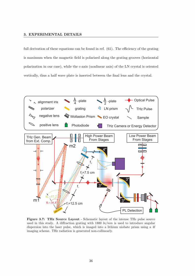
full derivation of these equations can be found in ref. (61). The efficiency of the grating
is maximum when the magnetic field is polarized along the grating grooves (horizontal
polarization in our case), while the c-axis (nonlinear axis) of the LN crystal is oriented
vertically, thus a half wave plate is inserted between the final lens and the crystal.
f =12.5 cm
f
f
f =7.5 cm
PL Detection
THz Camera or Energy Detector
grating
EO crystal
polarizer
-plate
positive lens Photodiode
Optical Pulse
THz Pulse
Wollaston Prism
Low Power BeamFrom Stages
THz Gen. Beamfrom Ext. Comp.
LN prism
q =57.2D
q =36.8I
1800 ln/mm
4"
3"
3"
3"1
2
2
1
High Power BeamFrom Stages
4
negative lens
alignment iris -plate2
Sample
m1
m2
Figure 3.7: THz Source Layout - Schematic layout of the intense THz pulse sourceused in this study. A diffraction grating with 1800 ln/mm is used to introduce angulardispersion into the laser pulse, which is imaged into a lithium niobate prism using a 4fimaging scheme. THz radiation is generated non-collinearly.
36

3.2 Intense THz Source
3.2.2 THz Routing Optics
Gold coated, 90 off-axis parabolic mirrors are used to collect and focus the emitted
THz radiation, as shown in fig. 3.7. The mirror arrangement was modelled after that
of ref. (62) where 4” and 3” focal length mirrors collect and focus the THz radiation
respectively. The 4” parabolic was chosen such that diffraction of a Gaussian pulse
with a beam waist of w0 = 1 mm at the source, and 0.5 THz center frequency (λ = 0.3
mm) would have a beam waist, w, large enough to fill the 2” aperture of the mirror at
distance x=4” from the focus, calculated using,
w2(x) = w20
[1 +
(λx
πw20
)]. (3.5)
The 3” focal length of the focusing mirror is chosen to achieve a smaller beam waist at
sample position. Additionally in our set up, a mirror can be inserted in the collimated
section before the focus optic in order to measure the energy or profile of the THz pulse.
Two 3” focal length mirrors are placed after the sample position to route the beam to a
secondary focus for EO sampling. Many groups use an alternative arrangement where
a beam expanding mirror placed immediately after the source crystal to achieve spot
sizes approaching the diffraction limit, as in ref. (59).
3.2.3 Electro-Optic Sampling Setup
In this study a 200 µm thick [110] GaP active layer, optically bonded to a 2 mm thick
[100] GaP wafer, was used for EO sampling. The active layer of the EO crystal is
placed at the focus of the final parabolic mirror with the field oriented in the [110]
direction. The pockel’s effect from the THz electric field induces a birefringence in
the crystal at optical frequencies that is sampled by an initially linearly polarized co-
propagating probe pulse. In velocity matched crystals, over distances less than the
walk off length, the differential phase retardation ∆φ is linearly proportional to the
instantaneous electric field of the THz pulses according to,
∆φ =ωL
cn3
0r41ETHz, (3.6)
enabling measurement of both the amplitude and phase of the waveform(63). Here,
c is the speed of light, L is the length, and r41 is the electro-optic coefficient of the
37

3. EXPERIMENTAL DETAILS
crystal. A quarter waveplate is introduced after the crystal, and a Wollaston prism is
used to separate the horizontally and vertically polarized components angularly and
the intensities of each (equal in the case of no THz) are measured by Si photodiodes
(Thorlabs PDA100A). As the delay between optical and THz pulses is changed, the
electric field of the THz pulse is projected onto the balanced diodes according to,
Ix,y ≈I0
2(1±∆φ) , (3.7)
where I0 is the intensity of light incident on the EO crystal. The medium power beam
from the Legend is used as the probe beam and is coupled to the beam path of the THz
pulse collinearly through a small hole in the final parabolic mirror. Originally, a pellicle
beam splitter (transparent to THz, partially reflecting to optical) was used. However
alignment with this method was more difficult. Coupling the beam through the hole
in the parabolic mirror ensures co-propagation which is more difficult to achieve with
a pellicle.
On a final note, care must be taken to minimize the duration of the probe pulse in
order to accurately calibrate the electric field and prevent red-shifting of the spectrum.
This can be done immediately before the EO setup using a BBO crystal by maximiz-
ing the intensity of second harmonic generation (SHG). When compared to an actual
measurement in an autocorrelator, this method is accurate within 10 fs.
3.2.4 Source Alignment
There are a large number of degrees of freedom in alignment of tilted-pulse-front THz
sources and they require frequent maintenance. The purpose of this subsection is to
develop an informal guide to troubleshooting any problems which may arise during
operation. We will operate on the assumption that the beam pointing is aligned to the
irises along the input path and that the laser is operating correctly.
The simplest measurement to make is the energy reading, and it should be taken
before any adjustments are made. Place the removable mirror against the stops, and
insert the pyroelectric detector on a magnetic mount into it’s base. The detector should
38

3.2 Intense THz Source
be attached to the computer by a USB cable, and the software interface (SXI-D Detec-
tor program) should be running. For maximum sensitivity set the range to 2 µJ. On
this setting, the energy reading on the computer should fluctuate around 0.05 µJ, and
it should spike when tapping the detector head gently (this should be visible on the
oscilloscope as well).
A signal should be visible on the oscilloscope if there is a THz pulse present. If not,
there are a number of common problems which are not related to the pointing of the
laser, and before realignment check that:
• the green light on the back of the detector is on and it is communicating properly
with the software
• the oscilloscope is triggered and the termination is set to 1 MΩ (AC or DC
coupling both work)
• the oscilloscope window is set correctly
• the pyroelectric element is located at or near the focus of the parabolic mirror
• the wiregrid polarizers are not crossed, and the removable parabolic mirror is
seated correctly against the beam stops.
• there is nothing obstructing the beam path of either the 800 nm pump beam, or
the THz beam
It is useful to note that the LN crystal glowing brightly blue is correlated with effi-
cient THz generation, and there should be a signal present. However, if there is no signal
after each of these checks, there could be a problem with beam alignment. The first
thing to check is that the beam is at 6” height along the path from M2 to the grating
in fig. 3.7, and centered vertically on each lens in the 4f system. If these conditions are
satisfied, and there is no signal from the pyroelectric, a full alignment could be required.
To begin, it is important to fix the position and angle of the LN crystal with respect
to the focus of the collection parabolic. A removable iris can be inserted into the empty
post holder below the crystal such that the aperture is located at the focus when the
iris is closed. If a piece of paper is placed behind the iris and illuminated with a lamp,
39

3. EXPERIMENTAL DETAILS
a bright spot can be seen at each focus along the propagation direction.
The pyroelectric detector should be placed such that the aperture of the attached
iris is right at the focus. The process can be repeated in the inverse propagation di-
rection using a scattering sheet on the back of the pyroelectric iris. The LN prism
should be placed such that exit face is parallel to the mirror and the focus is located
approximately 1 mm from the entrance face. Throughout this process, it is important
to verify that the location of the visible spot makes sense when compared to where the
focus of the parabolic should be.
Once the LN position is set, the beam can be let through, making sure to carefully
trace the beam path to be certain there is no danger from scattered light. Adjust the
position of the beam on the crystal with the diffraction grating while monitoring the
scope for a signal. If there is no signal, iteratively walk the beam along the diffraction
grating with M2, and along M2 with M1 while keeping the beam pointed at the crystal
with the diffraction grating. Throughout this process, check that the vertical position
of the beam remains at a 6” height.
It is unlikely that the position of the mirrors or lenses needs to be adjusted to
achieve a signal, and they should be left in place until a signal is obtained. Once a
signal is obtained the lenses may need to be adjusted to optimize generation. If the
desired pulse energy or electric field is not obtained by adjustment of the mirrors and
grating alone, the rotation, distance from crystal, and, horizontal position in the beam
path of each lens can be adjusted.
There are several other factors that affect the THz pulse. The second lens in the
beam reduction section after the external compressor is on a stage, and its adjustment
results in a change in energy. Typically, after adjustment the beam must be walked on
the grating with M2 to achieve maximum energy. It is possible to achieve very high
energies when the beam is diverging after this lens, however, this does not translate to
the highest electric fields.
40

3.2 Intense THz Source
The pump pulse duration can be adjusted by moving the stage in the external
grating, which can lead to increased generation efficiency. The position that results in
maximum energy changes based on exact alignment of the laser. As well, the position
of maximum compression is different depending how many round trips the pulse makes
in the laser. Currently, the internal compressor is set at 18.8 mm for minimum pulse
duration at the autocorrelator, and the external compressor is at 13.2 mm for maxi-
mum generation efficiency. Adjustment of the grating combined with z-translation of
the second lens in the 4f setup can result in large gains in energy.
Optimizing the energy does not always result directly in the highest electric field,
as measured by EO sampling. This could be due to divergence in the THz beam during
the generation process, or a large THz beam waist, however, this is only speculation.
In order to achieve the best correlation between a large energy measurement, and large
electric field, the iris on the end of the pyroelectric detector can be closed, and the
source can be optimized for maximum energy through the small spot. It is found that
very different alignment is required to maximize energy with this condition.
3.2.5 Source Characterization
On a daily basis, the source operates with a pulse energy of between 2.0 and 2.3 µJ.
The spot, as viewed with a thermal imager, is elliptical with dimensions of 1.7 mm
(horizontal) by 2.4 mm (vertical), as seen in fig. 3.8 a). The exact dimensions vary
with alignment. Although Gaussian at the focus, when viewed off the focus the mode
is very distorted as shown in 3.8 c). A line scan scan of the off-focus pulse is shown
in 3.8 d), where there is a main peak with potentially Gaussian character, and a sec-
ond peak on the left side. This is consistent with some of the literature(64). There,
the results were interpreted as being due to the optical pump pulse reshaping during
generation due to cascaded nonlinear effects(53), and self-phase modulation (SPM)(54).
Figure 3.9 a) shows the THz waveform as measured by EO sampling. It is ap-
proximately single-cycle in nature, where the leading peak is almost 200 kV/cm, and
the trailing peak is 230 kV/cm. The oscillations after the main pulse are due to a
combination GVD in the generation and sampling crystals as well as absorption and
41

3. EXPERIMENTAL DETAILS
a) b)
d)c)
Figure 3.8: Spot Profile - a) THz spot measured using a thermal imager placed at thefocus of the removable parabolic, with a slightly elliptical profile. b) Vertical and horizontalline scans. c) Horizontal and vertical profiles from the image in a), with a 2.4 mm vertical,and 1.7 mm horizontal e−2 diameter.
42

3.2 Intense THz Source
re-emission by water molecules due to periodic rephasing. If the system was put in a
dry nitrogen environment, some of the oscillations could be removed.
The field calibration shown here is calculated using eq.3.6. There is another method
for field calibration based on the spot area A, EO waveform w, and, pulse energy
W 3.8(65),
ETHz =
√η0
A∫w2(t)dt
, (3.8)
where the area is calculated using the area of an ellipse, with axes given by the vertical
and horizontal intensity beam waist, and, η0 is the impedence of free space. Calcuation
of the electric field with the two methods do not always agree, however, in the data
presented here, using the measured pulse energy of 2.0 µJ, eq.3.8 results in a peak
electric field of 225 kV/cm. This is very good agreement with the measurement from
EO sampling. The two values sometimes differ by more than a factor of two.
a) b)
Figure 3.9: EO Sampling of the THz Pulse - a) The electric field in the time domain,measured in a GaP crystal. The pulse is approximately single-cycle, with a peak electricfield reaching 230 kV/cm. Some of the oscillations after the peak of the THz pulse are dueto dispersion in the generation and sampling crystals, while some is due to absorption andre-emission by water vapour. b) The amplitude spectrum, obtained by a Fourier transformof the time domain waveform. The spectrum is typically peaked between 0.6 and 0.8 THz,with frequency components up to 2.5 THz. The sharp dips in the spectrum between 0 and2.5 THz match precisely with water absorption lines.
The fast fourier transform (FFT) of the time domain waveform is shown in fig.
3.9 b). The spectrum is peaked at around 0.7 THz, with a second maximum at 1.5
43
3. EXPERIMENTAL DETAILS
THz. This double peaked behaviour has been seen by other groups with TPFP THz
sources(15). It should be noted that although this behaviour occurs with thick EO
crystals due to dispersion, that is unlikely to be the origin of this behaviour here for
two reasons: we are using a thin crystal (200 µm), and the spectrum does not change
significantly when using a ZnTe crystal.
The main benefit of using a wafer stack, as described previously, is the ability to use
a thin sampling crystal without introducing reflections spaced closely in time with the
main pulse. This enables a very long baseline scan window without having to use post
processing to remove reflections. As a result, the frequency spacing in the FFT is very
fine and water vapour absorption lines(66), the sharp dips in the spectrum between 0
and 2.5 THz, are resolved with two to three data points per line. In a dry nitrogen
environment, these would not be present.
3.3 THz Modulation of PL Experimental Layout
The high power beam from the 20% originally split off from the Legend is used to
photoexcite samples simultaneously to the intense THz pulses from the source described
in the previous section. The photoexcitation beam size is reduced by a factor of 3 using
a telescope arrangement with 30 and -10 cm focal-length lenses. The beam is then
focused through a hole drilled in the first focusing parabolic in the THz beam path,
shown in fig. 3.7. The knife edge method for spot size measurement is used, where the
beam power is measured while translating a sharp edge through the spot. Assuming a
Gaussian pulse, the resulting curve of P vs x (power vs knife edge position) can be fit
using,
P (x) =P0
2
[1− erf
(√2(x− x0)
w0
)], (3.9)
where P0 is the incident power, x−x0 is the knife edge location relative to the center of
the pulse, and w0 is the intensity beam waist, or e−2 radius. From this measurement,
the w0 at the sample was found to be 0.3 mm.
44

3.3 THz Modulation of PL Experimental Layout
The location of the THz focus is found by positioning a 1 mm aperture in the beam
path and translating it to maximize transmission as measured by EO sampling. The
photoexcitation beam is then aligned to the center of the aperture to fix the spatial
overlap of the two pulses. The temporal overlap, t0, is fixed by introducing a known
delay into the pulse using a combination of the rough and fine delay stages, and can
be found in two steps. First, a fast photodiode can be used to find t0 to within a
nanosecond. Second, by monitoring the transmission of the THz pulse through a GaAs
wafer while translating the stages. The creation of free carriers results in a significant
drop in THz transmission and t0 can be found to within a picosecond. To obtain better
accuracy it is necessary to make a measurement with a more instantaneous response
such as EO sampling.
PL from the photoexcited sample is collected using a 1” diameter, 75 mm focal
length lens with anti-reflection (AR) for 650-1050 nm. The lens is at approximately
a 45 angle from the normal to the surface, i.e, PL is collected non-collinearly. An
identical lens is used to focus the light onto a 1 mm optical fiber. For integrated PL,
the light is routed to a large area Si photodetector (Thorlabs, PDA100A).
The THz generation beam is modulated at 500 Hz with an optical chopper to facil-
itate the use of a lock-in amplifier (SRS SR830). The differential PL and absolute PL
were acquired simultaneously by using two lock-ins, one set to the first and one to the
second harmonic of the chopper. The time constant was typically set to either 100 or
300 ms, on normal reserve with both the LINE and 2x LINE filters activated, and the
sensitivity varied from experiment to experiment.
For spectrally-resolved PL, the fiber is coupled to a monochromator (Princeton In-
struments) with both single-channel (using an APD) and multi-channel (using a CCD)
capabilities. In the single channel mode, the output of the APD (Menlo APD210) was
fed to a boxcar integrator (SRS SR250), as the signal was too fast to be measured
directly by the lock-in amplifier. The DC voltage measured output by the boxcar inte-
grator, set to the “last sample” setting, was sent both to a lock-in amplifier to measure
the differential PL and directly to the DAQ (the voltage output was between 0 and 1
45

3. EXPERIMENTAL DETAILS
V) to measure the absolute PL.
CCD Array
Chopper
Relative Phase
Beam Splitter
Shutter
= 0
= 0
= 90
Reference PL
Beams FromAmplifier
THz-Modulated PL
Figure 3.10: Parallel detection of THz-∆PL - PL is collected and focused througha beamsplitter onto two fibers that are part of a bundle. One is chopped in phase withthe THz pulse, and one 90 out of phase. The bundle is routed to the entrance slit ofa spectrometer. The grating disperses light in the horizontal direction, but the verticaldimension is imaged 1 to 1 onto a CCD array so that the reference and THz modulatedPL are spatially separated. An electronically controlled shutter is placed after the THzgeneration crystal and closed to obtain a calibration between the two channels.
Alternatively, the CCD array could be used to parallelize the measurement. The
PL itself was not stable enough to do a multishot measurement first with the THz
on, averaging over several seconds to acquire a reference, and then with the THz off
to collect a background. Instead, a technique to simultaneously acquire a reference
and modulated spectrum was devised, shown in fig. 3.10. A 50-50 cube beam splitter
feeds PL collected from one of the two collection points into the inputs of an 2-to-1
optical fiber bundle (Thorlabs) that is connected to the spectrometer. The input to
46
3.3 THz Modulation of PL Experimental Layout
each channel is chopped at 500 Hz.
One of the choppers is in phase, and one 90 out of phase with the THz chopper such
that one channel saw the reference spectrum and the other saw the THz-modulated
spectrum. This technique allowed for rapid acquisition of 2D scans, measuring the
differential PL as a function of both wavelength and time delay. A calibration between
the two channels can be made by acquiring a spectrum with the THz beam blocked.
As the transmission and reflection of the beamsplitter was not flat as a function of
wavelength, the PL signal from each channel is first added together, and a calibration
coefficient is obtained separately for each channel,
ITOT = IA + IB, (3.10a)
σA =ITOTIA
, (3.10b)
σB =ITOTIB
, (3.10c)
where ITOT is the total PL, IA,B are the PL from each channel, and σA,B is the resulting
calibration coefficient to be applied in post processing. At high fluences, the system
was still susceptible to noise. An automated calibration scheme was used, where an
electroncially activated shutter was used to block the THz generation beam immediately
after generation, and acquire a calibration dataset before each measurement of the THz
modulation.
47
4
THz Modulation of
Photoluminescence
Having introduced the fundamentals of semiconductor physics and the details of the
experimental set up, we now turn our focus to the experimental results. The layout
of the experiment is shown schematically in fig. 4.1, where an intense THz pulse and
optical pulse with delay ∆t are incident on a semiconductor. Here, positive time im-
plies that the optical pulse arrives first. Luminescence is collected and monitored for
changes induced by the THz pulse (THz-∆PL).
A previous studies have shown THz-pulse-induced photoluminescence quenching
(THz-PLQ) of 4% in GaAs and 17% in cadmium telluride (CdTe) with an unmodified
spectral line shape(67). Here, the quoted optical pulse excitation parameters are 0.01
mW excitation power with a 0.05 mm spot size, and the THz field was measured to be
100 kV/cm. No change in PL was observed in ZnSe, ZnTe, or GaP, where the carriers
are generated with large excess energy(67). The PLQ was attributed to THz-induced
heating, but the precise mechanism was not elaborated.
Chu et al. studied these results further using Monte Carlo methods to study the
number of intervalley phonons emitted during the THz pulse(68). Each intervalley
phonon was considered a non-radiative center and rate equations were solved to calcu-
late the change in radiative efficiency. Agreement with experimental data was obtained
over a range of excitation densities. However, in order to account for the magnitude of
48

Intense
THz Pulse
THz
Transmission
Differential
PL
t
Photoexcitation
Pulse
Figure 4.1: THz Modulation of Luminescence - An intense THz pulse is normallyincident on a semiconductor collinearly with an 800 nm femtosecond pulse at a variabletime delay. Here, the THz pulse is considered the pump beam, so that negative time impliesthat the optical pulse arrives before the THz pulse. PL is collected at approximately a 45
angle, and the THz-∆PL is monitored with a CCD, or photodiode and lock in amplifier.
quenching, high rates of non-radiative recombination must be assumed.
However, this problem has not been studied further, despite the lack of clarity and
technological relevance. Here, we explore the THz modulation of PL over a variety of
excitation densities and THz energies in the semiconductors GaAs and InP. Some of the
experimental results of ref. (67) are confirmed, and integrated THz-PLQ is observed
as before.
More interestingly, we have discovered that intense THz pulses enhance light emis-
sion from the hot electron tail (THz-PLE). With increasing excitation density, a dy-
namic interplay between luminescence quenching and enhancement occurs, resulting in
a density-dependent integrated change in luminescence. At high fluences, adjustment
of the laser compressor can actually lead to integrated THz-PLE.
49

4. THZ MODULATION OF PHOTOLUMINESCENCE
GaAs InP GaAs InP
EΓ (eV) 1.42 1.34 m*Γ 0.067 0.072
EL (eV) 1.71 1.93 m*L - l, t 1.91, 0.076 1.82, 0.132
EX (eV) 1.90 2.19 m*X - l, t 1.28, 0.24 1.35, 0.275
ESO (eV) -0.34 -0.11 γ1, γ2, γ3 7.03, 2.33, 3.03 6.64, 2.10, 2.81
Table 4.1: Band Parameters - The band parameters for GaAs and InP. Energies aregiven for the 3 minima in the first conduction band, measured from the top of the valenceband. The Γ valley effective mass, m*, is isotropic, while the satellite valleys are not. Thelongitudinal and transverse (l and t) effective masses for the satellite valleys are quoted.The Luttinger parameters, γn, from which all hole effective masses can be calculated, arequoted. All data is taken from Saidi et al. where a 40 band k·p method was used tocalculate the bandstructure(20).
4.1 Sample Details
GaAs and InP are III-V direct-gap semiconductors with zinc-blende crystalline struc-
ture. Both have bandgaps in the NIR of 1.42 eV and 1.34 eV for GaAs and InP
respectively. The conduction band minima is at the Γ point, with satellite valleys at
the L and X points. There are three valence bands which we will consider, the lh, hh,
and SO bands. The band parameters are summarized in tab. 4.1.
The samples used in this study were [100] undoped GaAs, and [100] undoped InP
(MTI Corporation). The quoted mobilities were similar, on the order of 5000 cm2/V ·s.
The quality of the GaAs wafer was very high with a quoted carrier concentration of
ρ < 109 cm−3, while the carrier concentration for the InP wafer was above ρ = 1015
cm−3. In InP, THz reflections from the backsurface of the crystal were suppressed
relative to GaAs, likely due to free carrier absorption.
In an attempt to suppress these backreflections in GaAs, stacked wafer structures
were used. Two wafers were pressed together with a thin layer of vacuum pump oil in
between. As a result, the reflections were spaced further apart in time. Although this
worked to a certain extent, the wafers tended to delaminate over time, and it was not
possible to obtain a self consistent data set using this method. InP was therefore the
more desireable sample in some circumstances.
50

4.1 Sample Details
With a photoexcition pulse centered at 800 nm (1.55 eV) carriers are excited directly
to the Γ-valley with insufficient energy to scatter directly to the L valley. Excitation in
GaAs is exclusively from the lh and hh bands, as there is insufficient energy to excite
from the SO band, while excitation from the SO hole band is possible InP. The THz-
∆PL is qualitatively similar in GaAs and InP, suggesting that mechanisms involving
SO hole dynamics are unlikely to contribute significantly to these results, thus the SO
band will not be discussed further.
An example of a PL spectrum from GaAs and InP is shown in fig. 4.2, taken at sim-
ilar fluence. The two spectra are very similar, displaying the characteristic asymmetric
lineshape of a direct-gap semiconductor(32). As the lattice temperature and effective
masses are similar, the larger FWHM could be due to the extra electron excess energy
on excitation (0.2 eV in InP vs. 0.1 eV in GaAs). Note the absence of a peak at
1.55 eV, the laser energy. The non-collinear luminescence collection geometry allows
for the luminescence to be collected without being overwhelmed by the light from the
laser pulse. Care was taken to find a clean portion of the sample surface to avoid scatter.
In both materials, the peak of the PL spectrum is located at the bandgap energy,
with emission photon energies extending into the forbidden gap. The origin of lumi-
nescence with sub-band-gap energies is ubiquitous in semiconductors. At low tempera-
tures, sub gap luminescence can be due to excitonic effects or impurity luminescence(69),
however at room temperature the origin is not as obvious. Some studies correlate the
sub-gap PL with band tail states, e.g., the Urbach tail(70), while others attribute it to
many body effects(43).
The TO (LO) phonon at zero wavevector are at 8.0 (8.5) THz in GaAs, and 9.2
(10.3) THz in InP(71). Based on the excess energy on excitation, 3-4 (GaAs) and 4-5
(InP) LO phonons are emitted per electron during relaxation. As a result, hot phonon
effects, which keep the carrier distribution hot, are likely more prominent in InP(25).
The hot phonon effect is also amplified in InP due to the large phononic bandgap, as
the zone edge acoustic phonon is at 5.8 THz in InP vs. 6.77 THz in GaAs. LO phonon
relaxation is suppressed, as there are less decays which satisfy energy and momentum
51

4. THZ MODULATION OF PHOTOLUMINESCENCE
Figure 4.2: PL Spectra - The photoluminescence spectra of GaAs and InP at similarexcitation fluences with a 50 fs, 800 nm pulse. Both show the characteristic asymmetriclineshape expected from direct-gap semiconductors. The luminescence spectra are peakednear the bandgap energies of 1.42 eV in GaAs (dotted green), and 1.34 eV in InP (dottedblue). In both, there is a significant amount of sub-gap luminescence, and a high energytail extending beyond kbT due to hot electrons.
52
4.2 THz-∆L in GaAs
conservation(72). This is apparent in the LO phonon lifetime of 7.6 ps in InP vs. 2.5
ps in GaAs(73).
Finally, the Frolich coupling constant, which represents the strength of the polar-
optical coupling between electrons and phonons, is also much larger in InP (α = 0.15)
than GaAs (α = 0.067). The Gunn field in GaAs is 5.3 kV/cm vs. 15 kV/cm in
InP(37). High field transport is qualitatively much different for electric fields similar in
amplitude to the Gunn field, however in our work the peak electric field of 230 kV/cm
is significantly larger than either of these values.
4.2 THz-∆L in GaAs
4.2.1 Low Excitation Density
Shown in fig. 4.3 is the THz-pulse-induced ∆PL in GaAs as a function of luminescence
photon energy and THz-optical pulse time delay for a carrier density of approximately
6 × 1018 cm−3, calculated assuming linear absorption. At this density, the system is
degenerate, and carrier-carrier scattering redistributes electrons in momentum space on
femtosecond timescales(31). The time-domain waveform of the THz pulse overlayed in-
dicates the instantaneous field at the time of photoexcitation. While thermally-excited
carriers are affected by the whole THz pulse, newly generated electron-hole pairs are
only influenced by the field from ∆t onwards.
It can be seen that there is PLQ at photon energies near the bandgap and PLE of the
high energy tail. The effects occur almost exclusively when the photoexcitation pulse
is incident simultaneously with the optical pulse. Here, the PL quenching-enhancment
crossover, EX , appears to be independent of time delay, ∆t. At ∆t=-1.9 ps, there
seems to be a second peak in the PLQ which is larger than the noise level. This could
be due to the second small peak in the THz waveform.
Fig. 4.4 a) is a cross section of the 2D scan taken at ∆t=0, showing both the abso-
lute PL change (blue), and the fractional PL change (red). The absolute magnitude of
the PLQ is greater than the PLE, and the integrated THz-∆PL is negative. However,
53

4. THZ MODULATION OF PHOTOLUMINESCENCE
PLEPLQ
Eg
E
Figure 4.3: THz-∆PL - Differential PL spectrum in GaAs as a function of THz-opticaltime-delay where positive delay implies the THz pulse (in our case the pump) arrives beforethe optical pulse. This was acquired by CCD detection, as described in chapter 2. Shownabove is the THz electro-optically sampled waveform, and to the left the PL spectrum.Here, the crossover energy, EX , is at approximately 1.48 eV.
54

4.2 THz-∆L in GaAs
the fractional change, ∆PL/PL, of the enhancement is larger than the quenching as
the magnitude of PL is much smaller at higher photon energies. The maximum mod-
ulation of quenching is approximately 4%, similar to that of Liu et al.(67).
The crossover energy between quenching and enhancement is located at approxi-
mately 1.48 eV, which is roughly 2kbT at room temperature above the peak of the PLQ.
This high energy PL is more likely to come at early times before the carrier distribution
has cooled to the lattice temperature, implying that we are quenching some of the early
time hot PL as well as that near the band gap. Some groups have reported hot carrier
distributions which last for tens of picoseconds(74), and it would be very interesting to
see how these dynamics are modified by intense THz pulses.
a) b)
Figure 4.4: Temporal Cross Section - a) spectrally-resolved differential PL, taken attime delay zero. The blue curve shows the normalized absolute change in PL while thered curve shows the fractional change. The black curve is the normalized PL spectrum,for reference. The absolute change is dominated by PLQ, while the fractional change isdominated by PLE. b) The integrated fractional change in luminescence, obtained byintegrating across the spectrum, with the THz pulse overlayed for reference. A peakmodulation of 0.9% occurs when the optical pulse is coincident with the peak of the THzpulse. If the delay is approximately 1 ps in either direction, very little modulation occurs.
The integrated THz-∆PL was extracted from fig. 4.3 by integrating the differential
spectrum for each time delay, shown for each time delay fig. 4.4 b). There is an overall
reduction in luminescence of almost 1%. Assuming an initial radiative efficiency of
20%, which is a reasonable estimate based on excitation parameters(75), this means
that approximately of 1016 cm−3 additional carriers recombine non-radiatively over the
55

4. THZ MODULATION OF PHOTOLUMINESCENCE
course of relaxation.
In fig. 4.5 we studied the THz energy dependence of this phenomenon, with the
excitation density set similar to the results in fig. 4.3. In a), the THz energy is varied
using wiregrid polarizers and the fractional change in PL is measured using a lock-in
amplifier. The magnitude of quenching scales linearly with the energy . In b), the
spectrally-resolved ∆PL is shown for 3 different energies. The lineshape and crossover
point seem to be independent of THz energy.
a) b)
Figure 4.5: THz Energy Dependence - a) Integrated THz-PLQ in GaAs measuredwith a photodiode as a function of THz energy, showing a linear trend. b) Spectrally-resolved THz-∆PL for three THz energies collected at the peak time delay using amonochromator and avalanche photodiode. The magnitude of each curve is normalizedto the peak quenching for the 3.0 µJ case. The characteristic features of the differen-tial curve, the lineshape, location of peaks and valleys, and crossover wavelength remainsessentially unchanged as a function of THz energy.
4.2.2 Increasing Excitation Density
Shown in fig. 4.6 a) is the integrated THz-∆PL as a function of pump power for sev-
eral carrier densities at the peak time delay. The relevant excitation parameters are
summarized in table 4.2. In fig. 4.6, both the absolute (blue) and fractional(red) PL
change are plotted. The qualitative behaviour of the two curves is different. While
with increasing excitation density the magnitude of the fractional modulation mono-
tonically decreases, the absolute change first grows and then shrinks, i.e., there is two
56

4.2 THz-∆L in GaAs
Pump Power (mW ) Carrier Density (×1018 cm−3) Quasi Fermi Level (meV)
0.13 0.96 53
0.4 3.0 110
0.71 5.3 160
1.07 7.9 220
1.35 10 250
1.84 14 310
2.35 17 370
2.84 21 410
3.34 25 460
3.91 29 510
4.5 33 560
5.26 39 630
6.1 45 690
7.0 52 760
Table 4.2: Excitation Parameters - The pump power, carrier density, and quasi-Fermilevel for each data point in fig. 4.6. The carrier density estimates are made assuminglinear absorption. This assumption must break down, as the calculated quasi-Fermi levelhas reached the level at which electrons are injected into the system. The quasi-Fermi levelwas calculated by inverting eq. 2.7 with parabolic bands and 0 temperature. The high-Tcalculation results in a Fermi-level which is several meV lower.
qualitatively different regimes as a function of photoexcited carrier density.
The corresponding the differential spectra for the first several pump powers are
shown in fig. 4.6 b). The PLQ-PLE crossover energy, EX , shifts towards lower en-
ergies, and the magnitude of both the PLQ and PLE increases as the pump power
increases. However, at 1.35 mW, the power where the integrated absolute modulation
begins decreasing both of these trends change. The crossover energy does not change
significantly and the amplitudes decrease.
At this point, it is useful to see if there are any trends in the unmodulated PL spec-
tra. Shown in fig. 4.7 a) is the integrated PL as a function of pump power measured for
each pump power in table 4.2. At very high power the data shows a sub linear increase.
This could be due to the onset of Auger recombination(76). The inset shows the same
data with only the first four datapoints. In this regime the PL shows a superlinear
increase in luminescence. At this excitation fluence, the quasi Fermi levels of electrons
57

4. THZ MODULATION OF PHOTOLUMINESCENCE
a) b)
Figure 4.6: THz-∆PL Pump Power Dependence - a) The peak absolute (blue) andfractional (red) change in integrated PL, measured as a function of laser pump power inGaAs. While the magnitude of the fractional modulation is monotonically decreasing, themagnitude of the absolute modulation first increases rapidly, then decreases. b) Differentialspectra for the first four pump fluences. The general trend is a shift of Ex towards thebandgap with increasing power, and an increasing magnitude of both quenching near thegap, and enhancement of the high energy tail. At 1.35 mW, the trend no longer continues,and the amplitude of both the quenching and enhancement decreases.
and holes are within their respective bands, thus, the superlinear increase could be due
to the onset of stimulated emission. However, the superlinear trend only holds for two
data points in this dataset.
Another interesting trend in the PL can be seen by studying the normalized spec-
trum which is shown in fig. 4.7 b). With increasing excitation power, the spec-
trum begins to narrow. This spectral narrowing can also be indicative of stimu-
lated emission(77). Typically, increased pump power leads to a broadening of the
PL spectrum(78).
However, there is another possible interpretation of the spectral narrowing. At high
densities, absorption bleaching increases the penetration depth of the optical pulse. A
larger fraction of carriers are generated deeper in the bulk of the semiconductor, and it
becomes more difficult for photons to leave the material. Photon re-absorption would
lead to a redshifting of the PL spectrum. Additional data at low pump fluence examin-
ing the superlinear increase in PL is necessary to corroborate the stimulated emission
conclusion.
58
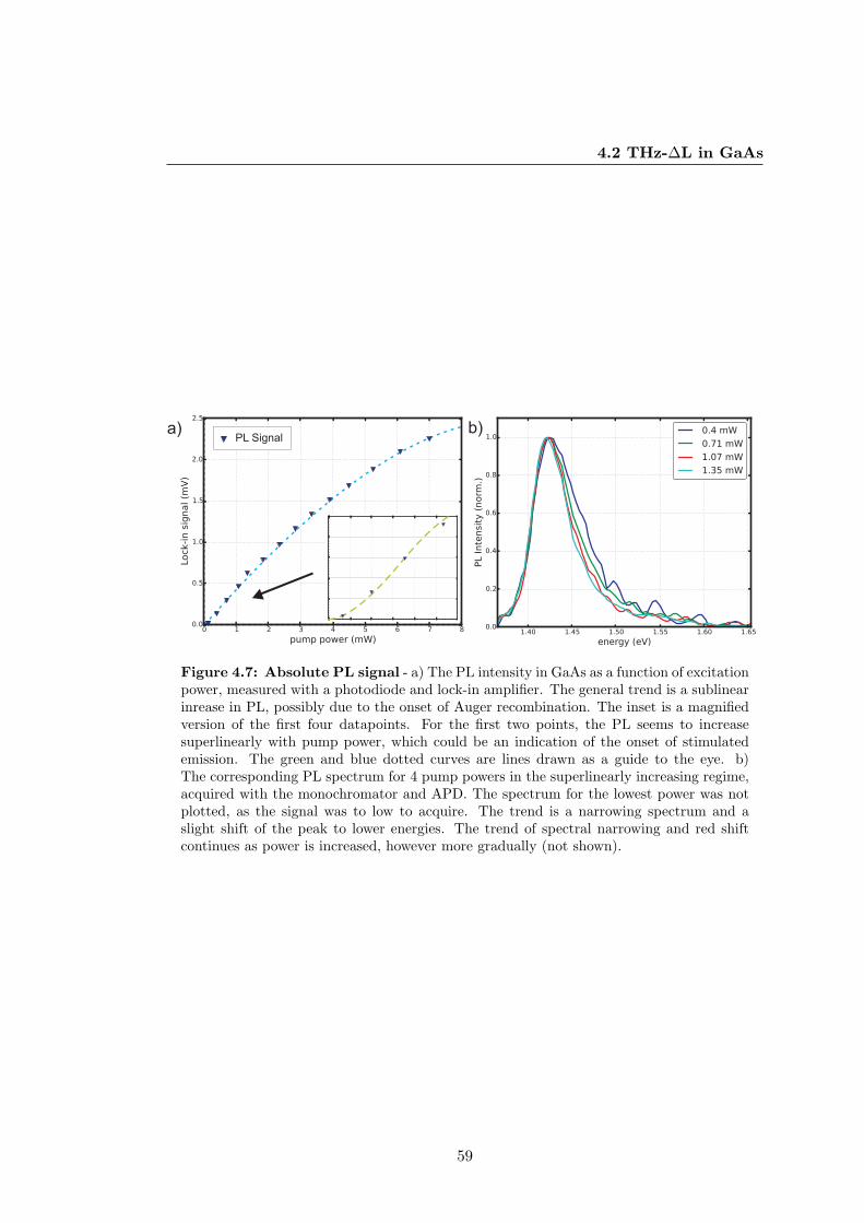
4.2 THz-∆L in GaAs
a) b)PL Signal
Figure 4.7: Absolute PL signal - a) The PL intensity in GaAs as a function of excitationpower, measured with a photodiode and lock-in amplifier. The general trend is a sublinearinrease in PL, possibly due to the onset of Auger recombination. The inset is a magnifiedversion of the first four datapoints. For the first two points, the PL seems to increasesuperlinearly with pump power, which could be an indication of the onset of stimulatedemission. The green and blue dotted curves are lines drawn as a guide to the eye. b)The corresponding PL spectrum for 4 pump powers in the superlinearly increasing regime,acquired with the monochromator and APD. The spectrum for the lowest power was notplotted, as the signal was to low to acquire. The trend is a narrowing spectrum and aslight shift of the peak to lower energies. The trend of spectral narrowing and red shiftcontinues as power is increased, however more gradually (not shown).
59

4. THZ MODULATION OF PHOTOLUMINESCENCE
4.2.3 High Fluence Regime
At high pump powers a qualitatively new feature develops. The integrated THz-∆PL
as a function of time delay shows PLE when the THz pulse arrives before the optical
pulse, as seen in fig. 4.8. In this long baseline scan, there are three separate compo-
nents to the THz-∆PL, 1) the main peak, when the THz pulse and optical pulse are
incident on the semiconductor at the same time, 2) when the THz pulse reflected from
the back surface reaches the front surface simultaneously to the optical pulse, and 4) off
t0 behaviour when neither the incident, nor back surface reflected pulses are coincident
with the optical pulse. This scan was taken at 1.5 mW .
It is curious to note that the amplitude of THz-PLQ from the backsurface reflected
pulse is almost as large as that of the front surface. It is unexpected as the electric
field of the THz pulse is significantly reduced after reflection from the back surface.
This behaviour, where stronger nonlinear effects are seen with back surface illumina-
tion, has been seen before in studies of THz induced transient voltage pulses in doped
semiconductors(62), as well as in studies of THz-induced photoemission from plasmonic
antennae(79).
In fig. 4.8, wafer stacks were used to separate the backreflection further in time from
the main pulse. At the moment, there is no clear interpretation of the off t0 effects.
The high quality of the wafer, indicated by the low intrinsic carrier concentration, could
mean that some carriers excited from the previous photoexcitation pulse have diffused
into the bulk and have not recombined(80). This could be some sort of interaction
between photoexcited carriers left over from the previous pulse.
The THz-∆PL also becomes strongly dependent on the compressor setting of the
excitation pulse. Shown in fig. 4.9 is the integrated THz-∆PL near t0 for 3 different
compressor settings with the direction of the chirp indicated by the inset. When this
dataset was taken, there was also no method in place to quantitatively measure the
amount of pulse chirp. 4.9 a), b), and c), correspond to compressor settings which gave
approximately 50% of the maximum SHG, maximum SHG, and 50% of the maximum
60

4.2 THz-∆L in GaAs
backsurface reflection
main peak
off t behaviour0
Figure 4.8: Long Baseline Scan - THz-∆PL in GaAs at 1.5 mW. The peak at 0 ps ist0 for the incident pulse while the peak at -25 ps is t0 for the back surface reflection. Thereis also an element of off-t0 integrated enhancement.
but with the opposite chirp, respectively.
All three curves in fig. 4.9 show a positive offset, integrated THz-PLE, at negative
time due to the off t0 effects. In the chirped pulse cases, there is strong integrated PLE
near t0. In other datasets, there was indications that the behaviour was asymmetric
about the minimum pulse duration. This could be due to the cubic phase of the exci-
tation pulse as discussed in chapter 2.
61
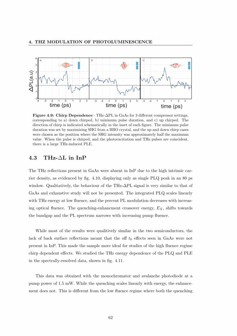
4. THZ MODULATION OF PHOTOLUMINESCENCE
b) c)a)
time (ps) time (ps) time (ps)
PL(a
.u)
-4 -3 -2 -1 0 1 2 3
4
3
2
1
0
-1
-2-3 -2 -1 0 1 2 3 -3 -2 -1 0 1 2 3
Figure 4.9: Chirp Dependence - THz-∆PL in GaAs for 3 different compressor settings,corresponding to a) down chirped, b) minimum pulse duration, and c) up chirped. Thedirection of chirp is indicated schematically in the inset of each figure. The minimum pulseduration was set by maximizing SHG from a BBO crystal, and the up and down chirp caseswere chosen as the position where the SHG intensity was approximately half the maximumvalue. When the pulse is chirped, and the photoexcitation and THz pulses are coincident,there is a large THz-induced PLE.
4.3 THz-∆L in InP
The THz reflections present in GaAs were absent in InP due to the high intrinsic car-
rier density, as evidenced by fig. 4.10, displaying only as single PLQ peak in an 80 ps
window. Qualitatively, the behaviour of the THz-∆PL signal is very similar to that of
GaAs and exhaustive study will not be presented. The integrated PLQ scales linearly
with THz energy at low fluence, and the percent PL modulation decreases with increas-
ing optical fluence. The quenching-enhancment crossover energy, EX , shifts towards
the bandgap and the PL spectrum narrows with increasing pump fluence.
While most of the results were qualitively similar in the two semiconductors, the
lack of back surface reflections meant that the off t0 effects seen in GaAs were not
present in InP. This made the sample more ideal for studies of the high fluence regime
chirp dependent effects. We studied the THz energy dependence of the PLQ and PLE
in the spectrally-resolved data, shown in fig. 4.11.
This data was obtained with the monochromator and avalanche photodiode at a
pump power of 1.5 mW. While the quenching scales linearly with energy, the enhance-
ment does not. This is different from the low fluence regime where both the quenching
62

4.3 THz-∆L in InP
Figure 4.10: THz-∆PL in InP - A long baseline integrated THz-PLQ scan in InP.The80 ps window shows a lack of reflections, making this sample more ideal for the study ofTHz-∆PL in the high fluence regime.
and enhancement scale linearly.
In the high fluence regime, the THz-∆PL shows a dependence on laser pulse com-
pressor setting, as shown in fig. 4.12. Interestingly, as the amount of chirp is increased
the integrated behaviour shows both PLQ and PLE in the same time delay scan. It
appears as though when the optical pulse is coincident with the leading peak of the
THz pulse there is PLQ, while when it is coincident with the trailing half of the THz
pulse there is PLE 4.12.
We also studied the spectrally-resolved ∆PL for each of the three compressor set-
tings from fig. 4.12. The results are shown in fig. 4.13. Here, it was difficult to make
a proper comparison between the three spectrally resolved datasets as changing the
63
4. THZ MODULATION OF PHOTOLUMINESCENCE
compressor setting changed the stage position of t0. The stage position was chosen as
the location with the maximum amplitude of integrated PLQ. The blue, green, and
red curves correspond to figs. 4.12 a) to c) respectively. By changing the compressor
setting, the lineshape of the differential PL is changed.
64

4.3 THz-∆L in InP
Figure 4.11: Spectra THz Energy dependence - Total PLE (green) and PLQ (red)in InP at 3.0 mW pump power, obtained by integrating over the positive (enhancement)and negative (quenching) regions in the spectrally-resolved data, as a function of THz pulseenergy. The integrated PLQ seems to scale linearly with THz energy as indicated by thelinear fit, while the enhancement shows nonlinear behaviour. The green line is drawn as aguide to the eye, to highlight the sub linearity of the trend. Here data was collected withan avalanche photodiode and monochromator, and scans were averaged until the traceconverged.
65

4. THZ MODULATION OF PHOTOLUMINESCENCE
a) b) c)
time (ps) time (ps) time (ps)
-4 -3 -2 -1 0 1 2 3 -3 -2 -1 0 1 2 3 -3 -2 -1 0 1 2 3
2
0
-2
-4
-6
-8
-10
PL(a
.u)
Figure 4.12: Integrated Chirp Dependence - The integrated THz-∆PL in InP forthree different compressor settings at 3.0 mW pump power. a) Minimum pulse duration setby maximizing SHG in a thin BBO crystal, b) a small amount of down chirp correspondingto 50% of the maximum SHG, c) a large down chirp correpsonding to approximately 25%of the maximum SHG. The direction of chirp is indicated schematically in the inset.
66

4.3 THz-∆L in InP
1.25 1.30 1.35 1.40 1.45 1.50 1.55
energy (eV)
−3
−2
−1
0
1
2
3
∆PL
(lock-in signal)
Miniumum Duration
Small Downchirp
Large Downchirp
Figure 4.13: Spectrally-Resolved Chirp Dependence - Spectrally resolved THz-∆PL in InP at 3.0 mW pump power for three different compressor settings. The lineshapechanges dramatically for each case. Here, the compressor settings were chosen as thelocations where SHG was maximized, half maximum, and one quarter maximum for theminimum, small downchirp, and large downchirp cases
67

Chapter 5
Discussion
We have shown that intense THz pulses modulate both the luminescence intensity and
lineshape in the direct-gap semiconductors GaAs and InP. A wide range of excitation
conditions have been explored and in general it is seen that THz pulses enhance high
energy PL and quench near gap PL. In almost all conditions quenching dominates.
However, with high density excitation and chirped optical pulses the enhancement can
overwhelm the quenching.
Several reports of intense THz pulse effects on luminescence exist in a variety of
systems. Shinokita et al. showed THz-PLE in undoped GaAs quantum wells under
CW excitation, and attributed it to ionization of trap states at interfaces(81). Also in
quantum wells, Rice et al. observed transient quenching of excitonic luminescence in
quantum wells with THz pulses tuned to the the 1s-2p excitonic transition(82). Inter-
estingly, they also saw simultaneous enhancement of 2s luminescence, from Coulomb
mediated transitions from the 2p to 2s states. In bulk GaAs, metamaterial enhanced
THz fields on the order of tens of MV/cm have been shown to induce interband Zener
tunneling, resulting in luminescence(15). However, none of these results can be used
to explain the THz modulation of luminescence presented here. The first and the third
both exhibit complex electric field dependence which is different from the linearity
observed here. The second requires the presence of an exciton population, which is
unlikley at high temperatures.
68
In another context, researchers have explored the THz-pulse-induced Franz-Keldysh
effect, which is the modification of the semiconductor absorption coefficient by an elec-
tric field. In these experiments, the time delay data showed similar behaviour to the
THz-∆PL. Here again, however, a complicated electric field dependence is expected(83).
The linearity with increasing THz energy of the integrated PLQ, as well as the unmodi-
fied lineshape of the differential spectrum indicate that the THz-∆PL we have observed
is not an obvious manifestation of the Franz-Keldysh effect.
THz-PLQ has been studied before by Liu et al. and attributed to carrier heating,
however no model was presented, and no THz-PLE was observed(67). Chu et al. devel-
oped a model to simulate the THz-PLQ using Monte Carlo simulations(68). Here, the
interpretation of the effect is that intervalley phonons emitted due to carrier accelera-
tion in the THz field act to enhance non-radiative recombination. Within this model,
it is not clear whether intervalley phonons act as non-radiative centers themselves, or
if they act to increase transition rates through the usual channels. The latter seems
possible, as molecular dynamics simulations have shown that high-wavevector phonons
couple more efficiently to lattice defects(84) and heat non-radiative centers.
In our results we have seen up to 2% reduction in PL in GaAs, and Liu et al. quote
up to 17% in CdTe(67). In their model, Chu et al. assume that all modulation of
luminescence occurs during the lifetime of the non-equilibrium phonons, which is just
2.5 ps for GaAs. A back of the envelope calcuation assuming an exponential decay
puts the required rate of non-radiative recombination on the order of nanoseconds. For
typical non-radiative centers trapping can occur on picosecond timescales(85), while
emptying typically occurs on microsecond timescales(86).
While not entirely unreasonable, it is difficult to reconcile the large modulation of
luminescence reported. It is useful to consider the indirect gap semiconductors ger-
manium and silicon for comparison. The conduction band minimum for germanium
(silicon) is at the L (X) point, where there are 4 (3) inequivalent minima. As a re-
sult, intervalley scattering can occur near the bottom of the conduction band, and it
is the dominant relaxation mechanism during optical excitation. However, nanosecond
69

5. DISCUSSION
recombination times are not observed in these systems.
This evidence is not entirely convincing, and it is possible that this relaxation
channel requires a non-equilibrium phonon population. The configurational coordinate
diagrams introduced in chapter 2, and used to understand non-radiative recombination,
is a highly simplified model. It is possible that the high effective temperatures of in-
tervalley phonons open up new, efficient, channels for recombination. The hot phonon
mechanism can also result in long lived non-equilibrium phonon. Hot phonons would
also help explain the enhancement of high energy luminescence as phonon reabsorption
keeps the electron distribution hot longer, and releasing more high energy PL.
One point which will be difficult to understand with this model is the fast switching
time, i.e, there is essentially no modulation of luminescence with |∆t| < 1 ps. From
previous studies, it is known that intense THz pulses can cause intervalley scattering
long after t0, at densities higher than 1018 cm−3(65). In this case, it is not obvious why
quenching does not occur at larger time delays.
Several interesting phenomenon occur at early times which could explain this be-
haviour. Ultrafast current surges due to built in surface fields, or current surge due
to the difference between electron and hole effective masses (the photo-dember effect)
result in charge separation(38, 39), which is known to reduce radiative efficiency. The
strong electric field of the THz pulse leads to charge separation parallel to the surface,
although it only lasts for several picoseconds(62). This transient charge separation
alone is unlikely to account for the observed magnitude of quenching.
Alternatively, the THz-PLQ could be due to intervalley-scattering induced suppres-
sion of diffusion into the bulk during the initial current surge. This could hold carriers
near surface where there is a high density of non-radiative states, increasing the rate
of nonradiative recombination. It is possible to test this by chemically passivating the
semiconductor surface, which significantly reduces the trap density(80), and should re-
duce the amount of luminescence quenching within this model.
70

Shifting focus, results with increasing excitation density point to the onset of stimu-
lated emission in the PL spectrum. At liquid nitrogen temperature, stimulated emission
results in rapid carrier density depletion by a factor of ten in just 20 picoseconds, at
a carrier density of only 1.5×1018 cm−3(87). While stimulated emission is suppressed
at room temperature, there is likely still some contribution. It should be noted that
even if the regime of optical gain is not reached, stimulated emission still results in an
increased rate of recombination, enhancing radiative efficiency.
It is possible that THz pulse induced intervalley scattering could be suppressing
stimulated emission by reducing Γ-valley population. In support of this conclusion, re-
ports of sub-picosecond resolution luminescence studies in GaAs have shown a rise time
of 10 ps when carriers are excited above the intervalley scattering threshold(88). By
delaying light emission, the peak intensities required for stimulated emission to occur
may not be reached, nulling the enhanced radiative efficiency which comes along with
stimulated emission.
In general, the rate of stimulated emission depends on the elecron and hole quasi-
Fermi levels, and the temperature(77), with lower temperature and higher Fermi levels
resulting in more stimulated emission. The initial hot carrier temperature is dependent
on the excess energy on excitation(78), so a lower initial temperature is expected for
CdTe, vs GaAs, vs InP. This correlates well with the observed ratios of luminescence
quenching, with CdTe being the highest reported, and InP the lowest as we have ob-
served.
Still, based on our current results there is no smoking gun evidence pointing to
the correct mechanism. From an experimental perspective, it would be interesting
to explore the low fluence regime and low temperatures. If the THz-PLQ is due to
suppression of stimulated emission, there would be no modulation at low fluence, and
alternatively very large modulation at low temperatures. The low fluence regime should
also shed light on the phonon-defect coupling model of Chu et al. as at low enough
excitation fluences intense THz pulses will induce intervalley scattering long after t0,
which should manifest in the time delay data.
71
5. DISCUSSION
To extend these interpretations to the high fluence and chirped-pulse regime may
be difficult. The quasi-Fermi level calculated from linear absorption is approaching the
level of excess energy on excitation, and nonlinear absorption due to the Burrsein-Moss
shift is important(89). Pulse compression begins to effect absorption and the distribu-
tion of carriers as a function of depth is different from that of linear absorption(90).
Additionally, Auger decay begins to dominate the recombination dynamics at car-
rier densities above 1019 cm−3(76). Here, it is possible that the reduction of density
in the Γ-valley due to intervalley scattering reduces the rate of Auger recombination.
An accurate model of initial carrier distribution, including nonlinear absorption, dif-
fusion, and surface trapping, is likely required to understand these effects. As well,
the compressor dependence of our results highlights the need for more accurate laser
characterization, as discussed in chap. 2.
In this discussion, we have also ignored other interesting phenomenon which occur
during the initial stages of excitation and relaxation. At low temperatures, unnexpected
excitonic enhancement was seen in quantum wells during the first few picoseconds after
exctiation(10). Some quantum-kinetic effects are important even at room temperature.
When an electron-hole plasma is generated, a plasmon like response does not develop
immediately and the couloumb interaction is unscreened. A fully correlated system
forms on timescales of the inverse plasma frequency, in our case on the order of hun-
dreds of femtoseconds for carrier densities on the order of 1018 cm−3(9).
Simultaneously, coherent phonons are excited by impulsive excitation(91). Very lit-
tle work has been done studying the simultaneous coherent evolution of both the lattice
and carriers. Recent work using time-and-angle-resolved photoemission spectroscopy
have pointed towards novel physical processes which occur during the initial thermal-
ization phase(92). Perhaps non-radiative recombination channels which are affected
by the THz pulse are present in this regime. While without precedent, these exciting
possibilities are worth considering, as they could point towards new physics.
Here we have presented a study of these effects for a wide range of conditions. We
have suggested several new avenues to explore experimentally, including temperature
72

dependence, low excitation density, and, surface passivation. These studies will likely
shed light on the mechanism of THz-PLQ in the low fluence regime. To understand the
high fluence regime, modelling will be required due to nonlinear absorption and effects
extreme carrier densities.
73
Chapter 6
Conclusion
Despite having been a major research focus for decades, new work on semiconductors
such as GaAs and InP is still leading to new physics. While theories exist which are
formally exact, complexity limits their predicatability and experiment is required as a
guide. With the development of new tools, qualitatively new information can lead to
new insight.
In the last several years, the technique of tilted-pulse-front optical rectification in
lithium niobate has brought THz nonlinear optics to the optics bench. With our lithium
niobate source, we have achieved peak electric fields of 230 kV/cm. This source has
been used to study nonlinearities of transient states in semiconductors.
We have studied how these pulses can modulate photoluminescence in GaAs and
InP. Modulation only occurs when the photoexcitation and THz pulse are simultane-
ously incident on the crystal. When transform limited photoexcitation pulses are used,
PLQ is observed near the bandgap, PLE is observed for hot carriers at all carrier den-
sities. However, quenching dominates, and there is an overall reduction in intensity.
We have discussed several possible mechanisms for the THz modulation of lumi-
nescence, 1) non-radiative recombination due to intervalley phonons, 2) suppressed
diffusion into the substrate, enhancing surface recombination, due to intervalley scat-
tering, and, 3) suppression of stimulated emission by intervalley scattering. Exploration
of the low carrier density and low temperature regimes will shed light on which of these
74

mechanisms is the correct interpretation.
The intervalley phonon enhanced non-radiative recombination would be of interest
to device engineers, and clarification is needed as to whether this occurs. Alternatively,
the second mechanism, the enhancement of surface recombination, also needs clarifi-
cation. The physics of interfaces is an important field in itself, and much of modern
materials science is based on the devlopement of functionalized surfaces. This mecha-
nism would represent a new tool to control optically excited distributions in real space,
potentially acting as a unique probe of interface physics.
Perhaps the most interesting possibility would be if suppression of stimulated emis-
sion is the origin. Exploration of these effects at low temperature, could yield interesting
results. The ability to modulate stimulated emission on picosecond timescales would
present unique technological applications, and point to a broad range of novel systems
to study THz modulation of luminescence.
The high excitation density results are still puzzling. Adjustment of the laser pulse
compressor can result in integrated luminescence enhancement, and modification of the
luminescence spectrum. It is unclear how any of the previously discussed models can
explain the results in this regime. This behaviour may be difficult to understand, due
to the extreme pump fluences, but better laser pulse characterization will be required
to understand this regime.
As part of the bigger picture, this work fits in a community which aims to understand
the nature of light-matter interactions from a fundamental level. Over the last several
decades, the development of new technologies has resulted in a continually shifting
paradigm of light-matter interactions, especially in the regime just picoseconds after
photoexcitation. Intense THz pulse sources represent one such technology, helping to
add new pieces to the puzzle. This work will help clarify our understanding of the
ultrafast interactions which occur immediately after photoexcitation.
75

References
[1] T. H. Maiman. Stimulated Optical Radiation in Ruby. Nature,
187(4736):493–494, 1960. [pg. 2]
[2] P. A. Franken, A. E. Hill, C. W. Peters, and G. Weinreich. Generation
of Optical Harmonics. Phys. Rev. Lett., 7:118–119, Aug 1961. [pg. 2]
[3] S. Backus, Charles G. Durfee III, M. M. Murnane, and H. C. Kapteyn.
High power ultrafast lasers. Review of Scientific Instruments, 69(3):1207–
1223, 1998. [pg. 2]
[4] T. J. Hammond, G. G. Brown, K. Taec Kim, D. M. Villeneuve, and P. B.
Corkum. Attosecond pulses measured from the attosecond lighthouse.
Nat. Photon., 10(3):171–175, Mar 2016. Letter. [pg. 2]
[5] F. H. Su, F. Blanchard, G. Sharma, L. Razzari, A. Ayesheshim, T. L.
Cocker, L. V. Titova, T. Ozaki, J.-C. Kieffer, R. Morandotti, M. Reid,
and F. A. Hegmann. Terahertz pulse induced intervalley scattering in
photoexcited GaAs. Optics Express, 17(12):9620, 2009. [pg. 2]
[6] P. U. Jepsen, D. G. Cooke, and M. Koch. Terahertz spectroscopy and
imaging Modern techniques and applications. Laser & Photonics Reviews,
5(1):124–166, 2011. [pg. 3]
[7] S. Keiber, S. Sederberg, A. Schwarz, M. Trubetskov, V. Pervak,
F. Krausz, and N. Karpowicz. Electro-optic sampling of near-infrared
waveforms. Nature Photonics, 10(3):159–162, 2016. [pg. 3]
76

REFERENCES
[8] M. C. Nuss, D. H. Auston, and F. Capasso. Direct Subpicosecond Mea-
surement of Carrier Mobility of Photoexcited Electrons in Gallium Ar-
senide. Physical Review Letters, 58(22):2355–2358, 1987. [pg. 3]
[9] R. Huber, F. Tauser, A. Brodschelm, M. Bichler, G. Abstreiter, and
A. Leitenstorfer. How many-particle interactions develop after ultra-
fast excitation of an electronhole plasma. Nature, 414(6861):286–289, 2001.
[pg. 3, 72]
[10] R. A. Kaindl, M. A. Carnahan, D. Hagele, R. Lovenich, and D. S.
Chemla. Ultrafast terahertz probes of transient conducting and insu-
lating phases in an electronhole gas. Nature, 423(6941):734–738, 2003. [pg.
4, 19, 72]
[11] O. Schubert, M. Hohenleutner, F. Langer, B. Urbanek, C. Lange,
U. Huttner, D. Golde, T. Meier, M. Kira, S. W. Koch, and R. Huber.
Sub-cycle control of terahertz high-harmonic generation by dynamical
Bloch oscillations. Nature Photonics, 8(2):119–123, 2014. [pg. 4]
[12] K.-L. Yeh, M. C. Hoffmann, J. Hebling, and Keith A. Nelson. Genera-
tion of 10µJ ultrashort terahertz pulses by optical rectification. Applied
Physics Letters, 90(17):171121, 2007. [pg. 4, 33]
[13] L. Razzari, F. H. Su, G. Sharma, F. Blanchard, A. Ayesheshim, H.-C.
Bandulet, R. Morandotti, J.-C. Kieffer, T. Ozaki, M. Reid, and F. A.
Hegmann. Nonlinear ultrafast modulation of the optical absorption of
intense few-cycle terahertz pulses in n -doped semiconductors. Physical
Review B, 79(19):193204, 2009. [pg. 4, 22]
[14] T. Kampfrath, A. Sell, G. Klatt, A. Pashkin, S. Mahrlein, T. Dekorsy,
M. Wolf, M. Fiebig, A. Leitenstorfer, and R. Huber. Coherent tera-
hertz control of antiferromagnetic spin waves. Nature Photonics, 5(1):31–34,
2011. [pg. 4]
[15] C. Lange, T. Maag, M. Hohenleutner, S. Baierl, O. Schubert,
E.R.J. Edwards, D. Bougeard, G. Woltersdorf, and R. Huber. Ex-
tremely Nonperturbative Nonlinearities in GaAs Driven by Atomically
77

REFERENCES
Strong Terahertz Fields in Gold Metamaterials. Physical Review Letters,
113(22):227401, 2014. [pg. 4, 44, 68]
[16] T. Kampfrath, K. Tanaka, and K. A. Nelson. Resonant and nonreso-
nant control over matter and light by intense terahertz transients. Nature
Photonics, 7(9):680–690, 2013. [pg. 4]
[17] Charles Kittel. Introduction to Solid State Physics. John Wiley & Sons, Inc.,
New York, 6th edition, 1986. [pg. 9]
[18] Robert W. Boyd. Nonlinear Optics, Third Edition. Academic Press, 3rd edition,
2008. [pg. 9]
[19] E. Wigner and F. Seitz. On the Constitution of Metallic Sodium. Physical
Review, 43(10):804–810, 1933. [pg. 10]
[20] I. Saıdi, S. Ben Radhia, and K. Boujdaria. Band parameters of GaAs,
InAs, InP, and InSb in the 40-band kp model. Journal of Applied Physics,
107(4):043701, 2010. [pg. 10, 50]
[21] Timothy B. Boykin, Gerhard Klimeck, R. Chris Bowen, and Fabiano
Oyafuso. Diagonal parameter shifts due to nearest-neighbor displace-
ments in empirical tight-binding theory. Phys. Rev. B, 66:125207, Sep 2002.
[pg. 10]
[22] A. De and C. E. Pryor. Predicted band structures of III-V semicon-
ductors in the wurtzite phase. Physical Review B, 81(15):155210, 2010. [pg.
10]
[23] I. Vurgaftman, J. R. Meyer, and L. R. Ram-Mohan. Band parameters
for IIIV compound semiconductors and their alloys. Journal of Applied
Physics, 89(11):5815–5875, 2001. [pg. 12]
[24] P. Wurfel. The chemical potential of radiation. Journal of Physics C:
Solid State Physics, 15(18):3967, 1982. [pg. 14]
[25] D. S. Kim and P. Y. Yu. Phonon temperature overshoot in GaAs excited
by subpicosecond laser pulses. Physical Review Letters, 64(8):946–949, 1990.
[pg. 14, 51]
78

REFERENCES
[26] I. Pelant and J. Valenta. Luminescence Spectroscopy of Semiconductors. Lu-
minescence Spectroscopy of Semiconductors. OUP Oxford, 2012. [pg. 15]
[27] W. Shockley and W. T. Read Jr. Statistics of the Recombinations of
Holes and Electrons. Physical Review, 87(5):835–842, 1952. [pg. 15]
[28] Mark Lundstrom. Fundamentals of Carrier Transport. Cambridge University
Press, 2009. [pg. 17]
[29] S. Hunsche, H. Heesel, A. Ewertz, H. Kurz, and J. H. Collet. Spectral-
hole burning and carrier thermalization in GaAs at room temperature.
Physical Review B, 48(24):17818, 1993. [pg. 18]
[30] M Feneberg, S. Osterburg, K. Lange, C. Lidig, B. Garke, R. Goldhahn,
E. Richter, C. Netzel, M. D. Neumann, N. Esser, S. Fritze, H. Witte,
J. Blasing, A. Dadgar, and A. Krost. Band gap renormalization and
Burstein-Moss effect in silicon- and germanium-doped wurtzite GaN up
to 1020 cm3. Physical Review B, 90(7):075203, 2014. [pg. 18]
[31] A. Leitenstorfer, T. Elsaesser, F. Rossi, T. Kuhn, W. Klein, G. Boehm,
G. Traenkle, and G. Weimann. Coherent optical generation of nonequi-
librium electrons studied via band-to-acceptor luminescence in GaAs.
Physical Review B, 53(15):9876, 1996. [pg. 19, 53]
[32] Mark Fox. Optical properties of solids, 3. Oxford university press, 2010. [pg.
19, 51]
[33] Mackillo Kira and Stephan W. Koch. Semiconductor Quantum Optics.
Cambridge University Press, 2011. [pg. 19]
[34] J. Sjakste, N. Vast, M. Calandra, and F. Mauri. Wannier interpolation
of the electron-phonon matrix elements in polar semiconductors: Polar-
optical coupling in GaAs. Physical Review B, 92(5):054307, 2015. [pg. 20]
[35] M. Bernardi, D. Vigil-Fowler, C. S. Ong, J. B. Neaton, and S. G.
Louie. Ab initio study of hot electrons in GaAs. Proceedings of the National
Academy of Sciences of the United States of America, 112(17):5291–5296, 2015.
[pg. 20]
79

REFERENCES
[36] J. A. Kash, J. C. Tsang, and J. M. Hvam. Subpicosecond time-resolved
Raman spectroscopy of LO phonons in GaAs. Physical review letters,
54(19):2151, 1985. [pg. 20]
[37] A. Leitenstorfer, S. Hunsche, J. Shah, M. C. Nuss, and W. H. Knox.
Femtosecond high-field transport in compound semiconductors. Physical
Review B, 61(24):16642–16652, 2000. [pg. 22, 53]
[38] G. Klatt, F. Hilser, W. Qiao, M. Beck, R. Gebs, A. Bartels, K. Huska,
U. Lemmer, G. Bastian, M.B. Johnston, M. Fischer, J. Faist, and
T. Dekorsy. Terahertz emission from lateral photo-Dember currents.
Optics Express, 18(5):4939, 2010. [pg. 22, 70]
[39] M. Reid, I. V. Cravetchi, and R. Fedosejevs. Terahertz radiation and
second-harmonic generation from InAs: Bulk versus surface electric-
field-induced contributions. Physical Review B, 72(3):035201, 2005. [pg. 22,
70]
[40] M. C. Beard, G. M. Turner, and C. A. Schmuttenmaer. Transient pho-
toconductivity in GaAs as measured by time-resolved terahertz spec-
troscopy. Physical Review B, 62(23):15764, 2000. [pg. 23]
[41] M. Beaudoin, A. J. G. DeVries, S. R. Johnson, H. Laman, and T. Tiedje.
Optical absorption edge of semi-insulating GaAs and InP at high tem-
peratures. Applied physics letters, 70(26):3540–3542, 1997. [pg. 25]
[42] J. K. Katahara and H. W. Hillhouse. Quasi-Fermi level splitting and
sub-bandgap absorptivity from semiconductor photoluminescence. Jour-
nal of Applied Physics, 116(17):173504, 2014. [pg. 25]
[43] J. H. Collet, W. W. Ruhle, M. Pugnet, K. Leo, and A. Million.
Electron-hole plasma dynamics in CdTe in the picosecond regime. Phys.
Rev. B, 40(18):12296–12303, Dec 1989. [pg. 25, 51]
[44] T. Brabec, Ch. Spielmann, P. F. Curley, and F. Krausz. Kerr lens
mode locking. Optics Letters, 17(18):1292, 1992. [pg. 28]
80
REFERENCES
[45] A. M. Dunlop, W. J. Firth, and E. M. Wright. Master equation for
spatio-temporal beam propagation and Kerr lens mode-locking. Optics
Communications, 138(1):211–226, 1997. [pg. 28]
[46] B. Proctor, E. Westwig, and F. Wise. Characterization of a Kerr-lens
mode-locked Ti:sapphire laser with positive group-velocity dispersion.
Optics Letters, 18(19):1654, 1993. [pg. 28]
[47] Liu Hua-Gang, Hu Ming-Lie, Song You-Jian, Li Yan-Feng, Chai Lu, and
Wang Ching-Yue. Operation of Kerr-lens mode-locked Ti:sapphire laser
in the non-soliton regime. Chinese Physics B, 19(1):014215–6, 2010. [pg. 28]
[48] J. V. Rudd, G. Korn, S. Kane, J. Squier, G. Mourou, and P. Bado.
Chirped-pulse amplification of 55-fs pulses at a 1-kHz repetition rate in
a Ti:Al 2O 3 regenerative amplifier. Optics Letters, 18(23):2044, 1993. [pg.
28]
[49] Andrew Marc Weiner. Ultrafast optics. Wiley series in pure and applied optics.
Wiley, 2009. [pg. 31]
[50] Rick Trebino, Kenneth W. DeLong, David N. Fittinghoff, John N.
Sweetser, Marco A. Krumbugel, Bruce A. Richman, and Daniel J.
Kane. Measuring ultrashort laser pulses in the time-frequency domain
using frequency-resolved optical gating. Review of Scientific Instruments,
68(9):3277–3295, 1997. [pg. 31]
[51] Daniel J. Kane. Principal components generalized projections: a review
[Invited]. JOSA B, 25(6):A120–A132, 2008. [pg. 32]
[52] Patrick O’Shea, Mark Kimmel, Xun Gu, and Rick Trebino. Highly sim-
plified device for ultrashort-pulse measurement. Optics Letters, 26(12):932,
2001. [pg. 32]
[53] Masaya Nagai, Mukesh Jewariya, Yuki Ichikawa, Hideyuki Ohtake,
Toshiharu Sugiura, Yuzuru Uehara, and Koichiro Tanaka. Broadband
and high power terahertz pulse generation beyond excitation band-
width limitation via χ(2) cascaded processes in LiNbO3. Optics Express,
17(14):11543, 2009. [pg. 33, 41]
81
REFERENCES
[54] Koustuban Ravi, Wenqian Ronny Huang, Sergio Carbajo, Emilio A.
Nanni, Damian N. Schimpf, Erich P. Ippen, and Franz. X. Kartner. The-
ory of terahertz generation by optical rectification using tilted-pulse-
fronts. Optics Express, 23(4):5253, 2015. [pg. 33, 41]
[55] J. A. Fulop, L. Palfalvi, G. Almasi, and J. Hebling. Design of high-
energy terahertz sources based on optical rectification. Optics Express,
18(12):12311, 2010. [pg. 33, 35]
[56] Michael I. Bakunov and Sergey B. Bodrov. Terahertz generation with
tilted-front laser pulses in a contact-grating scheme. Journal of the Optical
Society of America B, 31(11):2549, 2014. [pg. 33]
[57] T. E. Stevens, J. K. Wahlstrand, J. Kuhl, and R. Merlin. Cherenkov
Radiation at Speeds Below the Light Threshold: Phonon-Assisted
Phase Matching. Science, 291(5504):627–630, 2001. [pg. 34]
[58] Maksim Kunitski, Martin Richter, Mark D. Thomson, Arno Vreden-
borg, Jian Wu, Till Jahnke, Markus Schoffler, Horst Schmidt-Bock-
ing, Hartmut G. Roskos, and Reinhard Dorner. Optimization of single-
cycle terahertz generation in LiNbO 3 for sub-50 femtosecond pump
pulses. Optics Express, 21(6):6826, 2013. [pg. 35]
[59] H. Hirori, A. Doi, F. Blanchard, and K. Tanaka. Single-cycle tera-
hertz pulses with amplitudes exceeding 1 MV/cm generated by optical
rectification in LiNbO3. Applied Physics Letters, 98(9):091106, 2011. [pg. 35,
37]
[60] I.z. Kozma, G. Almsi, and J. Hebling. Geometrical optical modeling of
femtosecond setups having angular dispersion. Applied Physics B: Lasers
& Optics, 76(3):257, 2003. [pg. 35]
[61] Zhenyou Wang. Ultrafast imaging of terahertz waves. PhD thesis, University of
Alberta, 2013. [pg. 36]
[62] A. K. Ayesheshim. High-power Terahertz Pulse Generation and Nonlinear Ter-
ahertz Carrier Dynamics in Semiconductors. PhD thesis, University of Alberta,
2015. [pg. 37, 60, 70]
82

REFERENCES
[63] Yun-Shik Lee. Principles of Terahertz Science and Technology. Springer Pub-
lishing Company, Incorporated, 1st edition, 2008. [pg. 37]
[64] F. Blanchard, X. Ropagnol, H. Hafez, H. Razavipour, M. Bolduc,
R. Morandotti, T. Ozaki, and D. G. Cooke. Effect of extreme pump
pulse reshaping on intense terahertz emission in lithium niobate at mul-
timilliJoule pump energies. Optics Letters, 39(15):4333, 2014. [pg. 41]
[65] G. Sharma, I. Al-Naib, H. Hafez, R. Morandotti, D. G. Cooke, and
T. Ozaki. Carrier density dependence of the nonlinear absorption of
intense THz radiation in GaAs. Optics Express, 20(16):18016, 2012. [pg. 43,
70]
[66] Martin van Exter, Ch. Fattinger, and D. Grischkowsky. Terahertz
time-domain spectroscopy of water vapor. Optics Letters, 14(20):1128, 1989.
[pg. 44]
[67] Jingle Liu, Gurpreet Kaur, and X.-C. Zhang. Photoluminescence
quenching dynamics in cadmium telluride and gallium arsenide induced
by ultrashort terahertz pulse. Applied Physics Letters, 97(11):111103, 2010.
[pg. 48, 49, 55, 69]
[68] Zheng Chu, Jinsong Liu, and Jingle Liu. Study of THz-wave-induced
photoluminescence quenching in GaAs and CdTe. Applied Physics B,
109(1):113–119, 2012. [pg. 48, 69]
[69] D. J. Ashen, P. J. Dean, D. T. J. Hurle, J. B. Mullin, A. M. White, and
P. D. Greene. The incorporation and characterisation of acceptors in
epitaxial GaAs. Journal of Physics and Chemistry of Solids, 36(10):1041–1053,
1975. [pg. 51]
[70] Bruno Ullrich, Akhilesh K. Singh, Puspendu Barik, Haowen Xi, and
Mithun Bhowmick. Inherent photoluminescence Stokes shift in GaAs.
Optics Letters, 40(11):2580, 2015. [pg. 51]
[71] O. Madelung. Semiconductors Basic Data. Springer Berlin Heidelberg, 2012.
[pg. 51]
83
REFERENCES
[72] P. G. Klemens. Anharmonic Decay of Optical Phonons. Physical Review,
148(2):845–848, 1966. [pg. 53]
[73] Hani Hamzeh and Frederic Aniel. Monte Carlo study of phonon dy-
namics in III-V compounds. Journal of Applied Physics, 109(6):063511, 2011.
[pg. 53]
[74] Raphael Clady, Murad J. Y. Tayebjee, Pasquale Aliberti, Dirk Konig,
Nicholas John Ekins-Daukes, Gavin J. Conibeer, Timothy W. Schmidt,
and Martin A. Green. Interplay between the hot phonon effect and
intervalley scattering on the cooling rate of hot carriers in GaAs and
InP. Progress in Photovoltaics: Research and Applications, 20(1):82–92, 2012.
[pg. 55]
[75] C. J. Hwang. Quantum efficiency and radiative lifetime of the band-to-
band recombination in heavily doped n-type GaAs. Physical Review B,
6(4):1355, 1972. [pg. 55]
[76] U. Strauss, W. W. Ruhle, and K. Kohler. Auger recombination in
intrinsic GaAs. Applied Physics Letters, 62(1):55–57, 1993. [pg. 57, 72]
[77] Jacques I. Pankove. Optical Processes in Semiconductors. Courier Corporation,
1971. [pg. 58, 71]
[78] J. Shah, C. Lin, R. F. Leheny, and A. E. DiGiovanni. Pump wavelength
dependence of hot electron temperature in GaAs. Solid State Communi-
cations, 18(4):487–489, 1976. [pg. 58, 71]
[79] Krzysztof Iwaszczuk, Maksim Zalkovskij, Andrew C. Strikwerda, and
Peter U. Jepsen. Nitrogen plasma formation through terahertz-induced
ultrafast electron field emission. Optica, 2(2):116, 2015. [pg. 60]
[80] J. Lloyd-Hughes, S. K. E. Merchant, L. Fu, H. H. Tan, C. Jagadish,
E. Castro-Camus, and M. B. Johnston. Influence of surface passiva-
tion on ultrafast carrier dynamics and terahertz radiation generation in
GaAs. Applied Physics Letters, 89(23):232102, 2006. [pg. 60, 70]
84

REFERENCES
[81] K. Shinokita, H. Hirori, K. Tanaka, T. Mochizuki, C. Kim, H. Akiyama,
L. N. Pfeiffer, and K. W. West. Terahertz-Induced Optical Emission
of Photoexcited Undoped GaAs Quantum Wells. Physical Review Letters,
111(6), 2013. [pg. 68]
[82] W. D. Rice, J. Kono, S. Zybell, S. Winnerl, J. Bhattacharyya,
H. Schneider, M. Helm, B. Ewers, A. Chernikov, M. Koch, S. Chat-
terjee, G. Khitrova, H. M. Gibbs, L. Schneebeli, B. Breddermann,
M. Kira, and S. W. Koch. Observation of Forbidden Exciton Transi-
tions Mediated by Coulomb Interactions in Photoexcited Semiconduc-
tor Quantum Wells. Physical Review Letters, 110(13), 2013. [pg. 68]
[83] Fabio Novelli, Daniele Fausti, Francesca Giusti, Fulvio Parmigiani,
and Matthias Hoffmann. Mixed regime of light-matter interaction re-
vealed by phase sensitive measurements of the dynamical Franz-Keldysh
effect. Scientific Reports, 3, 2013. [pg. 69]
[84] M. Yao, T. Watanabe, P. K. Schelling, P. Keblinski, D. G. Cahill, and
S. R. Phillpot. Phonon-defect scattering in doped silicon by molecular
dynamics simulation. Journal of Applied Physics, 104(2):024905, 2008. [pg. 69]
[85] A. Lohner, M. Woerner, T. Elsaesser, and W. Kaiser. Picosecond
capture of photoexcited holes by shallow acceptors in p-type GaAs.
Physical Review Letters, 68(26):3920–3923, 1992. [pg. 69]
[86] V.N. Abakumov, V.I. Perel, and I.N. Yassievich. Nonradiative Recom-
bination in Semiconductors. Modern Problems in Condensed Matter Sciences.
North-Holland, 1991. [pg. 69]
[87] P. C. M. Christianen and H. J. A. Bluyssen. The effect of stimulated
emission on the cooling rate of hot carriers in GaAs. Physica B: Condensed
Matter, 204(1):325–331, 1995. [pg. 71]
[88] Jagdeep Shah, Benoit Deveaud, T. C. Damen, W. T. Tsang, A. C. Gos-
sard, and P. Lugli. Determination of intervalley scattering rates in
GaAs by subpicosecond luminescence spectroscopy. Physical review let-
ters, 59(19):2222, 1987. [pg. 71]
85

REFERENCES
[89] W. Sritrakool, V. Sa-Yakanit, and H. R. Glyde. Absorption near band
edges in heavily doped GaAs. Physical Review B, 32(2):1090, 1985. [pg. 72]
[90] W. Z. Lin, L. G. Fujimoto, E. P. Ippen, and R. A. Logan. Femtosecond
carrier dynamics in GaAs. Applied Physics Letters, 50(3):124–126, 1987. [pg.
72]
[91] Muneaki Hase, Masayuki Katsuragawa, Anca Monia Constantinescu,
and Hrvoje Petek. Coherent phonon-induced optical modulation
in semiconductors at terahertz frequencies. New Journal of Physics,
15(5):055018, 2013. [pg. 72]
[92] Jun’ichi Kanasaki, Hiroshi Tanimura, and Katsumi Tanimura. Imag-
ing Energy-, Momentum-, and Time-Resolved Distributions of Pho-
toinjected Hot Electrons in GaAs. Phys. Rev. Lett., 113:237401, Dec 2014.
[pg. 72]
86


![cations Supporting information anions and organic · Supporting information Efficient modulation of photoluminescence by hydrogen bonding interactions among inorganic [MnBr4]2-anions](https://img.dokumen.tips/doc/110x75/5f8c419e2fd7220f220cd9f4/cations-supporting-information-anions-and-supporting-information-efficient-modulation.jpg)