Embed Size (px)
DESCRIPTION
Flex Circuits Special: Innovative Flexible Circuits Fit Where No Other Designs Can
Citation preview

AUGUST 2015
MOSFET Layout Considerations
IC Packaging Overview
Flex Circuits
Innovative Flexible Circuits Fit Where No Other Designs Can
SPECIAL
¢¢
33
EEWeb
EDITORIAL STAFFContent EditorAlex Maddalena [email protected]
Digital Content ManagerHeather Hamilton [email protected] Tel | 208-639-6485
Global Creative DirectorNicolas Perner [email protected]
Graphic DesignerCarol Smiley [email protected]
Audience DevelopmentClaire Hellar [email protected]
Register at EEWebhttp://www.eeweb.com/register/
Published byAspenCore
950 West Bannock Suite 450
Boise, Idaho 83702 Tel | 208-639-6464
Victor Alejandro Gao General Manager Executive Publisher
Cody Miller Global Media Director
Group Publisher
Modern Printed Circuits CONTENTS
4
3024
TECH SERIES
Practical Layout Techniques for eGaN FETs
EEWEB FEATURES
Good Schematics Lead to Good Layouts Packages: Not Just for Christmas
FLEX CIRCUIT FEATURES
Q&A with Robert Froelich and Xavier Pacheco of Bench 2 Bench Technologies
Epec’s Flex and Rigid-flex Boards Fit Where No Other Designs Can
4
1812
24
30
4
Modern Printed Circuits
By Ivan Chan, Field Applications Engineer David Reusch, Ph.D., Director of Applications Engineering Efficient Power Conversion Corporation
The trend for electronics is
to continually push towards
miniaturization while increasing
performance. With silicon MOSFET
technology fast approaching its
theoretical limit [1], enhancement
mode gallium nitride (eGaN®) FETs
from EPC have emerged to offer a step
change improvement in power FET
switching performance, enabling next-
generation power density possibilities
by decreasing size and boosting
efficiency. This article will explore
the recommended layout techniques
required to fully extract the benefits of
EPC’s eGaN FETs.
to Fully Extract the Benefits ofeGaN® FETs
Practical Layout
TECHNIQUES

TECH SERIES
5
By Ivan Chan, Field Applications Engineer David Reusch, Ph.D., Director of Applications Engineering Efficient Power Conversion Corporation
The trend for electronics is
to continually push towards
miniaturization while increasing
performance. With silicon MOSFET
technology fast approaching its
theoretical limit [1], enhancement
mode gallium nitride (eGaN®) FETs
from EPC have emerged to offer a step
change improvement in power FET
switching performance, enabling next-
generation power density possibilities
by decreasing size and boosting
efficiency. This article will explore
the recommended layout techniques
required to fully extract the benefits of
EPC’s eGaN FETs.
to Fully Extract the Benefits ofeGaN® FETs
Practical Layout
TECHNIQUES

6
Modern Printed Circuits
eGaN FET PackagingThe lateral device structure of an eGaN FET provides tremendous benefits over those of the conventional trench power MOSFET. With a trench power MOSFET, a wire bond or metal connection is necessary to turn a vertical device into a surface mountable component. This extra connection increases parasitic inductance to the device, hampering its ability to switch current quickly. The eGaN FET’s lateral structure allows it to be packaged as a wafer-level chip scale package, removing the need for the vertical metal connection, hence minimizing parasitic inductance, resulting in much faster current slew rates (dI/dt). Therefore, in order to extract the full benefits of an eGaN FET, the following layout paradigm shift must be realized and adhered to. With M OSFETs, the package inductance is a significant contributor in the gate-to-source and the main power loop, so less attention can be paid to the layout. But with eGaN FETs, the PCB is a dominant contributor of parasitic inductance, so the focus must now be on how to minimize PCB parasitics.
Rationale for Minimizing InductanceThe inductance in the gate-to-source loop determines how fast the eGaN FET can switch. During turn-on and turn-off, this inductance generates a voltage that opposes the gate drive voltage, which slows down the turn-on and turn-off times of the eGaN FET,
therefore increasing switching losses. Combining lower switching charges with minimized package inductance, eGaN FETs have demonstrated the capability of switching up to 150V in 1.5ns, equivalent to 100V/ns [2].
Minimizing the inductance of the main power loop also yields significant performance advantages. For instance, lowering this inductance reduces the voltage spike seen on the eGaN FET, which allows the designer to use a lower voltage part than a MOSFET to gain further improvements in figure of merit. And since there is less energy in the ringing, there would be better EMI performance as well. Experiments performed by EPC have shown that efficiency degrades as the inductance in the main power loop is increased [3].
Optimal Layout TechniquesSince the rationale for minimizing PCB parasitic inductance is established, the implementation of an optimal layout design will be discussed. Firstly, component placement is critical. As shown in Figure 1, the half-bridge gate driver U2) and high frequency input decoupling capacitors (CIN) are placed in close proximity to the eGaN FETsb (Q1, Q2). The eGaN FET half bridge is placed to the gate driver’s right as the pinout of the gate driver was defined with tight placement in mind [4]. The input bus capacitors (CIN) are placed on the same layer as the eGaN FETs, and are situated above the high side FET (Q1).
To minimize the gate-to-source loop inductance, it is essential to use wide traces on each of the nodes. On EPC development boards [5], copper pours are used on each segment of the loop to maximize trace width. Also, adding a source return copper pour on the inner layer adjacent to the half-bridge placement layer not only improves high frequency operation as the structure resembles a microstrip transmission line, but also helps in shielding the gate drive trace.
Figure 1. Optimal component placement of eGaN FET half bridge
Figure 1: Op,mal component placement of eGaN FET half bridge
CIN (C11, C22,C23)
U2
Q2
Q1
Figure 1: Op,mal component placement of eGaN FET half bridge
CIN (C11, C22,C23)
U2
Q2
Q1
With MOSFETs, the package inductance is a significant contributor in the gate-to-source and the main power loop, so less attention can be paid to the layout. But with eGaN FETs, the PCB is a dominant contributor of parasitic inductance, so the focus must now be on how to minimize PCB parasitics.
To minimize the gate-to-source
loop inductance, it is essential to use
wide traces on each of the nodes.

TECH SERIES
7
eGaN FET PackagingThe lateral device structure of an eGaN FET provides tremendous benefits over those of the conventional trench power MOSFET. With a trench power MOSFET, a wire bond or metal connection is necessary to turn a vertical device into a surface mountable component. This extra connection increases parasitic inductance to the device, hampering its ability to switch current quickly. The eGaN FET’s lateral structure allows it to be packaged as a wafer-level chip scale package, removing the need for the vertical metal connection, hence minimizing parasitic inductance, resulting in much faster current slew rates (dI/dt). Therefore, in order to extract the full benefits of an eGaN FET, the following layout paradigm shift must be realized and adhered to. With M OSFETs, the package inductance is a significant contributor in the gate-to-source and the main power loop, so less attention can be paid to the layout. But with eGaN FETs, the PCB is a dominant contributor of parasitic inductance, so the focus must now be on how to minimize PCB parasitics.
Rationale for Minimizing InductanceThe inductance in the gate-to-source loop determines how fast the eGaN FET can switch. During turn-on and turn-off, this inductance generates a voltage that opposes the gate drive voltage, which slows down the turn-on and turn-off times of the eGaN FET,
therefore increasing switching losses. Combining lower switching charges with minimized package inductance, eGaN FETs have demonstrated the capability of switching up to 150V in 1.5ns, equivalent to 100V/ns [2].
Minimizing the inductance of the main power loop also yields significant performance advantages. For instance, lowering this inductance reduces the voltage spike seen on the eGaN FET, which allows the designer to use a lower voltage part than a MOSFET to gain further improvements in figure of merit. And since there is less energy in the ringing, there would be better EMI performance as well. Experiments performed by EPC have shown that efficiency degrades as the inductance in the main power loop is increased [3].
Optimal Layout TechniquesSince the rationale for minimizing PCB parasitic inductance is established, the implementation of an optimal layout design will be discussed. Firstly, component placement is critical. As shown in Figure 1, the half-bridge gate driver U2) and high frequency input decoupling capacitors (CIN) are placed in close proximity to the eGaN FETsb (Q1, Q2). The eGaN FET half bridge is placed to the gate driver’s right as the pinout of the gate driver was defined with tight placement in mind [4]. The input bus capacitors (CIN) are placed on the same layer as the eGaN FETs, and are situated above the high side FET (Q1).
To minimize the gate-to-source loop inductance, it is essential to use wide traces on each of the nodes. On EPC development boards [5], copper pours are used on each segment of the loop to maximize trace width. Also, adding a source return copper pour on the inner layer adjacent to the half-bridge placement layer not only improves high frequency operation as the structure resembles a microstrip transmission line, but also helps in shielding the gate drive trace.
Figure 1. Optimal component placement of eGaN FET half bridge
Figure 1: Op,mal component placement of eGaN FET half bridge
CIN (C11, C22,C23)
U2
Q2
Q1
Figure 1: Op,mal component placement of eGaN FET half bridge
CIN (C11, C22,C23)
U2
Q2
Q1
With MOSFETs, the package inductance is a significant contributor in the gate-to-source and the main power loop, so less attention can be paid to the layout. But with eGaN FETs, the PCB is a dominant contributor of parasitic inductance, so the focus must now be on how to minimize PCB parasitics.
To minimize the gate-to-source
loop inductance, it is essential to use
wide traces on each of the nodes.

8
Modern Printed Circuits
Optimizing the main power loop inductance is more involved. The drain and source pins are interleaved on the eGaN FET (Q2). Therefore, by extending the drain and source connections on the low side FET and by adding a series of vias on either side, opposing current loops can be formed underneath the FET, which helps to lower loop inductance. Alternatively, if the designer has access to via-in-pad PCB technology, the main power loop can be made even smaller by putting a series of epoxy-plugged and copper-plated vias along the surface mount pads. Multiple bus voltage capacitors are connected in parallel, which also reduces the effective inductance of the capacitors. The opposing current loop technique is also implemented on the bus capacitors.
The inner layer routing also plays an important role. By pouring a ground pour on the adjacent inner layer, the return currents traverse this layer before completing the loop on the component layer. Hence, EPC recommends an inner layer PCB core (or prepreg) thickness of 5 mils, as a thicker core (or prepreg)
would extend the ‘z’ direction of the loop, increasing the loop’s inductance. Figure 2 shows a side view of EPC’s recommended PCB stack-up and how the current in the main power loop travels [3].
By following these guidelines, an optimized eGaN FET half-bridge layout is completed.
Paralleling eGaN FETsThe goal of paralleling power FETs is to combine multiple higher on-resistance devices into a single lower on-resistance device. This goal must be established in both the transient switching state and the steady state. Since PCB parasitics are a dominant contributor in the overall loop inductance, symmetry on the PCB design is essential to divide the switching losses equally across paralleled eGaN FETs.
To demonstrate the impact of unevenly distributed PCB parasitics in a paralleled eGaN FET based system, two different parallel designs were produced [6]. The first design, shown in Figure 3, follows a traditional paralleling scheme and the gate-to-source loop would be larger on
Figure 2. Side view of eGaN FET optimal half-bridge layout
Figure 3. Traditional paralleling layout adopted with eGaN FETs
Figure 4. Optimal eGaN FET half-bridge parallel design
Figure 5. Synchronous rectifier waveforms of traditional paralleling layout
Figure 6. Thermal image of traditional paralleling layout
Figure 3: Tradi,onal paralleling layout adopted with eGaN FETs
SR4
T1
T2 T4
T3
SR2 SR4
SR3 SR1
Figure 4: Op,mal eGaN FET half-‐bridge parallel design
Figure 5: Synchronous rec,fier waveforms of tradi,onal paralleling layout
Figure 6: Thermal image of tradi,onal paralleling layout
the outer eGaN FETs than they are on the inner ones. The second design, shown in Figure 4, treats the optimal half bridge design described previously as a singular component, and four half bridges are paralleled around the gate driver in a symmetrical fashion.
Waveforms of VDS of the first design are shown in Figure 5. It can be observed that due to the difference in loop size between SR1 and SR4, SR4 switches almost two nanoseconds slower than SR1. The voltage ringing amplitudes are also different, which is another indicator of inductance imbalance.
The effect of thermal imbalance due to the difference in loop lengths is shown in Figure 6, where the eGaN FET T1 is noticeably 10°C higher than T4. This temperature difference will be exacerbated by increases in operating frequency.
The goal of
paralleling power FETs is
to combine multiple higher
on-resistance devices
into a single lower
on-resistance device.

TECH SERIES
9
Optimizing the main power loop inductance is more involved. The drain and source pins are interleaved on the eGaN FET (Q2). Therefore, by extending the drain and source connections on the low side FET and by adding a series of vias on either side, opposing current loops can be formed underneath the FET, which helps to lower loop inductance. Alternatively, if the designer has access to via-in-pad PCB technology, the main power loop can be made even smaller by putting a series of epoxy-plugged and copper-plated vias along the surface mount pads. Multiple bus voltage capacitors are connected in parallel, which also reduces the effective inductance of the capacitors. The opposing current loop technique is also implemented on the bus capacitors.
The inner layer routing also plays an important role. By pouring a ground pour on the adjacent inner layer, the return currents traverse this layer before completing the loop on the component layer. Hence, EPC recommends an inner layer PCB core (or prepreg) thickness of 5 mils, as a thicker core (or prepreg)
would extend the ‘z’ direction of the loop, increasing the loop’s inductance. Figure 2 shows a side view of EPC’s recommended PCB stack-up and how the current in the main power loop travels [3].
By following these guidelines, an optimized eGaN FET half-bridge layout is completed.
Paralleling eGaN FETsThe goal of paralleling power FETs is to combine multiple higher on-resistance devices into a single lower on-resistance device. This goal must be established in both the transient switching state and the steady state. Since PCB parasitics are a dominant contributor in the overall loop inductance, symmetry on the PCB design is essential to divide the switching losses equally across paralleled eGaN FETs.
To demonstrate the impact of unevenly distributed PCB parasitics in a paralleled eGaN FET based system, two different parallel designs were produced [6]. The first design, shown in Figure 3, follows a traditional paralleling scheme and the gate-to-source loop would be larger on
Figure 2. Side view of eGaN FET optimal half-bridge layout
Figure 3. Traditional paralleling layout adopted with eGaN FETs
Figure 4. Optimal eGaN FET half-bridge parallel design
Figure 5. Synchronous rectifier waveforms of traditional paralleling layout
Figure 6. Thermal image of traditional paralleling layout
Figure 3: Tradi,onal paralleling layout adopted with eGaN FETs
SR4
T1
T2 T4
T3
SR2 SR4
SR3 SR1
Figure 4: Op,mal eGaN FET half-‐bridge parallel design
Figure 5: Synchronous rec,fier waveforms of tradi,onal paralleling layout
Figure 6: Thermal image of tradi,onal paralleling layout
the outer eGaN FETs than they are on the inner ones. The second design, shown in Figure 4, treats the optimal half bridge design described previously as a singular component, and four half bridges are paralleled around the gate driver in a symmetrical fashion.
Waveforms of VDS of the first design are shown in Figure 5. It can be observed that due to the difference in loop size between SR1 and SR4, SR4 switches almost two nanoseconds slower than SR1. The voltage ringing amplitudes are also different, which is another indicator of inductance imbalance.
The effect of thermal imbalance due to the difference in loop lengths is shown in Figure 6, where the eGaN FET T1 is noticeably 10°C higher than T4. This temperature difference will be exacerbated by increases in operating frequency.
The goal of
paralleling power FETs is
to combine multiple higher
on-resistance devices
into a single lower
on-resistance device.

10
Modern Printed Circuits
REFERENCES
[1] A. Lidow, J. Strydom, M. de Rooij, D. Reusch, GaN Transistors for Efficient Power Conversion, Second Edition, Chichester, United Kingdom, Wiley, 2014
[2] Efficient Power Conversion Corporation, “Development Board EPC9014 Quick Start Guide,” EPC9014 Quick Start Guide, 2014. [Online]. Available: http://epc-co.com/epc/Portals/0/epc/documents/guides/EPC9014_qsg.pdf
[3] D. Reusch, J. Strydom, “Understanding the Effect of PCB Layout on Circuit Performance in a High Frequency Gallium Nitride Based Point of Load Converter,” APEC, pp. 649-655, 2013
[4] Texas Instruments, “LM5113 5 A, 100V Half-Bridge Gate Driver for Enhancement Mode GaN FETs,” LM5113 datasheet, June 2011 [Revised 2013]. [Online]. Available: http://www.ti.com/lit/ds/symlink/lm5113.pdf
[5] Efficient Power Conversion Corporation, “EPC Demonstration Boards,” [Online]. Available: http://epc-co.com/epc/Products/DemoBoards.aspx
[6] D. Reusch and J. Strydom, “Effectively Paralleling Gallium Nitride Transistors for High Current and High Frequency Applications,” APEC, pp. 745-751, 2015
Figure 7 shows the paralleled half-bridge approach has more evenly distributed PCB parasitics than the traditional paralleling approach. Multiple benefits can be observed with the new technique. The overlapping of the VDS curves of the two synchronous rectifier curves shows the consistency of the parasitics between each of the half bridges, and the lack of voltage ringing on the VDS curves shows that the overall power loop inductance has decreased, as it now follows the EPC optimal half-bridge layout guidelines again.
density with smaller size, superior switching characteristics, and lower on-resistance than those of silicon . As with many revolutionary technologies, the eGaN FET’s full benefits can only be extracted via refinements to traditional engineering design. PCB layout is now a critical design aspect because sources of parasitics inherent in MOSFET packaging no longer exist with eGaN FETs. Therefore, when there is a need to increase efficiency or power density to specifications unattainable with MOSFETs, by following the practical layout guidelines developed by EPC, engineers can now easily implement GaN in their designs to reach their next-generation design targets.
Please visit www.epc-co.com for more information.
Figure 8: Thermal image of paralleled half-‐bridge layout Figure 7: Synchronous rec,fier waveforms of paralleled half bridge layout
Figure 7. Synchronous rectifier waveforms of paralleled half bridge layout
Figure 8. Thermal image of paralleled half-bridge layout
eGaN® is a registered trademark of Efficient Power Conversion Corporation.
Figure 8 shows the thermal image of the paralleled half-bridge PCB board using the same temperature scale as was used in Figure 6. Not only is there a reduction in peak temperature, but there also is a much lower temperature gradient across all of the eGaN FETs. Therefore, the goal of sharing the transient and steady state losses evenly on each paralleled eGaN FET has been successfully achieved.
ConclusioneGaN FETs are enabling next-generation improvements in efficiency and power
As with many revolutionary
technologies, the eGaN FET’s
full benefits can only be
extracted via refinements to
traditional engineering design.
eGaN FETs are enabling next-generation improvements in
efficiency and power density with smaller size, superior switching
characteristics, and lower on-resistance than those of silicon .
www.epc-co.com
TECH SERIES
11
REFERENCES
[1] A. Lidow, J. Strydom, M. de Rooij, D. Reusch, GaN Transistors for Efficient Power Conversion, Second Edition, Chichester, United Kingdom, Wiley, 2014
[2] Efficient Power Conversion Corporation, “Development Board EPC9014 Quick Start Guide,” EPC9014 Quick Start Guide, 2014. [Online]. Available: http://epc-co.com/epc/Portals/0/epc/documents/guides/EPC9014_qsg.pdf
[3] D. Reusch, J. Strydom, “Understanding the Effect of PCB Layout on Circuit Performance in a High Frequency Gallium Nitride Based Point of Load Converter,” APEC, pp. 649-655, 2013
[4] Texas Instruments, “LM5113 5 A, 100V Half-Bridge Gate Driver for Enhancement Mode GaN FETs,” LM5113 datasheet, June 2011 [Revised 2013]. [Online]. Available: http://www.ti.com/lit/ds/symlink/lm5113.pdf
[5] Efficient Power Conversion Corporation, “EPC Demonstration Boards,” [Online]. Available: http://epc-co.com/epc/Products/DemoBoards.aspx
[6] D. Reusch and J. Strydom, “Effectively Paralleling Gallium Nitride Transistors for High Current and High Frequency Applications,” APEC, pp. 745-751, 2015
Figure 7 shows the paralleled half-bridge approach has more evenly distributed PCB parasitics than the traditional paralleling approach. Multiple benefits can be observed with the new technique. The overlapping of the VDS curves of the two synchronous rectifier curves shows the consistency of the parasitics between each of the half bridges, and the lack of voltage ringing on the VDS curves shows that the overall power loop inductance has decreased, as it now follows the EPC optimal half-bridge layout guidelines again.
density with smaller size, superior switching characteristics, and lower on-resistance than those of silicon . As with many revolutionary technologies, the eGaN FET’s full benefits can only be extracted via refinements to traditional engineering design. PCB layout is now a critical design aspect because sources of parasitics inherent in MOSFET packaging no longer exist with eGaN FETs. Therefore, when there is a need to increase efficiency or power density to specifications unattainable with MOSFETs, by following the practical layout guidelines developed by EPC, engineers can now easily implement GaN in their designs to reach their next-generation design targets.
Please visit www.epc-co.com for more information.
Figure 8: Thermal image of paralleled half-‐bridge layout Figure 7: Synchronous rec,fier waveforms of paralleled half bridge layout
Figure 7. Synchronous rectifier waveforms of paralleled half bridge layout
Figure 8. Thermal image of paralleled half-bridge layout
eGaN® is a registered trademark of Efficient Power Conversion Corporation.
Figure 8 shows the thermal image of the paralleled half-bridge PCB board using the same temperature scale as was used in Figure 6. Not only is there a reduction in peak temperature, but there also is a much lower temperature gradient across all of the eGaN FETs. Therefore, the goal of sharing the transient and steady state losses evenly on each paralleled eGaN FET has been successfully achieved.
ConclusioneGaN FETs are enabling next-generation improvements in efficiency and power
As with many revolutionary
technologies, the eGaN FET’s
full benefits can only be
extracted via refinements to
traditional engineering design.
eGaN FETs are enabling next-generation improvements in
efficiency and power density with smaller size, superior switching
characteristics, and lower on-resistance than those of silicon .

12
Modern Printed Circuits
An electronic schematic describes the electrical connectivity of a piece of equipment or an entire system. It is made up of symbols that represent
individual components and contains electrical and mechanical information and their related connectivity, along with other important data. Information contained within the schematic is packaged into a printed circuit board (PCB) where the mechanical footprint is placed onto the board and connectivity information is graphically displayed. The more accurate the information contained in the schematic is and the clearer it is presented, the more it contributes to a robust printed circuit board.
GOOD LAYOUTS
Good Schematics
Lead to
13
EEWeb FEATURE
An electronic schematic describes the electrical connectivity of a piece of equipment or an entire system. It is made up of symbols that represent
individual components and contains electrical and mechanical information and their related connectivity, along with other important data. Information contained within the schematic is packaged into a printed circuit board (PCB) where the mechanical footprint is placed onto the board and connectivity information is graphically displayed. The more accurate the information contained in the schematic is and the clearer it is presented, the more it contributes to a robust printed circuit board.
GOOD LAYOUTS
Good Schematics
Lead to
14
Modern Printed Circuits
A0A1A2A3A4A5A6A7A8A9A10A11A12A13A14
D0D1D2D3D4D5D6D7
VSSVSSVSSVSSVSSVSSVSS
VDDVDDVDDVDDVDDVDDVDD
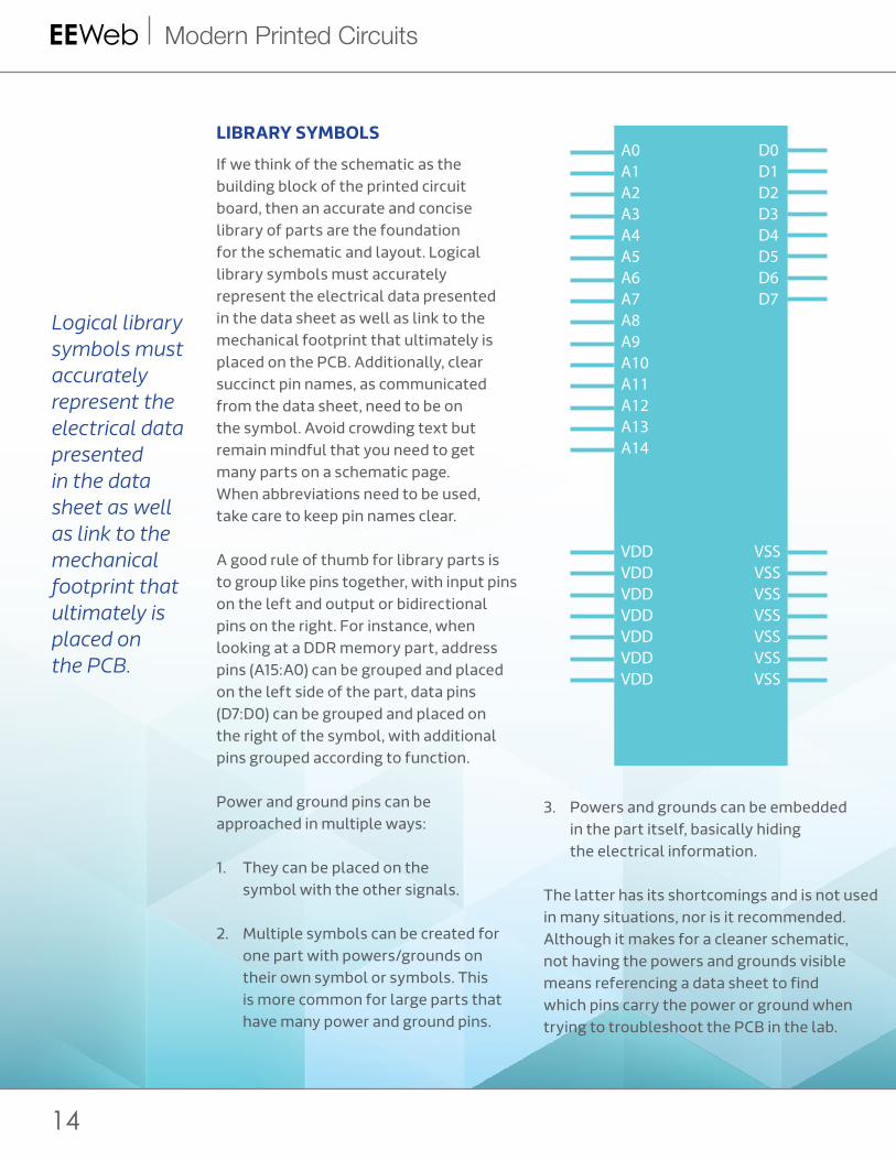
LIBRARY SYMBOLS
If we think of the schematic as the building block of the printed circuit board, then an accurate and concise library of parts are the foundation for the schematic and layout. Logical library symbols must accurately represent the electrical data presented in the data sheet as well as link to the mechanical footprint that ultimately is placed on the PCB. Additionally, clear succinct pin names, as communicated from the data sheet, need to be on the symbol. Avoid crowding text but remain mindful that you need to get many parts on a schematic page. When abbreviations need to be used, take care to keep pin names clear.
A good rule of thumb for library parts is to group like pins together, with input pins on the left and output or bidirectional pins on the right. For instance, when looking at a DDR memory part, address pins (A15:A0) can be grouped and placed on the left side of the part, data pins (D7:D0) can be grouped and placed on the right of the symbol, with additional pins grouped according to function.
Power and ground pins can be approached in multiple ways:
1. They can be placed on the symbol with the other signals.
2. Multiple symbols can be created for one part with powers/grounds on their own symbol or symbols. This is more common for large parts that have many power and ground pins.
3. Powers and grounds can be embedded in the part itself, basically hiding the electrical information.
The latter has its shortcomings and is not used in many situations, nor is it recommended. Although it makes for a cleaner schematic, not having the powers and grounds visible means referencing a data sheet to find which pins carry the power or ground when trying to troubleshoot the PCB in the lab.
During creation, keeping the size of pin symbols consistent will lead to a more aesthetically pleasing schematic. For example, two pin resistors, capacitors, and diodes should all take up roughly the same space on the schematic canvas. When building and using a schematic symbol, keep in mind that the symbol is meant to clearly show the electrical connectivity of the part and in no way is the symbol layout meant to reflect the actual mechanical layout of the footprint that will be placed on the printed circuit board.
SCHEMATIC BLOCKS
A very effective way to gather your thoughts and get the design committed to a certain form at the beginning is to start with a block diagram. Start with large generic blocks and then break each one into sub blocks. For instance, you may have a power supply block and a memory block.
The power supply block may have 5 volts, 3.3 volts, and 1.8 volts, with each of those blocks then containing the individual symbols necessary to generate those voltages. The memory block may contain a NAND and a DDR block. Each of those would contain the integrated circuit symbols, as well as any bypass capacitors and other associated circuitry. By breaking the design into these hierarchical blocks, which then may be associated to a single or multiple pages of the schematic, allows your design intention to be clearly added to paper.
SCHEMATIC
When placing symbols on the schematic, the information should be communicated as clearly as possible. Try to establish a left-to-right, top- to-bottom flow, similar to reading a book. Library symbols should have inputs on the left and outputs on the right, which lends itself to this methodology. Place symbols with plenty of room between them to allow connect lines to be drawn clearly and net information added without overlapping connect lines. Remember that, although you are viewing the schematic on a monitor in color, others may have only a black and white printout. Keep the reference designators near their respective symbols so there is no question about which component each belongs to.
A single symbol may map to several different footprints. When you make the selection to place it on the schematic, you are also selecting the footprint that will be on the PCB. For instance, the same resistor may be available in 0805, 0603, 0402, and 0201 footprint packages as well as radial or axial through hole.
Be consistent in your net naming throughout the schematic and embed as much information into the schematic description of the design as you can, as this will greatly enhance your layout. For instance, adding properties that define a clock signal as a differential pair communicates to the PCB designer information that is critical to the way the signals are routed and connected. Likewise, by defining addresses as a
Logical library symbols must accurately represent the electrical data presented in the data sheet as well as link to the mechanical footprint that ultimately is placed on the PCB.
When placing symbols on the schematic, the information should be communicated as clearly as possible.

15
EEWeb FEATURE
A0A1A2A3A4A5A6A7A8A9A10A11A12A13A14
D0D1D2D3D4D5D6D7
VSSVSSVSSVSSVSSVSSVSS
VDDVDDVDDVDDVDDVDDVDD
LIBRARY SYMBOLS
If we think of the schematic as the building block of the printed circuit board, then an accurate and concise library of parts are the foundation for the schematic and layout. Logical library symbols must accurately represent the electrical data presented in the data sheet as well as link to the mechanical footprint that ultimately is placed on the PCB. Additionally, clear succinct pin names, as communicated from the data sheet, need to be on the symbol. Avoid crowding text but remain mindful that you need to get many parts on a schematic page. When abbreviations need to be used, take care to keep pin names clear.
A good rule of thumb for library parts is to group like pins together, with input pins on the left and output or bidirectional pins on the right. For instance, when looking at a DDR memory part, address pins (A15:A0) can be grouped and placed on the left side of the part, data pins (D7:D0) can be grouped and placed on the right of the symbol, with additional pins grouped according to function.
Power and ground pins can be approached in multiple ways:
1. They can be placed on the symbol with the other signals.
2. Multiple symbols can be created for one part with powers/grounds on their own symbol or symbols. This is more common for large parts that have many power and ground pins.
3. Powers and grounds can be embedded in the part itself, basically hiding the electrical information.
The latter has its shortcomings and is not used in many situations, nor is it recommended. Although it makes for a cleaner schematic, not having the powers and grounds visible means referencing a data sheet to find which pins carry the power or ground when trying to troubleshoot the PCB in the lab.
During creation, keeping the size of pin symbols consistent will lead to a more aesthetically pleasing schematic. For example, two pin resistors, capacitors, and diodes should all take up roughly the same space on the schematic canvas. When building and using a schematic symbol, keep in mind that the symbol is meant to clearly show the electrical connectivity of the part and in no way is the symbol layout meant to reflect the actual mechanical layout of the footprint that will be placed on the printed circuit board.
SCHEMATIC BLOCKS
A very effective way to gather your thoughts and get the design committed to a certain form at the beginning is to start with a block diagram. Start with large generic blocks and then break each one into sub blocks. For instance, you may have a power supply block and a memory block.
The power supply block may have 5 volts, 3.3 volts, and 1.8 volts, with each of those blocks then containing the individual symbols necessary to generate those voltages. The memory block may contain a NAND and a DDR block. Each of those would contain the integrated circuit symbols, as well as any bypass capacitors and other associated circuitry. By breaking the design into these hierarchical blocks, which then may be associated to a single or multiple pages of the schematic, allows your design intention to be clearly added to paper.
SCHEMATIC
When placing symbols on the schematic, the information should be communicated as clearly as possible. Try to establish a left-to-right, top- to-bottom flow, similar to reading a book. Library symbols should have inputs on the left and outputs on the right, which lends itself to this methodology. Place symbols with plenty of room between them to allow connect lines to be drawn clearly and net information added without overlapping connect lines. Remember that, although you are viewing the schematic on a monitor in color, others may have only a black and white printout. Keep the reference designators near their respective symbols so there is no question about which component each belongs to.
A single symbol may map to several different footprints. When you make the selection to place it on the schematic, you are also selecting the footprint that will be on the PCB. For instance, the same resistor may be available in 0805, 0603, 0402, and 0201 footprint packages as well as radial or axial through hole.
Be consistent in your net naming throughout the schematic and embed as much information into the schematic description of the design as you can, as this will greatly enhance your layout. For instance, adding properties that define a clock signal as a differential pair communicates to the PCB designer information that is critical to the way the signals are routed and connected. Likewise, by defining addresses as a
Logical library symbols must accurately represent the electrical data presented in the data sheet as well as link to the mechanical footprint that ultimately is placed on the PCB.
When placing symbols on the schematic, the information should be communicated as clearly as possible.

www.aapcb.com
16
Modern Printed Circuits
Advanced Assembly was founded to help engineers assemble their prototype and low-volume PCB orders. Based on years of experience within the printed circuit board industry, Advanced Assembly developed a proprietary system to deliver consistent, machine surface mount technology (SMT) assembly in 1-5 days. It’s our only focus. We take the hassle out of PCB assembly and make it easy, so you can spend time on other aspects of your design.
20100 E. 32nd Pkwy #225 | Aurora, CO 80011 | www.aapcb.com | 1-800-838-5650
POWER MEMORY
5V 3.3V 1.8V NAND DDR
bus or setting minimum trace width properties in the schematic, you convey the information to the layout designer and ensure that requirements are not missed at the printed circuit board level. The goal is to put as much information as possible on the schematic to communicate the design intent while making it easy to read and understand.
The schematic is only as good as the library symbols and the data you include within it. Accurate information
at the start is a must. By creating a block diagram of the entire system and breaking those blocks into sub blocks, while remaining clear, concise, and consistent with your net naming conventions, will contribute to a highly functional PCB. Embed as much information as you can into the schematic to ensure it makes it to the layout. Ask colleagues to review your schematics and provide feedback. A good schematic does not happen overnight. It takes practice and will improve over time.
The schematic is only as good as the library symbols and the data you include within it.

CLICK HERESMT Assembly for Engineers
SMT Assembly for Engineers
SMT Assembly for Engineers

18
Modern Printed Circuits
When they look at an integrated circuit, most people do not realize that what they are looking at is simply the package that encapsulates the actual IC or
“the brains.” Integrated circuit packaging is something that happens to parts before they ever leave the manufacturing facility meaning that most designers and engineers never see the raw IC itself. Although the encapsulated IC may be the portion that brings value to the overall product, the package has an incredibly large effect on many different aspects of performance. While different packages are promoted by different manufacturers, along with their specific pros and cons, this article will discuss the packages in general and the different attributes to consider when making a selection.
PACKAGESNot Just for Christmas

19
EEWeb FEATURE
When they look at an integrated circuit, most people do not realize that what they are looking at is simply the package that encapsulates the actual IC or
“the brains.” Integrated circuit packaging is something that happens to parts before they ever leave the manufacturing facility meaning that most designers and engineers never see the raw IC itself. Although the encapsulated IC may be the portion that brings value to the overall product, the package has an incredibly large effect on many different aspects of performance. While different packages are promoted by different manufacturers, along with their specific pros and cons, this article will discuss the packages in general and the different attributes to consider when making a selection.
PACKAGESNot Just for Christmas

20
Modern Printed Circuits
The IC itself is typically a small piece of silicon that somehow needs to be protected from and interfaced to the outside world. The package not only protects the semiconductor from mechanical stresses but also from environmental stresses, keeping it out of the elements and away from potentially corrosive or damaging materials. Some packages also provide a certain amount of ESD protection, further shielding the IC from potential damage. While the package protects and fully encloses the IC, it also must be able to interface with other devices. While there are different ways of doing this, the most common is via wire bonding. With wire bonding, a machine stamps a small piece of wire onto a nearly microscopic pad on the semiconductor before connecting that wire to the leads of the package. There are a few different ways the machine stamps the pad on, but the process generally involves pressure, heat, and ultrasonic waves to securely attach the wire to the surfaces.
How the IC is placed inside the package is also highly variable, with the cheapest and most frequently being the molded plastic method.
Commonly, Dual-Inline Packages (DIPs) are enclosed in molded plastic. While low cost and mature as a technology, molded plastic has many trade-offs in terms of electrical conductivity and environmental protection.
Ironically, despite significant improvements over the years in the process of post-molded plastic packaging, the encapsulation process is also rather harsh. Other packaging types used are pressed ceramic and cofired laminate ceramic (both significantly more expensive than molded plastic), as well as chip on board (COB) technology. Done properly, pressed ceramic can create a hermetically sealed environment that will completely protect the IC from environmental factors. Cofired laminate ceramic is the most reliable packaging technology currently available on the market, making it ideal for avionics and military specs. COB actually dispenses with the packages completely and simply attaches the IC directly to a PCB. This PCB can be the final board that goes into the end product or it can have leads to connect it to either another PCB or another device.
As most consumer products use the plastic molded package material, the end designer’s bigger question is which package type to use. Dual inline, quad flat pack, ball grid array, thin shrink small outline - there are literally dozens of types of packages and hundreds of sub-categories within those types. The requirements for the project will narrow the choice down significantly, after considering the following characteristics:
• Heat dissipation – Larger packages are better at dissipating more heat and certain packages have specific pads or plates to help move heat away from the IC.
• High frequency – leadless packages are better for high frequency designs because the legs on other packages, particularly any through-hole package, increase the inductance on the line and will likely change the apparent impedance.
• Ease of soldering – while surface mount and leadless packages tend to be smaller, this in turn, makes them much more difficult to solder. Certain packages, such as the BGA, are nearly impossible to solder by hand, whereas a DIP package is trivial.
Dual Inline Package Ball Grid Array Quad Flat No-LeadsDual Inline Package Ball Grid Array Quad Flat No-LeadsDual Inline Package Ball Grid Array Quad Flat No-LeadsDual Inline Package Ball Grid Array Quad Flat No-Leads

21
EEWeb FEATURE
The IC itself is typically a small piece of silicon that somehow needs to be protected from and interfaced to the outside world. The package not only protects the semiconductor from mechanical stresses but also from environmental stresses, keeping it out of the elements and away from potentially corrosive or damaging materials. Some packages also provide a certain amount of ESD protection, further shielding the IC from potential damage. While the package protects and fully encloses the IC, it also must be able to interface with other devices. While there are different ways of doing this, the most common is via wire bonding. With wire bonding, a machine stamps a small piece of wire onto a nearly microscopic pad on the semiconductor before connecting that wire to the leads of the package. There are a few different ways the machine stamps the pad on, but the process generally involves pressure, heat, and ultrasonic waves to securely attach the wire to the surfaces.
How the IC is placed inside the package is also highly variable, with the cheapest and most frequently being the molded plastic method.
Commonly, Dual-Inline Packages (DIPs) are enclosed in molded plastic. While low cost and mature as a technology, molded plastic has many trade-offs in terms of electrical conductivity and environmental protection.
Ironically, despite significant improvements over the years in the process of post-molded plastic packaging, the encapsulation process is also rather harsh. Other packaging types used are pressed ceramic and cofired laminate ceramic (both significantly more expensive than molded plastic), as well as chip on board (COB) technology. Done properly, pressed ceramic can create a hermetically sealed environment that will completely protect the IC from environmental factors. Cofired laminate ceramic is the most reliable packaging technology currently available on the market, making it ideal for avionics and military specs. COB actually dispenses with the packages completely and simply attaches the IC directly to a PCB. This PCB can be the final board that goes into the end product or it can have leads to connect it to either another PCB or another device.
As most consumer products use the plastic molded package material, the end designer’s bigger question is which package type to use. Dual inline, quad flat pack, ball grid array, thin shrink small outline - there are literally dozens of types of packages and hundreds of sub-categories within those types. The requirements for the project will narrow the choice down significantly, after considering the following characteristics:
• Heat dissipation – Larger packages are better at dissipating more heat and certain packages have specific pads or plates to help move heat away from the IC.
• High frequency – leadless packages are better for high frequency designs because the legs on other packages, particularly any through-hole package, increase the inductance on the line and will likely change the apparent impedance.
• Ease of soldering – while surface mount and leadless packages tend to be smaller, this in turn, makes them much more difficult to solder. Certain packages, such as the BGA, are nearly impossible to solder by hand, whereas a DIP package is trivial.
Dual Inline Package Ball Grid Array Quad Flat No-LeadsDual Inline Package Ball Grid Array Quad Flat No-LeadsDual Inline Package Ball Grid Array Quad Flat No-LeadsDual Inline Package Ball Grid Array Quad Flat No-Leads

www.aapcb.com
22
Modern Printed Circuits
Advanced Assembly was founded to help engineers assemble their prototype and low-volume PCB orders. Based on years of experience within the printed circuit board industry, Advanced Assembly developed a proprietary system to deliver consistent, machine surface mount technology (SMT) assembly in 1-5 days. It’s our only focus. We take the hassle out of PCB assembly and make it easy, so you can spend time on other aspects of your design.
20100 E. 32nd Pkwy #225 | Aurora, CO 80011 | www.aapcb.com | 1-800-838-5650
• Cost – DIP packages are relatively inexpensive due to the mature technology behind them. However, the increased amount of material means that in larger quantities, price breaks are not as generous.
• Mechanical stability – some environments can see parts shaken and bumped directly, at times physically removing the parts from the board. Through hole parts are much better attached to the circuit board and can withstand greater abuse before failure.
• Size – smaller, portable devices require the absolute smallest packages feasible or the overall product becomes too large to be marketable.
• Pins – one of the reasons surface mount devices were developed is that the increasing number of pins on chips were making the chips unwieldy and grotesquely large. An
upper limit was being reached. Surface mount devices, particularly BGAs, are better at fitting a large amount of connections into an incredibly small space.
• Standardization – most chips are packaged in a standard package type, making it very easy for designers to immediately know what he or she is dealing with, then create footprints or swap out parts.
Packages for IC’s have been instrumental in creating devices that can withstand the rigors of daily use. In addition to this protection, the packaging can increase design flexibility in how they are integrated into the final product, as well as can change the electrical characteristics of the IC, whether for better or for worse. The correct or incorrect selection of the package types can mean success or failure of a project.

Schematics.com
Your Circuit Starts Here.Sign up to design, share, and collaborate
on your next project—big or small.
Click Here to Sign Up

24
Modern Printed Circuits
With Robert Froehlich and Xavier Pacheco of Bench 2 Bench
Bench 2 Bench Technologies
is a flexible circuit solutions provider based in
Fullerton, California. The company was founded on
the idea that ultra-high-density interconnects require
unique engineering considerations and technical
prowess to deliver differentiated products to the
customer. However, the flexible circuit technology
that Bench 2 Bench utilizes goes way beyond
flexibility—their flex boards can produce ultra-fine
features that add immense value to the customers.
The impressive ultra-fine specifications of their
technology are so unique, that many customers are
unable to find a comparable offshore option in both
quality and affordability, making Bench 2 Bench
a stable business model in a historically volatile
industry. EEWeb spoke with Robert Froelich and
Xavier Pacheco of Bench 2 Bench about the state of
the industry and how the company is able to produce
boards at impressively small sizes.
QA&

25
FLEX CIRCUIT FEATURE
With Robert Froehlich and Xavier Pacheco of Bench 2 Bench
Bench 2 Bench Technologies
is a flexible circuit solutions provider based in
Fullerton, California. The company was founded on
the idea that ultra-high-density interconnects require
unique engineering considerations and technical
prowess to deliver differentiated products to the
customer. However, the flexible circuit technology
that Bench 2 Bench utilizes goes way beyond
flexibility—their flex boards can produce ultra-fine
features that add immense value to the customers.
The impressive ultra-fine specifications of their
technology are so unique, that many customers are
unable to find a comparable offshore option in both
quality and affordability, making Bench 2 Bench
a stable business model in a historically volatile
industry. EEWeb spoke with Robert Froelich and
Xavier Pacheco of Bench 2 Bench about the state of
the industry and how the company is able to produce
boards at impressively small sizes.
QA&

26
Modern Printed Circuits
In your words, what is Bench 2 Bench all about?
Bench 2 Bench Technologies has been in existence for a little over six years. We are a part of a family of three circuit board facilities that are a part of a larger company called JR Controls. The three
circuit board facilities are Bench 2 Bench, which is a flex circuit manufacturer, Winonics, which is a commercial rigid-board manufacturer, and Cosmotronic, which does rigid-flex boards aimed at the military industry. Our facility had been a rigid-board facility for a number of years and the owner, Rod Savage, was determined to convert it to
a flex-circuit operation. Our current team was brought on board to convert it from a commercial rigid-board facility to a flexible circuit manufacturing facility. The people he brought on board had a lot of experience in flexible circuits for the medical marketplace, and our focus has been on capturing business in the medical sphere.
What was the main factor that drove the conversion from rigid-board to flex-circuit?
If you are involved in the circuit board industry in the U.S., you realize that, when it comes to rigid boards, the market is very difficult. The business is going offshore and it is difficult to stop that transition, so you need to look at how to diversify your business portfolio. Rod Savage thought it was a great idea
to look at new opportunities and be more diversified, which was the right thing to do. By having a flex-circuit, rigid-board, and military facilities, we have been able to accomplish this.
Could you describe how the properties of flex-boards differ from rigid-boards?
Flex-boards are created with a very thin substrate material as opposed to a rigid, thick board. This allows for the folding manipulation of the end product. Because of the density, it allows for thinner, lighter packages for the applications. A typical rigid-board might be 62 thousandths of an inch, and our flex-circuit product could be 3-mils thick—or 1/20th of the thickness of a standard rigid-board. Flexible circuits must be able to wrap, bend, and conform to different shapes in the end application, whereas a rigid board is flat. A rigid-flex board has areas that can be bent, but it is a much thicker and not as pliable.
Why is it that flex-boards are harder to outsource?
A lot of flexible circuits are done in Asia, which go into a lot of popular mobile devices. Flex-circuits can be used in everything from ink cartridges to cellphones, and as you can imagine, those volumes are extremely high. When you have low-mix, high-volume requirements, that is usually the reason why many choose to go offshore. When you have high mix, a lot of different part numbers, and the volumes are lower, those are the types of products that stay
in the U.S. That is why our focus is on the medical marketplace, because we make a lot of different part numbers and the quantities we make are relatively small.
The name of our company Bench 2 Bench Technologies means “from our engineering bench to your engineering bench.” This is a symbol of the kind of communication we want to have with our customers. When our customer has a design, they communicate with us and we are able to work with them to interpret the design and do what we do best. Part of the reason why we have been successful is because of these relationships we have with our customers.
What are some of the technical parameters of your flex-boards in terms of line-width, spacing, and pitch and how do these compare to your competitor’s?
We are able to go down to a 50-micron pitch, which represents a 25-micron line or 1-mil line. Of course, that is material dependent, which is another area that we have a wide array of materials available, ranging from 2-micron copper on up. We also have polyimide substrates as thin as 12-microns—with 2-micron copper produces a very thin flex circuit with very fine-line capability.
UHDI Flex with 50 micron vias
Multilayer flex with 50 micron vias/ 50 micron traces
Sub 25 micron traces
Flexible circuits must be able to wrap, bend, and conform to different shapes in the end application,
whereas a rigid board is flat.
When you do a 25-micron trace with a 25-micron space, you are really pushing the envelope. People are starting to go lower, and we are looking at finding the technology to do even higher density than what we are currently doing. That is definitely what we are focusing on for the future.
How much current can these boards handle?
We are targeting the medical market—in particular the ultrasound imaging space—which means there is very low current applied to these products. That is really a more signal-carrying path for them—it is an interface between the actual acoustic stack, which transforms an electrical signal into a mechanical signal, or sound wave. It typically sends and receives like a Sonar device and processes signals, which does not take a lot of power to happen.
What were some of the most challenging designs you have had to build?
The types of devices with really fine pitches and super-thin substrates are particularly challenging. When you are dealing with sizes down to the 12-micron range, or half-mil thick, it is almost like handling tissue paper with copper on
The types of devices with
really fine pitches and super-thin
substrates are particularly challenging.

27
FLEX CIRCUIT FEATURE
In your words, what is Bench 2 Bench all about?
Bench 2 Bench Technologies has been in existence for a little over six years. We are a part of a family of three circuit board facilities that are a part of a larger company called JR Controls. The three
circuit board facilities are Bench 2 Bench, which is a flex circuit manufacturer, Winonics, which is a commercial rigid-board manufacturer, and Cosmotronic, which does rigid-flex boards aimed at the military industry. Our facility had been a rigid-board facility for a number of years and the owner, Rod Savage, was determined to convert it to
a flex-circuit operation. Our current team was brought on board to convert it from a commercial rigid-board facility to a flexible circuit manufacturing facility. The people he brought on board had a lot of experience in flexible circuits for the medical marketplace, and our focus has been on capturing business in the medical sphere.
What was the main factor that drove the conversion from rigid-board to flex-circuit?
If you are involved in the circuit board industry in the U.S., you realize that, when it comes to rigid boards, the market is very difficult. The business is going offshore and it is difficult to stop that transition, so you need to look at how to diversify your business portfolio. Rod Savage thought it was a great idea
to look at new opportunities and be more diversified, which was the right thing to do. By having a flex-circuit, rigid-board, and military facilities, we have been able to accomplish this.
Could you describe how the properties of flex-boards differ from rigid-boards?
Flex-boards are created with a very thin substrate material as opposed to a rigid, thick board. This allows for the folding manipulation of the end product. Because of the density, it allows for thinner, lighter packages for the applications. A typical rigid-board might be 62 thousandths of an inch, and our flex-circuit product could be 3-mils thick—or 1/20th of the thickness of a standard rigid-board. Flexible circuits must be able to wrap, bend, and conform to different shapes in the end application, whereas a rigid board is flat. A rigid-flex board has areas that can be bent, but it is a much thicker and not as pliable.
Why is it that flex-boards are harder to outsource?
A lot of flexible circuits are done in Asia, which go into a lot of popular mobile devices. Flex-circuits can be used in everything from ink cartridges to cellphones, and as you can imagine, those volumes are extremely high. When you have low-mix, high-volume requirements, that is usually the reason why many choose to go offshore. When you have high mix, a lot of different part numbers, and the volumes are lower, those are the types of products that stay
in the U.S. That is why our focus is on the medical marketplace, because we make a lot of different part numbers and the quantities we make are relatively small.
The name of our company Bench 2 Bench Technologies means “from our engineering bench to your engineering bench.” This is a symbol of the kind of communication we want to have with our customers. When our customer has a design, they communicate with us and we are able to work with them to interpret the design and do what we do best. Part of the reason why we have been successful is because of these relationships we have with our customers.
What are some of the technical parameters of your flex-boards in terms of line-width, spacing, and pitch and how do these compare to your competitor’s?
We are able to go down to a 50-micron pitch, which represents a 25-micron line or 1-mil line. Of course, that is material dependent, which is another area that we have a wide array of materials available, ranging from 2-micron copper on up. We also have polyimide substrates as thin as 12-microns—with 2-micron copper produces a very thin flex circuit with very fine-line capability.
UHDI Flex with 50 micron vias
Multilayer flex with 50 micron vias/ 50 micron traces
Sub 25 micron traces
Flexible circuits must be able to wrap, bend, and conform to different shapes in the end application,
whereas a rigid board is flat.
When you do a 25-micron trace with a 25-micron space, you are really pushing the envelope. People are starting to go lower, and we are looking at finding the technology to do even higher density than what we are currently doing. That is definitely what we are focusing on for the future.
How much current can these boards handle?
We are targeting the medical market—in particular the ultrasound imaging space—which means there is very low current applied to these products. That is really a more signal-carrying path for them—it is an interface between the actual acoustic stack, which transforms an electrical signal into a mechanical signal, or sound wave. It typically sends and receives like a Sonar device and processes signals, which does not take a lot of power to happen.
What were some of the most challenging designs you have had to build?
The types of devices with really fine pitches and super-thin substrates are particularly challenging. When you are dealing with sizes down to the 12-micron range, or half-mil thick, it is almost like handling tissue paper with copper on
The types of devices with
really fine pitches and super-thin
substrates are particularly challenging.

28
Modern Printed Circuits
it that you have to produce conductive elements with. Handling becomes very difficult with thin substrates like that. A speck of dust would literally wipe out a conductor that thin, so cleanliness is just as crucial to consider.
How many layers are you able to achieve, and can you incorporate vias when you are working with such thin materials?
We can do up to six layers. Via-to-layer registration is important because when you are driving a 25-micron via through those layers, making an electrical connection is still the end goal. Everything we do is basically laser driven. We have laser-writing devices for photo resist and photo imaging, and we also do laser drilling. Mechanical drilling is for products that have larger holes and thicknesses. With lasers, we are able to place a 25-micron via on a 75-micron pad. For the flex-circuit industry, this is pretty unique.
What do you down the road for Bench 2 Bench in the next five years?
We know where we need to be in terms of technology. We are facing demands for finer lines and tighter-pitch products, but the investment aspect is where our customers also want us to go. We want to stage ourselves to be in a position
to be able to respond to those types of demands and requirements that our customers come to us with. We need to be able to do what we are doing today, but better. If we can do this more efficiently with better yields, then we can maintain a sustainable business.
You mentioned moving to even smaller sizes—do you see an end-point to where you are unable to get any smaller? Do you have any ideas as to what could lead to better performance?
More layers are always an option, but you are restricted as far as material. The suppliers of some of these materials also face limitations in producing thinner and better substrates. There are defects inherent in the substrate that create issues for us, so we need to work with them as well. We hope to innovate for things like sputtering-deposition as opposed to electro-plating copper. Those are the types of things that are dependent on our abilities as well as the material supplier’s abilities. Right now, our sweet spot is subtractive processes, meaning we would form circuits by etching copper and photo-printing it. The future is clearly in going to an additive process where you start off with polyimide substrate materials and adding traces to that. This is the most effective way to achieve even finer traces.
We are targeting the medical market—in particular the ultrasound imaging space—which means there is very low
current applied to these products.
Everything we do is basically laser driven.
We have laser-writing devices for photo resist
and photo imaging, and
we also do laser drilling.

http://www.epectec.com/
30
Modern Printed Circuits
Epec’s Flex and Rigid-flex Boards
If there are any true constants in the formula for the evolution of
modern electronics, the push to work at increasingly smaller scales
arguably tops the list. Where convenience and practicality collide,
size always stands as a common factor. So while today’s electronic
devices find themselves subject to a kind of expectation of constant
evolution of scale, the people behind the scenes, like the team
at Epec Engineered Technology, are naturally working faster and
harder than ever to do the work that makes it possible.
FITWhere No Other Designs Can

31
FLEX CIRCUIT FEATURE
Epec’s Flex and Rigid-flex Boards
If there are any true constants in the formula for the evolution of
modern electronics, the push to work at increasingly smaller scales
arguably tops the list. Where convenience and practicality collide,
size always stands as a common factor. So while today’s electronic
devices find themselves subject to a kind of expectation of constant
evolution of scale, the people behind the scenes, like the team
at Epec Engineered Technology, are naturally working faster and
harder than ever to do the work that makes it possible.
FITWhere No Other Designs Can

www.epectec.com/flex/
http://www.epectec.com/flex/material-stackup.html
32
Modern Printed Circuits
Of course, the work of keeping up with the march of downscaling requires a lot more than simply implementing yesterday’s technologies in smaller applications. As the needs and expectations of designers has passed the point of standard component capabilities, highly innovative technologies like flex and rigid-flex circuit board technology have emerged and developed to offer new angles of approach to improving the range of scale. Working specifically to optimize and streamline the application of this impressive emerging technology while still pushing the capability envelope, Epec Technology is helping to make flex and rigid-flex PCB’s a feasible technology for more applications all the time.
Paul Tome, Epec’s Flex and Rigid-Flex Product Manager and a twenty-six-year veteran of flex technology development, says that Epec prefers to work from the ground up with customers to give them the best possible experience in implementing it into their designs. “Initially, we put ourselves to the task of learning every step of how to create a flexible circuit,” he recalls, “in order to be sure that we could handle every part of the process correctly and to test everything as expertly as possible.”
Just like their names imply, flex and rigid-flex circuit boards integrate flexible materials into circuit board design to allow circuits and components to fit into more spaces than traditional rigid boards. On one hand, Tome informs us, so-called ‘flex’ materials are often used in combination with rigid boards in a sort
of either/or combination that allows for connection-and-component-heavy sections of rigid board to be attached by flexible sections. This allows for a first-level improvement in the ability to address space and density in a design, but, as Tome specifies, the use of truly composite ‘rigid-flex’ materials is what really allows for the greatest range of application. In rigid-flex technology, the flexible materials are integrated uniformly into the substrate of the circuit, offering flexibility equally at every point while still allowing for reliable connections.
While flex technology can be considered a concept that applies to scenarios as simple as using copper that is thin enough to offer some marginal flexibility, it’s something that has come a long way very quickly in recent years. “Flex and rigid-flex is now at a level that allows customers to customize packaging to a degree that is unmatched by any other available interconnect method in the electronics industry,” Tome asserts. “In many cases,” he says in regard to today’s common packaging requirements, “flex and rigid-flex are the only real options.“. “ As the companys find themselves working more and more in an essential role to facilitate the constant evolution of downscaling, and as designers in general move increasingly beyond the frontiers of the capabilities of rigid circuit boards, Epec’s work with flex and rigid-flex seems to suggest exciting things for new standards in the industry.
As if the technology’s abilities to address space and density issues weren’t enough, Tome informs us that flex and rigid-flex can also serve to improve the overall reliability of designs. “In higher-end medical applications, or military applications, cases which can be thought of as more ‘life and death’ situations,” he points out, “designers will often turn to a flex or rigid-flex solution simply for the sake of achieving the highest degree of reliability in their design.” Essentially, he explains, flex and rigid-flex can greatly reduce the amount of interconnect points within a design, and in these cases in particular, each point of interconnect is also considered a point of potential failure.
Some of the The materials being used for flex and rigid-flex today are remarkably thin, with some of Epec’s polyimide products coming in as thin as 0.1mm. In the form of what is known as Polyimide or Kapton, a plastic polymer comparable to Mylar, Epec’s boards provide exceptional electrical performance and a significant respectable resistance to most common chemical wear. With a wide range of products available, Epec provides both circuits that are designed specifically to offer lower production costs, and those that are focused on providing additional, specialized functionality, with support at every stage.
Beyond the general demands of working with such sensitive materials, Tome notes that the biggest challenge in today’s market is meeting both the electrical and the mechanical requirements of increasingly dense designs. “A lot of times, these two requirements are at odds with one another,” he reflects, “and where bend requirements call for a certain thickness, electrical requirements are calling for something else for the sake of current or signal integrity.” It’s certainly no surprise that the productive conflict between demand and capability is keeping Epec on their toes.
“The biggest challenge in manufacturing flex and rigid-flex circuits is actually an issue inherent to the materials themselves,” Tome admits. Ultimately, he says, it’s the lack of dimensional stability in the materials, especially when working with very large or very small designs. “These materials will grow, shrink, and generally distort in a variety of ways as they go through the various steps of the manufacturing process,” he describes. As might also be expected, the benefits provided by flex technology also double as potential difficulties in the production stage. “There are very specific material handling challenges,” Tome describes. These, naturally, are very easily damaged, so handling requires some specific attention.
Flex and rigid-flex
circuit boards integrate flexible
materials into circuit
board design to allow
circuits and components
to fit into more
spaces than traditional
rigid boards.
“These materials will grow, shrink, and generally distort in a variety of ways as they go through the
various steps of the manufacturing process.”

http://www.epectec.com/flex/material-properties.html
33
FLEX CIRCUIT FEATURE
Of course, the work of keeping up with the march of downscaling requires a lot more than simply implementing yesterday’s technologies in smaller applications. As the needs and expectations of designers has passed the point of standard component capabilities, highly innovative technologies like flex and rigid-flex circuit board technology have emerged and developed to offer new angles of approach to improving the range of scale. Working specifically to optimize and streamline the application of this impressive emerging technology while still pushing the capability envelope, Epec Technology is helping to make flex and rigid-flex PCB’s a feasible technology for more applications all the time.
Paul Tome, Epec’s Flex and Rigid-Flex Product Manager and a twenty-six-year veteran of flex technology development, says that Epec prefers to work from the ground up with customers to give them the best possible experience in implementing it into their designs. “Initially, we put ourselves to the task of learning every step of how to create a flexible circuit,” he recalls, “in order to be sure that we could handle every part of the process correctly and to test everything as expertly as possible.”
Just like their names imply, flex and rigid-flex circuit boards integrate flexible materials into circuit board design to allow circuits and components to fit into more spaces than traditional rigid boards. On one hand, Tome informs us, so-called ‘flex’ materials are often used in combination with rigid boards in a sort
of either/or combination that allows for connection-and-component-heavy sections of rigid board to be attached by flexible sections. This allows for a first-level improvement in the ability to address space and density in a design, but, as Tome specifies, the use of truly composite ‘rigid-flex’ materials is what really allows for the greatest range of application. In rigid-flex technology, the flexible materials are integrated uniformly into the substrate of the circuit, offering flexibility equally at every point while still allowing for reliable connections.
While flex technology can be considered a concept that applies to scenarios as simple as using copper that is thin enough to offer some marginal flexibility, it’s something that has come a long way very quickly in recent years. “Flex and rigid-flex is now at a level that allows customers to customize packaging to a degree that is unmatched by any other available interconnect method in the electronics industry,” Tome asserts. “In many cases,” he says in regard to today’s common packaging requirements, “flex and rigid-flex are the only real options.“. “ As the companys find themselves working more and more in an essential role to facilitate the constant evolution of downscaling, and as designers in general move increasingly beyond the frontiers of the capabilities of rigid circuit boards, Epec’s work with flex and rigid-flex seems to suggest exciting things for new standards in the industry.
As if the technology’s abilities to address space and density issues weren’t enough, Tome informs us that flex and rigid-flex can also serve to improve the overall reliability of designs. “In higher-end medical applications, or military applications, cases which can be thought of as more ‘life and death’ situations,” he points out, “designers will often turn to a flex or rigid-flex solution simply for the sake of achieving the highest degree of reliability in their design.” Essentially, he explains, flex and rigid-flex can greatly reduce the amount of interconnect points within a design, and in these cases in particular, each point of interconnect is also considered a point of potential failure.
Some of the The materials being used for flex and rigid-flex today are remarkably thin, with some of Epec’s polyimide products coming in as thin as 0.1mm. In the form of what is known as Polyimide or Kapton, a plastic polymer comparable to Mylar, Epec’s boards provide exceptional electrical performance and a significant respectable resistance to most common chemical wear. With a wide range of products available, Epec provides both circuits that are designed specifically to offer lower production costs, and those that are focused on providing additional, specialized functionality, with support at every stage.
Beyond the general demands of working with such sensitive materials, Tome notes that the biggest challenge in today’s market is meeting both the electrical and the mechanical requirements of increasingly dense designs. “A lot of times, these two requirements are at odds with one another,” he reflects, “and where bend requirements call for a certain thickness, electrical requirements are calling for something else for the sake of current or signal integrity.” It’s certainly no surprise that the productive conflict between demand and capability is keeping Epec on their toes.
“The biggest challenge in manufacturing flex and rigid-flex circuits is actually an issue inherent to the materials themselves,” Tome admits. Ultimately, he says, it’s the lack of dimensional stability in the materials, especially when working with very large or very small designs. “These materials will grow, shrink, and generally distort in a variety of ways as they go through the various steps of the manufacturing process,” he describes. As might also be expected, the benefits provided by flex technology also double as potential difficulties in the production stage. “There are very specific material handling challenges,” Tome describes. These, naturally, are very easily damaged, so handling requires some specific attention.
Flex and rigid-flex
circuit boards integrate flexible
materials into circuit
board design to allow
circuits and components
to fit into more
spaces than traditional
rigid boards.
“These materials will grow, shrink, and generally distort in a variety of ways as they go through the
various steps of the manufacturing process.”
34
Modern Printed Circuits
Addressing the company’s particular specialty in the flex and rigid-flex markets, Tome concludes that Epec succeeds by providing a uniquely complete approach to implementing the technology, by presenting the widest possible range of permutational options, offering guidance with an independent expertise on every level of design, and by providing customers with multiple manufacturing facilities to allow for a completely customized process from start to finish. “In most cases, our design support will come into play right off the bat, in the earliest conceptual planning stages,” he asserts.
As customers weigh alternatives for solving their design requirements, Tome recognizes, companies hoping to keep up have to be able to qualify their
technology for a variety of solutions. “In the five years that I’ve been with Epec, we’ve achieved a remarkable amount of growth with the product line,” he observes. And, as he puts it succinctly, it doesn’t hurt that Epec’s top-to-bottom system “allows us to do the best possible job of keeping the bigger picture of cost in mind through the whole journey.” With the best possible service at every level of the application of flex and rigid-flex technology square in their sights, and a professed keen eye toward burgeoning technologies like the new wave of wearables, Tome and the team at Epec seem to have every reason to look forward to a widening frontier to help balance out the growing pains of the non-stop race to downsize.
With a wide range of products available, Epec provides both circuits that are designed
specifically to offer lower production costs, and those that are focused on providing additional, specialized
functionality, with support at every stage.

Click here
Sierra Circuits:A Complete PCB Resource
PLUS: The Ground ” Myth in PrintedCircuits
“
PCB Resin Reactor+
Ken BahlCEO of Sierra Circuits
Let There Be
How Cree reinvented the light bulb
LIGHT
David ElienVP of Marketing & Business
Development, Cree, Inc.
New LED Filament Tower
Cutting Edge Flatscreen Technologies
+
+
M o v i n g T o w a r d s
a Clean Energy
FUTURE— Hugo van Nispen, COO of DNV KEMA
MCU Wars 32-bit MCU Comparison
Cutting Edge
SPICEModeling
Freescale and TI Embedded
Modules
ARMCortex
Programming
From Concept to
Reality Wolfgang Heinz-Fischer
Head of Marketing & PR, TQ-Group
Low-Power Design Techniques
TQ-Group’s Comprehensive Design Process
+
+
PowerDeveloper
Octobe r 20 13
Designing forDurability
View more EEWeb magazines— Click Here