Embed Size (px)
Citation preview

Modelling the thermoresistive properties of silicon and germanium in a wide regionof temperature variation
V. K. Grunin
St. Petersburg State Electrical Engineering University, St. Petersburg, Russia~Submitted January 18, 1999!Opticheski� Zhurnal66, 103–105~August 1999!
Mathematical modelling is used to study the temperature dependences of the resistivities ofextrinsic germanium and silicon in the interval from about 1 K to 800 K, including the regimes ofhopping, extrinsic~in the states of freezing out and depletion of the impurity!, and intrinsicelectrical conductivity. The temperature coefficients of Ge and Si vary from260 to 0.015 K21.© 1999 The Optical Society of America.@S1070-9762~99!01808-4#
orte
wialo
linor
emen
ria
iea
n-
Gs
outubeduan
n
onngen
lar
ehr
xityfullo
cal-
fora-eri-
them-ere,
by
-theon-
rveo-
on-en-ndata0–
nded
ons-
e-
ar-
han
ndor-
Extrinsic silicon and germanium are the semiconductthat are most often used to create bolometric radiation detors capable of operating both at room temperature anddeep cooling.1,2 In this connection, it seems expedient to cculate their thermoresistive properties in a wide intervaltemperature variation, using modern mathematical modelmethods for this to provide symbolic mathematical transfmations~Mathcad 6.0 Plus or Mathcad 7.0 Prof.!.
This paper discusses the results of a study of the tperature dependence of the resistivity of weakly compsatedp-Ge:Ga withNa51022m23 and n-Si:Sb havingNd
51022m23. The degree of compensation of each mateequalled 0.1. The temperature boundaries that separatedifferent electrical-conductivity regimes and the free-carrconcentrations in the bands were calculated taking intocount the degeneracy multiplicity of the impurity states (ga
51/4 in p-Ge, gd52 in n-Si! and the temperature depedence of the band gap.3 The intrinsic electrical conductivityregime was established at a temperature above 470 K inand 680 K in Si. Extrinsic electrical conductivity in Ge waobserved in the temperature interval from 470 K to ab10 K, the impurity-depletion state appeared at a temperaabove about 30 K; hopping electrical conductivity was oserved below 10 K. Extrinsic conductivity in Si correspondto the temperature interval from 680 K to about 20 K, imprity depletion appeared at a temperature above 65 K,hopping conductivity was observed below 20 K.
The temperature dependences of the resistivityrs(T) ofsilicon andrg(T) of germanium are shown in Fig. 1. Oeach curve, the linear sections of increasing resistance onlow-temperature side correspond to hopping electrical cductivity. Beyond the conventional boundary of hoppiconductivity, a temperature at which the free-carrier conctration in the allowed bands did not exceed 1025 of the con-centration of the main impurity was assumed in the calcution. The sharp falloff of the resistance from this boundaon the high-temperature side is caused by the increasthermal generation in the regime of carrier freeze-out. Tminimum resistance is observed at the boundary of thegions of freeze-out and of impurity depletion and appromately coincides with the maximum mobility of the majoricarriers in each material. As the temperature increasesther, the impurity-depletion state ceases, and a sharp faappears in the resistance in the intrinsic conductivity regim
755 J. Opt. Technol. 66 (8), August 1999 1070-9762/99/0807
sc-th-fg-
--
ltherc-
e
tre-
-d
the-
-
-yofee--
r-ff
e.
The temperature dependences of the resistivity wereculated for various constant activation energiesEj of thehopping conductivity; the curves in Fig. 1 are obtainedactivation energies of 5 meV in silicon and 3 meV in germnium. The activation energies were chosen from the expmental data for weakly compensated silicon4 andgermanium5 closest to the values assumed in calculatingconcentration of the main impurity and the degree of copensation of the semiconductor. In the model discussed hthe variation of the carrier mobility inn-Si with temperaturewas approximated in the temperature region above 30 Kthe power lawsT22.4 for electrons andT22.2 for holes, withthe carriers being scattered at phonons,3 whereas, at temperatures below 30 K, with scattering at charged impurities,electron mobility was taken to be proportional to the fractiT1.5/2Na , whereNa51021m23 is the concentration of compensating acceptor impurity inn-Si. Similarly, in p-Ge, thelaws T22.33 for holes andT21.66 for electrons were used fothe variation of the carrier mobility at temperatures abo25 K,3 whereas, for temperatures below 25 K, the hole mbility was assumed to be proportional to the fractiT1.5/2Nd , whereNd51021m23 is the concentration of compensating donor impurity. The calculated temperature depdences of the resistivity of silicon and germanium are fouto be in satisfactory agreement with the experimental davailable in the literature in the temperature interval 1300 K for silicon4 and in the interval 3–100 K forgermanium.5
The temperature coefficients of resistivity of silicon agermanium in a wide temperature interval were determinfrom a(T)5@1/r(T)#dr(T)/dT after symbolic differentia-tion with respect to temperature of the analytical expressifor the resistivity of the material in various conductivity regimes.
The variations of the temperature coefficientsa js(T) ofsilicon anda jg(T) of germanium in the region ofhoppingconductivityare shown in Fig. 2. Analysis shows that a dpendence of the forma j (T);2Ej /T2 is followed in thisregion the more closely the lower is the temperature; in pticular, the ratio a jg(T)/a js(T)>Ejg /Ejs when T,1 K,whereas the ratio of the coefficients increases by more t10% by comparison withEjg /Ejs whenT.1 K. A compari-son of the calculated temperature coefficients of silicon agermanium in the temperature interval 4–13 K with the c
75555-03$15.00 © 1999 The Optical Society of America
eIte
ucuc
-
An
li-
ts ia
nfeth
inon-andee-
kly
pec-nce
ra-Si
at,
turese
on
responding values obtained by approximating the experimtal data2,4,5 displays a divergence by a factor of 1.5–2.follows from this that it is important to exactly determine thenergyEj , the degree of compensation of the semicondtor, and the boundaries of the region of hopping condtivity.
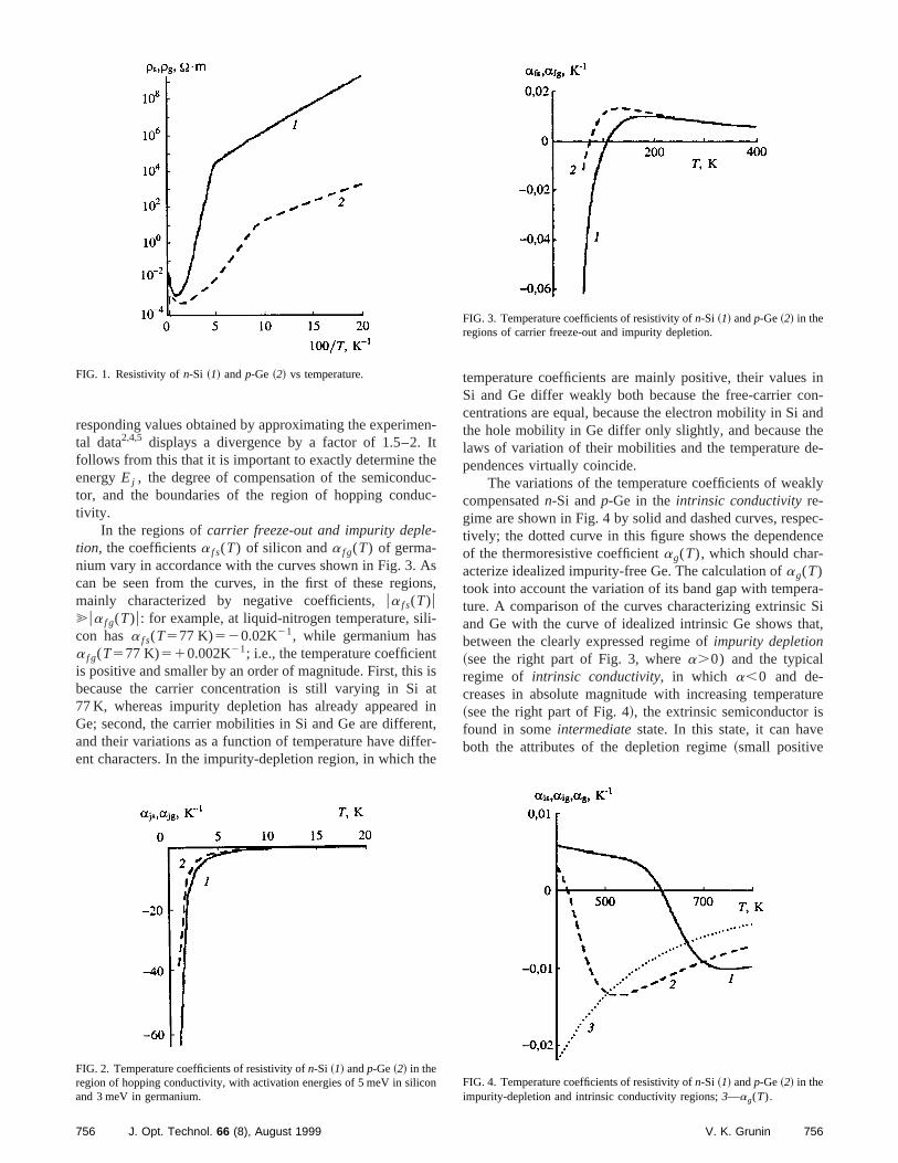
In the regions ofcarrier freeze-out and impurity depletion, the coefficientsa f s(T) of silicon anda f g(T) of germa-nium vary in accordance with the curves shown in Fig. 3.can be seen from the curves, in the first of these regiomainly characterized by negative coefficients,ua f s(T)u@ua f g(T)u: for example, at liquid-nitrogen temperature, sicon hasa f s(T577 K)520.02K21, while germanium hasa f g(T577 K)510.002K21; i.e., the temperature coefficienis positive and smaller by an order of magnitude. First, thibecause the carrier concentration is still varying in Si77 K, whereas impurity depletion has already appearedGe; second, the carrier mobilities in Si and Ge are differeand their variations as a function of temperature have difent characters. In the impurity-depletion region, in which
FIG. 1. Resistivity ofn-Si ~1! andp-Ge ~2! vs temperature.
FIG. 2. Temperature coefficients of resistivity ofn-Si ~1! andp-Ge~2! in theregion of hopping conductivity, with activation energies of 5 meV in silicand 3 meV in germanium.
756 J. Opt. Technol. 66 (8), August 1999
n-
--
ss,
stint,r-e
temperature coefficients are mainly positive, their valuesSi and Ge differ weakly both because the free-carrier ccentrations are equal, because the electron mobility in Sithe hole mobility in Ge differ only slightly, and because thlaws of variation of their mobilities and the temperature dpendences virtually coincide.
The variations of the temperature coefficients of weacompensatedn-Si andp-Ge in theintrinsic conductivityre-gime are shown in Fig. 4 by solid and dashed curves, restively; the dotted curve in this figure shows the dependeof the thermoresistive coefficientag(T), which should char-acterize idealized impurity-free Ge. The calculation ofag(T)took into account the variation of its band gap with tempeture. A comparison of the curves characterizing extrinsicand Ge with the curve of idealized intrinsic Ge shows thbetween the clearly expressed regime ofimpurity depletion~see the right part of Fig. 3, wherea.0) and the typicalregime of intrinsic conductivity, in which a,0 and de-creases in absolute magnitude with increasing tempera~see the right part of Fig. 4!, the extrinsic semiconductor ifound in someintermediatestate. In this state, it can havboth the attributes of the depletion regime~small positive
FIG. 3. Temperature coefficients of resistivity ofn-Si ~1! andp-Ge~2! in theregions of carrier freeze-out and impurity depletion.
FIG. 4. Temperature coefficients of resistivity ofn-Si ~1! andp-Ge~2! in theimpurity-depletion and intrinsic conductivity regions;3—ag(T).
756V. K. Grunin

al-uc.Gft
u
des othme
re-ing
of3.
i-
’’
.
a-
values ofa, decreasing as temperature increases!, and theattributes of the intrinsic conductivity regime—negative vues ofa, whose absolute value, despite the intrinsic condtivity properties, increases with increasing temperaturecan be seen from Fig. 4 that, in the extrinsic Si andconsidered here, such states are observed to the left ocalculated values of the temperature of their transitionintrinsic conductivity~470 K in Ge and 680 K in Si!. Thesetemperature intervals can have practical significancechoosing the working temperatures of uncooled semicondtor bolometers.
In conclusion, we should point out that the method unconsideration of calculating the thermoresistive propertieextrinsic semiconductors can be improved by improvingaccuracy of the temperature dependences of the carrierbility and by explaining how the doping levels and the d
757 J. Opt. Technol. 66 (8), August 1999
-Itetheo
inc-
rf
eo-
-
gree of compensation of the semiconductor affect the pexponential factor and the activation energy of the hoppconductivity.
This work was carried out with the support of a grantthe Federal Special Program ‘‘Integration,’’ Project No. 20
1B. S. Smolyanski�, Yu. I. Moiseev, S. B. Stanevich, ‘‘The BSG-2 semconductor bolometer,’’ inThermal Radiation Detectors~Gos. Opt. Inst.,Leningrad, 1971!, pp. 12–15.
2Yu. V. Kulikov, ‘‘Semiconductor materials of cryogenic bolometers,in Thermal Radiation Detectors~Gos. Opt. Inst., Leningrad, 1990!,pp. 10–13.
3S. M. Sze,Physics of Semiconductor Devices~Wiley, New York, 1969;Mir, Moscow, 1984, 456 pp.!.
4R. K. Ray and H. Y. Fan, ‘‘Impurity conduction in silicon,’’ Phys. Rev121, 768 ~1961!.
5C. S. Hung and J. R. Gliessman, ‘‘Resistivity and Hall Effect of Germnium at Low Temperatures,’’ Phys. Rev.96, 1226~1954!.
757V. K. Grunin