Embed Size (px)
Citation preview

Germanium Detectors
Greg Hackman

Generic Electronic Radia6on Detector • Radia6on (slanted arrow) passes
through ma<er • (this is a charged par6cle)
• Collisions create charged-‐par6cle pairs (e.g. free electrons, ions)
• Electric field sweeps up free charge to contacts
• Transient electric current pulse amplified & processed
• What is the grey stuff? • Gas • Semiconductor diode

What’s special about HPGe? • High Purity Germanium (HPGe) • Good tradeoff between energy resolu6on and efficiency
Applica6ons of Ge
• Nuclear Physics and Chemistry – Excited levels within
nuclear system -‐-‐ i.e., nuclear structure
– Life6mes (rather than by beta coun6ng)
– Nuclear reac6on rates • Astronomy
– Gamma-‐ray sky surveys for supernova residues
• 1809 keV line from 26Al decay
• Radiological Assaying – Unique gamma-‐ray signatures from
many common ac6vi6es • 1460 keV -‐> 40K beta decay • 2614 keV -‐> 208Bi beta decay, daughter of 232Th
• 375/413 keV -‐> 239Pu (!) – Used for a Weapons Tes6ng
Verifica6on just offsite here at TRIUMF
– Neutrinoless double-‐beta decay – Ge enriched in 76Ge as source and
detector – 76Ge-‐>76Se+2e-‐. Q-‐value 2039 keV
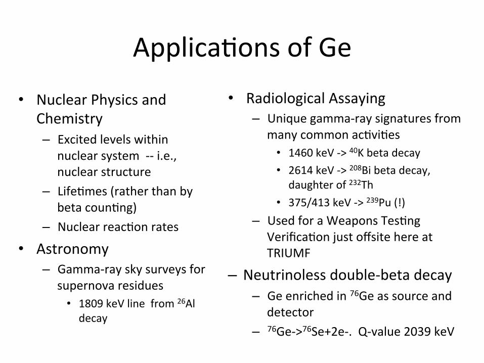
Job for an HPGe: The Shape of 10Be
2011-06-15 CAP Congress 2011, St. John's, NL 5
M22 > 0
M22 < 0
• Conven6onal wisdom: 10Be 0+gs, 2+1 prolate (M22>0)
• AV18 alone: 2+1 oblate, 2+2 prolate
• Include IL2 3-‐body forces: 2+1 prolate, 2+2 oblate
• Bonn NCSM: 2+1 prolate without 3-‐body forces

It’s a football

Job for an HPGe: finding trace “peacekeeper” radioac6ve isotopes

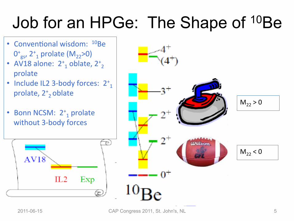
Job for an HPGe: Galac6c Structure • HPGe in Space • Look for gamma rays from centre
of galaxy • 1809 keV from 26Al
• COMPTEL, INTEGRAL
Job for an HPGe: Galac6c Structure

Making High-‐Purity Germanium • Crystal grown by “pulling” from molten Ge
– Czochralski technique – Seed crystal slowly withdrawn – Ge freezes to seed as single crystal
• Diameters up to ~11 cm achievable, but rare • 5-‐8 cm reasonable
– At phase interface, impuri6es “frozen out”, collect in liquid
– In prac6ce, “top” of crystal purer than “bo<om”
• “Zone Refining” – Pass through microwave oven – Melt “zone” migrates impuri6es one more 6me
• Resul6ng crystals: 1010 impuri6es per cm3

Typical Ge configura6on: Closed-‐End Coaxial
• Machining ater crystal forma6on – Right cylinder – Hole drilled partway through centre – Typical dimensions: Ro=2-‐7 cm, ℓ=4-‐12 cm,
ri=0.5 cm, x=1 cm • Contacts formed on outer (reddish) surface
(except top, as shown) and inner core (blueish) – n+ contact: drited Li (~0.1 cm) – p+ contact: implanted boron
(2 µm) • Placement of contact depends on bulk
– If bulk is slightly p-‐type: Li on outside • Thicker dead area on larger surface • Lower efficiency for very low-‐energy photons
– If bulk is slightly n-‐type: Li on core – N-‐ vs. P-‐type decision based on two factors:
• Price (p-‐type cheaper) • Neutron damage (n-‐type more resistant, easier to fix)
Ro
ℓ
x
ri
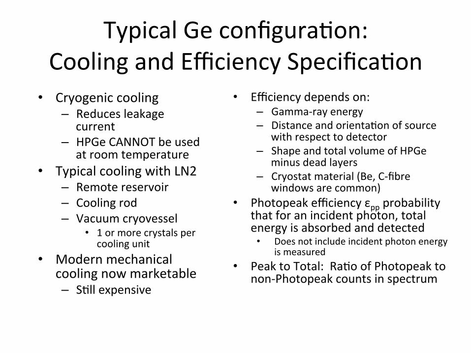
Typical Ge configura6on: Cooling and Efficiency Specifica6on
• Cryogenic cooling – Reduces leakage
current – HPGe CANNOT be used
at room temperature • Typical cooling with LN2
– Remote reservoir – Cooling rod – Vacuum cryovessel
• 1 or more crystals per cooling unit
• Modern mechanical cooling now marketable – S6ll expensive
• Efficiency depends on: – Gamma-‐ray energy – Distance and orienta6on of source
with respect to detector – Shape and total volume of HPGe
minus dead layers – Cryostat material (Be, C-‐fibre
windows are common) • Photopeak efficiency εpp probability
that for an incident photon, total energy is absorbed and detected
• Does not include incident photon energy is measured
• Peak to Total: Ra6o of Photopeak to non-‐Photopeak counts in spectrum

HPGe Efficiency Standard • Standard candle: 60Co gamma ray source 25
cm from front of CRYOSTAT – Oriented in front of any entry window
• Efficiency defined as photopeak counts from 1332 keV gamma ray, rela6ve to rela6ve to a 3 in x3 in NaI(Tl) cylinder
• 100% = 1.2x10-‐3 absolute • A 100% HPGe would be about 9 cm x 9
cm • Peak-‐to-‐total: ra6o of counts in 1332 and
1173 keV gamma rays versus total counts – Con6nuum from escaping energy
• Compton sca<ering out of Ge • Annihila6on photons escaping Ge • etc
– Manufacturers typically specify a lower limit of 150 keV for summing “total” counts
– Typical values 15% to 25%
1173 1332
Total

Two typical HPGe detectors (here at TRIUMF)
• Single-‐crystal p-‐type • 80% rela6ve to NaI • Used mainly for ISAC-‐I
decay spectroscopy
• TIGRESS Clovers • Four-‐crystal n-‐type, 40% each
– 8 segments on outer contact • ISAC-‐II in-‐beam spectroscopy
Coaxial crystal in here
Cold finger inside here
LN2 reservoir
Preamp, HV filter under here
4 tapered Coaxial crystals
Cold finger
LN2 reservoir
Preamp, HV filter under here

Typical Ge configura6on: Deple6on, Bias, Readout
• Deple6on voltage can be es6mated from impurity concentra6on, assume infinite coaxial “capacitor” with dielectric – Vd = (Ne/2ε)[ri2 ln (Ro/ri) – (1/2)(Ro2-‐ri2)] – N=(Na-‐Nd)=net density of “electronically ac6ve” impurites
(acceptors minus donors) – ε = permi~vity (ε/ε0=16.7 for HPGe) – Vd typically 1000 V to 4000 V in readily available detectors
• Typically operate HPGe as high as possible – 500 to 2000 V above deple6on – About 2000 V/cm field -‐-‐ Surprisingly uniform
• Charge-‐sensi6ve preamplifiers – Integrates induced current – Can place front-‐end FET and feedback network in cryostat to
improve resolu6on
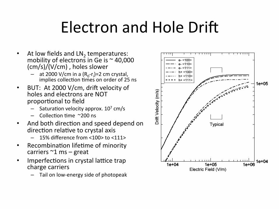
Electron and Hole Drit • At low fields and LN2 temperatures:
mobility of electrons in Ge is ~ 40,000 (cm/s)/(V/cm) , holes slower
– at 2000 V/cm in a (R0-‐ri)=2 cm crystal, implies collec6on 6mes on order of 25 ns
• BUT: At 2000 V/cm, drit velocity of holes and electrons are NOT propor6onal to field
– Satura6on velocity approx. 107 cm/s – Collec6on 6me ~200 ns
• And both direc6on and speed depend on direc6on rela6ve to crystal axis
– 15% difference from <100> to <111> • Recombina6on life6me of minority
carriers ~1 ms – great • Imperfec6ons in crystal la~ce trap
charge carriers – Tail on low-‐energy side of photopeak
13-‐03-‐01 17
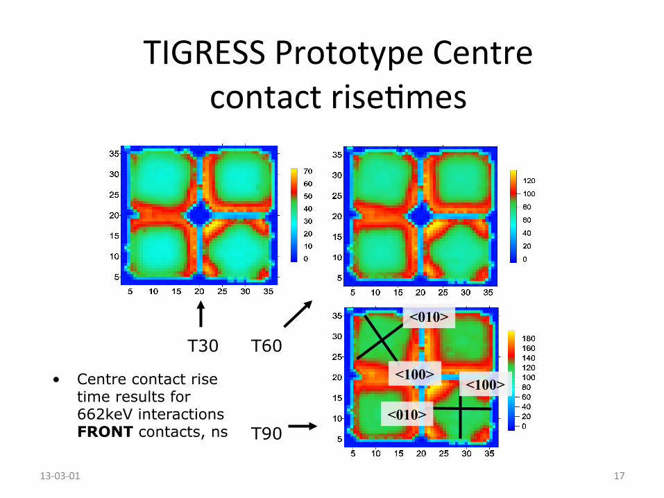
TIGRESS Prototype Centre contact rise6mes
• Centre contact rise time results for 662keV interactions FRONT contacts, ns
T30 T60
T90
<010>
<100> <100>
<010>

Neutron Damage • Neutron flux creates charge trapping
centres – Nuclear sca<ering can dislodge Ge
from crystal la~ce site • Consequence: incomplete charge
collec6on – Poor resolu6on – Low-‐energy tails
• Threshold for measurable effect depends on size, type.
– “Large” p-‐type (70%): 1x10⁷ neutrons/cm2
– “Large” n-‐type: 1x10⁹ neutrons/cm2 – Smaller detectors less suscep6ble
• Recoverable by annealing – P-‐type: weeks – N-‐type: days – Annealing may cause Li to drit,
causing efficiency loss • Worse for p-‐type
• Effect oten does not appear un6l bias removed and reapplied
• Deliberately damaged and annealed n-‐type detector
• 3x10⁹ neutrons/cm2 dose

Posi6on dependence of collected charge profile
• Consider core contact, n-‐type detector
– posi6ve voltage on Li inner core – Ro-‐ri ~ 2.5 cm – ve ~ 107 cm/s, vh ~ 0.75x107 cm/s – Space charge plus opera6ng
overvoltage results in nearly constant E-‐field for drit
– But Ramo weigh6ng Ew field for core propor6onal to 1/r
• Energy losses near core (A) – Electrons reach core immediately – Holes drit for 270 ns – Ini6al charge buildup on core (induced
current) large since Ew large – Rate of charge buildup decreases
• Energy loss near outside (B) – Holes reach outside immediately – Electrons drit for 200 ns – Induced current small ini6ally – Increases as electrons reach region of
high weigh6ng field near core
Charge , q (arb)
Time
270 ns
200 ns
h
e
A
B
Ew r
• BOTTOM LINE: Pulse shapes vary dras6cally based on loca6on of interac6on
– Mul6ple interac6ons : linear sum of currents
– Time resolu6on is poor.
V+
–
A
B

Posi6on dependence of induced charge profile
• Implanted contact may be easily segmented by masking during implanta6on
– Outer-‐contact segmenta6on common in modern (pure research) applica6ons
• Neighboring contacts collect no net charge • But induced currents give rise to a transient
pulse – Due to fringing in weigh6ng field
• Charge-‐carrier genera6on nearer to contact results in larger transient signal
• Polarity of pulse depend on whether nearer to core or outside
– Certain loca6ons: induced currents cancel, transient pulses negligible
• Compton cameras and tracking arrays analyse pulse shapes to localize interac6ons, reconstruct source incoming vector
– Example here: Compton sca<ering followed by photoabsorp6on
+
q
t
q
t q
t
(schema6c)
• Posi6on sensi6vity depends on segment geometry, noise
• 2 mm for single interac6ons demonstrated in TIGRESS

Addback and Escape Suppression • If all incoming photon
energy is deposited in crystal, you get a high resolu6on photopeak
• High probability that a Compton sca<er or annihila6on photon following pair produc6on will escape
• Lost energy has a con6nuous spectrum
• Becomes a background that can swamp weak lines
• Solu6ons: • Place HPGe detectors in
close proximity and add energy loss in each – E.g. TIGRESS clover
• Surround HPGe with less expensive, high density scin6llator – BGO works well: X0=1.1 cm – Veto events with BGO signal
in coincidence with HPGe signal
– Leave entrance hole of course

Addback and Escape Suppression
• TIGRESS HPGe crystal and suppressor scheme
• Suppression: If energy measured in front, side or back scin6llators, veto any events in HPGe
û
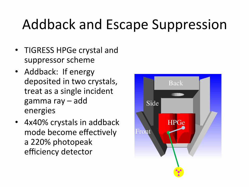
Addback and Escape Suppression • TIGRESS HPGe crystal and
suppressor scheme • Addback: If energy
deposited in two crystals, treat as a single incident gamma ray – add energies
• 4x40% crystals in addback mode become effec6vely a 220% photopeak efficiency detector

60Co – Full Suppression

60Co – Full Suppression

60Co – Full Suppression

0 2000 4000 6000 8000100
1000
10000
100000
Count
s
Energy (keV)
Addback Add
0 2000 4000 6000 800010
100
1000
10000
Counts
Energy (keV)
Unsuppressed single core Fully suppressed single core
Fully suppressed data for a single TIGRESS detector
11Be β decay (t1/2 = 13.8 s) gives gamma-‐rays up to 8 MeV
Characterising TIGRESS for high energy – R. Kshetri, SFU/TRIUMF
Life6mes, Matrix Elements 10Be -‐-‐ LBNL

7000 7500 8000
50
100
150
Unsuppressed single core Suppressed single core
Cou
nts
Energy (keV)7000 7200 7400 7600 7800 8000
200
400
600
800
Double escape peak
Single escape peak
Energy = 7974.73 keV
FWHM (addbk) = 9.48 keVFWHM (add) = 8.91 keVArea (Addback) = 6978 (98)
Area (Add) = 3298 (62)so, Addback factor at 8 MeV = 2.12 (5)
Cou
nts
Energy (keV)
Addback Add
Cou
nts
Life6mes, Matrix Elements 10Be -‐-‐ LBNL
TIGRESS Addback, Suppression

Life6mes, Matrix Elements 10Be -‐-‐ LBNL
TIGRESS absolute efficiency for 12C, 10Be Campaign
n 8 clovers and fixed side & back suppressors
n 12 sets of retractable front shields
n Maximum suppresson configura6on n Clovers back n Suppressors
forward

Other Ge configura6ons • Planar detectors
– 5 to 20 mm thick hockey pucks – Superior low-‐energy response – Varia6on: Low-‐Ax
• Double-‐Sided Strip HPGe – Square, with orthogonal strips on
opposite sides – Choice for Compton cameras
(medical, security imaging) • Ge(Li)
– Before HPGe – Use heat, electric field to drit Li
donors into bulk to compensate acceptor impuri6es
– “Freeze” Li in place at opera6ng temparature
– If these warm up they are destroyed.

Other Ge configura6ons • “Drit Chamber” HPGe • Replace core with “bu<on” • Induced signal on bu<on
only when electrons very close – Weigh6ng field propor6onal
to 1/r2
• Clean iden6fica6on of mul6-‐site vs. single-‐site energy deposi6on – Will be used in Majorana to
discriminate neur6noless double-‐beta decay from high-‐energy gamma ray pair produc6on

Up and coming alterna6ves to HPGe
Cadmium Zinc Teluride • Semiconductor • Room temperature
opera6on • About twice the FWHM • Crystal growth is s6ll
challenging • Holes very slow (1/10th
electron) and easily trapped • Appropriate for imaging
applica6ons
LaBrCe • Scin6llator • Room temperature • About twice the FWHM • Excellent 6ming
– 3 ns light curve • Patented -‐> expensive • Compe66ve for in-‐beam
spectroscopy

The end
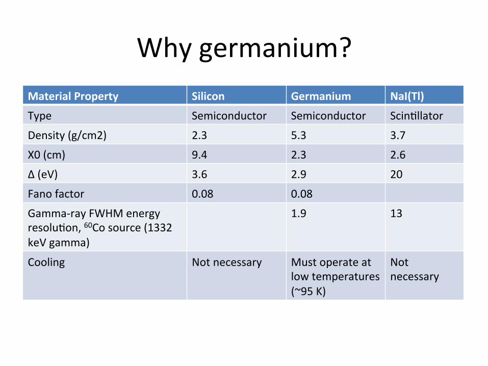
Why germanium? Material Property Silicon Germanium NaI(Tl)
Type Semiconductor Semiconductor Scin6llator
Density (g/cm2) 2.3 5.3 3.7
X0 (cm) 9.4 2.3 2.6
Δ (eV) 3.6 2.9 20
Fano factor 0.08 0.08
Gamma-‐ray FWHM energy resolu6on, 60Co source (1332 keV gamma)
1.9 13
Cooling Not necessary Must operate at low temperatures (~95 K)
Not necessary