Embed Size (px)
Citation preview

PHOTONIC SENSORS / Vol. 7, No. 2, 2017: 182‒192
Modeling of All-Optical Even and Odd Parity Generator Circuits Using Metal-Insulator-Metal Plasmonic Waveguides
Lokendra SINGH, Amna BEDI, and Santosh KUMAR*
Photonics Lab, Department of Electronics and Communication Engineering, DIT University, Dehradun-248009, India *Corresponding author: Santosh KUMAR E-mail: [email protected]
Abstract: Plasmonic metal-insulator-metal (MIM) waveguides sustain excellent property of confining the surface plasmons up to a deep subwavelength scale. In this paper, linear and S-shaped MIM waveguides are cascaded together to design the model of Mach-Zehnder interferometer (MZI). Nonlinear material has been used for switching of light across its output ports. The structures of even and odd parity generators are projected by cascading the MZIs. Parity generator and checker circuit are used for error correction and detection in an optical communication system. Study and analysis of proposed designs are carried out by using the MATLAB simulation and finite-difference- time-domain (FDTD) method.
Keywords: Plasmonics; MIM waveguides; Mach-Zehnder interferometer; nonlinear process; FDTD method
Citation: Lokendra SINGH, Amna BEDI, and Santosh KUMAR, “Modeling of All-Optical Even and Odd Parity Generator Circuits Using Metal-Insulator-Metal Plasmonic Waveguides,” Photonic Sensors, 2017, 7(2): 182–192.
1. Introduction
In today’s scenario of photonic industry, the
major challenge is the miniaturization of optical
components for wavelength division multiplexing
[1]. Despite the deep subwavelength confinement of
surface plasmon polaritons (SPPs) with respect to
other nanophotonic waveguides such as photonic
crystals, SPP waveguides work well beyond the
diffraction limit [2‒4]. Plasmonics is one of the
promising fields of integrated photonics due to its
numerous applications in optical clocking, cancer
therapy, nano-lithography, solar cells, etc. In
designing of building blocks for future generation of
integrated optical components and devices,
plasmonic waveguides play a significant role.
Recently, several types of waveguides were
discovered such as slots [5, 6], plasmonic wedge
waveguide [7], and dielectric ridge on the metal
surface [8], but among all these waveguides the
metal-insulator-metal (MIM) waveguide is generally
preferred due to its their exceptional property of
confining the surface plasmons to a deep
subwavelength scale [9‒13]. In these waveguides,
propagation is achieved by using even modes due to
their low-loss confinement profile. Considering the
photonic device altogether, directional couplers
(DCs) are serves as a prime component to design the
elementary part of optical circuits. Recently, several
designs of directional couplers have been proposed
by using plasmonic waveguides [14‒17]. The major
phenomenon of coupling of light within the DC is
beating of even-odd modes. As the equal splitting of
power through the directional coupler is wavelength
dependent, for broadband response either
wavelength dependency should be removed by
Received: 20 July 2016 / Revised: 16 November 2016 © The Author(s) 2017. This article is published with open access at Springerlink.com DOI: 10.1007/s13320-017-0365-9 Article type: Regular

Lokendra SINGH et al.: Modeling of All-Optical Even and Odd Parity Generator Circuits Using Metal-Insulator-Metal Plasmonic Waveguides
183
making coupler adiabtic, or input power with its
coupling length should be controlled. In the
proposed structure of DC connected in the
Mach-Zehnder interferometer (MZI), equal splitting
of power is attained with coupling length and
propagation length of 1 m and 10.2 m,
respectively. Hence, by adjoining the two DCs using
two linear MIM waveguides, a design of MZI has
been designed within the footprints of (16.24) m.
Although interferometric circuit using Fabry-Perot
interferometer is also used in various applications,
the need of too many sources will lead to an increase
in the cost and complexity of devices [18]. One of
the arms of MZI is filled with an active material.
Here, MEH-PPV [poly (2-methoxy-5-
(28-ethylexyloxy)-PPV)] is used as an active
material with refractive index and response time of
n=1.65 and =2.le15 s, respectively [19]. The
presence of active materials in the structure of MZI
is used to switch the light across its output ports by
changing the refractive index of waveguide with
respect to power of input signals. The changes in
phase canceling out or adding each other depend on
nonlinear processes. If phase of both the signals
cancels out each other then it crosses phase
modulation (XPM), and if it adds then it is self
phase modulation (SPM). Due to XPM, the optical
signal arrives at through port and SPM thrives the
signal at cross port of MZI. Thus, by cascading
plasmonic DCs and MZIs, all-optical structures of
even and odd parity generators are modeled within
the footprints of (12510) m and (20510) m,
respectively. Recently, some switching circuits have
been proposed by using LiNbO3-based MZI, which
work on the principle of electro-optic effect [20].
Although the work is excellent, it still lacks
advanced applications in terms of device
miniaturization up to a deep subwavelength scale
(hence overall design of device remains in thousand
of micrometers), and due to the presence of
electrical signals for altering the refractive index of
waveguides, it limits the speed of device. Some
switching circuits were also proposed by using
semiconductor optical amplifier (SOA) but they
were backsitted due to the phenomenon of gain
saturation [21]. All optical logic gates were also
proposed using photonic crystal but being lack of
the nonlinear material inside the structure will
enable the switching of optical signals for complex
circuits [22].
The proposed design of parity generators are
verified by using the finite difference time domain
(FDTD) method [23] and MATLAB simulation.
Section 2 presents the models of even and odd parity
generators with their mathematical formulations. In
Section 3, the propagation of light through proposed
structures is projected. Finally, the conclusions of
complete work are presented in Section 4.
2. Design of parity generator circuits
The combinational circuits are useful in
designing various integrated circuits which are very
useful in micro-controlling and central processing
units. In this work, for designing the all optical
circuits of parity generators, MIM plasmonic
waveguides are used. To create the MIM geometry, a
metal (SiON) having high refractive index of
1 2.01n with permittivity of 1+j2.9 is deposited
over a low index substrate having refractive index of
2 1.44n , and air is considered as dielectric between
them. The thickness of dielectric is taken as 0.5 m
for the propagation of surface plasmons with a
propagation length of 10.2 m. Thus by using these
MIM waveguides, the structure of MZI is designed
as shown in Fig. 1, whose second linear arm is filled
with nonlinear Kerr or active material. When the
optical signals with power of Ein=0.014 W/m
(considered as digital logic “0”) are given at the first
input port, then by obeying the phenomenon of SPM,
signals are obtained at the second output port of
MZI as shown in Fig. 2(a). When signals with the
power Ein=0.081W/m (considered as digital logic
“1”) are incident at the first input port of MZI, then

Photonic Sensors
184
due to XPM optical signals arrive at the first output
port of it as shown in Fig. 2(b). The extinction ratio
(ER) of single MZI is about 26 dB at output power
difference of 0.7 dB and 0.8 dB. The analyzed value
of ER for single MZI is quite useful and enough for
designing the all-optical logic gates [24].
Fig. 1 Schematic of single Mach-Zehnder interferometer.
Input signal
Output port l
Output port 2
(a)
(b)
Fig. 2 Propagation of light through single MZI: (a) for low intensity signals and (b) for high intensity signals.
Thus, this toggling of optical signals across
output ports of MZI with respect to input power of
source is mathematically written as [25‒28]
2out1 insin 0.014 W/μm
2T atE
(1)
2out2 incos 0.081 W/μm
2T atE
(2)
where is the total change in phase in two linear
arms of MZI. Equations (1) and (2) represent the
mathematical expressions for outputs of MZI when
input is fed with high and low powers, respectively.
2.1 Even parity generator
Figure 3 shows the digital circuit and K-map of three bit even parity generators, and Table 1 presents the truth table of the even parity generator. The circuit of the even parity generator is designed by cascading six MZIs and four directional couplers as shown in Fig. 4. For the proper functioning of device,
three optical sources are placed in front of the second input ports of MZI1, MZI2, and MZI3. Three directional couplers DC1, DC2, and DC3 for splitting the optical energy into two equal parts are connected at the second output port of all three MZIs, respectively. The second output ports of DC1 and DC2 are combined together with the first output port of DC3 to feed the MZI5. While the first output ports of DC1 and DC2 are combined together to feed the MZI4 at the second input port DC4 is connected at the second output port of same MZI. Then the second output ports of DC3 and DC4 are combined together to feed MZI6 at its first input port. Finally, the second and first output ports of MZI5 and MZI6 are combined together to get the required output of even parity generator.
Fig. 3 Digital circuit and K-map of three bit even parity
generator circuit.

Lokendra SINGH et al.: Modeling of All-Optical Even and Odd Parity Generator Circuits Using Metal-Insulator-Metal Plasmonic Waveguides
185
Fig. 4 Schematic diagram of even parity generator.
Table 1 Truth table of even parity generator.
Input signals Output signals Min-terms
A B C EP
1m 0 0 0 0
2m 0 0 1 1
3m 0 1 0 1
4m 0 1 1 0
5m 1 0 0 1
6m 1 0 1 0
7m 1 1 0 0
8m 1 1 1 1
In Fig. 1, the power at the output of directional
coupler towards the input side can be written as [24]
2sinAP L
2cosBP L (3)
where is the attenuation constant of DC towards
input side, and L is its coupling length which is 1 m.
Thus, by using (1)‒(3), mathematical expressions for
the output of even parity generator circuit can be
written as
2 2 2 MZI3MZI1 MZI21 cos cos cos
2 2 2m
(4)
2 2MZI1 MZI22 cos cos
2 2m
2 2 2MZI3 MZI5DC3sin sin cos
2 2L
(5)
2 2 2MZI1 MZI23 DC2cos sin cos
2 2m L
×
2 2MZI5 MZI3cos cos2 2
(6)
2 MZI14 cos
2m
2 2MZI2DC2
2 MZI5
2 2MZI3DC3
sin cos2
sin2
sin sin2
L
L
(7)
2 2 2 MZI5MZI15 DC1sin cos cos
2 2m L
2 2 MZI3MZI2cos cos2 2
(8)
2 2MZI1DC1
2 MZI56
2 2MZI3DC3
sin cos2
sin2
sin sin2
L
m
L
2 MZI2cos2
(9)
2 2MZI1DC1
2 MZI57
2 2MZI2DC2
sin cos2
sin2
sin cos2
L
m
L
2 MZI3cos2
(10)
8
2 2MZI1DC1
2 2MZI2DC2
sin sin2
sin sin2
m
L
L
×
2 2MZI4DC2
2 MZI6
2 2MZI3DC3
sin cos2
sin2
sin cos2
L
L
.
Thus, overall output of even parity generator (EPG)

Photonic Sensors
186
can be written as EPG 2 3 5 8OUT m m m m , since
there is no signal at output ports for the rest of min-terms.
The timing diagram of even parity generator
through MATLAB is presented in Fig. 5, which is
verified by its truth table given in Table 1.
Fig. 5 Timing diagram of even parity generator through MATLAB.
In Fig. 5, the first three rows present the timing
sequence for input optical signals, and the fourth
row presents the timing signals for the output of
parity generator. In the timing diagram, signals in
the fourth row with higher magnitudes represent the
presence of signal at output, while signals with
lower magnitude show absence of signal.
2.2 Odd parity generator
Figure 6 shows a digital circuit and K-map of a
three-bit-odd-parity generator, and Table 2 presents
the truth table of odd parity generator. The design of
an odd-parity generator is obtained by cascading
seven MZIs and five DCs as shown in Fig. 7.
Fig. 6 Digital circuit and K-map of a three-bit-odd-parity generator.
Fig. 7 Block diagram of odd parity generator.
Input optical signals are given at the second, first
and second input ports of MZI1, MZI2, and MZI3,
respectively. DC1 and DC2 are connected at the
second and first output ports of MZI1 and MZI2,

Lokendra SINGH et al.: Modeling of All-Optical Even and Odd Parity Generator Circuits Using Metal-Insulator-Metal Plasmonic Waveguides
187
respectively. The second and first output ports of
MZI2 and MZI3 are cobbled together to feed the
MZI4 with optical signals at its second input port,
while the second and first output ports of DC1 and
MZI4 are combined together to feed MZI5 at its
second input port. To feed MZI6 at its first input
port, the first output ports of MZI1 and DC5 (which
is connected at the second output port of MZI4) are
combined together. The second and first output ports
of DC2 and DC3 (which is connected at the second
output port of MZI3) are combined together to feed
DC4, whose first output port is combined with the
second output port of MZI6 to feed the MZI7.
Finally, to get the output of odd parity generator, the
first output ports of MZI6 and MZI7 are combined
together with the second output port of MZI5.
The mathematical expression for outputs of odd
parity generator circuit using (1)‒(3) can be written
as
2 MZI2
2 MZI1
2 2MZI3 MZI61
2 2MZI4DC5
cos2
cos2
cos sin2 2
sin sin2
m
L
2
2 2 MZI6MZI1
2 2 2MZI3DC3 DC4
cos cos2 2
sin sin sin2
m
L L
×
2 2MZI7 MZI2
2 2 MZI5MZI4
cos cos2 2
cos cos2 2
3
2 2 MZI6MZI1
2 2 2MZI2DC2 DC4
2 2MZI7 MZI3
2 2 MZI5MZI4
cos cos2 2
sin sin sin2
cos cos2 2
cos cos2 2
L
m
L
2 2 MZI6MZI1
2 2MZI2DC2
2 MZI7
2 2MZI3DC
4
3
2DC4
cos cos2 2
sin sin2
sin2
sin sin2
sin
L
L
L
m
52 2 2 MZI5MZI1
DC1
2 2 MZI3MZI2
2 2MZI4DC5
2 2MZI6 MZI7
sin cos cos2 2
cos cos2 2
sin sin2
cos cos2 2
Lm
L
6
2 2MZI1DC1
2 MZI5
2 2MZI2 MZI4
2 2MZI3DC3
2 2 MZI7DC4
sin cos2
sin2
cos cos2 2
sin sin2
sin cos2
L
L
L
m
7
2 2MZI1DC1
2 2MZI3 MZI4
sin cos2
cos cos2 2
m
L
2 2 2MZI5 MZI2DC2
2 2 MZI7DC4
sin sin sin2 2
sin cos2
L
L
82 2 2 MZI5MZI1
DC1
2 2MZI2DC2
2DC3
2 2MZI3DC3
2 2 2MZI7 MZI2DC2
2DC4
sin cos cos2 2
sin sin2
sin
sin sin2
cos sin sin2 2
sin cos
L
L
L
L
L
L
m
2 MZI7
2

Photonic Sensors
188
Table 2 Truth table of odd parity generator.
Input signals Output signals Min-terms
A B C OP
1m 0 0 0 1
2m 0 0 1 0
3m 0 1 0 0
4m 0 1 1 1
5m 1 0 0 0
6m 1 0 1 1
7m 1 1 0 1
8m 1 1 1 0
Thus, the overall output of odd parity generator
(OPG) is written as OPG 1 4 6 7OUT m m m m ,
since there is no optical signal at the output port for
the rest of min-terms. The timing diagram of the odd parity generator
through MATLAB is presented in Fig. 8, which is verified by its truth table given in Table 2. In Fig. 8, the first three rows represent the timing signals for input signals, and the fourth row represents the timing signals for the generated output of the odd parity generator, which is truly matched with its truth table. In timing diagram at the fourth row, timing signals with low and high magnitudes only represent the presence and absence of optical signals at the desired output.
1 2 3 4 5 6 7 8 0
Time (s)
1.00.50
Opt
ical
sig
nal
(A)
Opt
ical
sig
nal
(B)
Opt
ical
sig
nal
(C)
Odd
par
ity
gene
rato
r
1 2 3 4 5 6 7 8 0
Time (s)
1.00.50
1 2 3 4 5 6 7 8 0
Time (s)
1.00.50
1 2 3 4 5 6 7 8 0
Time (s)
1.00.50
Fig. 8 Timing diagram of odd parity generator.
3. Simulation results using FDTD
The finite difference time domain (FDTD)
method has been used for analysis of propagation of
optical signals through the design of parity generator
circuits, and their verifications are done by using
MATLAB. The continuous wave (CW) source is
used to provide the input signals with Gaussian
distribution under the transverse magnetic (TM)
polarization at the wavelength of 1550 nm. The
Gaussian distribution of signals spectrum is very
useful because the interference occurs with side
lobes of spectrum, while the maximum information
is transmitted on the peak lobe which remains
unaffected. For the simulation of the proposed
device, perfect matched layers are considered as
boundary layers for all interfaces of metal and
dielectric with 121e as reflection coefficient. The
half width of input source is 0.39 m within the
mesh size of x=0.021 m and z=0.051 m, under
the perfect matched layer (PML) as boundary
conditions for all interfaces of metal and dielectric.
3.1 Simulation results of even parity generator
The simulation result of propagation of light
through the even parity generator with combination
of all possible input signals is presented in Fig. 9.
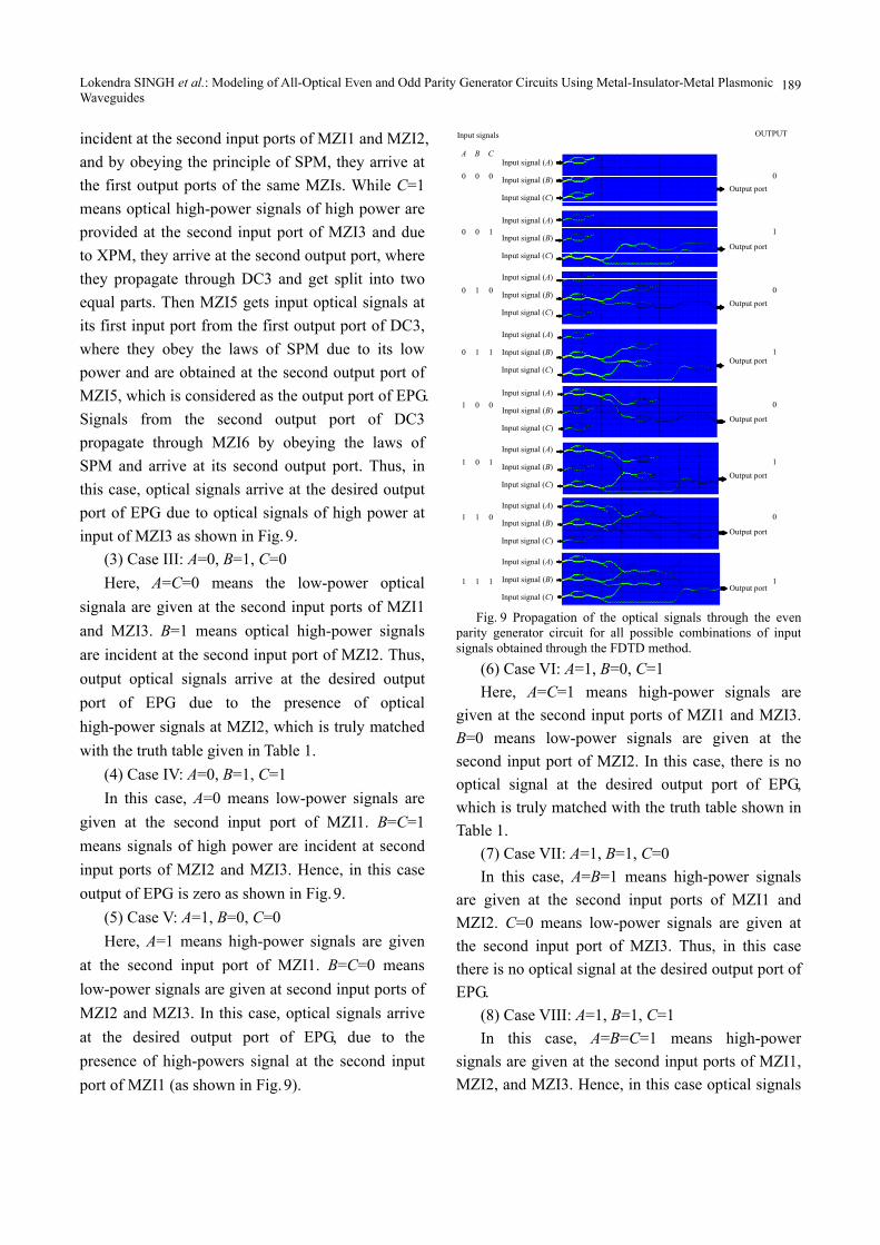
(1) Case I: A=0, B=0, C=0
In this case, A=B=C=0 means all three input
ports are fed with optical signals having low input
power, and thus by following the phenomenon of
SPM, these signals are obtained at the first output
ports of MZI1, MZI2, and MZI3. Hence, there is no
signal at the output port of the even parity generator
as shown in Fig. 9, which is truly matched with its
truth table given in Table 1.
(2) Case II: A=0, B=0, C=1
Here, A=B=0 means low-power signals are
Lokendra SINGH et al.: Modeling of All-Optical Even and Odd Parity Generator Circuits Using Metal-Insulator-Metal Plasmonic Waveguides
189
incident at the second input ports of MZI1 and MZI2,
and by obeying the principle of SPM, they arrive at
the first output ports of the same MZIs. While C=1
means optical high-power signals of high power are
provided at the second input port of MZI3 and due
to XPM, they arrive at the second output port, where
they propagate through DC3 and get split into two
equal parts. Then MZI5 gets input optical signals at
its first input port from the first output port of DC3,
where they obey the laws of SPM due to its low
power and are obtained at the second output port of
MZI5, which is considered as the output port of EPG.
Signals from the second output port of DC3
propagate through MZI6 by obeying the laws of
SPM and arrive at its second output port. Thus, in
this case, optical signals arrive at the desired output
port of EPG due to optical signals of high power at
input of MZI3 as shown in Fig. 9.
(3) Case III: A=0, B=1, C=0
Here, A=C=0 means the low-power optical
signala are given at the second input ports of MZI1
and MZI3. B=1 means optical high-power signals
are incident at the second input port of MZI2. Thus,
output optical signals arrive at the desired output
port of EPG due to the presence of optical
high-power signals at MZI2, which is truly matched
with the truth table given in Table 1.
(4) Case IV: A=0, B=1, C=1
In this case, A=0 means low-power signals are
given at the second input port of MZI1. B=C=1
means signals of high power are incident at second
input ports of MZI2 and MZI3. Hence, in this case
output of EPG is zero as shown in Fig. 9.
(5) Case V: A=1, B=0, C=0
Here, A=1 means high-power signals are given
at the second input port of MZI1. B=C=0 means
low-power signals are given at second input ports of
MZI2 and MZI3. In this case, optical signals arrive
at the desired output port of EPG, due to the
presence of high-powers signal at the second input
port of MZI1 (as shown in Fig. 9).
A
0
0
0
0
1
1
1
1
0
0
1
1
0
0
1
1
B
0
1
0
1
0
1
0
1
CInput signal (A)
Input signal (B)
Input signal (C)Output port
Input signal (A)
Input signal (B)
Input signal (C)Output port
Input signal (A)
Input signal (B)
Input signal (C)Output port
Input signal (A)
Input signal (B)
Input signal (C)Output port
Input signal (A)
Input signal (B)
Input signal (C)Output port
Input signal (A)
Input signal (B)
Input signal (C)Output port
Input signal (A)
Input signal (B)
Input signal (C)Output port
Input signal (A)
Input signal (B)
Input signal (C)Output port
0
1
0
1
0
1
0
1
OUTPUTInput signals
Fig. 9 Propagation of the optical signals through the even
parity generator circuit for all possible combinations of input signals obtained through the FDTD method.
(6) Case VI: A=1, B=0, C=1
Here, A=C=1 means high-power signals are
given at the second input ports of MZI1 and MZI3.
B=0 means low-power signals are given at the
second input port of MZI2. In this case, there is no
optical signal at the desired output port of EPG,
which is truly matched with the truth table shown in
Table 1.
(7) Case VII: A=1, B=1, C=0
In this case, A=B=1 means high-power signals
are given at the second input ports of MZI1 and
MZI2. C=0 means low-power signals are given at
the second input port of MZI3. Thus, in this case
there is no optical signal at the desired output port of
EPG.
(8) Case VIII: A=1, B=1, C=1
In this case, A=B=C=1 means high-power
signals are given at the second input ports of MZI1,
MZI2, and MZI3. Hence, in this case optical signals
Photonic Sensors
190
are obtained at the desired port of EPG, which is
truly matched with its truth table.
3.2 Simulation results odd parity generator
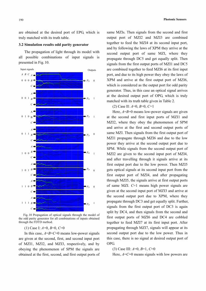
The propagation of light through its model with
all possible combinations of input signals is
presented in Fig. 10.
A
0
0
0
0
1
1
1
1
0
0
1
1
0
0
1
1
B
0
1
0
1
0
1
0
1
C
Input signals
0
1
1
0
1
0
0
1
A
B
C
A
B
C
A
B
C
A
B
C
A
B
C
A
B
C
A
B
C
A
B
C
PO
PO
PO
PO
PO
PO
PO
PO
Outputs
Fig. 10 Propagation of optical signals through the model of
the odd parity generator for all combinations of inputs obtained through the FDTD method.
(1) Case I: A=0, B=0, C=0
In this case, A=B=C=0 means low-power signals
are given at the second, first, and second input port
of MZI1, MZI2, and MZI3, respectively, and by
obeying the phenomenon of SPM the signals are
obtained at the first, second, and first output ports of
same MZIs. Then signals from the second and first
output port of MZI2 and MZI3 are combined
together to feed the MZI4 at its second input port,
and by following the laws of XPM they arrive at the
second output port of same MZI, where they
propagate through DC5 and get equally split. Then
signals from the first output ports of MZI1 and DC5
are combined together to feed MZI6 at its first input
port, and due to its high power they obey the laws of
XPM and arrive at the first output port of MZI6,
which is considered as the output port for odd parity
generator. Thus, in this case an optical signal arrives
at the desired output port of OPG, which is truly
matched with its truth table given in Table 2.
(2) Case II: A=0, B=0, C=1
Here, A=B=0 means low-power signals are given
at the second and first input ports of MZI1 and
MZI2, where they obey the phenomenon of SPM
and arrive at the first and second output ports of
same MZI. Then signals from the first output port of
MZI1 propagate through MZI6 and due to the low
power they arrive at the second output port due to
SPM. While signals from the second output port of
MZI2 are given to the second input port of MZI4,
and after travelling through it signals arrive at its
first output port due to the low power. Then MZI5
gets optical signals at its second input port from the
first output port of MZI4, and after propagating
through MZI5, the signals arrive at first output ports
of same MZI. C=1 means high power signals are
given at the second input port of MZI3 and arrive at
the second output port due to XPM, where they
propagate through DC3 and get equally split. Further,
signals from the first output port of DC3 is again
split by DC4, and then signals from the second and
first output ports of MZI6 and DC4 are cobbled
together to feed MZI7 at its first input port. After
propagating through MZI7, signals will appear at its
second output port due to the low power. Thus in
this case, there is no signal at desired output port of
OPG.
(3) Case III: A=0, B=1, C=0
Here, A=C=0 means signals with low powers are

Lokendra SINGH et al.: Modeling of All-Optical Even and Odd Parity Generator Circuits Using Metal-Insulator-Metal Plasmonic Waveguides
191
incident at the second input ports of MZI1 and MZI3.
B=1 means high-power signals are given at the first
input port of MZI2. Thus, in this case there is no
optical signal at the desired output port of OPG.
(4) Case IV: A=0, B=1, C=1
Here, A=0 means the second input port of MZI1.
B=C=1 means high intensity signals are given at the
first and second input ports of MZI2 and MZI3.
Hence, in this case optical signals are obtained at the
desired output port of OPG, which is truly matched
with its truth table.
(5) Case V: A=1, B=0, C=0
In this case, A=1 means signals with high power
are given at the second input port of MZI1. B=C=0
means low-power signals are given at the first and
second input ports of MZI2 and MZI3. Thus, in this
case there is no optical signal at desired output port
of OPG.
(6) Case VI: A=1, B=0, C=1
Here, A=C=1 means the second input ports of
MZI1 and MZI3 are fed with high-power signals.
B=0 means low-power signals are incident at the
first input port of MZI2. Thus, in this case optical
signals arrive at the desired output port of OPG,
which is truly matched with the truth table given in
Table 2.
(7) Case VII: A=1, B=1, C=0
Here, A=B=1 means high-power signals are
given at the second and first input ports of MZI1 and
MZI2. C=0 means low-power signals are fed at the
second input port of MZI3. Finally, output signals
approach to the port which is assigned as output port
for OPG.
(8) Case VIII: A=1, B=1, C=1
Here, as A=B=C=1 means high-power signals
are given at the second, first, and second input ports
of MZI1, MZI2, and MZI3. Thus, in this case there
is no optical signal at desired output port of OPG.
4. Conclusions
In this paper, models of even and odd parity
generator are projected by using MIM plasmonic
waveguides due to their enormous capability of
confining the surface plasmons up to a deep
subwavelength scale. The concept of nonlinear MZI
using MIM plasmonic waveguides has been used to
cascade the desired structures. The proposed concept
of cascading the MZIs is useful for integrating the
all-optical devices. The circuits of parity generators
are mainly used for error detection and correction in
optical communication networks.
Open Access This article is distributed under the terms of the Creative Commons Attribution 4.0 International License (http://creativecommons.org/licenses/by/4.0/), which permits unrestricted use, distribution, and reproduction in any medium, provided you give appropriate credit to the original author(s) and the source, provide a link to the Creative Commons license, and indicate if changes were made.
References
[1] W. Wei, X. Zhang, and X. Ren, “Asymmetric hybrid plasmonic waveguide with centimetric scale propagation length under subwavelength confinement for photonic components,” Nanoscale Research Letters, 2014, 9(1): 1‒8.
[2] W. L. Barnes, A. Dereux, and W. E. Thomas, “Surface plasmon subwavelength optics,” Nature, 2003, 424(6950): 824‒830.
[3] D. K. Gramotnev and S. I. Bozhelvonyi, “Plasmonics beyond the diffraction limit,” Nature Photonics, 2010, 4(2): 83‒91.
[4] Y. Chen and H. Ming, “Review of surface plasmon resonance and localized surface plasmon resonance sensor,” Photonic Sensors, 2012, 2(1): 37‒49.
[5] G. Veronis and S. H. Fan, “Guided subwavelength plasmonic mode supported by a slot in a thin metal film,” Optics Letters, 2005, 30(24): 3359‒3361.
[6] L. Liu, H. Zhanghua, and H. Sailing, “Novel surface plasmon waveguide for high integration,” Optics Express, 2015, 13(17): 6645‒6650.
[7] A. Boltasseva, S. V. Valentyn, B. N. Rasmus, M. Esteban, G. R. Sergio, and I. B. Sergey, “Triangular metal wedges for subwavelength plasmon polariton guiding at telecom wavelengths,” Optics Express, 2008, 16(8): 5252‒5260.
[8] A. Kumar, J. Gosciniak, V. S. Volkov, S. Papaioannou, D. Kalavrouziotis, K. Vyrsokinos, et al., “Dielectric-loaded plasmonic waveguide components: going practical,” Laser & Photonics Reviews, 2013, 7(6): 938‒951.

Photonic Sensors
192
[9] W. L. Barnes, A. Dereux, and T. W. Ebbeen, “Surface plasmon subwavelength optics,” Nature, 2003, 424(6950): 824‒830.
[10] R. Charbonneau, N. Lahoud, G. Mattiussi, and P. Berini, “Demonstration of integrated optics elements based on long-ranging surface plasmon polaritons,” Optics Express, 2005, 13(3): 977‒984.
[11] L. Liu, Z. Han, and S. He, “Novel surface plasmon waveguide for high integration,” Optics Express, 2005, 13(17): 6645‒6650.
[12] J. A. Dionne, L. A. Sweatlock, H. A. Atwater, and A. Polman, “Plasmon slot waveguides: towards chip-scale propagation with subwavelength scale localization,” Physical Review B, 2006, 73(3): 035407-9.
[13] G. Veronis and S. Fan, “Modes of subwavelength plasmonic slot waveguides,” Journal of Lightwave Technology, 2007, 25(9): 2511‒2521.
[14] F. Lou, Z. Wang, D. Dai, L. Tylen, and L. Wousnski, “Experimental demonstration of ultra-compact directional couplers based on silicon hybrid plasmonic waveguides,” Applied Physics Letters, 2012, 100(24): 241105-1‒241105-4.
[15] M. Z. Alam, J. N. Caspers, J. S. Aitchison, and M. Mojahedi, “Compact low loss and broadband hybrid plasmonic directional coupler,” Optics Express, 2013, 21(13): 16029‒16034.
[16] D. K. Gramotnev, K. C. Vernon, and D. F. P. Pile, “Directional coupler using gap plasmon waveguides,” Applied Physics B, 2008, 93(1): 99‒106.
[17] Q. Li, Y. Song, G. Zhou, Y. Su, and M. Qiu, “Asymmetric plasmonic-dielectric coupler with short coupling length, high extinction ratio, and low insertion loss,” Optics Letters, 2010, 35(19): 3153‒3155.
[18] P. Jia, G. Fang, and D. Wang, “Characterization of miniature fiber-optic Fabry-Perot interferometric sensors based on hollow silica tube,” Photonic Sensors, 2016, 6(3): 193‒198.
[19] M. A. Bader, G. Marowsky, A. Bahtiar, K. Koynov, C. Bubeck, H. Tillmann, et al., “Poly (p-phenylenevinylene) derivatives: new promising materials for nonlinear all-optical waveguide switching,” Journal of the Optical Society of America B, 2002, 19(9): 2250‒2262.
[20] S. Kumar, Chanderkanta, and A. Amphawan, “Design of parity generator and checker circuit using electro-optic effect of Mach-Zehnder interferomenters,” Optics Communications, 2016, 364: 195‒224.
[21] L. Wang, Y. Wang, C. Wu, and F. Wang, “All-optical flip-flop based on coupled SOA-PSW,” Photonic Sensors, 2016, 6(4): 366‒371.
[22] X. S. Christina and A. P. Kabilan, “Design of optical logic gates using self-collimated beams in 2d photonic crystal,” Photonic Sensors, 2012, 2(2): 173‒179.
[23] J. A. Pereda, A. Vegas, and A. Prieto, “An improved compact 2D full-wave FDTD method for general guided wave structures microwave,” Microwave & Optical Technology Letters, 2003, 38(4): 331‒335.
[24] S. Kumar, L. Singh, S. K. Raghuwanshi, and N. K. Chen, “Design of full-adder and full-subtractor using metal-insulator-metal plasmonic waveguides” Plasmonics, 2016, 11: 1‒11.
[25] S. Kumar, L. Singh, and S. Swarnakar, “Design of one bit magnitude comparator using nonlinear plasmonic waveguide,” Plasmonics, 2016, 11: 1‒7.
[26] S. Kumar and L. Singh, “Proposed new approach to design all optical AND gate using plasmonic based Mach-Zehnder interferometer for high speed communication,” SPIE, 2016, 9884: 98842D.
[27] S. K. Raghuwanshi, A. Kumar, and S. Kumar, “1×4 signal router using three Mach-Zhender interferometers,” Optical Engineering, 2013, 52(3): 035002-1‒035002-9.
[28] G. P. Agrawal, Nonlinear fiber optics. Salt Lake City: Academic Press, 2006.