Embed Size (px)
Citation preview

MODELING AND SIMULATION OF 100NM PMOS AND
NMOS DEVICES ON ATHENA AND ATLAS
Dr. Lynn Fuller
Chandan Amareshbabu
Samarth Parikh
Department of Microelectronics Engineering
Rochester Institute of Technology
7 May 2014
Device Modeling
1

ASSUMPTIONS
Underlying silicon simulation thickness considered in the following
slides are 0.5µm.
Background wafer thickness is increased to 1.8 µm to observe the
dopant distribution after well drive in.
Lithography steps are ignored since PMOS and NMOS devices are
simulated as two separate devices.
Recessed oxide growth is modeled separately from the device
structure.
Advanced diffusion and implant models are used in ATHENA
modeling.
Diffusion model – Fully coupled
Implant model – Monte Carlo implant.
7 May 2014
2
Device Modeling

GRID SPACING 7 May 2014
3
Device Modeling
Grid
spacing is
very fine in
the channel
region.
Course in
the bulk
Grid parameter definition for both X and Y Co-ordinates
line x loc=0.00 spac=0.1
line x loc=0.8 spac=0.01
line x loc=1.0 spac=0.01
line y loc=0.00 spac=0.001
line y loc=0.1 spac=0.01
line y loc=0.2 spac=0.1
line y loc=0.5 spac=0.1

STARTING WAFER WITH PAD OXIDE
Both NMOS and PMOS devices are modeled on P-type
wafer, with resistivity = 20 Ω-cm.
7 May 2014
4
Device Modeling
The figure above is the starting wafer with Pad oxide grown on it using 500Å pad oxide growth
recipe.

RECESSED OXIDE GROWTH SIMULATIONS 7 May 2014
5
Device Modeling
The grid is increased to 7 µm in X direction and 5 µm in Y direction for
recessed oxide simulations.
500 Å pad oxide is grown.

RECESSED OXIDE GROWTH SIMULATIONS 7 May 2014
6
Device Modeling
Deposit 1500 Å thick nitride.

RECESSED OXIDE GROWTH SIMULATIONS 7 May 2014
7
Device Modeling
Etch nitride.

RECESSED OXIDE GROWTH SIMULATIONS 7 May 2014
8
Device Modeling
Grow 3500 Å field oxide – First Wet Oxide Growth

RECESSED OXIDE GROWTH SIMULATIONS 7 May 2014
9
Device Modeling
Etch oxide for a long time to get steeper undercut so that almost planar profile
is obtained in the second oxide growth.
RECESSED OXIDE GROWTH SIMULATIONS 7 May 2014
10
Device Modeling
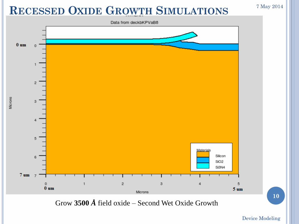
Grow 3500 Å field oxide – Second Wet Oxide Growth

RECESSED OXIDE GROWTH SIMULATIONS 7
Ma
y 2
01
4
11
Device
Mod
elin
g
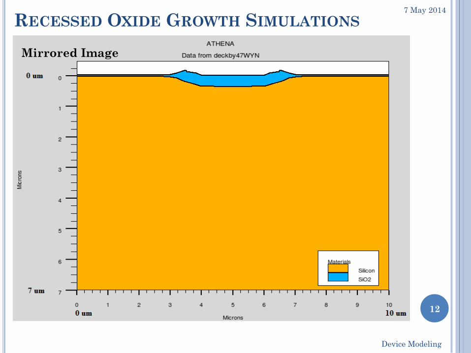
Etch all nitride.
RECESSED OXIDE GROWTH SIMULATIONS 7 May 2014
12
Device Modeling
Mirrored Image

WELL IMPLANTS-NMOS (PWELL)
7 May 2014
13
Device Modeling
Figure on the left shows the scattering of impurities in Silicon and Figure on the right shows the scattered
profile after well implant.
Impurity – Boron
Dose – 7.0e13 cm-2
Energy – 100 KeV

WELL IMPLANTS-PMOS (N WELL)
7 May 2014
14
Device Modeling
Figure on the left shows the scattering of impurities in Silicon and Figure on the right shows the scattered
profile after well implant.
Impurity – Phosphorus
Dose – 5.0e13 cm-2
Energy – 170 KeV

WELL DRIVE-IN: NMOS(PWELL) 7 May 2014
15
Device Modeling
Well Drive-In:
4 hours soak: Nitrogen Ambient
Temp: 1000˚C
Junction depth: 1.4 µm
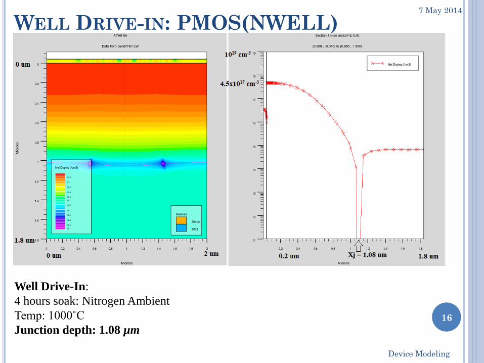
WELL DRIVE-IN: PMOS(NWELL) 7 May 2014
16
Device Modeling
Well Drive-In:
4 hours soak: Nitrogen Ambient
Temp: 1000˚C
Junction depth: 1.08 µm

RETROGRADE WELL IMPLANT 7 May 2014
Device Modeling
17
NMOS PMOS
Retrograde Well Implant
Impurity: Boron
Dose: 1.0e14 cm-2
Energy: 45 KeV
Retrograde Well Implant
Impurity: Phosphorus
Dose: 9.0e13 cm-2
Energy: 70 KeV
Retrograde profile can be noticed after a thermal anneal or after a thermal oxide growth step
Impurity =B11 Impurity = P31

GATE OXIDE GROWTH 7 May 2014
18
Device Modeling
ATHENA does not model the incorporation of nitrogen in the gate oxide growth.
So, Oxy-Nitride is deposited as a dielectric material in this model.
The thickness of the gate oxide is 30Å.

POLY-SILICON DEPOSITION 7 May 2014
19
Device Modeling
A layer of Poly-Silicon is deposited at 610ºC. Poly is 2500Å thick.
ETCH POLY-SILICON 7 May 2014
20
Device Modeling
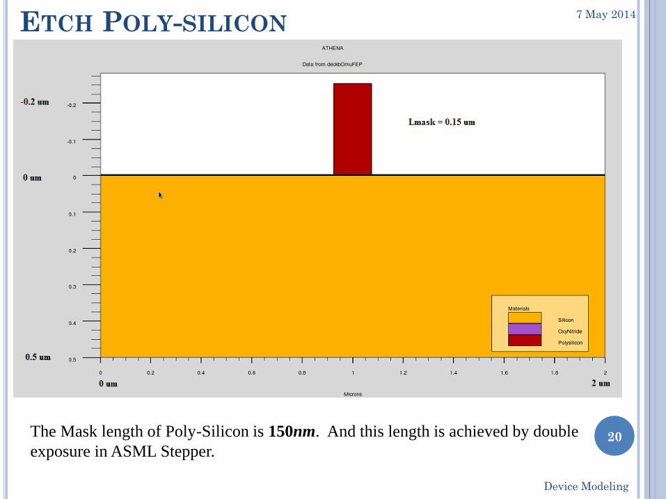
The Mask length of Poly-Silicon is 150nm. And this length is achieved by double
exposure in ASML Stepper.

POLY RE-OXIDATION AND RETROGRADE WELL PROFILE 7 May 2014
21
Device Modeling
250Å thick oxide is grown and retrograde well profile is obtained during this
oxidation step.
Concentration of impurities at the surface is comparatively greater than the
concentration of impurities at the bulk (0.2 µm deep).
The mask length of the polysilicon (150 nm) is reduced to ~125 nm after Poly-
Reoxidation.
NMOS

POLY RE-OXIDATION AND RETROGRADE WELL PROFILE 7 May 2014
22
Device Modeling
Concentration at the surface = 5e18cm-3
Concentration at the bulk = ~3e17 cm-3
PMOS

SOURCE/DRAIN EXTENSIONS IMPLANT - NMOS 7 May 2014
23
Device Modeling
Impurity : Arsenic
Dose : 5e15 cm-2
Energy: 20 KeV
Depth: 25 nm (0.025 µm)
NMOS

SOURCE/DRAIN EXTENSIONS IMPLANT - PMOS 7 May 2014
24
Device Modeling
Impurity : BF2
Dose : 9e14 cm-2
Energy: 20 KeV
Junction depth: 26 nm (0.026 µm)
PMOS
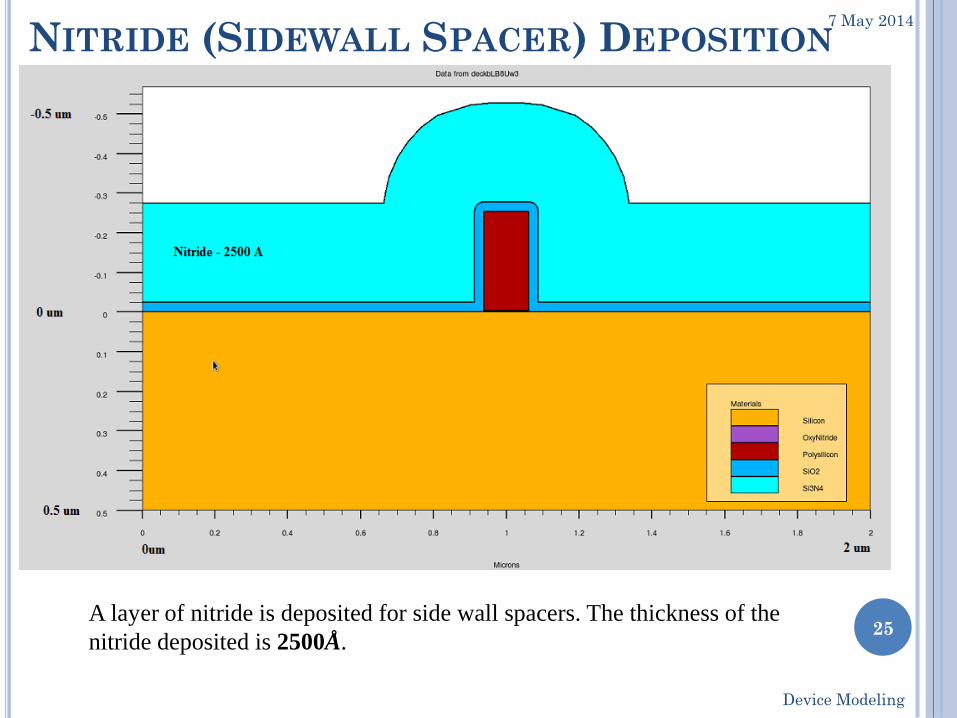
NITRIDE (SIDEWALL SPACER) DEPOSITION 7 May 2014
25
Device Modeling
A layer of nitride is deposited for side wall spacers. The thickness of the
nitride deposited is 2500Å.
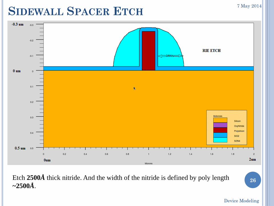
SIDEWALL SPACER ETCH 7 May 2014
26
Device Modeling
Etch 2500Å thick nitride. And the width of the nitride is defined by poly length
~2500Å.
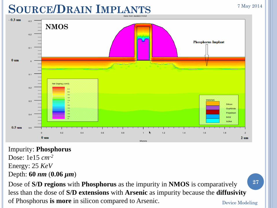
SOURCE/DRAIN IMPLANTS 7 May 2014
27
Device Modeling
Impurity: Phosphorus
Dose: 1e15 cm-2
Energy: 25 KeV
Depth: 60 nm (0.06 µm)
Dose of S/D regions with Phosphorus as the impurity in NMOS is comparatively
less than the dose of S/D extensions with Arsenic as impurity because the diffusivity
of Phosphorus is more in silicon compared to Arsenic.
NMOS
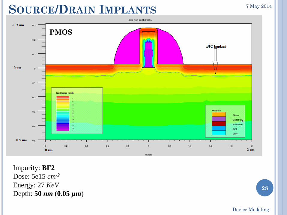
SOURCE/DRAIN IMPLANTS 7 May 2014
28
Device Modeling
Impurity: BF2
Dose: 5e15 cm-2
Energy: 27 KeV
Depth: 50 nm (0.05 µm)
PMOS

SOURCE/DRAIN SPIKE ANNEALING 7 May 2014
29
Device Modeling
NMOS
Spike Annealing is preferred over conventional furnace annealing to reduce the effects of transient enhanced
diffusion (TED).
Effects of TED is significant at low temperatures (700˚C to 950˚C).
Anneal Recipe:
Ramp up – 700˚C to 1050˚C – 3 seconds
Soak – 1050˚C – 7 seconds (Nitrogen ambient)
Ramp down - 1050˚C to 700˚C – 6 seconds
Junction depth after anneal:
NMOS (S/D regions): 105 nm ( 0.105 µm)

JUNCTION PROFILE - NMOS 7 May 2014
30
Device Modeling
Vertical cut line
Junction depth (Source/Drain Extension) = 0.05 µm
Junction depth (Source/Drain) = 0.12 µm

HORIZONTAL CUT-LINE - NMOS 7 May 2014
31
Device Modeling

SOURCE/DRAIN SPIKE ANNEALING 7 May 2014
32
Device Modeling
P+ BF2 P+ BF2
Anneal Recipe:
Ramp up – 700˚C to 1050˚C – 3 seconds
Soak – 1050˚C – 5 seconds (Nitrogen ambient)
Ramp down - 1050˚C to 700˚C – 6 seconds
Junction depth after anneal:
PMOS (S/D regions): ~100 nm ( ~0.1 µm)
PMOS

JUNCTION PROFILE - PMOS 7 May 2014
33
Device Modeling
Vertical cut line
Junction depth (Source/Drain Extension) = 0.05 µm
Junction depth (Source/Drain) = 0.09 µm

HORIZONTAL CUT-LINE - PMOS 7 May 2014
34
Device Modeling

TITANIUM DEPOSITION 7 May 2014
35
Device Modeling
Etch oxide and sputter 300Ǻ thick Titanium to form Silicide.

SILICIDE (TISI) 7 May 2014
Device Modeling
36
NMOS PMOS
Silicide recipe:
Ramp up – 25˚C to 650˚C – 5 seconds
Soak – 650˚C – 5 seconds (Nitrogen ambient)
Ramp down – 650˚C to 25˚C – 5 seconds

ETCH TITANIUM AND SILICIDE (TISI2) 7 May 2014
Device Modeling
37
NMOS PMOS
Silicide recipe:
Ramp up – 25˚C to 700˚C – 5 seconds
Soak – 700˚C – 5 seconds (Nitrogen ambient)
Ramp down – 700˚C to 25˚C – 10 seconds

TEOS DEPOSITION 7 May 2014
Device Modeling
38
NMOS PMOS
Deposit 3000Ǻ thick TEOS on P5000.

CONTACT CUT ETCH (RIE) 7 May 2014
Device Modeling
39
NMOS PMOS

ALUMINUM DEPOSITION 7 May 2014
40
Device Modeling
Sputter 4000Ǻ thick Aluminum.

ALUMINUM ETCH 7 May 2014
Device Modeling
41
NMOS PMOS

FINAL NMOS DEVICE 7 May 2014
42
Device Modeling

FINAL PMOS DEVICE 7 May 2014
43
Device Modeling

I-V CURVES (THRESHOLD VOLTAGE CURVES) 7 May 2014
Device Modeling
44
NMOS PMOS
NMOS:
Threshold voltage: 0.4794V
PMOS:
Threshold voltage: -0.58V
Models cvt srh print
Contact name=gate n.poly (NMOS) / p.poly (PMOS)
Interface qf=3e11

DRAIN INDUCED BARRIER LOWERING CURVES 7 May 2014
Device Modeling
45
NMOS PMOS
DIBL: 10.3 mV/V
Current at 0V ~ 10-12 A/µm
Sub-threshold Slope: 108 mV/decade
DIBL: 11.7 mV/V
Current at 0V ~ 10-14 A/µm
Sub-threshold Slope: 96 mV/decade
Models cvt srh print
Contact name=gate n.poly (NMOS) / p.poly (PMOS)
Interface qf=3e11
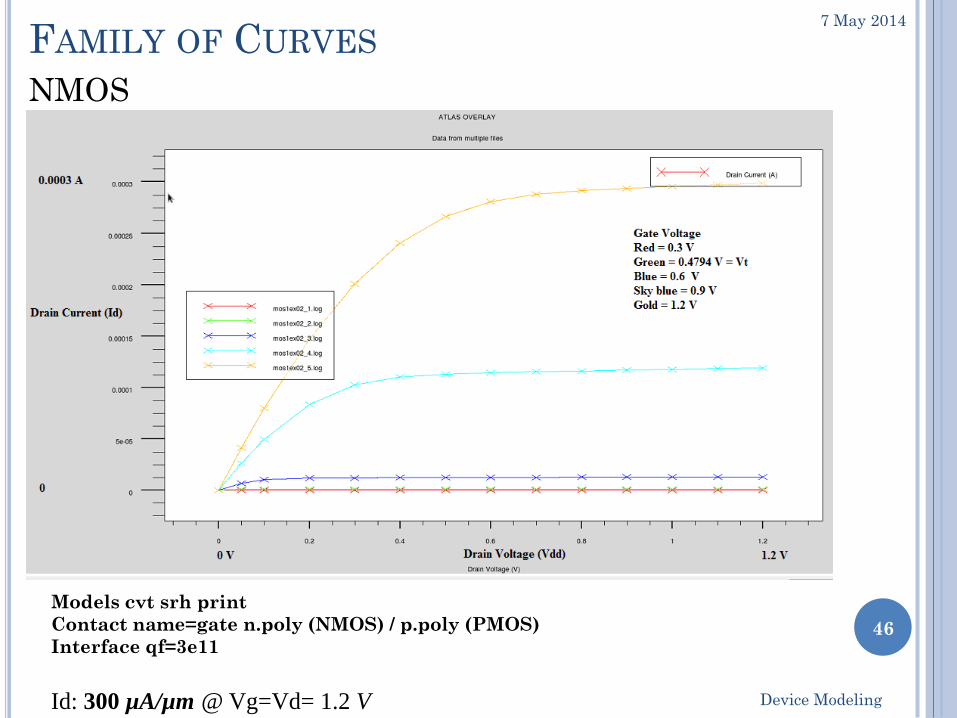
FAMILY OF CURVES
NMOS
7 May 2014
46
Device Modeling
Models cvt srh print
Contact name=gate n.poly (NMOS) / p.poly (PMOS)
Interface qf=3e11
Id: 300 µA/µm @ Vg=Vd= 1.2 V
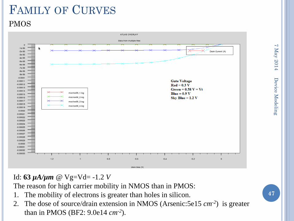
FAMILY OF CURVES 7
Ma
y 2
01
4
47
Device
Mod
elin
g
PMOS
Id: 63 µA/µm @ Vg=Vd= -1.2 V
The reason for high carrier mobility in NMOS than in PMOS:
1. The mobility of electrons is greater than holes in silicon.
2. The dose of source/drain extension in NMOS (Arsenic:5e15 cm-2) is greater
than in PMOS (BF2: 9.0e14 cm-2).

CHANGES REQUIRED
Changes to be made in the existing process and in MESA are
Well implant dose and energy.
Reduction in anneal time from 5 hours to 4 hours (Thermal Budget).
Retrograde well implant
Removal of threshold adjust implants.
Develop a recipe to deposit a thin layer of gate oxide.
Develop recipes to deposit thin layer of Titanium.
Develop Source/drain anneal recipe on RTP tool for spike annealing.
7 May 2014
48
Device Modeling
REFERENCES
Bruce furnace recipes
http://people.rit.edu/lffeee/Bruce_Furnace.pdf
Diffusion and implant models, ‘Athena user
manual’
Electrical simulation models, ‘Atlas user manual’
7 May 2014
49
Device Modeling