Embed Size (px)
Citation preview
Modal study of GaAs waveguides with zinc-diffused
boundaries
S. Iraj Najafi, Chunmeng Wu, John F. Currie and Tahar Touam
Single-mode planar channel waveguides are produced by zinc diffusion in GaAs. A Zn-doped spin-on-glass
(glass forming solution) is used as the diffusion source. The modal behavior of the fabricated waveguides is
experimentally investigated. A simple model is'used to analyze these waveguides.
Ridge waveguides have been the most popular struc-ture to fabricate passive and active integrated opticscomponents in GaAs. Propagation losses of -0.2 dB/cm have been achieved.1 However, ridge structure canproduce electrical interconnection problems when sev-eral components have to be made on the same sub-strate. Planar2 waveguides are attractive alternativesto avoid this problem. There have been a few at-tempts to manufacture planar waveguide devices inGaAs. Somekh et al.3 employed proton implantation.They fabricated waveguides with propagation losses of26.1 dB/cm. Be+ bombardment in GaAs was utilizedby Leonberger et al.4 They demonstrated 4.3-dB/cmpropagation losses. Swanson et al.5 used sealed-am-pule Zn diffusion to fabricate GaAs waveguides withpropagation losses of 8.7 dB/cm. We recently report-ed6 fabrication of channel waveguides in GaAs withzinc-diffused boundaries using a spin-on-glass (SOG)diffusion source.7 In this paper we report on an ex-perimental and theoretical study of the modal behav-ior of these components.
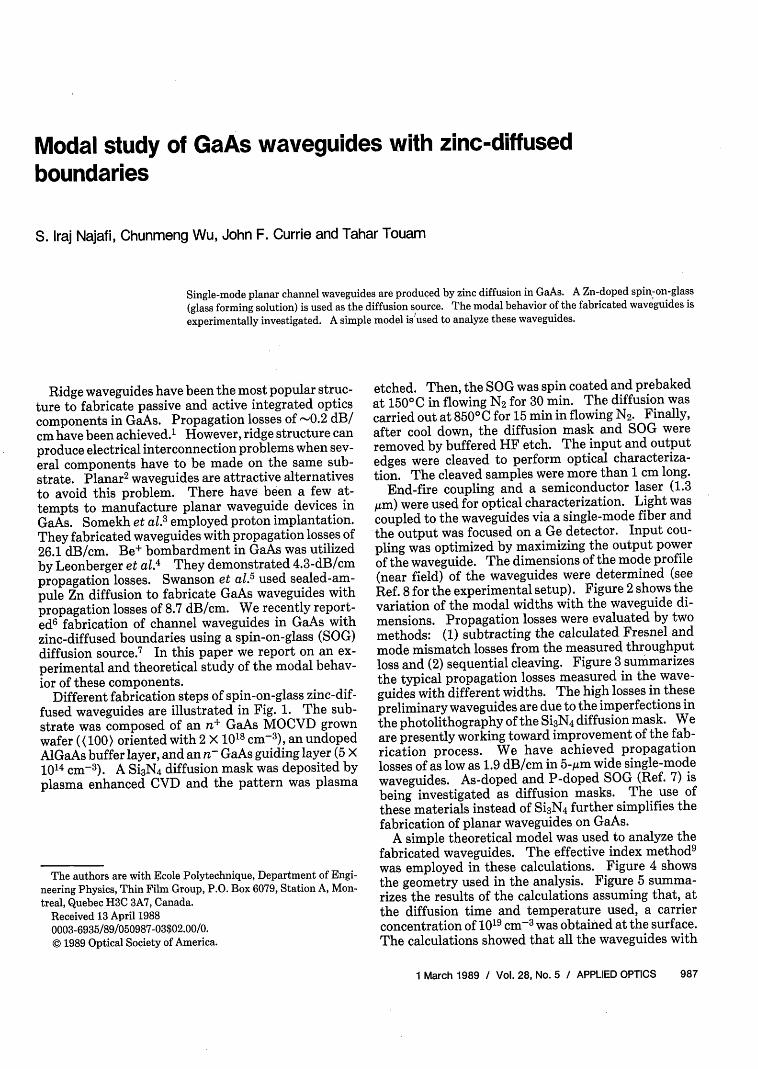
Different fabrication steps of spin-on-glass zinc-dif-fused waveguides are illustrated in Fig. 1. The sub-strate was composed of an n+ GaAs MOCVD grownwafer ((100) oriented with 2 X 1018 cm-3 ), an undopedAlGaAs buffer layer, and an n- GaAs guiding layer (5 X1014 cm- 3 ). A Si3 N4 diffusion mask was deposited byplasma enhanced CVD and the pattern was plasma
The authors are with Ecole Polytechnique, Department of Engi-
neering Physics, Thin Film Group, P.O. Box 6079, Station A, Mon-
treal, Quebec H3C 3A7, Canada.Received 13 April 1988
0003-6935/89/050987-03$02.00/0.© 1989 Optical Society of America.
etched. Then, the SOG was spin coated and prebakedat 1500C in flowing N2 for 30 min. The diffusion wascarried out at 8500C for 15 min inflowing N2. Finally,after cool down, the diffusion mask and SOG wereremoved by buffered HF etch. The input and outputedges were cleaved to perform optical characteriza-tion. The cleaved samples were more than 1 cm long.
End-fire coupling and a semiconductor laser (1.3Aum) were used for optical characterization. Light wascoupled to the waveguides via a single-mode fiber andthe output was focused on a Ge detector. Input cou-pling was optimized by maximizing the output powerof the waveguide. The dimensions of the mode profile(near field) of the waveguides were determined (seeRef. 8 for the experimental setup). Figure 2 shows thevariation of the modal widths with the waveguide di-mensions. Propagation losses were evaluated by twomethods: (1) subtracting the calculated Fresnel andmode mismatch losses from the measured throughputloss and (2) sequential cleaving. Figure 3 summarizesthe typical propagation losses measured in the wave-guides with different widths. The high losses in thesepreliminary waveguides are due to the imperfections inthe photolithography of the Si3N4 diffusion mask. Weare presently working toward improvement of the fab-rication process. We have achieved propagationlosses of as low as 1.9 dB/cm in 5-,um wide single-modewaveguides. As-doped and P-doped SOG (Ref. 7) isbeing investigated as diffusion masks. The use ofthese materials instead of Si3N4 further simplifies thefabrication of planar waveguides on GaAs.
A simple theoretical model was used to analyze thefabricated waveguides. The effective index method9
was employed in these calculations. Figure 4 showsthe geometry used in the analysis. Figure 5 summa-rizes the results of the calculations assuming that, atthe diffusion time and temperature used, a carrierconcentration of 1019 cm-3 was obtained at the surface.The calculations showed that all the waveguides with
1 March 1989 / Vol. 28, No. 5 / APPLIED OPTICS 987

n 2
t
-Zn-SOG
4.5pmIlPm
Fig. 1. Different
E
00
0i00.
t
Si3 N4n, I|-n-GaAsn2 ~ Al0 4 Ga.96As
- n- n'GaAs
steps of spin-on-glass zinc-diffused GaAs wave-guide fabrication.
10
9
8
7
6
5
4
3
2
1.1 1.5 2.0 2.5 3.0 3.5 4.0 4.5 5.0 5.5
W(P m)
Fig. 3. Variation of propagation losses with waveguide width in thewaveguides with a Si3N 4 diffusion mask: *, propagation lossesequals throughput loss minus Fresnel and mode mismatch losses; +,sequential cleaving. The length of the original sample was 13 mm.
1.5 2.0 2.5 3.0 3.5 4.0 4.5 5.0 5.5
:- W -II I I
n 4
n3
n 2
n,
. n4
n3
ni
- Zn-diffused_- r_-GaAs
A , 4 Ga.,,As
-n+Ga As
n
ni
Ln2
Fig. 4. Model used for analysis of zinc-diffused waveguides.
W(IJm)
Fig. 2. Variation of lateral and transverse mode width (at leheight) with waveguide width. Diffusion time was 15 min. Inset is
the mode profile (near field) of a 5-,um wide waveguide.
-4.5-Mm diffusion depth and <5-,um width were singlemode. This was verified experimentally: (1) opticalmeasurements revealed that all the waveguides with1.5-5-,m width were single mode and (2) stain etchingshowed that zinc was diffused 4-4.5 ,um in the guidinglayer.
In summary, we have fabricated, characterized, andanalyzed zinc-diffused channel waveguides using aspin-on-glass diffusion source. This technique is sig-nificantly simpler than the previously reported meth-ods3 -5 for the fabrication of planar waveguides onGaAs and relatively low-loss waveguides can be made.However, the propagation losses in our waveguides arestill higher than the ridge waveguides and the modesare asymmetrical, because the substrate was designed
z
,48Y --- d=3.0 PuM
-- d=4. PM
448 =T Ea
147 ,// / E_- /-_
./ ./
0 5 10 15
W(PIm)
Fig. 5. Calculated variation of the effective index, Nff, with wave-guide width W in zinc-diffused waveguides for different values of
diffusion depth d.
988 APPLIED OPTICS / Vol. 28, No. 5 / 1 March 1989
L + +* +. S +
. * ~* .+ -
. ~~~~~~~+
A T=1.3PM
TE
21
19
171
151
13
1t1l
9
7
5 I_1.0
0
0
E
I0
0
C0
'0
-j
I I
+ . 0 + +
* 0 0 .0
u.zaH"'I |l
n twIsmt_
o
3.i
3.d
- I

for ridge waveguide fabrication. 1 0 The excess lossesare due to the interaction of the evanescent field withthe Zn-diffused boundaries. The guiding layer intro-duces only -0.1 dB/cm of loss.10 Therefore, the prop-agation losses can be reduced considerably by modify-ing the substrate design and fabrication parameters.Our preliminary calculations indicate that losses below1 dB/cm can be achieved. Another layer of AlGaAscan be used as a cover to reduce losses and makesymmetrical mode profiles.
This work was supported in part by a research grantfrom Alcan International LTD (Kingston Laborato-ries, Canada).References
1. For example, H. Inoue, K. Hiruma, K. Ishida, T. Asai, and H.
Matsumura, "Low Loss GaAs Optical Waveguides," IEEE/OSAJ. Lightwave Technol. LT-3, 1270 (1985).
2. We distinguish between slab and planar waveguides. In a slab
waveguide light is confined in one dimension. We use the termplanar in contrast with ridge, rib, or buried. Therefore, a planarwaveguide can be a channel or a slab waveguide. In this paper,
we discuss planar channel waveguides.
3. S. Somekh, E. Garmire, A. Yariv, H. L. Garvin, and R. G. Hun-sperger, "Channel Optical Waveguides and Directional Cou-plers in GaAs-Imbedded and Ridged," Appl. Opt. 13, 327
(1974).4. F. J. Leonberger, J. P. Donnelly, and C. 0. Bozler, "GaAs
P+n-n+ Directional Coupler Switch," Appl. Phys. Lett. 29, 652(1976).
5. P. D. Swanson, F. Julien, M. A. Emanuel, L. Sloan, T. Tang, T. A.DeTemple, and J. J. Coleman, "Low-Loss SemiconductorWaveguide Bends," Opt. Lett. 13, 245 (1988).
6. T. Touam, C. Wu, M. Belanger, and S. I. Najafi, "GaAs Zn-Diffused Waveguides," presented at CAP/APS Joint Congress,Montreal (June 1988), paper FF6.
7. Available, for example, from Emulsiton Co., 19 Leslie Court,Whippany, NJ.
8. S. I. Najafi, "Optical Behavior of Potassium Ion-ExchangedGlass Waveguides," Appl. Opt. 27, 3728 (1988).
9. G. B. Hocker and W. K. Burns, "Mode Dispersion in DiffusedChannel Waveguides by the Effective Index Method," Appl.Opt. 16, 113 (1977).
10. M. Belanger, S. I. Najafi, J. F. Currie, and R. Maciejko, "Fabrica-tion and Characterization of a Linear Mode Confinement Mod-ulator on GaAs," IEEE J. Selected Areas in Communications(Joint issue with IEEE/OSA J. Lightwave Tech.) 6,1205 (1988).
OPTCON1988
Joseph H. Good, Jr.NASA Langley
James J. BurkeU. Arizona
photos:F. S. Harris, Jr.
Paul F. LiaoBellcore
1 March 1989 / Vol. 28, No. 5 / APPLIED OPTICS 989