Embed Size (px)
Citation preview

Mobile Intel® Pentium® III Processor-M Datasheet
October 2001
Order Number: 298340-002
R
Mobile Intel® Pentium® III Processor-M Datasheet
2 Datasheet 298340-002
Information in this document is provided in connection with Intel products. No license, express or implied, by estoppel or otherwise, to any intellectual property rights is granted by this document. Except as provided in Intel’s Terms and Conditions of Sale for such products, Intel assumes no liability whatsoever, and Intel disclaims any express or implied warranty, relating to sale and/or use of Intel products including liability or warranties relating to fitness for a particular purpose, merchantability, or infringement of any patent, copyright or other intellectual property right. Intel products are not intended for use in medical, life saving, or life sustaining applications. Intel may make changes to specifications and product descriptions at any time, without notice. Designers must not rely on the absence or characteristics of any features or instructions marked "reserved" or "undefined." Intel reserves these for future definition and shall have no responsibility whatsoever for conflicts or incompatibilities arising from future changes to them. The Mobile Intel® Pentium® III Processor-M may contain design defects or errors known as errata which may cause the product to deviate from published specifications. Current characterized errata are available on request. Contact your local Intel sales office or your distributor to obtain the latest specifications and before placing your product order. Copies of documents which have an ordering number and are referenced in this document, or other Intel literature, may be obtained from: Intel Corporation www.intel.com or call 1-800-548-4725 Intel®, Pentium®, and SpeedStepTM are registered trademarks or trademarks of Intel Corporation in the United States and other countries. *Other names and brands may be claimed as the property of others. Copyright © Intel Corporation 2000-2001
Mobile Intel® Pentium ® III Processor-M Datasheet
298340-002 Datasheet 3
Contents
1. Introduction.....................................................................................................................................10 1.1 Overview...............................................................................................................11 1.2 State of the Data ..................................................................................................11 1.3 Terminology..........................................................................................................12 1.4 References ...........................................................................................................12
2. Mobile Intel Pentium III Processor-M Features ..............................................................................13 2.1 New Features in the Mobile Pentium III Processor-M..........................................13
2.1.1 133-MHz PSB With AGTL Signaling .......................................................13 2.1.2 512K On-die Integrated L2 Cache ..........................................................13 2.1.3 Data Prefetch Logic.................................................................................13 2.1.4 Differential Clocking ................................................................................13 2.1.5 Deeper Sleep State .................................................................................13 2.1.6 Signal Differences Between the Mobile Pentium III Processor (in BGA2 and Micro-PGA2 Packages) and the Mobile Intel Pentium III Processor-M ............................................................................................14
2.2 Power Management .............................................................................................14 2.2.1 Clock Control Architecture.......................................................................14 2.2.2 Normal State ...........................................................................................14 2.2.3 Auto Halt State ........................................................................................14 2.2.4 Quick Start State .....................................................................................15 2.2.5 HALT/Grant Snoop State ........................................................................16 2.2.6 Deep Sleep State ....................................................................................16 2.2.7 Deeper Sleep State .................................................................................16 2.2.8 Operating System Implications of Low-power States .............................17 2.2.9 Enhanced Intel SpeedStep Technology..................................................17
2.3 AGTL Signals .......................................................................................................17 2.4 Mobile Intel Pentium III Processor-M CPUID .......................................................18
3. Electrical Specifications..................................................................................................................19 3.1 Processor System Signals ...................................................................................19
3.1.1 Power Sequencing Requirements...........................................................20 3.1.2 Test Access Port (TAP) Connection .......................................................21 3.1.3 Catastrophic Thermal Protection.............................................................21 3.1.4 Unused Signals .......................................................................................21 3.1.5 Signal State in Low-power States ...........................................................21
3.2 Power Supply Requirements................................................................................22 3.2.1 Decoupling Guidelines ............................................................................22 3.2.2 Voltage Planes ........................................................................................23 3.2.3 Voltage Identification ...............................................................................23
3.3 System Bus Clock and Processor Clocking .........................................................24 3.4 Enhanced Intel SpeedStep Technology...............................................................24 3.5 Maximum Ratings.................................................................................................25 3.6 DC Specifications .................................................................................................25

Mobile Intel® Pentium® III Processor-M Datasheet
4 Datasheet 298340-002
3.7 AC Specifications................................................................................................. 35 3.7.1 System Bus, Clock, APIC, TAP, CMOS, and Open-drain AC Specifications.......................................................................................... 35
4. System Signal Simulations ............................................................................................................ 50 4.1 System Bus Clock (BCLK) and PICCLK DC Specifications and AC Signal Quality
Specifications....................................................................................................... 50 4.2 AGTL AC Signal Quality Specifications ............................................................... 52 4.3 Non-AGTL Signal Quality Specifications ............................................................. 54
4.3.1 PWRGOOD, VTTPWRGD Signal Quality Specifications ....................... 54 5. Mechanical Specifications.............................................................................................................. 55
5.1 Socketable Micro-FCPGA Package..................................................................... 55 5.2 Surface Mount Micro-FCBGA Package............................................................... 59 5.3 Signal Listings...................................................................................................... 63
6. VCC Thermal Specifications............................................................................................................ 70 6.1 Thermal Diode ..................................................................................................... 71
7. Processor Initialization and Configuration ..................................................................................... 73 7.1 Description ........................................................................................................... 73
7.1.1 Quick Start Enable .................................................................................. 73 7.1.2 System Bus Frequency........................................................................... 73 7.1.3 APIC Enable ........................................................................................... 73
7.2 Clock Frequencies and Ratios............................................................................. 73 8. Processor Interface........................................................................................................................ 75
8.1 Alphabetical Signal Reference............................................................................. 75 8.2 Signal Summaries................................................................................................ 85
Appendix A. PLL RLC Filter Specification .................................................................................................. 87 A1. Introduction ......................................................................................................... 87 A2. Filter Specification............................................................................................... 87 A3. Recommendation for Mobile Systems................................................................ 88 A4. Comments........................................................................................................... 89

Mobile Intel® Pentium ® III Processor-M Datasheet
298340-002 Datasheet 5
Figures Figure 1. Clock Control States ..........................................................................................15 Figure 2. PLL RLC Filter....................................................................................................23 Figure 3. VTTPWRGD System-Level Connections...........................................................24 Figure 4. Illustration of VCC Static and Transient Tolerances (VID = 1.40V)....................29 Figure 5. Illustration of Deep Sleep VCC Static and Transient Tolerances (VID setting = 1.40V) .............................................................................................................30 Figure 6. BCLK (Single Ended)/PICCLK/TCK Generic Clock Timing Waveform .............41 Figure 7. Differential BCLK/BCLK# Waveform (Common Mode) .....................................41 Figure 8. BCLK/BCLK# Waveform (Differential Mode) .....................................................42 Figure 9. Valid Delay Timings ...........................................................................................42 Figure 10. Setup and Hold Timings...................................................................................43 Figure 11. Cold/Warm Reset and Configuration Timings..................................................43 Figure 12. Power-on Sequence and Reset Timings ..........................................................44 Figure 13. Power Down Sequencing and Timings (VCC Leading) ...................................45 Figure 14. Power Down Sequencing and Timings (VCCT Leading) ....................................46 Figure 15. Test Timings (Boundary Scan) .........................................................................47 Figure 16. Test Reset Timings ...........................................................................................47 Figure 17. Quick Start/Deep Sleep Timing (BCLK Stopping Method) ...............................48 Figure 18. Quick Start/Deep Sleep Timing (DPSLP# Assertion Method) ..........................48 Figure 19. Enhanced Intel SpeedStep Technology/Deep Sleep Timing...........................49 Figure 20. BCLK (Single Ended)/PICCLK Generic Clock Waveform ................................51 Figure 21. Maximum Acceptable Overshoot/Undershoot Waveform.................................52 Figure 22. Socketable Micro-FCPGA Package - Top and Bottom Isometric Views ..........56 Figure 23. Socketable Micro-FCPGA Package - Top and Side View ................................57 Figure 24. Socketable Micro-FCPGA Package - Bottom View .........................................58 Figure 25. Micro-FCBGA Package – Top and Bottom Isometric Views ............................60 Figure 26. Micro-FCBGA Package – Top and Side Views ................................................61 Figure 27. Micro-FCBGA Package - Bottom View .............................................................62 Figure 28. Pin/Ball Map - Top View...................................................................................63 Figure 29. PLL Filter Specifications ..................................................................................88

Mobile Intel® Pentium® III Processor-M Datasheet
6 Datasheet 298340-002
Tables Table 1. New and Revised Mobile Intel Pentium III Processor-M Signals ....................... 14 Table 2. Clock State Characteristics................................................................................. 17 Table 3. Mobile Pentium III Processor-M CPUID ............................................................. 18 Table 4. Mobile Pentium III Processor-M CPUID Cache and TLB Descriptors................ 18 Table 5. System Signal Groups ........................................................................................ 19 Table 6. Recommended Resistors for Mobile Intel Pentium III Processor-M Signals ...... 20 Table 7. Mobile Intel Pentium III Processor-M VID Values............................................... 23 Table 8. Mobile Intel Pentium III Processor-M Absolute Maximum Ratings..................... 25 Table 9. Power Specifications for Mobile Intel Pentium III Processor-M .......................... 26 Table 10. VCC Tolerances for the Mobile Intel Pentium III Processor-M : VID = 1.40V
(Performance Mode) and 1.15V (Battery Optimized Mode)............................. 28 Table 11. VCC Tolerances for the Mobile Intel Pentium III Processor-M in the Deep Sleep
State : VID = 1.40V (Performance Mode) and 1.15V (Battery Optimized Mode) ................................................................................................................ 30 Table 12. VCC Tolerances for the Low Voltage Mobile Intel Pentium III Processor-M: VID = 1.15V (Performance Mode) and 1.05V (Battery Optimized Mode) ......... 31 Table 13. VCC Tolerances for the Low Voltage Mobile Intel Pentium III Processor-M in the
Deep Sleep State: VID = 1.15V (Performance Mode) and 1.05V (Battery Optimized Mode) ............................................................................................... 31 Table 14. VCC Tolerances for the Ultra Low Voltage Mobile Intel Pentium III Processor-M: VID = 1.1V (Performance Mode) and 0.95V (Battery Optimized Mode) ................................................................................................................ 32 Table 15. VCC Tolerances for the Ultra Low Voltage Mobile Intel Pentium III Processor-M in
the Deep Sleep State: VID = 1.1V (Performance Mode) and 0.95V (Battery Optimized Mode) .............................................................................................. 32
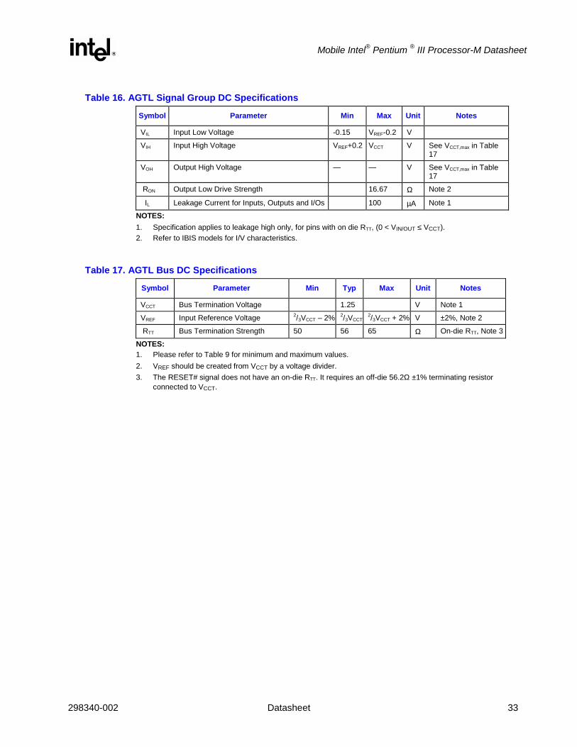
Table 16. AGTL Signal Group DC Specifications............................................................. 33 Table 17. AGTL Bus DC Specifications............................................................................ 33 Table 18. CLKREF, APIC, TAP, CMOS, and Open-drain Signal Group DC Specifications .................................................................................................... 34 Table 19. System Bus Clock AC Specifications (Differential) ......................................... 35 Table 20. System Bus Clock AC Specifications (133 MHz, Single Ended)...................... 36 Table 21. System Bus Clock AC Specifications (100 MHz, Single Ended)...................... 36 Table 22. Valid Mobile Intel Pentium III Processor-M Frequencies.................................. 37 Table 23. AGTL Signal Groups AC Specifications ........................................................... 38 Table 24. CMOS and Open-drain Signal Groups AC Specifications..................................................38 Table 25. Reset Configuration AC Specifications and Power On/Power Down Timings . 39 Table 26. APIC Bus Signal AC Specifications .................................................................. 39 Table 27. TAP Signal AC Specifications........................................................................... 40 Table 28. Quick Start/Deep Sleep AC Specifications....................................................... 40 Table 29. Enhanced Intel SpeedStep Technology AC Specifications.............................. 41 Table 30. BCLK (Differential) DC Specifications and AC Signal Quality Specifications .. 50 Table 31. BCLK (Single Ended) DC Specifications and AC Signal Quality Specifications .................................................................................................... 50 Table 32. PICCLK DC Specifications and AC Signal Quality Specifications.................... 51 Table 33. 133-MHz AGTL Signal Group Overshoot/Undershoot Tolerance at the Processor Core ................................................................................................. 53 Table 34. 100-MHz AGTL Signal Group Overshoot/Undershoot Tolerance at the Processor Core ................................................................................................. 53 Table 35. Non-AGTL Signal Group Overshoot/Undershoot Tolerance at the Processor Core................................................................................................................... 54 Table 36. Socketable Micro-FCPGA Package Specification ............................................ 55

Mobile Intel® Pentium ® III Processor-M Datasheet
298340-002 Datasheet 7
Table 37. Micro-FCBGA Package Mechanical Specifications ..........................................59 Table 38. Signal Listing in Order by Pin/Ball Number.......................................................64 Table 39. Signal Listing in Order by Signal Name ............................................................67 Table 40. Voltage and No-Connect Pin/Ball Locations .....................................................69 Table 41. Power Specifications for Mobile Intel Pentium III Processor-M.........................70 Table 42. Thermal Diode Interface....................................................................................71 Table 43. Thermal Diode Specifications ...........................................................................72 Table 44. BSEL[1:0] Encoding ..........................................................................................78 Table 45. Input Signals......................................................................................................85 Table 46. Output Signals...................................................................................................85 Table 47. Input/Output Signals (Single Driver)..................................................................86 Table 48. Input/Output Signals (Multiple Driver) ...............................................................86 Table 49. PLL Filter Inductor Recommendations..............................................................88 Table 50. PLL Filter Capacitor Recommendations ...........................................................88 Table 51. PLL Filter Resistor Recommendations..............................................................89

Mobile Intel® Pentium® III Processor-M Datasheet
8 Datasheet 298340-002
Revision History
Revision Description Date 001 Initial release July 2001
002 Revision 2.0 Updates include:
• Added new mobile Intel® Pentium® III Processor-M 1.2 GHz • Added new Low Voltage mobile Intel Processor-M 800/533, 800A/500,
750/450, 733/466 MHz speeds • Added new Ultra Low Voltage mobile Intel Processor-M 700/300 MHz
speed • Updated Processor Specifications (Tables 9, 12-15, 42)
• Load lines updated • Updated Section 5 and tables 36, 37 with additional package details
• Updated references
October 2001

Mobile Intel® Pentium ® III Processor-M Datasheet
298340-002 Datasheet 9
Mobile Intel® Pentium® Processor-M Product Features ! Supports Enhanced Intel® SpeedStepTM
technology with the following Processor core/bus speeds: 1200/133 MHz (Maximum Performance
Mode) and 800/133 MHz (Battery Optimized Mode)
1133/133 MHz (Maximum Performance Mode) and 733/133 MHz (Battery Optimized Mode)
1066/133 MHz (Maximum Performance Mode) and 733/133 MHz (Battery Optimized Mode)
1000/133 MHz (Maximum Performance Mode) and 733/133 MHz (Battery Optimized Mode)
933/133 MHz (Maximum Performance Mode) and 733/133 MHz (Battery Optimized Mode)
866/133 MHz (Maximum Performance Mode) and 667/133 MHz (Battery Optimized Mode)
! Low Voltage processors supports Enhanced Intel SpeedStep technology with the following Processor core/bus speeds: 800/133 MHz (Maximum Performance
Mode) and 533/133 MHz (Battery Optimized Mode)
733/133 MHz (Maximum Performance Mode) and 466/133 MHz (Battery Optimized Mode)
800A/100 MHz (Maximum Performance Mode) and 500/100 MHz (Battery Optimized Mode)
750/100 MHz (Maximum Performance Mode) and 450/100 MHz (Battery Optimized Mode)
! Ultra Low Voltage processor supports Enhanced Intel® SpeedStepTM technology with the following Processor core/bus speeds: 700/100 MHz (Maximum
Performance Mode) and 300/100 MHz (Battery Optimized Mode)
Feature Highlights
! Supports the Intel Architecture with Dynamic Execution
! On-die primary 16-Kbyte instruction cacheand 16-Kbyte write-back data cache
! On-die second level cache (512-Kbyte) with Advanced Transfer Cache Architecture
! Data Prefetch Logic ! Integrated AGTL termination ! Integrated math co-processor ! Micro-FCPGA and Micro-FCBGA
packaging technologies Supports thin form factor notebook
designs Exposed die enables more efficient
heat dissipation ! Fully compatible with previous Intel
microprocessors Binary compatible with all
applications Support for MMX™ technology Support for Streaming SIMD
Extensions ! Power Management Features
Quick Start, Deep Sleep and Deeper Sleep modes provide low power dissipation
! On-die thermal diode
Mobile Intel® Pentium® III Processor-M Datasheet
10 Datasheet 298340-002
1. Introduction Using Intel’s advanced 0.13-micron process technology with copper interconnect, the Mobile Intel® Pentium® III Processor-M offers high-performance and low-power consumption. The Mobile Intel Pentium III Processor-M (hereafter referred to as “the processor”) is based on the same core as existing mobile Intel® Pentium® III processors. Key performance features include Internet Streaming SIMD instructions, an Advanced Transfer Cache architecture, and a processor system bus speed of 133 MHz. These features are offered in Micro-FCPGA packages for socketable boards and Micro-FCBGA packages for surface mount boards.
The Low Voltage Mobile Intel Pentium III Processor-M will support both a 133-MHz and 100-MHz bus speed. The Ultra Low Voltage Mobile Intel Pentium III Processor-M supports a 100-MHz bus speed. The Low Voltage and Ultra Low Voltage Mobile processors will be available only in the Micro-FCBGA package. All of these technologies make outstanding performance possible for mobile PCs in a variety of shapes and sizes.
The processor, when used in conjunction with the Intel SpeedStep™ technology applet version 2.1 or its equivalent, supports Enhanced Intel SpeedStep technology, which enables real-time dynamic switching of the voltage and frequency between two performance modes based on CPU demand. This occurs by switching the bus ratios, core operating voltage, and core processor speeds without resetting the system. The processor also features a new ultra low power state called Deeper Sleep.
The 512-kB integrated L2 cache based on the Advanced Transfer Cache architecture runs at full speed and is designed to help improve performance. It complements the system bus by providing critical data faster and reducing total system power consumption. The processor also features Data Prefetch Logic that speculatively fetches data to the L2 cache, resulting in improved performance. The Mobile Pentium III Processor-M’s 64-bit wide Assisted Gunning Transceiver Logic (AGTL) system bus provides a glue-less, point-to-point interface for a memory controller hub.
This document covers the electrical, mechanical, and thermal specifications for the following:
• The Mobile Pentium III Processor-M is offered at the following frequencies and voltages (Maximum Performance mode/Battery Optimized mode): 1200/800 MHz, 1133/733 MHz, 1066/733 MHz, 1000/733 MHz, 933/733 MHz and 866/667 MHz at 1.40V/1.15V.
• The Low Voltage Mobile Intel Pentium III Processor-M is offered at the following frequencies and voltages (Maximum Performance mode/Battery Optimized mode): 800/533 MHz, 800A/500 MHz, 750/450 MHz and 733/466 MHz at 1.15V/1.05V.
• The Ultra Low Voltage Mobile Pentium III Processor-M is offered at the following frequencies and voltages (Maximum Performance mode/Battery Optimized mode): 700/300 MHz at 1.1V/0.95V.
Unless explicitly stated, all references to the Mobile Pentium III Processor-M in this document also apply to the Low Voltage and Ultra Low Voltage Mobile Pentium III Processor-M.
Mobile Intel® Pentium ® III Processor-M Datasheet
298340-002 Datasheet 11
1.1 Overview • Performance features
— Supports the Intel Architecture with Dynamic Execution — Supports the Intel Architecture MMX™ technology — Supports Streaming SIMD Extensions for enhanced video, sound, and 3D performance — Supports Enhanced Intel SpeedStep™ Technology — Integrated Intel Floating Point Unit compatible with the IEEE 754 standard — Data Prefetch Logic
• On-die primary (L1) instruction and data caches — 4-way set associative, 32-byte line size, 1 line per sector — 16-Kbyte instruction cache and 16-Kbyte write-back data cache — Cacheable range controlled by processor programmable registers
• On-die second level (L2) cache — 8-way set associative, 32-byte line size, 1 line per sector — Operates at full core speed — 512-Kbyte ECC protected cache data array
• AGTL system bus interface — 64-bit data bus, 100-MHz and 133-MHz operation — Uniprocessor, two loads only (processor and chipset) — Integrated termination
• Processor clock control — Quick Start for low power, low exit latency clock “throttling” — Deep Sleep mode for lower power dissipation — Deeper Sleep mode for lowest power dissipation
• Thermal diode for measuring processor temperature
1.2 State of the Data All information in this document is the best available information at the time of publication. Revisions of this document will be provided on an as-required basis in the Mobile Intel® Pentium® III Processor and Mobile Intel® Pentium® III Processor-M Specification Update.
Mobile Intel® Pentium® III Processor-M Datasheet
12 Datasheet 298340-002
1.3 Terminology Term Definition
# A “#” symbol following a signal name indicates that the signal is active low. This means that when the signal is asserted (based on the name of the signal) it is in an electrical low state. Otherwise, signals are driven in an electrical high state when they are asserted. In state machine diagrams, a signal name in a condition indicates the condition of that signal being asserted
! Indicates the condition of that signal not being asserted. For example, the condition “!STPCLK# and HS” is equivalent to “the active low signal STPCLK# is unasserted (i.e., it is at 1.5V) and the HS condition is true.”
L Electrical low signal levels H Electrical high signal levels 0 Logical low. For example, BD[3:0] = “1010” = “HLHL” refers to a hexadecimal “A,” and D[3:0]# = “1010” =
“LHLH” also refers to a hexadecimal “A.” 1 Logical high. For example, BD[3:0] = “1010” = “HLHL” refers to a hexadecimal “A,” and D[3:0]# = “1010” =
“LHLH” also refers to a hexadecimal “A.” TBD Specifications that are yet to be determined and will be updated in future revisions of the document. X Don’t care condition
1.4 References • P6 Family of Processors Hardware Developer’s Manual (Order Number 244001)
• Intel® Architecture Optimization Reference Manual (Order Number 245127) — Volume I: Basic Architecture (Order Number 245470) — Volume II: Instruction Set Reference (Order Number 245471) — Volume III: System Programming Guide (Order Number 245472)
• CK-408(CK-Titan) Clock Synthesizer/Driver Specification (Contact your Intel Field Sales Representative)
• Mobile Intel® Pentium® III Processor-M I/O Buffer Models, IBIS Format (Contact your Intel Field Sales Representative)
• Intel® 830M Chipset Family: 82830M Graphics and Memory Controller Hub (GMCH-M) Datasheet (Order Number 298338-002)
• Intel® 830MP Chipset: 82830MP Graphics and Memory Controller Hub (GMCH-M) Design Guide (Order Number 298339-001)
• Intel® 830MP Chipset: Intel 82801CAM I/O Controller Hub 3 (ICH3-M) Datasheet (Order Number 290716-001)
• Mobile I/O Controller Hub (ICH3-M) External Design Specification (Contact your Intel Field Sales Representative)
• Intel Mobile Voltage Positioning -II (IMVP-II) Design Guide (Contact your Intel Field Sales Representative)
• LV/ULV Mobile Intel® Pentium® III Processor-M 440MX Platform Design Guide (Contact your Intel Field Sales Representative)
• Intel Processor Identification and the CPUID Instruction Application Note AP-485 (Order Number 241618-009)

Mobile Intel® Pentium ® III Processor-M Datasheet
298340-002 Datasheet 13
2. Mobile Intel Pentium III Processor-M Features
2.1 New Features in the Mobile Pentium III Processor-M
2.1.1 133-MHz PSB With AGTL Signaling The Mobile Pentium III Processor-M uses Assisted GTL (AGTL) signaling on the PSB interface. The main difference between AGTL and GTL+ used on previous Intel processors is VCCT = 1.25V for AGTL versus 1.5V for GTL+. The lower voltage swing enables high performance at lower power. The Low Voltage Mobile Pentium III Processor-M will support 100-MHz and 133-MHz bus frequencies. The Ultra Low Voltage Mobile Pentium III Processor-M supports a 100-MHz bus frequency.
2.1.2 512K On-die Integrated L2 Cache The 512K on die integrated L2 cache on the Mobile Pentium III Processor-M is double the L2 cache size on the mobile Pentium III processor. The L2 cache runs at the processor core speed and the increased cache size provides superior processing power.
2.1.3 Data Prefetch Logic The Mobile Pentium III Processor-M features Data Prefetch Logic that speculatively fetches data to the L2 cache before an L1 cache request occurs. This reduces transactions between the cache and system memory reducing or eliminating bus cycle penalties, resulting in improved performance. The processor also includes extensions to memory order and reorder buffers that boost performance.
2.1.4 Differential Clocking The Mobile Intel Pentium III Processor-M is the first mobile Intel processor to support Differential Clocking. Differential clocking requires the use of two complementary clocks: BCLK and BCLK#. Benefits of differential clocking include easier scaling to lower voltages, reduced EMI, and less jitter. All references to BCLK in this document apply to BCLK# also even if not explicitly stated. The Mobile Intel Pentium III Processor-M will also support Single Ended Clocking. The processor will configure itself for differential or single ended clocking based on the waveforms detected on the BCLK and BCLK#/CLKREF signal lines.
2.1.5 Deeper Sleep State The Deeper Sleep State is a new low power state on the Mobile Intel Pentium III Processor-M. It is functionally identical to the Deep Sleep State but at a lower voltage. More details are provided in Section 2.2.7.

Mobile Intel® Pentium® III Processor-M Datasheet
14 Datasheet 298340-002
2.1.6 Signal Differences Between the Mobile Pentium III Processor (in BGA2 and Micro-PGA2 Packages) and the Mobile Intel Pentium III Processor-M A list of new and changed signals is shown in Table 1.
Table 1. New and Revised Mobile Intel Pentium III Processor-M Signals
Signals Function
BCLK, BCLK# Differential host clk signals.
CLKREF Host Clock reference signal in Single Ended Clocking mode.
BSEL[1:0] Signals are output only instead of I/O. Please refer to the Appendix for details.
DPSLP# Deep Sleep pin (replaces SLP# pin on the Pentium III processor).
NCTRL AGTL output buffer pull down impedance control.
VID[4:0] Voltage Identification (different implementation from Pentium III processor). Please refer to Section 3.2.3 for details.
VTTPWRGD Power Good signal for VCCT, which indicates that, the VID signals are stable. Please refer to Figure 3 for VTTPWRGD system level connections.
2.2 Power Management
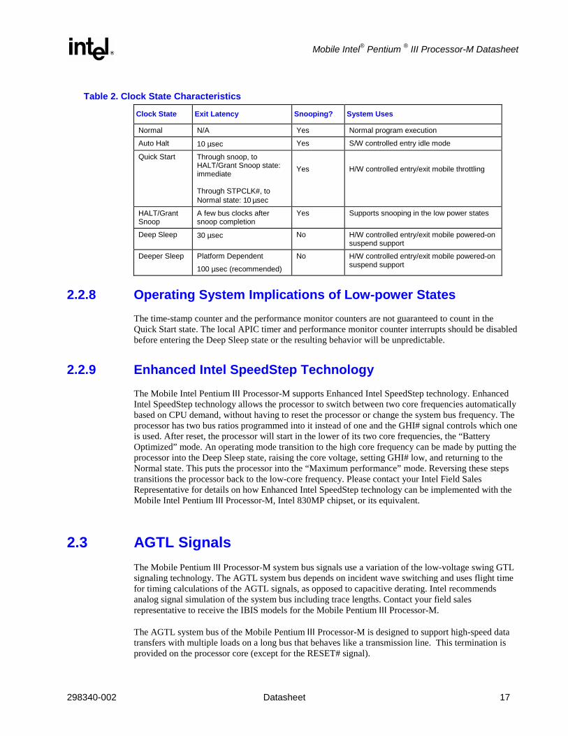
2.2.1 Clock Control Architecture The Mobile Pentium III Processor-M clock control architecture (Figure 1) has been optimized for leading edge mobile computer designs. The clock control architecture consists of six different clock states: Normal, Auto Halt, Quick Start, HALT/Grant Snoop, Deep Sleep and Deeper Sleep states. The Auto Halt state provides a low-power clock state that can be controlled through the software execution of the HLT instruction. The Quick Start state provides a very low power and low exit latency clock state that can be used for hardware controlled “idle” computer states. The Deep Sleep and Deeper Sleep states provide extremely low-power states that can be used for “Power-On-Suspend” computer states, which is an alternative to shutting off the processor’s power. The exit latency of the Deep Sleep state is 30 µsec in the Mobile Pentium III Processor-M. Performing state transitions not shown in Figure 1 is neither recommended nor supported. Table 2 provides the clock state characteristics, which are described in detail in the following sections.
2.2.2 Normal State The Normal state of the processor is the normal operating mode where the processor’s core clock is running and the processor is actively executing instructions.
2.2.3 Auto Halt State This is a low-power mode entered by the processor through the execution of the HLT instruction. A transition to the Normal state is made by a halt break event (one of the following signals going active: NMI, INTR, BINIT#, INIT#, RESET#, FLUSH#, or SMI#).

Mobile Intel® Pentium ® III Processor-M Datasheet
298340-002 Datasheet 15
Asserting the STPCLK# signal while in the Auto Halt state will cause the processor to transition to the Quick Start state. Deasserting STPCLK# will cause the processor to return to the Auto Halt state without issuing a new Halt bus cycle.
The SMI# interrupt is recognized in the Auto Halt state. The return from the System Management Interrupt (SMI) handler can be to either the Normal state or the Auto Halt state. See the Intel® Architecture Software Developer’s Manual, Volume III: System Programmer’s Guide for more information. No Halt bus cycle is issued when returning to the Auto Halt state from the System Management Mode (SMM).
The FLUSH# signal is serviced in the Auto Halt state. After the on-chip and off-chip caches have been flushed, the processor will return to the Auto Halt state without issuing a Halt bus cycle. Transitions in the A20M# and PREQ# signals are recognized while in the Auto Halt state.
Figure 1. Clock Control States
Quick StartNormalHS=false Deep Sleep 2
HALT/GrantSnoop
Auto HaltHS=true
DeeperSleep
STPCLK# 1 BCLK stoppedor DPSLP#
snoopoccurs
BCLK onand !DPSLP#
(!STPCLK# and !HS)or RESET#
snoopserviced
HLTinstruction 1
snoopserviced snoop
occurs
corevoltageraised
corevoltagereduced
STPCLK#1
!STPCLK#and HS
haltbreak
V0001-02
NOTES: 1. State transition does not occur until the Stop Grant or Auto Halt acknowledge bus cycle completes Halt break – A20M#, BINIT#, FLUSH#, INIT#, INTR, NMI, PREQ#, RESET#, SMI#, or APIC interrupt HLT – HLT instruction executed HS – Processor Halt State 2. Restrictions apply to the use of both methods of entering Deep Sleep. See Deep Sleep state description
for details.
2.2.4 Quick Start State The processor is required to be configured for the Quick Start state by strapping the A15# signal low. More details are provided in Section 7.1. In the Quick Start state the processor is only capable of acting on snoop transactions generated by the system bus priority device. Because of its snooping behavior, Quick Start can only be used in a uniprocessor (UP) configuration.

Mobile Intel® Pentium® III Processor-M Datasheet
16 Datasheet 298340-002
A transition to the Deep Sleep state can be made by stopping the clock input to the processor or asserting the DPSLP# signal. A transition back to the Normal state (from the Quick Start state) is made only if the STPCLK# signal is deasserted.
While in the Quick Start state the processor is limited in its ability to respond to input. It is incapable of latching any interrupts, servicing snoop transactions from symmetric bus masters or responding to FLUSH# or BINIT# assertions. While the processor is in the Quick Start state, it will not respond properly to any input signal other than STPCLK#, RESET#, or BPRI#. If any other input signal changes, then the behavior of the processor will be unpredictable. No serial interrupt messages may begin or be in progress while the processor is in the Quick Start state.
RESET# assertion will cause the processor to immediately initialize itself, but the processor will stay in the Quick Start state after initialization until STPCLK# is deasserted.
2.2.5 HALT/Grant Snoop State The processor will respond to snoop transactions on the system bus while in the Auto Halt or Quick Start state. When a snoop transaction is presented on the system bus the processor will enter the HALT/Grant Snoop state. The processor will remain in this state until the snoop has been serviced and the system bus is quiet. After the snoop has been serviced, the processor will return to its previous state. If the HALT/Grant Snoop state is entered from the Quick Start state, then the input signal restrictions of the Quick Start state still apply in the HALT/Grant Snoop state, except for those signal transitions that are required to perform the snoop.
2.2.6 Deep Sleep State The Deep Sleep state is a very low power state the processor can enter while maintaining its context. The Deep Sleep state is entered by stopping the BCLK and BCLK# inputs to the processor or by asserting the DPSLP# signal, while it is in the Quick Start state. Note that either one of the methods can be used to enter Deep Sleep but not both at the same time. When BCLK and BCLK# are stopped, they must obey the DC levels specified in Table 30 and Table 31.
The processor will return to the Quick Start state from the Deep Sleep state when the BCLK and BCLK# inputs are restarted or the DPSLP# signal is deasserted. Due to the PLL lock latency, there is a delay of up to 30 µsec after the clocks have started before this state transition happens. PICCLK may be removed in the Deep Sleep state. PICCLK should be designed to turn on when BCLK and BCLK# turn on or DPSLP# is deasserted when transitioning out of the Deep Sleep state.
2.2.7 Deeper Sleep State The Deeper Sleep state is the lowest power state the processor can enter while maintaining its context. It is functionally identical to the Deep Sleep State but at a lower voltage. The processor transitions to the Deeper Sleep state from the Deep Sleep when the voltage regulator lowers the core voltage. The VID signals for the Deeper Sleep State are supplied to the voltage regulator through control from the I/O Controller Hub component. For more details on how this is implemented on the Mobile Intel Pentium III Processor-M /Intel 830M platform, please refer to the Intel® 82801CAM I/O Controller Hub 3 (ICH3-M) Datasheet and contact your Intel Field Sales Representative for details on Intel Mobile Voltage Positioning – II (IMVP-II) implementation. For details on how Deeper Sleep is implemented on 440MX chipset based systems using the Intel SpeedStep technology Control Logic Plus (ISSCL+) component, please refer to the Mobile Intel® Pentium® III Processor-M/440MX Platform Design Guide.
Mobile Intel® Pentium ® III Processor-M Datasheet
298340-002 Datasheet 17
Table 2. Clock State Characteristics
Clock State Exit Latency Snooping? System Uses
Normal N/A Yes Normal program execution
Auto Halt 10 µsec Yes S/W controlled entry idle mode
Quick Start Through snoop, to HALT/Grant Snoop state: immediate Through STPCLK#, to Normal state: 10 µsec
Yes
H/W controlled entry/exit mobile throttling
HALT/Grant Snoop
A few bus clocks after snoop completion
Yes Supports snooping in the low power states
Deep Sleep 30 µsec No H/W controlled entry/exit mobile powered-on suspend support
Deeper Sleep Platform Dependent
100 µsec (recommended)
No H/W controlled entry/exit mobile powered-on suspend support
2.2.8 Operating System Implications of Low-power States The time-stamp counter and the performance monitor counters are not guaranteed to count in the Quick Start state. The local APIC timer and performance monitor counter interrupts should be disabled before entering the Deep Sleep state or the resulting behavior will be unpredictable.
2.2.9 Enhanced Intel SpeedStep Technology The Mobile Intel Pentium III Processor-M supports Enhanced Intel SpeedStep technology. Enhanced Intel SpeedStep technology allows the processor to switch between two core frequencies automatically based on CPU demand, without having to reset the processor or change the system bus frequency. The processor has two bus ratios programmed into it instead of one and the GHI# signal controls which one is used. After reset, the processor will start in the lower of its two core frequencies, the “Battery Optimized” mode. An operating mode transition to the high core frequency can be made by putting the processor into the Deep Sleep state, raising the core voltage, setting GHI# low, and returning to the Normal state. This puts the processor into the “Maximum performance” mode. Reversing these steps transitions the processor back to the low-core frequency. Please contact your Intel Field Sales Representative for details on how Enhanced Intel SpeedStep technology can be implemented with the Mobile Intel Pentium III Processor-M, Intel 830MP chipset, or its equivalent.
2.3 AGTL Signals The Mobile Pentium III Processor-M system bus signals use a variation of the low-voltage swing GTL signaling technology. The AGTL system bus depends on incident wave switching and uses flight time for timing calculations of the AGTL signals, as opposed to capacitive derating. Intel recommends analog signal simulation of the system bus including trace lengths. Contact your field sales representative to receive the IBIS models for the Mobile Pentium III Processor-M.
The AGTL system bus of the Mobile Pentium III Processor-M is designed to support high-speed data transfers with multiple loads on a long bus that behaves like a transmission line. This termination is provided on the processor core (except for the RESET# signal).

Mobile Intel® Pentium® III Processor-M Datasheet
18 Datasheet 298340-002
2.4 Mobile Intel Pentium III Processor-M CPUID When the CPUID version information is loaded with EAX=01H, the EAX and EBX registers contain the values shown in Table 3. After a power-on RESET, the EDX register contains the processor version information (type, family, model, stepping). Please refer to the Intel Processor Identification and the CPUID Instruction Application Note AP-485 for more details. Table 4 shows the CPUID Cache and TLB descriptor values after the L2 cache is initialized.
Table 3. Mobile Pentium III Processor-M CPUID
EAX[31:0] EBX[7:0]
Reserved [31:14] Type [13:12] Family [11:8] Model [7:4] Stepping [3:0] Brand ID
X 0 6 B X 06
Table 4. Mobile Pentium III Processor-M CPUID Cache and TLB Descriptors Cache and TLB Descriptors 01H, 02H, 03H, 04H, 08H, 0CH, 83H

Mobile Intel® Pentium ® III Processor-M Datasheet
298340-002 Datasheet 19
3. Electrical Specifications
3.1 Processor System Signals Table 5 lists the processor system signals by type. All AGTL signals are synchronous with the BCLK and BCLK# signals. All TAP signals are synchronous with the TCK signal except TRST#. All CMOS input signals can be applied asynchronously.
Table 5. System Signal Groups
Group Name Signals
AGTL Input BPRI#, DEFER#, RESET#, RSP#
AGTL Output PRDY#
AGTL I/O A[35:3]#, ADS#, AERR#, AP[1:0]#, BERR#, BINIT#, BNR#, BP[3:2]#, BPM[1:0]#, BREQ0#, D[63:0]#, DBSY#, DEP[7:0]#, DRDY#, HIT#, HITM#, LOCK#, REQ[4:0]#, RP#, RS[2:0]#, TRDY#
1.5V CMOS Input A20M#, DPSLP#, FLUSH#, IGNNE#, INIT#, LINT0/INTR, LINT1/NMI, PREQ#, SMI#, STPCLK#
1.8V CMOS Input PWRGOOD
1.5V Open Drain Output FERR#, IERR#
3.3V Open Drain Output BSEL[1:0], VID[4:0]
1.25V input GHI#, VTTPWRGD
Clock BCLK, BCLK# (Differential Mode)
2.5V Clock Input BCLK (Single Ended Mode)
APIC Clock PICCLK
APIC I/O PICD[1:0]
Thermal Diode THERMDC, THERMDA
TAP Input TCK, TDI, TMS, TRST#
TAP Output TDO
Power/Other CLKREF, CMOSREF, EDGECTRLP, NC, NCTRL, PLL1, PLL2, RTTIMPEDP, VCC, VCCT, VREF, VSS,
NOTES: 1. VCC is the power supply for the core logic. 2. PLL1 and PLL2 are power/ground for the PLL analog section. See section 3.2.2 for details. 3. VCCT is the power supply for the system bus buffers. 4. VREF is the voltage reference for the AGTL input buffers. 5. VSS is system ground.
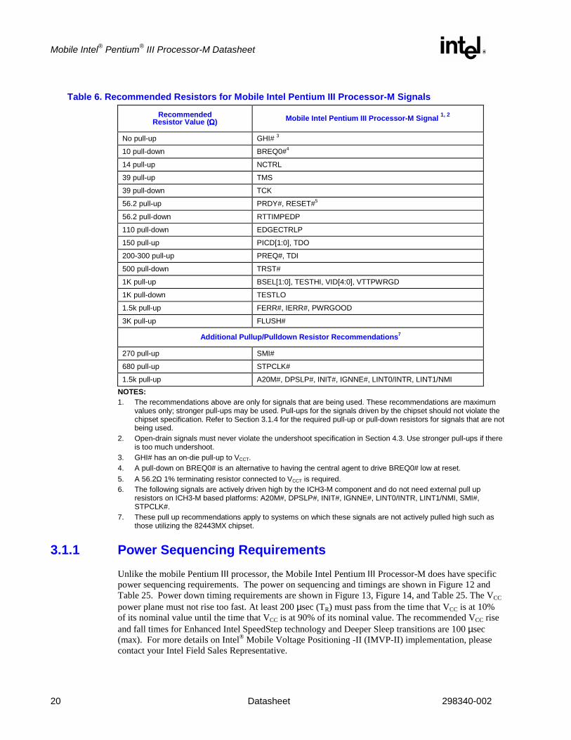
The APIC data and TAP outputs are Open-drain and should be pulled up to 1.5V using resistors with the values shown in Table 6. If Open-drain drivers are used for input signals, then they should also be pulled up to the appropriate voltage using resistors with the values shown in Table 6.
Mobile Intel® Pentium® III Processor-M Datasheet
20 Datasheet 298340-002
Table 6. Recommended Resistors for Mobile Intel Pentium III Processor-M Signals
Recommended Resistor Value (ΩΩΩΩ) Mobile Intel Pentium III Processor-M Signal 1, 2
No pull-up GHI# 3
10 pull-down BREQ0#4
14 pull-up NCTRL
39 pull-up TMS
39 pull-down TCK
56.2 pull-up PRDY#, RESET#5
56.2 pull-down RTTIMPEDP
110 pull-down EDGECTRLP
150 pull-up PICD[1:0], TDO
200-300 pull-up PREQ#, TDI
500 pull-down TRST#
1K pull-up BSEL[1:0], TESTHI, VID[4:0], VTTPWRGD
1K pull-down TESTLO
1.5k pull-up FERR#, IERR#, PWRGOOD
3K pull-up FLUSH#
Additional Pullup/Pulldown Resistor Recommendations7
270 pull-up SMI#
680 pull-up STPCLK#
1.5k pull-up A20M#, DPSLP#, INIT#, IGNNE#, LINT0/INTR, LINT1/NMI NOTES: 1. The recommendations above are only for signals that are being used. These recommendations are maximum
values only; stronger pull-ups may be used. Pull-ups for the signals driven by the chipset should not violate the chipset specification. Refer to Section 3.1.4 for the required pull-up or pull-down resistors for signals that are not being used.
2. Open-drain signals must never violate the undershoot specification in Section 4.3. Use stronger pull-ups if there is too much undershoot.
3. GHI# has an on-die pull-up to VCCT. 4. A pull-down on BREQ0# is an alternative to having the central agent to drive BREQ0# low at reset. 5. A 56.2Ω 1% terminating resistor connected to VCCT is required. 6. The following signals are actively driven high by the ICH3-M component and do not need external pull up
resistors on ICH3-M based platforms: A20M#, DPSLP#, INIT#, IGNNE#, LINT0/INTR, LINT1/NMI, SMI#, STPCLK#.
7. These pull up recommendations apply to systems on which these signals are not actively pulled high such as those utilizing the 82443MX chipset.
3.1.1 Power Sequencing Requirements Unlike the mobile Pentium III processor, the Mobile Intel Pentium III Processor-M does have specific power sequencing requirements. The power on sequencing and timings are shown in Figure 12 and Table 25. Power down timing requirements are shown in Figure 13, Figure 14, and Table 25. The VCC power plane must not rise too fast. At least 200 µsec (TR) must pass from the time that VCC is at 10% of its nominal value until the time that VCC is at 90% of its nominal value. The recommended VCC rise and fall times for Enhanced Intel SpeedStep technology and Deeper Sleep transitions are 100 µsec (max). For more details on Intel® Mobile Voltage Positioning -II (IMVP-II) implementation, please contact your Intel Field Sales Representative.

Mobile Intel® Pentium ® III Processor-M Datasheet
298340-002 Datasheet 21
3.1.2 Test Access Port (TAP) Connection The TAP interface is an implementation of the IEEE 1149.1 (“JTAG”) standard. Due to the voltage levels supported by the TAP interface, Intel recommends that the Mobile Intel Pentium III Processor-M and the other 1.5-V JTAG specification compliant devices be last in the JTAG chain after any devices with 3.3-V or 5.0-V JTAG interfaces within the system. A translation buffer should be used to reduce the TDO output voltage of the last 3.3/5.0V device down to the 1.5V range that the Mobile Intel Pentium III Processor-M can tolerate. Multiple copies of TMS and TRST# must be provided, one for each voltage level.
A Debug Port and connector may be placed at the start and end of the JTAG chain containing the processor, with TDI to the first component coming from the Debug Port and TDO from the last component going to the Debug Port. There are no requirements for placing the Mobile Intel Pentium III Processor-M in the JTAG chain, except for those that are dictated by voltage requirements of the TAP signals.
3.1.3 Catastrophic Thermal Protection The Mobile Intel Pentium III Processor-M does not support catastrophic thermal protection or the THERMTRIP# signal. An external thermal sensor must be used to protect the processor and the system against excessive temperatures. If the external thermal sensor detects a processor junction temperature of 101°C (maximum), both the VCC and VCCT supplies to the processor must be reduced to at least 50% of the nominal values within 500 ms and recommended to be turned off completely within 1s to prevent damage to the processor. Processor temperature must be monitored in all states including low power states.
3.1.4 Unused Signals All signals named NC must be unconnected. Unused AGTL inputs, outputs and bi-directional signals should be unconnected. Unused CMOS active low inputs should be connected to 1.5V and unused active high inputs should be connected to VSS. Unused Open-drain outputs should be unconnected. When tying any signal to power or ground, a resistor will allow for system testability. For unused signals, Intel suggests that 1.5-kΩ resistors are used for pull-ups and 1.0-kΩ resistors are used for pull-downs.
PICCLK must be driven with a clock that meets specification and the PICD[1:0] signals must be pulled up separately to 1.5V with 150-Ω resistors, even if the local APIC is not used.
If the TAP signals are not used then the inputs should be pulled to ground with 1-kΩ resistors and TDO should be left unconnected.
3.1.5 Signal State in Low-power States
3.1.5.1 System Bus Signals All of the system bus signals have AGTL input, output, or input/output drivers. Except when servicing snoops, the system bus signals are tri-stated and pulled up by the termination resistors. Snoops are not permitted in the Deep Sleep and Deeper Sleep states.

Mobile Intel® Pentium® III Processor-M Datasheet
22 Datasheet 298340-002
3.1.5.2 CMOS and Open-drain Signals The CMOS input signals are allowed to be in either the logic high or low state when the processor is in a low-power state. In the Auto Halt state these signals are allowed to toggle. These input buffers have no internal pull-up or pull-down resistors and system logic can use CMOS or Open-drain drivers to drive them.
The Open-drain output signals have open drain drivers and external pull-up resistors are required. One of the two output signals (IERR#) is a catastrophic error indicator and is tri-stated (and pulled-up) when the processor is functioning normally. The FERR# output can be either tri-stated or driven to VSS when the processor is in a low-power state depending on the condition of the floating-point unit. Since this signal is a DC current path when it is driven to VSS, Intel recommends that the software clears or masks any floating-point error condition before putting the processor into the Deep Sleep state.
3.1.5.3 Other Signals The system bus clocks (BCLK, BCLK#) must be driven in all of the low-power states except the Deep Sleep state. The APIC clock (PICCLK) must be driven whenever BCLK and BCLK# are driven. Otherwise, it is permitted to turn off PICCLK by holding it at VSS. BCLK and BCLK# should be obey the DC levels in Table 30(for Differential Clocking) and Table 31 (for Single Ended Clocking).
In the Auto Halt state, the APIC bus data signals (PICD[1:0]) may toggle due to APIC bus messages. These signals are required to be tri-stated and pulled-up when the processor is in the Quick Start or Deep Sleep states.
3.2 Power Supply Requirements
3.2.1 Decoupling Guidelines The Mobile Intel Pentium III Processor-M Micro-FCPGA package has twelve 0805IDC, 1-µF surface mount decoupling capacitors. Eight capacitors are on the VCC supply and four capacitors are on VCCT. For the Micro-FCBGA package, there are six 0.68-µF capacitors on VCC and two 0.68-µF capacitors on VCCT . In addition to the package capacitors, sufficient board level capacitors are also necessary for power supply decoupling. These guidelines are as follows:
• High and Mid Frequency VCC decoupling – Place twenty-four 0.22-µF 0603 capacitors directly under the package on the solder side of the motherboard using at least two vias per capacitor node. Ten 10-µF X7 6.3V 1206-size ceramic capacitors should be placed around the package periphery near the balls. Trace lengths to the vias should be designed to minimize inductance. Avoid bending traces to minimize ESL.
• High and Mid Frequency VCCT decoupling – Place ten 1-µF X7R 0603 ceramic capacitors close to the package. Via and trace guidelines are the same as above.
• Bulk VCC decoupling – Minimum of 1200 µF capacitance with Equivalent Series Resistance (ESR) less than or equal to 3.5 mΩ.
• Bulk VCCT decoupling – Platform dependent but recommendation for Intel® 830 Chipset Family based systems is minimum of 660 µF with ESR less than or equal to 7 mΩ.
Mobile Intel® Pentium ® III Processor-M Datasheet
298340-002 Datasheet 23
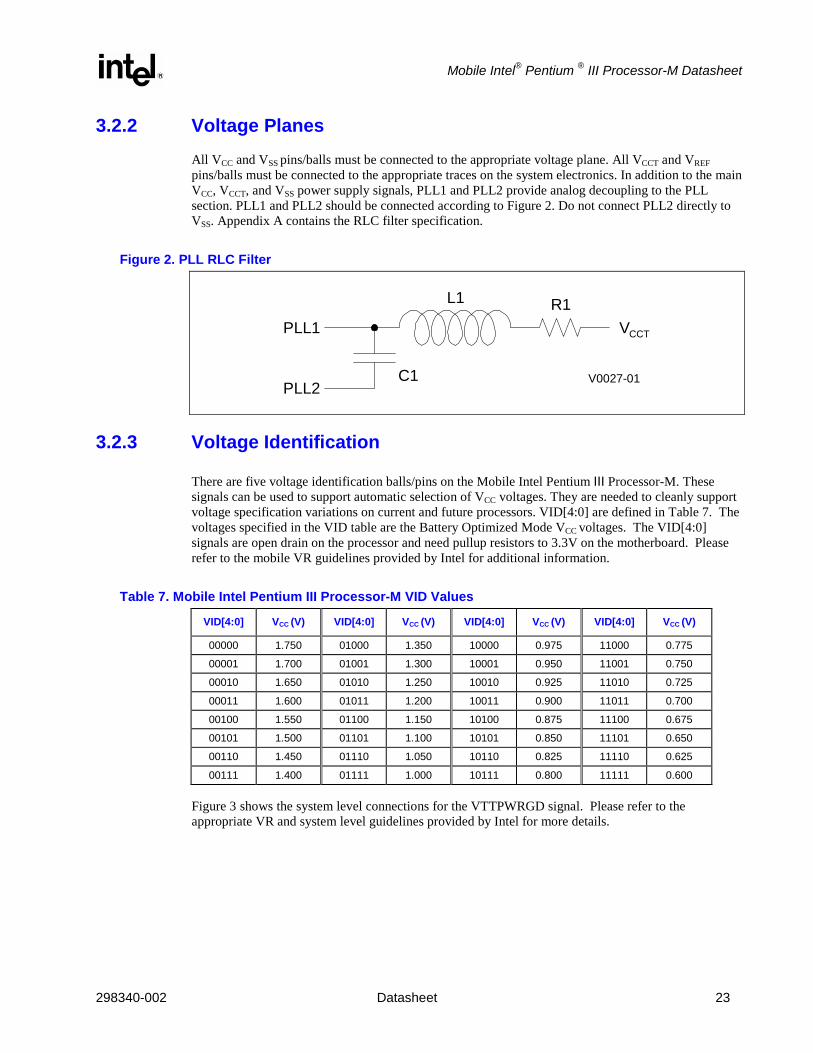
3.2.2 Voltage Planes All VCC and VSS pins/balls must be connected to the appropriate voltage plane. All VCCT and VREF pins/balls must be connected to the appropriate traces on the system electronics. In addition to the main VCC, VCCT, and VSS power supply signals, PLL1 and PLL2 provide analog decoupling to the PLL section. PLL1 and PLL2 should be connected according to Figure 2. Do not connect PLL2 directly to VSS. Appendix A contains the RLC filter specification.
Figure 2. PLL RLC Filter
PLL1
PLL2
VCCT
V0027-01
L1
C1
R1
3.2.3 Voltage Identification
There are five voltage identification balls/pins on the Mobile Intel Pentium III Processor-M. These signals can be used to support automatic selection of VCC voltages. They are needed to cleanly support voltage specification variations on current and future processors. VID[4:0] are defined in Table 7. The voltages specified in the VID table are the Battery Optimized Mode VCC voltages. The VID[4:0] signals are open drain on the processor and need pullup resistors to 3.3V on the motherboard. Please refer to the mobile VR guidelines provided by Intel for additional information.
Table 7. Mobile Intel Pentium III Processor-M VID Values
VID[4:0] VCC (V) VID[4:0] VCC (V) VID[4:0] VCC (V) VID[4:0] VCC (V)
00000 1.750 01000 1.350 10000 0.975 11000 0.775
00001 1.700 01001 1.300 10001 0.950 11001 0.750
00010 1.650 01010 1.250 10010 0.925 11010 0.725
00011 1.600 01011 1.200 10011 0.900 11011 0.700
00100 1.550 01100 1.150 10100 0.875 11100 0.675
00101 1.500 01101 1.100 10101 0.850 11101 0.650
00110 1.450 01110 1.050 10110 0.825 11110 0.625
00111 1.400 01111 1.000 10111 0.800 11111 0.600
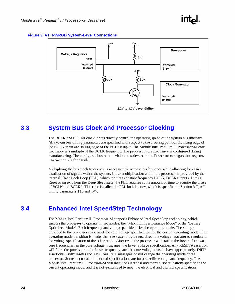
Figure 3 shows the system level connections for the VTTPWRGD signal. Please refer to the appropriate VR and system level guidelines provided by Intel for more details.
Mobile Intel® Pentium® III Processor-M Datasheet
24 Datasheet 298340-002
Figure 3. VTTPWRGD System-Level Connections
Voltage RegulatorProcessor
Clock Generator
Vcct
Vttpwrgd(output)
Vttpwrgd(input)
Vttpwrgd#(input)
Vcct
10k
Vcct
3.3V
100k
1.2V to 3.3V Level Shifter
1k
3.3 System Bus Clock and Processor Clocking The BCLK and BCLK# clock inputs directly control the operating speed of the system bus interface. All system bus timing parameters are specified with respect to the crossing point of the rising edge of the BCLK input and falling edge of the BCLK# input. The Mobile Intel Pentium III Processor-M core frequency is a multiple of the BCLK frequency. The processor core frequency is configured during manufacturing. The configured bus ratio is visible to software in the Power-on configuration register. See Section 7.2 for details.
Multiplying the bus clock frequency is necessary to increase performance while allowing for easier distribution of signals within the system. Clock multiplication within the processor is provided by the internal Phase Lock Loop (PLL), which requires constant frequency BCLK, BCLK# inputs. During Reset or on exit from the Deep Sleep state, the PLL requires some amount of time to acquire the phase of BCLK and BCLK#. This time is called the PLL lock latency, which is specified in Section 3.7, AC timing parameters T18 and T47.
3.4 Enhanced Intel SpeedStep Technology The Mobile Intel Pentium III Processor-M supports Enhanced Intel SpeedStep technology, which enables the processor to operate in two modes, the “Maximum Performance Mode” or the “Battery Optimized Mode”. Each frequency and voltage pair identifies the operating mode. The voltage provided to the processor must meet the core voltage specification for the current operating mode. If an operating mode transition is made, then the system logic must direct the voltage regulator to regulate to the voltage specification of the other mode. After reset, the processor will start in the lower of its two core frequencies, so the core voltage must meet the lower voltage specification. Any RESET# assertion will force the processor to the lower frequency, and the core voltage must behave appropriately. INIT# assertions ("soft" resets) and APIC bus INIT messages do not change the operating mode of the processor. Some electrical and thermal specifications are for a specific voltage and frequency. The Mobile Intel Pentium III Processor-M will meet the electrical and thermal specifications specific to the current operating mode, and it is not guaranteed to meet the electrical and thermal specifications

Mobile Intel® Pentium ® III Processor-M Datasheet
298340-002 Datasheet 25
specific to the opposite operating mode. The timing specifications must be met when performing an operating mode transition.
3.5 Maximum Ratings Table 8 contains the Mobile Intel Pentium III Processor-M stress ratings. Functional operation at the absolute maximum and minimum is neither implied nor guaranteed. The processor should not receive a clock while subjected to these conditions. Functional operating conditions are provided in the AC and DC tables. Extended exposure to the maximum ratings may affect device reliability. Furthermore, although the processor contains protective circuitry to resist damage from static electric discharge, one should always take precautions to avoid high static voltages or electric fields.
Table 8. Mobile Intel Pentium III Processor-M Absolute Maximum Ratings
Symbol Parameter Min Max Unit Notes
TStorage Storage Temperature –40 85 °C Note 1
VCC(Abs) Supply Voltage with respect to VSS –0.5 1.75 V
VCCT System Bus Buffer Voltage with respect to VSS –0.3 1.75 V
VIN GTL System Bus Buffer DC Input Voltage with respect to VSS –0.3 1.75 V Notes 2, 3
VIN125 1.25V Buffer DC Input Voltage with respect to VSS –0.3 1.75 V Note 4
VIN15 1.5V Buffer DC Input Voltage with respect to VSS –0.3 2.0 V Note 5
VIN18 1.8V Buffer DC Input Voltage with respect to VSS –0.3 2.0 V Note 6
VIN20 2.0V Buffer DC Input Voltage with respect to VSS –0.3 2.4 V Note 7
VIN25 2.5V Buffer DC Input Voltage with respect to VSS –0.3 3.3 V Note 9
VINVID VID ball/pin DC Input Voltage with respect to VSS — 3.465 V Note 8
IVID VID Current -0.3 3.6 mA Note 8 NOTES: 1. The shipping container is only rated for 65°C. 2. Parameter applies to the AGTL signal groups only. Compliance with both VIN GTL specifications is required. 3. The voltage on the AGTL signals must never be below –0.3 or above 1.75V with respect to ground. 4. Parameter applies to CLKREF, GHI#, TESTHI, VTTPWRGD signals. 5. Parameter applies to CMOS, Open-drain, APIC, TESTLO and TAP bus signal groups only. 6. Parameter applies to PWRGOOD signal. 7. Parameter applies to PICCLK signal. 8. Parameter applies to each VID pin/ball individually. 9. Parameter applies to BCLK signal in Single Ended Clocking Mode.
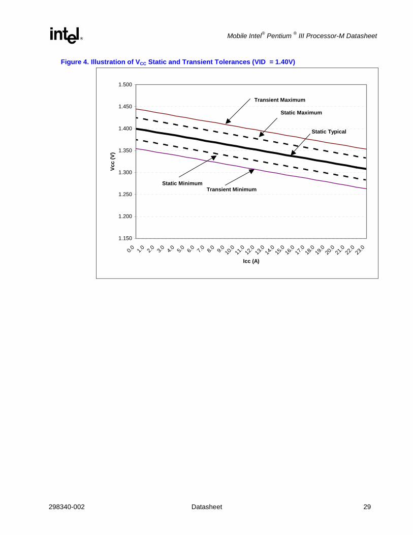
3.6 DC Specifications Table 9 through Table 18 list the DC specifications for the Mobile Intel Pentium III Processor-M. Specifications are valid only while meeting specifications for the junction temperature, clock frequency, and input voltages. The junction temperature range for all DC specifications is 0°C to 100°C. Care should be taken to read all notes associated with each parameter. Unlike the mobile Pentium III processor, the Vcc tolerances for the Mobile Intel Pentium III Processor-M are not specified as a percentage of nominal. The tolerances are instead specified in the form of load lines for the static and transient cases in Table 10 through Table 15. Illustration of the load lines is shown in Figure 4 and Figure 5.

Mobile Intel® Pentium® III Processor-M Datasheet
26 Datasheet 298340-002
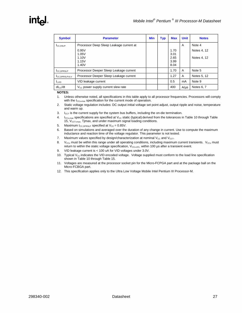
Table 9. Power Specifications for Mobile Intel Pentium III Processor-M1
Symbol Parameter Min Typ Max Unit Notes
VCC Transient VCC for core logic Battery Optimized Mode Maximum Performance Mode
0.95 1.05 1.15 1.10 1.15 1.40
V
Notes 10, 11
VCC,DC Static VCC for core logic Battery Optimized Mode Maximum Performance Mode
0.95 1.05 1.15 1.10 1.15 1.40
V
Notes 10, 11
VCCDPRSLP Transient VCC for core logic during Deeper Sleep 0.785 0.85 0.900 V Note 11
VCCDPRSLP, DC Static VCC for core logic during Deeper Sleep 0.80 0.85 0.880 V Note 11
VCCT VCC for System Bus Buffers, Transient tolerance 1.138 1.25 1.362 V ± 9%, Notes 8,11
VCCT,DC VCC for System Bus Buffers, Static tolerance 1.188 1.25 1.312 V ±5%, Notes 2,11
ICC Current for VCC at core frequency 300 MHz & 0.95V 450 MHz & 1.05V 466 MHz & 1.05V 500 MHz & 1.05V 533 MHz & 1.05V 700 MHz & 1.10V 667 MHz & 1.15V 733 MHz & 1.15V 750 MHz & 1.15V 800 MHz & 1.15V 866 MHz & 1.40V 933 MHz & 1.40V 1000 MHz & 1.40V 1066 MHz & 1.40V 1133 MHz & 1.40V 1200 MHz & 1.40V
3.58 6.08 6.19 6.38 6.61 7.58 8.90 9.39 9.47 9.8415.87 16.45 16.83 17.46 18.11 18.27
A
Note 4 Notes 4, 12 Notes 4, 12
ICCT Current for VCCT 2.7 A Notes 3, 4
ICC,AH Processor Auto Halt current at 0.95V 1.05V 1.10V 1.15V 1.40V
1.88 3.36 3.09 4.52 8.85
A Note 4 Notes 4, 12 Notes 4, 12
ICC,QS Processor Quick Start current at 0.95V 1.05V 1.10V 1.15V 1.40V
1.82 3.22 2.91 4.30 8.53
A Note 4 Notes 4, 12 Notes 4, 12
Mobile Intel® Pentium ® III Processor-M Datasheet
298340-002 Datasheet 27
Symbol Parameter Min Typ Max Unit Notes
ICC,DSLP Processor Deep Sleep Leakage current at 0.95V 1.05V 1.10V 1.15V 1.40V
1.70 3.01 2.65 3.99 8.04
A Note 4 Notes 4, 12 Notes 4, 12
ICC,DPRSLP Processor Deeper Sleep Leakage current 1.70 A Note 5
ICC,DPRSLPULV Processor Deeper Sleep Leakage current 1.27 A Notes 5, 12
ILVID VID leakage current 0.5 mA Note 9
dICC/dt VCC power supply current slew rate 400 A/µs Notes 6, 7 NOTES: 1. Unless otherwise noted, all specifications in this table apply to all processor frequencies. Processors will comply
with the ICCx,max specification for the current mode of operation. 2. Static voltage regulation includes: DC output initial voltage set point adjust, output ripple and noise, temperature
and warm up. 3. ICCT is the current supply for the system bus buffers, including the on-die termination. 4. ICCx,max specifications are specified at VCC static (typical) derived from the tolerances in Table 10 through Table
15, VCCT,max, Tjmax, and under maximum signal loading conditions. 5. Maximum ICC,DPRSLP specified at VCC = 0.85V. 6. Based on simulations and averaged over the duration of any change in current. Use to compute the maximum
inductance and reaction time of the voltage regulator. This parameter is not tested. 7. Maximum values specified by design/characterization at nominal VCC and VCCT. 8. VCCx must be within this range under all operating conditions, including maximum current transients. VCCx must
return to within the static voltage specification, VCCx,DC, within 100 µs after a transient event. 9. VID leakage current is < 100 uA for VID voltages under 3.0V. 10. Typical VCC indicates the VID encoded voltage. Voltage supplied must conform to the load line specification
shown in Table 10 through Table 15. 11. Voltages are measured at the processor socket pin for the Micro-FCPGA part and at the package ball on the
Micro-FCBGA part. 12. This specification applies only to the Ultra Low Voltage Mobile Intel Pentium III Processor-M.
Mobile Intel® Pentium® III Processor-M Datasheet
28 Datasheet 298340-002
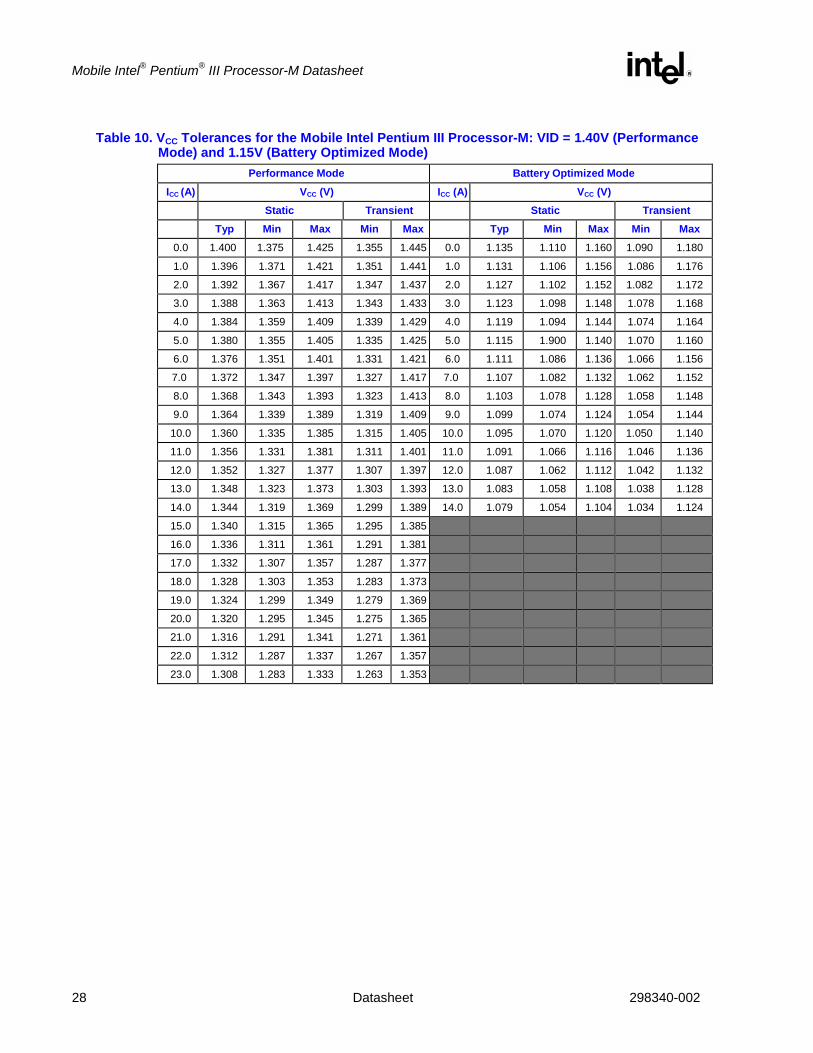
Table 10. VCC Tolerances for the Mobile Intel Pentium III Processor-M: VID = 1.40V (Performance Mode) and 1.15V (Battery Optimized Mode)
Performance Mode Battery Optimized Mode ICC (A) VCC (V) ICC (A) VCC (V)
Static Transient Static Transient Typ Min Max Min Max Typ Min Max Min Max
0.0 1.400 1.375 1.425 1.355 1.445 0.0 1.135 1.110 1.160 1.090 1.180
1.0 1.396 1.371 1.421 1.351 1.441 1.0 1.131 1.106 1.156 1.086 1.176
2.0 1.392 1.367 1.417 1.347 1.437 2.0 1.127 1.102 1.152 1.082 1.172
3.0 1.388 1.363 1.413 1.343 1.433 3.0 1.123 1.098 1.148 1.078 1.168
4.0 1.384 1.359 1.409 1.339 1.429 4.0 1.119 1.094 1.144 1.074 1.164
5.0 1.380 1.355 1.405 1.335 1.425 5.0 1.115 1.900 1.140 1.070 1.160
6.0 1.376 1.351 1.401 1.331 1.421 6.0 1.111 1.086 1.136 1.066 1.156
7.0 1.372 1.347 1.397 1.327 1.417 7.0 1.107 1.082 1.132 1.062 1.152
8.0 1.368 1.343 1.393 1.323 1.413 8.0 1.103 1.078 1.128 1.058 1.148
9.0 1.364 1.339 1.389 1.319 1.409 9.0 1.099 1.074 1.124 1.054 1.144
10.0 1.360 1.335 1.385 1.315 1.405 10.0 1.095 1.070 1.120 1.050 1.140
11.0 1.356 1.331 1.381 1.311 1.401 11.0 1.091 1.066 1.116 1.046 1.136
12.0 1.352 1.327 1.377 1.307 1.397 12.0 1.087 1.062 1.112 1.042 1.132
13.0 1.348 1.323 1.373 1.303 1.393 13.0 1.083 1.058 1.108 1.038 1.128
14.0 1.344 1.319 1.369 1.299 1.389 14.0 1.079 1.054 1.104 1.034 1.124
15.0 1.340 1.315 1.365 1.295 1.385
16.0 1.336 1.311 1.361 1.291 1.381
17.0 1.332 1.307 1.357 1.287 1.377
18.0 1.328 1.303 1.353 1.283 1.373 19.0 1.324 1.299 1.349 1.279 1.369 20.0 1.320 1.295 1.345 1.275 1.365 21.0 1.316 1.291 1.341 1.271 1.361 22.0 1.312 1.287 1.337 1.267 1.357 23.0 1.308 1.283 1.333 1.263 1.353
Mobile Intel® Pentium ® III Processor-M Datasheet
298340-002 Datasheet 29
Figure 4. Illustration of VCC Static and Transient Tolerances (VID = 1.40V)
1.150
1.200
1.250
1.300
1.350
1.400
1.450
1.500
0.0 1.0 2.0 3.0 4.0 5.0 6.0 7.0 8.0 9.0 10.0
11.0
12.0
13.0
14.0
15.0
16.0
17.0
18.0
19.0
20.0
21.0
22.0
23.0
Icc (A)
Vcc
(V)
Transient Maximum
Static Maximum
Static Typical
Static MinimumTransient Minimum

Mobile Intel® Pentium® III Processor-M Datasheet
30 Datasheet 298340-002
Table 11. VCC Tolerances for the Mobile Intel Pentium III Processor-M in the Deep Sleep State: VID = 1.40V (Performance Mode) and 1.15V (Battery Optimized Mode)
Performance Mode Battery Optimized Mode ICC (A) VCC (V) ICC (A) VCC (V)
Static Transient Static Transient Typ Min Max Min Max Typ Min Max Min Max
0.0 1.338 1.313 1.363 1.293 1.383 0.0 1.084 1.059 1.109 1.039 1.129
1.0 1.334 1.309 1.359 1.289 1.379 1.0 1.080 1.055 1.105 1.035 1.125
2.0 1.330 1.305 1.355 1.285 1.375 2.0 1.076 1.051 1.101 1.031 1.121
3.0 1.326 1.301 1.351 1.281 1.371 3.0 1.072 1.047 1.097 1.027 1.117
4.0 1.322 1.297 1.347 1.277 1.367 4.0 1.068 1.043 1.093 1.023 1.113
5.0 1.318 1.293 1.343 1.273 1.363 5.0 1.064 1.039 1.089 1.019 1.109
6.0 1.314 1.289 1.339 1.269 1.359 6.0 1.060 1.035 1.085 1.015 1.105
7.0 1.310 1.285 1.335 1.265 1.355
8.0 1.306 1.281 1.331 1.261 1.351
Figure 5. Illustration of Deep Sleep VCC Static and Transient Tolerances (VID Setting = 1.40V)
1.180
1.230
1.280
1.330
1.380
1.430
0 1 2 3 4 5 6 7 8
Icc (A)
Vcc
(V)
Transient Maximum Static MaximumStatic Typical
Static MinimumTransient Minimum

Mobile Intel® Pentium ® III Processor-M Datasheet
298340-002 Datasheet 31
Table 12. VCC Tolerances for the Low Voltage Mobile Intel Pentium III Processor-M: VID = 1.15V (Performance Mode) and 1.05V (Battery Optimized Mode)
Performance Mode Battery Optimized Mode ICC (A) VCC (V) ICC (A) VCC (V)
Static Transient Static Transient Typ Min Max Min Max Typ Min Max Min Max
0.0 1.150 1.125 1.175 1.105 1.195 0.0 1.036 1.011 1.061 0.991 1.081
1.0 1.146 1.121 1.171 1.101 1.191 1.0 1.032 1.007 1.057 0.987 1.077
2.0 1.142 1.117 1.167 1.097 1.187 2.0 1.028 1.003 1.053 0.983 1.073
3.0 1.138 1.113 1.163 1.093 1.183 3.0 1.024 0.999 1.049 0.979 1.069
4.0 1.134 1.109 1.159 1.089 1.179 4.0 1.020 0.995 1.045 0.975 1.065
5.0 1.130 1.105 1.155 1.085 1.175 5.0 1.016 0.991 1.041 0.971 1.061
6.0 1.126 1.101 1.151 1.081 1.171 6.0 1.012 0.987 1.037 0.967 1.057
7.0 1.122 1.097 1.147 1.077 1.167 7.0 1.008 0.983 1.033 0.963 1.053
8.0 1.118 1.093 1.143 1.073 1.163 8.0 1.004 0.979 1.029 0.959 1.049
9.0 1.114 1.089 1.139 1.069 1.159 9.0 1.000 0.975 1.025 0.955 1.045
10.0 1.110 1.085 1.135 1.065 1.155 10.0 0.996 0.971 1.021 0.951 1.041
11.0 1.106 1.081 1.131 1.061 1.151
12.0 1.102 1.077 1.127 1.057 1.147
13.0 1.098 1.073 1.123 1.053 1.143
14.0 1.094 1.069 1.119 1.049 1.139
15.0 1.090 1.065 1.115 1.045 1.135
Table 13. VCC Tolerances for the Low Voltage Mobile Intel Pentium III Processor-M in the Deep Sleep State: VID = 1.15V (Performance Mode) and 1.05V (Battery Optimized Mode)
Performance Mode Battery Optimized Mode ICC (A) VCC (V) ICC (A) VCC (V)
Static Transient Static Transient Typ Min Max Min Max Typ Min Max Min Max
0.0 1.114 1.089 1.139 1.069 1.159 0.0 1.016 0.991 1.041 0.958 1.061
1.0 1.110 1.085 1.135 1.065 1.155 1.0 1.012 0.987 1.037 0.954 1.057
2.0 1.106 1.081 1.131 1.061 1.151 2.0 1.008 0.983 1.033 0.950 1.053
3.0 1.102 1.077 1.127 1.057 1.147 3.0 1.004 0.979 1.029 0.946 1.049
4.0 1.098 1.073 1.123 1.053 1.143 4.0 1.000 0.975 1.025 0.942 1.045
5.0 1.094 1.069 1.119 1.049 1.139 5.0 0.996 0.971 1.021 0.938 1.041
6.0 1.090 1.065 1.115 1.045 1.135
Mobile Intel® Pentium® III Processor-M Datasheet
32 Datasheet 298340-002
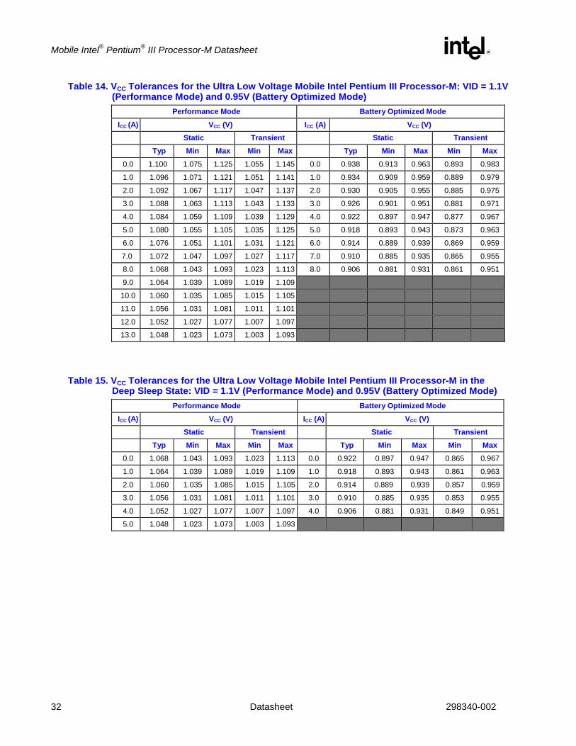
Table 14. VCC Tolerances for the Ultra Low Voltage Mobile Intel Pentium III Processor-M: VID = 1.1V (Performance Mode) and 0.95V (Battery Optimized Mode)
Performance Mode Battery Optimized Mode ICC (A) VCC (V) ICC (A) VCC (V)
Static Transient Static Transient Typ Min Max Min Max Typ Min Max Min Max
0.0 1.100 1.075 1.125 1.055 1.145 0.0 0.938 0.913 0.963 0.893 0.983
1.0 1.096 1.071 1.121 1.051 1.141 1.0 0.934 0.909 0.959 0.889 0.979
2.0 1.092 1.067 1.117 1.047 1.137 2.0 0.930 0.905 0.955 0.885 0.975
3.0 1.088 1.063 1.113 1.043 1.133 3.0 0.926 0.901 0.951 0.881 0.971
4.0 1.084 1.059 1.109 1.039 1.129 4.0 0.922 0.897 0.947 0.877 0.967
5.0 1.080 1.055 1.105 1.035 1.125 5.0 0.918 0.893 0.943 0.873 0.963
6.0 1.076 1.051 1.101 1.031 1.121 6.0 0.914 0.889 0.939 0.869 0.959
7.0 1.072 1.047 1.097 1.027 1.117 7.0 0.910 0.885 0.935 0.865 0.955
8.0 1.068 1.043 1.093 1.023 1.113 8.0 0.906 0.881 0.931 0.861 0.951
9.0 1.064 1.039 1.089 1.019 1.109
10.0 1.060 1.035 1.085 1.015 1.105
11.0 1.056 1.031 1.081 1.011 1.101
12.0 1.052 1.027 1.077 1.007 1.097
13.0 1.048 1.023 1.073 1.003 1.093
Table 15. VCC Tolerances for the Ultra Low Voltage Mobile Intel Pentium III Processor-M in the Deep Sleep State: VID = 1.1V (Performance Mode) and 0.95V (Battery Optimized Mode)
Performance Mode Battery Optimized Mode ICC (A) VCC (V) ICC (A) VCC (V)
Static Transient Static Transient Typ Min Max Min Max Typ Min Max Min Max
0.0 1.068 1.043 1.093 1.023 1.113 0.0 0.922 0.897 0.947 0.865 0.967
1.0 1.064 1.039 1.089 1.019 1.109 1.0 0.918 0.893 0.943 0.861 0.963
2.0 1.060 1.035 1.085 1.015 1.105 2.0 0.914 0.889 0.939 0.857 0.959
3.0 1.056 1.031 1.081 1.011 1.101 3.0 0.910 0.885 0.935 0.853 0.955
4.0 1.052 1.027 1.077 1.007 1.097 4.0 0.906 0.881 0.931 0.849 0.951
5.0 1.048 1.023 1.073 1.003 1.093
Mobile Intel® Pentium ® III Processor-M Datasheet
298340-002 Datasheet 33
Table 16. AGTL Signal Group DC Specifications
Symbol Parameter Min Max Unit Notes
VIL Input Low Voltage -0.15 VREF-0.2 V
VIH Input High Voltage VREF+0.2 VCCT V See VCCT,max in Table 17
VOH Output High Voltage — — V See VCCT,max in Table 17
RON Output Low Drive Strength 16.67 Ω Note 2
IL Leakage Current for Inputs, Outputs and I/Os 100 µA Note 1 NOTES: 1. Specification applies to leakage high only, for pins with on die RTT, (0 < VIN/OUT ≤ VCCT). 2. Refer to IBIS models for I/V characteristics.
Table 17. AGTL Bus DC Specifications
Symbol Parameter Min Typ Max Unit Notes
VCCT Bus Termination Voltage 1.25 V Note 1
VREF Input Reference Voltage 2/3VCCT – 2% 2/3VCCT2/3VCCT + 2% V ±2%, Note 2
RTT Bus Termination Strength 50 56 65 Ω On-die RTT, Note 3
NOTES: 1. Please refer to Table 9 for minimum and maximum values. 2. VREF should be created from VCCT by a voltage divider. 3. The RESET# signal does not have an on-die RTT. It requires an off-die 56.2Ω ±1% terminating resistor
connected to VCCT.

Mobile Intel® Pentium® III Processor-M Datasheet
34 Datasheet 298340-002
Table 18. CLKREF, APIC, TAP, CMOS, and Open-drain Signal Group DC Specifications
Symbol Parameter Min Max Unit Notes
VIL15 Input Low Voltage, 1.5V CMOS –0.15 VCMOSREFmin – 300 mV
V
VIL18 Input Low Voltage, 1.8V CMOS –0.36 0.36 V Notes 1, 2
VIH15 Input High Voltage, 1.5V CMOS VCMOSREFmax + 250 mV
2.0 V Note 11
VIH15PICD Input High Voltage, 1.5V PICD[1:0] VCMOSREFmax + 200 mV
2.0 V Note 12
VIH18 Input High Voltage, 1.8V CMOS 1.44 2.0 V Notes 1, 2
VOH15 Output High Voltage, 1.5V CMOS N/A 1.615 V All outputs are Open-drain
VOH33 Output High Voltage, 3.3V signals 2.0 3.465 V 3.3V + 5%
VOL33 Output Low Voltage, 3.3V signals 0.8 V
VOL Output Low Voltage 0.3 V Note 9
VCMOSREF CMOSREF Voltage 0.90 1.10 V Note 4
VCLKREF CLKREF Voltage 1.187 1.312 V Note 10
VILVTTPWR Input Low Voltage, VTTPWRGD 0.4 V Note 7
VIHVTTPWR Input High Voltage, VTTPWRGD 1.0 V Note 7
VILGHI Input Low Voltage, GHI# 0.2 V Note 8
VIHGHI Input High Voltage, GHI# 1.0 V Note 8
RON 30 Ω Note 3
IOL Output Low Current 10 mA Note 6
IL Leakage Current for Inputs, Outputs and I/Os
±100 µA Note 5
NOTES: 1. Parameter applies to the PWRGOOD signal only. 2. VILx,min and VIHx,max only apply when BCLK, BCLK# and PICCLK are stopped. PICCLK should be stopped in the
low state. See Table 30 and Table 31 for DC levels when BCLK and BCLK# are stopped. 3. Measured at 9 mA. 4. VCMOSREF should be created from a stable 1.5V supply using a voltage divider. It must track the voltage supply
to maintain noise immunity. The same 1.5V supply should be used to power the chipset CMOS I/O buffers that drive these signals.
5. (0 ≤ VIN/OUT ≤ VIHx,max). 6. Specified as the minimum amount of current that the output buffer must be able to sink. However, VOL,max cannot
be guaranteed if this specification is exceeded. 7. Parameter applies to VTTPWRGD signal only. 8. Parameter applies to GHI# signal only. 9. Applies to non-AGTL signals except BCLK, PWRGOOD, PICCLK, BSEL[1:0], VID[4:0]. 10. ±5% DC tolerance. CLKREF must be generated from the same 2.5V supply used to generate the BCLK signal.
AC Tolerance must be less than -40dB at 1 MHz. The CLKREF DC spec only applies to platforms supporting single-ended clocking.
11. Applies to all TAP and CMOS signals (not to APIC signals). 12. Applies to PICD[1:0].

Mobile Intel® Pentium ® III Processor-M Datasheet
298340-002 Datasheet 35
3.7 AC Specifications
3.7.1 System Bus, Clock, APIC, TAP, CMOS, and Open-drain AC Specifications All system bus AC specifications for the AGTL signal group are relative to the crossing point of the rising edge of the BCLK input and falling edge of the BCLK# input. All AGTL timings are referenced to VREF for both “0” and “1” logic levels unless otherwise specified. All APIC, TAP, CMOS, and Open-drain signals except PWRGOOD are referenced to 1.0V. All minimum and maximum specifications are at points within the power supply ranges shown in Table 9 through Table 15 and junction temperatures (Tj) in the range 0°C to 100°C. Tj must be less than or equal to 100°C for all functional processor states.
Table 19. System Bus Clock AC Specifications (Differential) 1
Symbol Parameter Min Typ Max Unit Figure Notes
System Bus Frequency 133 MHz
T1 BCLK Period - average 7.5 7.7 ns 8 Note 2
T1abs BCLK Period – Instantaneous minimum 7.3 ns 8 Note 2
T2 BCLK Cycle to Cycle Jitter 200 ps 8 Notes 2, 3, 4
T5 BCLK Rise Time 175 175
467 550
ps 8 Notes 2, 6, 8 Notes 2, 6, 9
T6 BCLK Fall Time 175 175
467 550
ps 8 Notes 2, 6, 8 Notes 2, 6, 9
Vcross for 1V swing 0.51 0.76 V 7 Note 7
Rise/Fall Time Matching 325 ps 7 Note 5
BCLK Duty Cycle 45% 55% 8 Note 2 NOTES: 1. All AC timings for AGTL and CMOS signals are referenced to the BCLK and BCLK# crossing point. 2. Measured on differential waveform: defined as (BCLK - BCLK#). 3. Not 100% tested. Specified by design/characterization. 4. Due to the difficulty of accurately measuring clock jitter in a system, it is recommended that the clock driver be
designed to meet a period stability specification into a test load of 10 to 20pF. This should be measured on the rising edge of adjacent BCLKs at the BCLK, BCLK# crossing point. The jitter present must be accounted for as a component of BCLK skew between devices. Period difference is measured around 0V crossing points.
5. Measurement taken from common mode waveform, measure rise/fall time from 0.41 to 0.86V. Rise/fall time matching is defined as “the instantaneous difference between maximum BCLK rise (fall) and minimum BCLK# fall (rise) time, or minimum BCLK rise (fall) and maximum BCLK# fall (rise) time ”. This parameter is designed to guard waveform symmetry.
6. Rise time is measured from -0.35V to 0.35V and fall time is measured from 0.35V to -0.35V. 7. Measured on common mode waveform - includes every rise/fall crossing. 8. Measured at the package ball for the Micro-FCBGA package. 9. Measured at the socket pin for the Micro-FCPGA package.

Mobile Intel® Pentium® III Processor-M Datasheet
36 Datasheet 298340-002
Table 20. System Bus Clock AC Specifications (133 MHz, Single Ended) 1
Symbol Parameter Min Max Unit Figure Notes
System Bus Frequency 133 MHz
T1S BCLK Period 7.5 7.65 ns 6 Note 2
T1Sabs BCLK Period – Instantaneous Minimum
7.25 Note 2
T2S BCLK Period Stability ±250 ps Notes 2, 3, 4
T3S BCLK High Time 1.4 ns 6 at>2.0V
T4S BCLK Low Time 1.4 ns 6 at<0.5V
T5S BCLK Rise Time 0.4 1.6 ns 6 Note 5
T6S BCLK Fall Time 0.4 1.6 ns 6 Note 5 NOTES: 1. All AC timings for GTL+ and CMOS signals are referenced to the BCLK rising edge at 1.25V. 2. Period, jitter, skew and offset measured at 1.25V. 3. Not 100% tested. Specified by design/characterization. 4. Measured on the rising edge of adjacent BCLKs at 1.25V. The jitter present must be accounted for as a
component of BCLK skew between devices. 5. Measured between 0.5V and 2.0V.
Table 21. System Bus Clock AC Specifications (100 MHz, Single Ended)1
Symbol Parameter Min Typ Max Unit Figure Notes
System Bus Frequency 100 MHz
T1S1 BCLK Period 10 ns 6 Note 2
T1S1abs BCLK Period – Instantaneous Minimum
9.75 ns Note 2
T2S1 BCLK Period Stability ±250 ps Notes 2, 3, 4
T3S1 BCLK High Time 2.70 ns 6 at>2.0V
T4S1 BCLK Low Time 2.45 ns 6 at<0.5V
T5S1 BCLK Rise Time 0.4 1.6 ns 6 Note 5
T6S1 BCLK Fall Time 0.4 1.6 ns 6 Note 5 NOTES: 1. All AC timings for AGTL and CMOS signals are referenced to the BCLK rising edge at 1.25V. 2. Period, jitter, skew and offset measured at 1.25V. 3. Not 100% tested. Specified by design/characterization. 4. Measured on the rising edge of adjacent BCLKs at 1.25V. The jitter present must be accounted for as a
component of BCLK skew between devices. 5. Measured between 0.5V and 2.0V.

Mobile Intel® Pentium ® III Processor-M Datasheet
298340-002 Datasheet 37
Table 22. Valid Mobile Intel Pentium III Processor-M Frequencies
BCLK Frequency (MHz)
Frequency Multiplier Core Frequency (MHz)
Power-on Configuration Bits [27,25:22]
100 3 300 0, 0001
100 4.5 450 0, 0110
100 5 500 0, 0000
100 7 700 0, 1001
100 7.5 750 0, 1101
100 8 800 0, 1010
133 3.5 466 0, 0101
133 4 533 0, 0010
133 5 667 0, 0000
133 5.5 733 0, 0100
133 6 800 0, 1011
133 6.5 866 0, 1111
133 7 933 0, 1001
133 7.5 1000 0, 1101
133 8 1066 0, 1010
133 8.5 1133 1, 0110
133 9 1200 1, 0000 NOTE: While other combinations of bus and core frequencies are defined, operation at frequencies other than
those listed above will not be validated by Intel and are not guaranteed. The frequency multiplier is programmed into the processor when it is manufactured and it cannot be changed.
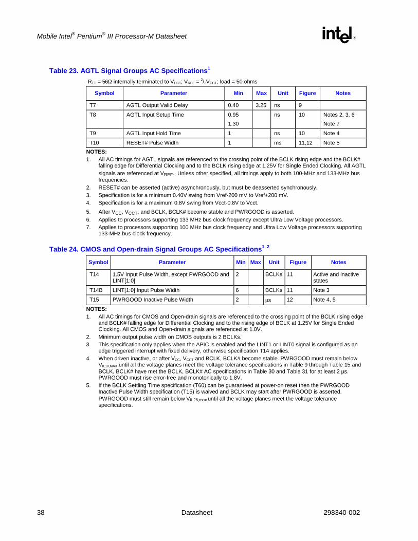
Mobile Intel® Pentium® III Processor-M Datasheet
38 Datasheet 298340-002
Table 23. AGTL Signal Groups AC Specifications1 RTT = 56Ω internally terminated to VCCT; VREF = 2/3VCCT; load = 50 ohms
Symbol Parameter Min Max Unit Figure Notes
T7 AGTL Output Valid Delay 0.40 3.25 ns 9
T8 AGTL Input Setup Time 0.95 1.30
ns 10 Notes 2, 3, 6 Note 7
T9 AGTL Input Hold Time 1 ns 10 Note 4
T10 RESET# Pulse Width 1 ms 11,12 Note 5 NOTES: 1. All AC timings for AGTL signals are referenced to the crossing point of the BCLK rising edge and the BCLK#
falling edge for Differential Clocking and to the BCLK rising edge at 1.25V for Single Ended Clocking. All AGTL signals are referenced at VREF. Unless other specified, all timings apply to both 100-MHz and 133-MHz bus frequencies.
2. RESET# can be asserted (active) asynchronously, but must be deasserted synchronously. 3. Specification is for a minimum 0.40V swing from Vref-200 mV to Vref+200 mV. 4. Specification is for a maximum 0.8V swing from Vcct-0.8V to Vcct. 5. After VCC, VCCT, and BCLK, BCLK# become stable and PWRGOOD is asserted. 6. Applies to processors supporting 133 MHz bus clock frequency except Ultra Low Voltage processors. 7. Applies to processors supporting 100 MHz bus clock frequency and Ultra Low Voltage processors supporting
133-MHz bus clock frequency.
Table 24. CMOS and Open-drain Signal Groups AC Specifications1, 2
Symbol Parameter Min Max Unit Figure Notes
T14 1.5V Input Pulse Width, except PWRGOOD and LINT[1:0]
2 BCLKs 11 Active and inactive states
T14B LINT[1:0] Input Pulse Width 6 BCLKs 11 Note 3
T15 PWRGOOD Inactive Pulse Width 2 µs 12 Note 4, 5 NOTES: 1. All AC timings for CMOS and Open-drain signals are referenced to the crossing point of the BCLK rising edge
and BCLK# falling edge for Differential Clocking and to the rising edge of BCLK at 1.25V for Single Ended Clocking. All CMOS and Open-drain signals are referenced at 1.0V.
2. Minimum output pulse width on CMOS outputs is 2 BCLKs. 3. This specification only applies when the APIC is enabled and the LINT1 or LINT0 signal is configured as an
edge triggered interrupt with fixed delivery, otherwise specification T14 applies. 4. When driven inactive, or after VCC, VCCT and BCLK, BCLK# become stable. PWRGOOD must remain below
VIL18,MAX until all the voltage planes meet the voltage tolerance specifications in Table 9 through Table 15 and BCLK, BCLK# have met the BCLK, BCLK# AC specifications in Table 30 and Table 31 for at least 2 µs. PWRGOOD must rise error-free and monotonically to 1.8V.
5. If the BCLK Settling Time specification (T60) can be guaranteed at power-on reset then the PWRGOOD Inactive Pulse Width specification (T15) is waived and BCLK may start after PWRGOOD is asserted. PWRGOOD must still remain below VIL25,max until all the voltage planes meet the voltage tolerance specifications.

Mobile Intel® Pentium ® III Processor-M Datasheet
298340-002 Datasheet 39
Table 25. Reset Configuration AC Specifications and Power On/Power Down Timings
Symbol Parameter Min Typ Max Unit Figure Notes
T16 Reset Configuration Signals (A[15:5]#, BREQ0#, FLUSH#, INIT#, PICD0) Setup Time
4 BCLKs 11
Before deassertion of RESET#
T17 Reset Configuration Signals (A[15:5]#, BREQ0#, FLUSH#, INIT#, PICD0) Hold Time
2 20 BCLKs 11 After clock that deasserts RESET#
T18 RESET#/PWRGOOD Setup Time 1 ms 12 Before deassertion of RESET# 1
T18A VCCT to VTTPWRGD Setup Time 1 ms 12
T18B VCC to PWRGOOD Setup Time 10 ms 12
T18C BSEL, VID valid time before VTTPWRGD assertion
1 µs 12
T18D RESET# inactive to Valid Outputs 1 BCLK 11
T18E RESET# inactive to Drive Signals 4 BCLKs 11
T19A Time from VCC(nominal)-12% to PWRGOOD low
0 ns 13 VCC(nominal) is the VID voltage setting
T19B All outputs valid after PWRGOOD low 0 ns 13
T19C All inputs required valid after PWRGOOD low 0 ns 13
T20A Time from VCCT-12% to VTTPWRGD low 0 ns 14
T20B All outputs valid after VTTPWRGD low 0 ns 14
T20C All inputs required valid after VTTPWRGD low 0 ns 14
T20D VID, BSEL signals valid after VTTPWRGD low
0 ns 14
NOTE: At least 1 ms must pass after PWRGOOD rises above VIH18min and BCLK, BCLK# meet their AC timing specification until RESET# may be deasserted.
Table 26. APIC Bus Signal AC Specifications 1
Symbol Parameter Min Max Unit Figure Notes
T21 PICCLK Frequency 2 33.3 MHz Note 2 T22 PICCLK Period 30 500 ns 6 T23 PICCLK High Time 10.5 ns 6 at>1.6V T24 PICCLK Low Time 10.5 ns 6 at<0.4V T25 PICCLK Rise Time 0.25 3.0 ns 6 (0.4V – 1.6V)
T26 PICCLK Fall Time 0.25 3.0 ns 6 (1.6V – 0.4V) T27 PICD[1:0] Setup Time 8.0 ns 9 Note 3 T28 PICD[1:0] Hold Time 2.5 ns 9 Note 3 T29 PICD[1:0] Valid Delay (Rising
Edge) PICD[1:0] Valid Delay (Falling Edge)
1.5 1.5
8.7 12.0
ns 8 Notes 3, 4
NOTES: 1. All AC timings for APIC signals are referenced to the PICCLK rising edge at 1.0V. All CMOS signals are
referenced at 1.0V. 2. The minimum frequency is 2 MHz when PICD0 is at 1.5V at reset Referenced to PICCLK Rising Edge. 3. For Open-drain signals, Valid Delay is synonymous with Float Delay. 4. Valid delay timings for these signals are specified into 150Ω to 1.5V and 0 pF of external load. For real system
timings these specifications must be derated for external capacitance at 105 ps/pF.

Mobile Intel® Pentium® III Processor-M Datasheet
40 Datasheet 298340-002
Table 27. TAP Signal AC Specifications1
Symbol Parameter Min Max Unit Figure Notes
T30 TCK Frequency — 16.67 MHz
T31 TCK Period 60 — ns 6
T32 TCK High Time 25.0 ns 6 ≥ VCMOSREF+0.2V, Note 2
T33 TCK Low Time 25.0 ns 6 ≤ VCMOSREF-0.2V, Note 2
T34 TCK Rise Time 5.0 ns 6 (VCMOSREF-0.2V) – (VCMOSREF+0.2V), Notes 2, 3
T35 TCK Fall Time 5.0 ns 6 (VCMOSREF+0.2V) – (VCMOSREF-0.2V) , Notes 2, 3
T36 TRST# Pulse Width 40.0 ns 16 Asynchronous, Note 2
T37 TDI, TMS Setup Time 5.0 ns 15 Note 4
T38 TDI, TMS Hold Time 14.0 ns 15 Note 4
T39 TDO Valid Delay 1.0 10.0 ns 15 Notes 5, 6
T40 TDO Float Delay 25.0 ns 15 Notes 2, 5, 6
T41 All Non-Test Outputs Valid Delay 2.0 25.0 ns 15 Notes 5, 7, 8
T42 All Non-Test Outputs Float Delay 25.0 ns 15 Notes 2, 5, 7, 8
T43 All Non-Test Inputs Setup Time 5.0 ns 15 Notes 4, 7, 8
T44 All Non-Test Inputs Hold Time 13.0 ns 15 Notes 4, 7, 8 NOTES: 1. All AC timings for TAP signals are referenced to the TCK rising edge at 1.0V. All TAP and CMOS signals are
referenced at 1.0V. 2. Not 100% tested. Specified by design/characterization. 3. 1 ns can be added to the maximum TCK rise and fall times for every 1 MHz below 16 MHz. 4. Referenced to TCK rising edge. 5. Referenced to TCK falling edge. 6. Valid delay timing for this signal is specified into 150Ω terminated to 1.5V and 0 pF of external load. For real
system timings these specifications must be derated for external capacitance at 105 ps/pF. 7. Non-Test Outputs and Inputs are the normal output or input signals (except TCK, TRST#, TDI, TDO, and TMS).
These timings correspond to the response of these signals due to boundary scan operations. 8. During Debug Port operation use the normal specified timings rather than the TAP signal timings.
Table 28. Quick Start/Deep Sleep AC Specifications1
Symbol Parameter Min Max Unit Figure Notes
T45 Quick Start Cycle Completion to Clock Stop or DPSLP# assertion
100 BCLKs 17, 18
T46 Quick Start Cycle Completion to Input Signals Stable 0 µs 17, 18
T47 Deep Sleep PLL Lock Latency 0 30 µs 17, 18 Note 2
T48 STPCLK# Hold Time from PLL Lock 0 ns 17, 18
T49 Input Signal Hold Time from STPCLK# Deassertion 8 BCLKs 17, 18 NOTES: 1. Input signals other than RESET# and BPRI# must be held constant in the Quick Start state. 2. The BCLK, BCLK# Settling Time specification (T60) applies to Deep Sleep state exit under all conditions.

Mobile Intel® Pentium ® III Processor-M Datasheet
298340-002 Datasheet 41
Table 29. Enhanced Intel SpeedStep Technology AC Specifications
Symbol Parameter Min Max Unit Figure Notes
T57 GHI# Setup Time from BCLK Restart or DPSLP# deassertion
150 ns 19 Note 1
T58 GHI# Hold Time from BCLK Restart or DPSLP# deassertion
30 µs 19 Note 1
T59 GHI# Sample Delay 10 µs 19 Note 1
T60 BCLK Settling Time 150 ns 19 Notes 2, 3 NOTES: 1. GHI# is ignored until 10 µs after BCLK, BCLK# stop or DPSLP# assertion, the setup and hold window must
occur after this time. 2. BCLK, BCLK# must meet the BCLK AC specification from within 150 ns of turning on (rising above VIL,BCLK). 3. This specification applies to the exit from the Deep Sleep state whether or not an Enhanced Intel SpeedStep
technology operating mode transition occurs.
Figure 6. BCLK (Single Ended)/PICCLK/TCK Generic Clock Timing Waveform
CLKVH
VLVTRIP
Th
Tl
Tp
Tr
Tf
D0003-01 NOTES:
Tr=T5S, T5S1, T34, T25 (Rise Time) Tf=T6S, T6S1, T35, T26 (Fall Time) Th=T3S, T3S1, T32, T23 (High Time) Tl=T4S, T4S1, T33, T24 (Low Time) Tp=T1S, T1S1, T31, T22 (Period) VTRIP=1.25V for BCLK (Single Ended);1.0V for PICCLK; 1.0V for TCK VL=0.5V for BCLK (Single Ended);0.4V for PICCLK; (VCMOSREF-0.2V) for TCK VH= 2.0V for BCLK (Single Ended);1.6V for PICCLK; (VCMOSREF+0.2V) for TCK
Figure 7. Differential BCLK/BCLK# Waveform (Common Mode)
BCLK
BCLK#
Vcross
V2,V3 (max)
V1,V3 (min)

Mobile Intel® Pentium® III Processor-M Datasheet
42 Datasheet 298340-002
Figure 8. BCLK/BCLK# Waveform (Differential Mode)
0V
T6 T5
T1
V4
V5
VIH_DIFF
VIl_DIFF
Figure 9. Valid Delay Timings
CLK
Signal
TXTx
TPW
V Valid Valid
D0004-00
Vc Vc
NOTES:
Tx = T7, T11, T29 (Valid Delay) Tpw = T14, T14B (Pulse Width) V = VREF for AGTL signal group; 1.0V for CMOS, Open-drain, APIC, and TAP signal groups Vc = Crossing point of BCLK rising edge and BCLK# falling edge for BCLK references (Differential Clock)
= 1.25V (Single Ended Clock)

Mobile Intel® Pentium ® III Processor-M Datasheet
298340-002 Datasheet 43
Figure 10. Setup and Hold Timings
CLK
SignalV Valid
ThTs
D0005-00
Vc
NOTES:
Ts = T8, T12, T27 (Setup Time) Th = T9, T13, T28 (Hold Time) V = VREF for AGTL signals; 1.0V for CMOS, APIC, and TAP signals Vc = Crossing point of BCLK rising edge and BCLK# falling edge for BCLK references (Differential Clock)
= 1.25V (Single Ended Clock)
Figure 11. Cold/Warm Reset and Configuration Timings
BCLK
RESET#
Tv
Tx
Tt
Tu
VC
V
D0006-02
Configuration(A[15:5], BREQ0#,
FLUSH#, INIT#,PICD0)
Tw
Valid
PICD[1:0]AGTL/non-AGTL
outputs
Non-configurationinputs
Ty
Valid
Tz
Active
NOTES:
Tt = T9 (AGTL Input Hold Time) Tu = T8 (AGTL Input Setup Time) Tv = T10 (RESET# Pulse Width) Tw= T16 (Reset Configuration Signals (A[15:5]#, BREQ0#, FLUSH#, INIT#, PICD0) Setup Time) Tx = T17 (Reset Configuration Signals (A[15:5]#, BREQ0#, FLUSH#, INIT#, PICD0) Hold Time)
Ty = T18D (RESET# inactive to Valid Outputs) Tz = T18E (RESET# inactive to Drive Signals) Vc= Crossing point of BCLK rising edge and BCLK# falling edge (Differential Clock)
= 1.25V (Single Ended Clock)

Mobile Intel® Pentium® III Processor-M Datasheet
44 Datasheet 298340-002
Figure 12. Power-on Sequence and Reset Timings
VCCT
Valid
VTTPWRGD
VID[4:0]/BSEL[1:0]
CMOSREF/CLKREF/VREF
PWRGOOD
RESET#
BCLK/BCLK#
VIH18,minVIL18,max
VIHVTTPWR,minVILVTTPWR,max
TaTc
Tb
VCC
V0040-00
Te
Td
NOTES:
Ta = T15 (PWRGOOD Inactive Pulse Width) Tb = T18 (RESET#/PWRGOOD Setup Time) Tc = T18B (Setup time from VCC valid until PWRGOOD assertion)
Td = T18A (Setup time from VCCT valid to VTTPWRGD assertion) Te = T18C(VID, BSEL valid time before VTTPWRGD assertion)

Mobile Intel® Pentium ® III Processor-M Datasheet
298340-002 Datasheet 45
Figure 13. Power Down Sequencing and Timings (VCC Leading)
VTTPWRGD
BCLK/BCLK#
V0044-00
VCCT, VREF
VCCMOS,CMOSREF,
CLKREF
VID[4:0]BSEL[1:0]
VCC
PICCLK
PWRGOOD
RESET#
PICD[1:0]
AGTL OUTPUTSOTHER CMOS OUTPUTS
ALL INPUTS
Ta
Tb
Tc
VCC-12%
VIL18
Valid
Valid
Valid
Valid
Valid
NOTES:
Ta = T19A (Time from VCC(nominal)-12% to PWRGOOD low) Tb = T19B (All outputs valid after PWRGOOD low) Tc = T19C (All inputs required valid after PWRGOOD low)
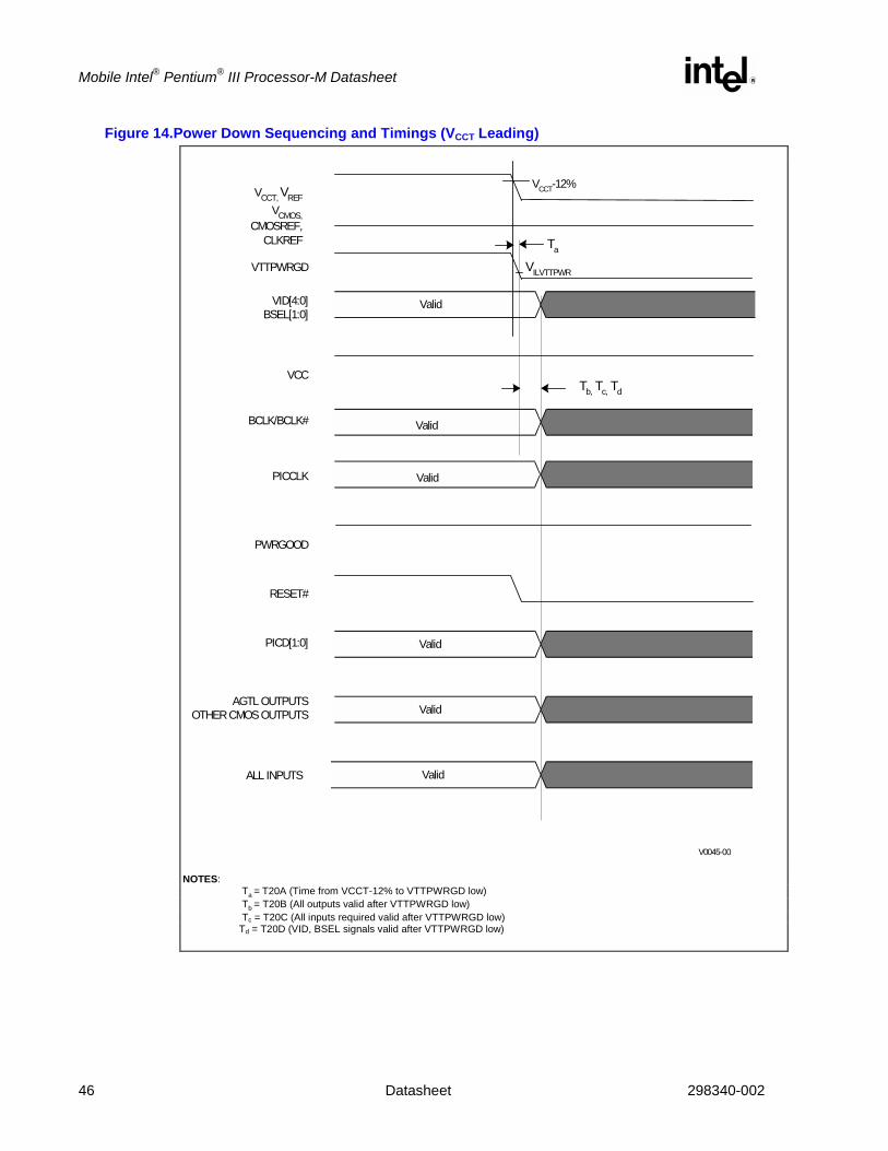
Mobile Intel® Pentium® III Processor-M Datasheet
46 Datasheet 298340-002
Figure 14.Power Down Sequencing and Timings (VCCT Leading)
VTTPWRGD
BCLK/BCLK#
V0045-00
VCCT, VREFVCMOS,
CMOSREF,CLKREF
VID[4:0]BSEL[1:0]
VCC
PICCLK
PWRGOOD
RESET#
PICD[1:0]
AGTL OUTPUTSOTHER CMOS OUTPUTS
ALL INPUTS
Ta
Tb, Tc, Td
VCCT-12%
VILVTTPWR
Valid
Valid
Valid
Valid
Valid
Valid
NOTES:
Ta = T20A (Time from VCCT-12% to VTTPWRGD low) Tb = T20B (All outputs valid after VTTPWRGD low) Tc = T20C (All inputs required valid after VTTPWRGD low)
Td = T20D (VID, BSEL signals valid after VTTPWRGD low)

Mobile Intel® Pentium ® III Processor-M Datasheet
298340-002 Datasheet 47
Figure 15.Test Timings (Boundary Scan)
TCK
TDI, TMS
InputSignals
TDO
OutputSignals
0.75V
Tv Tw
Tr Ts
Tx Tu
Ty Tz
D0008-01 NOTES:
Tr=T43 (All Non-Test Inputs Setup Time) Ts=T44 (All Non-Test Inputs Hold Time) Tu=T40 (TDO Float Delay) Tv=T37 (TDI, TMS Setup Time) Tw=T38 (TDI, TMS Hold Time) Tx=T39 (TDO Valid Delay) Ty=T41 (All Non-Test Outputs Valid Delay) Tz=T42 (All Non-Test Outputs Float Delay)
Figure 16. Test Reset Timings
TRST# 0.75V
TqD0009-01
NOTE: Tq=T36 (TRST# Pulse Width)
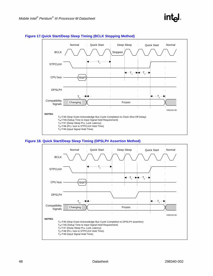
Mobile Intel® Pentium® III Processor-M Datasheet
48 Datasheet 298340-002
Figure 17.Quick Start/Deep Sleep Timing (BCLK Stopping Method)
Tw
stpgnt
StoppedBCLK
STPCLK#
CPU bus
DPSLP#
CompatibilitySignals Changing
Normal Quick Start Deep Sleep Quick Start Normal
Frozen
Tv
Ty
Tz
Tx
V00102-00
NOTES: Tv=T45 (Stop Grant Acknowledge Bus Cycle Completion to Clock Shut Off Delay) Tw=T46 (Setup Time to Input Signal Hold Requirement) Tx=T47 (Deep Sleep PLL Lock Latency) Ty=T48 (PLL lock to STPCLK# Hold Time) Tz=T49 (Input Signal Hold Time)
Figure 18. Quick Start/Deep Sleep Timing (DPSLP# Assertion Method)
Tw
stpgnt
BCLK
STPCLK#
CPU bus
DPSLP#
CompatibilitySignals Changing
Normal Quick Start Deep Sleep Quick Start Normal
Frozen
Tv
Ty
Tz
Tx
V00103-00
NOTES: Tv=T45 (Stop Grant Acknowledge Bus Cycle Completion to DPSLP# assertion) Tw=T46 (Setup Time to Input Signal Hold Requirement) Tx=T47 (Deep Sleep PLL Lock Latency) Ty=T48 (PLL lock to STPCLK# Hold Time) Tz=T49 (Input Signal Hold Time)

Mobile Intel® Pentium ® III Processor-M Datasheet
298340-002 Datasheet 49
Figure 19. Enhanced Intel SpeedStep Technology/Deep Sleep Timing
BCLK V ILBCLK
BCLK off or DPSLP# asserted
BCLK on and DPSLP# de-asserted (out of spec)
BCLK on(in spec)
Vc
BCLK on
T s
V0036-00
GHI#
T h T yT x
Vc
Vghi
NOTES:
Ts=T57 (GHI# Setup Time from BCLK Restart) Th=T58 (GHI# Hold Time from BCLK Restart) Tx=T59 (GHI# Sample Delay) Ty=T60 (BCLK Settling Time) Vc = Crossing point of BCLK rising edge and BCLK# falling edge (Differential Clocking)
= 1.25V (Single Ended Clocking) Vghi = GHI# reference voltage = VCCT /2

Mobile Intel® Pentium® III Processor-M Datasheet
50 Datasheet 298340-002
4. System Signal Simulations Systems must be simulated using IBIS models to determine if they are compliant with this specification. All references to BCLK signal quality also apply to BCLK# for Differential Clocking.
4.1 System Bus Clock (BCLK) and PICCLK DC Specifications and AC Signal Quality Specifications
Table 30. BCLK (Differential) DC Specifications and AC Signal Quality Specifications
Symbol Parameter Min Max Unit Figure Notes
V1 VIL,BCLK -0.2 0.35 V 7 Note 1
V2 VIH,BCLK 0.92 1.45 V 7 Note 1
V3 VIN Absolute Voltage Range -0.2 1.45 V 7 Undershoot/Overshoot, Note 2
V4 BCLK Rising Edge Ringback
0.35 V 8 Note 3
V5 BCLK Falling Edge Ringback
-0.35 V 8 Note 3
VBCLK_DPSLP BCLK Voltage in Deep Sleep State
0.4 1.45 V Note 4
VBCLK#_DPSLP BCLK# Voltage in Deep Sleep State
0 VBCLK_DPSLP
- 0.2V V Note 4
NOTES: 1. The clock must rise/fall monotonically between VIL,BCLK and VIH,BCLK . 2. These specifications apply only when BCLK, BCLK# are running. 3. The rising and falling edge ringback voltage specified is the minimum (rising) or maximum (falling) voltage the
differential waveform can go to after passing the VIH_DIFF (rising) or VIL_DIFF (falling) levels. VIL_DIFF (max) = -0.57V, VIH_DIFF (min) = 0.57V.
4. Applies when BCLK and BCLK# are stopped in Deep Sleep State.
Table 31. BCLK (Single Ended) DC Specifications and AC Signal Quality Specifications
Symbol Parameter Min Max Unit Figure Notes
V1 VIL,BCLK 0.3 V 20 Note 1
V2 VIH,BCLK 2.2 V 20 Note 1
V3 VIN Absolute Voltage Range -0.5 3.1 V 20 Undershoot/Overshoot, Note 2
V4 BCLK Rising Edge Ringback 2.0 V 20 Absolute Value, Note 3
V5 BCLK Falling Edge Ringback 0.5 V 20 Absolute Value, Note 3 NOTES: 1. The clock must rise/fall monotonically between VIL,BCLK and VIH,BCLK . BCLK must be stopped in the low state. 2. These specifications apply only when BCLK is running. BCLK may not be above VIH,BCLK,max or below VIL,BCLK,min
for more than 50% of the clock cycle. 3. The rising and falling edge ringback voltage specified is the minimum (rising) or maximum (falling) absolute
voltage the BCLK signal can go to after passing the VIH,BCLK (rising) or VIL,BCLK (falling) voltage limits.

Mobile Intel® Pentium ® III Processor-M Datasheet
298340-002 Datasheet 51
Table 32. PICCLK DC Specifications and AC Signal Quality Specifications
Symbol Parameter Min Max Unit Figure Notes
V1 VIL20 0.4 V 20 Note 1
V2 VIH20 1.6 V 20 Note 1
V3 VIN Absolute Voltage Range -0.5 2.4 V 20 Undershoot, Overshoot, Note 2
V4 PICCLK Rising Edge Ringback 1.6 V 20 Absolute Value, Note 3
V5 PICCLK Falling Edge Ringback 0.4 V 20 Absolute Value, Note 3 NOTES: 1. The clock must rise/fall monotonically between VIL20 and VIH20. 2. These specifications apply only when PICCLK is running. See the DC specifications for when PICCLK is
stopped. PICCLK may not be above VIH20,max or below VIL20,min for more than 50% of the clock cycle. 3. The rising and falling edge ringback voltage specified is the minimum (rising) or maximum (falling) absolute
voltage the PICCLK signal can go to after passing the VIH20 (rising) or VIL20 (falling) voltage limits.
Figure 20. BCLK (Single Ended)/PICCLK Generic Clock Waveform
V0012-01
V1
V2
V3max
V4
V3min
V5

Mobile Intel® Pentium® III Processor-M Datasheet
52 Datasheet 298340-002
4.2 AGTL AC Signal Quality Specifications Ringback specifications for the AGTL signals are as follows:
Ringback below VREF,max + 200 mV is not authorized during low to high transitions. Ringback above VREF,min – 200 mV is not authorized during high to low transitions. Overshoot and undershoot specifications are documented in Table 33 and Table 34 and illustrated in Figure 21.
Figure 21. Maximum Acceptable Overshoot/Undershoot Waveform
Max
Vss
Time dependant Overshoot
Time dependant Undershoot
Min

Mobile Intel® Pentium ® III Processor-M Datasheet
298340-002 Datasheet 53
Table 33. 133-MHz AGTL Signal Group Overshoot/Undershoot Tolerance at the Processor Core
Allowed Pulse Duration (ns) [Tj=100C] Max VCCT + Overshoot/Undershoot
Magnitude (volts) Activity Factor = 0.01 Activity Factor = 0.1 Activity Factor = 1
1.78 1.5 0.15 0.015
1.73 3.5 0.35 0.035
1.68 7.2 0.72 0.072
1.63 15 1.5 0.15
1.58 15 3.2 0.32
1.53 15 6.5 0.65
1.48 15 14 1.40 NOTES: 1. Under no circumstances should the sum of the Max VCCT and absolute value of the Overshoot/Undershoot
voltage exceed 1.78V. 2. Activity factor of 1 represents the same toggle rate as the 133-MHz clock. 3. Ringbacks below VCCT cannot be subtracted from overshoots. Lesser undershoot does not allocate longer or
larger overshoot. 4. Ringbacks above ground cannot be subtracted from undershoots. Lesser overshoot does not allocate longer or
larger undershoot. 5. System designers are encouraged to follow Intel provided AGTL layout guidelines. 6. All values are specified by design characterization and are not tested.
Table 34. 100-MHz AGTL Signal Group Overshoot/Undershoot Tolerance at the Processor Core
Allowed Pulse Duration (ns) [Tj=100C] Max VCCT + Overshoot/Undershoot
Magnitude (volts) Activity Factor = 0.01 Activity Factor = 0.1 Activity Factor = 1
1.78 1.6 0.16 0.016
1.73 4.5 0.45 0.045
1.68 9.5 0.95 0.095
1.63 20 2.0 0.2
1.58 20 4.2 0.42
1.53 20 8.5 0.85
1.48 20 19 1.9
NOTES: 1. Under no circumstances should the sum of the Max VCCT and absolute value of the Overshoot/Undershoot
voltage exceed 1.78V. 2. Activity factor of 1 represents the same toggle rate as the 100-MHz clock. 3. Ringbacks below VCCT cannot be subtracted from overshoots. Lesser undershoot does not allocate longer or
larger overshoot. 4. Ringbacks above ground cannot be subtracted from undershoots. Lesser overshoot does not allocate longer or
larger undershoot. 5. System designers are encouraged to follow Intel provided AGTL layout guidelines. 6. All values are specified by design characterization and are not tested.

Mobile Intel® Pentium® III Processor-M Datasheet
54 Datasheet 298340-002
4.3 Non-AGTL Signal Quality Specifications Signals driven to the Mobile Intel Pentium III Processor-M should meet signal quality specifications to ensure that the processor reads data properly and that incoming signals do not affect the long-term reliability of the processor. The overshoot and undershoot specifications for non AGTL signals are shown in Table 35. Ringback must not exceed the CMOS VIH and VIL specification levels in Table 18.
Table 35. Non-AGTL Signal Group Overshoot/Undershoot Tolerance at the Processor Core
Allowed Pulse Duration (ns) [Tj=100C] Max VCmos + Overshoot/Undershoot
Magnitude (volts) Activity Factor = 0.01 Activity Factor = 0.1 Activity Factor = 1
2.38 6.5 0.65 0.065
2.33 13 1.3 0.13
2.28 29 2.9 0.29
2.23 60 6 0.6
2.18 60 12 1.2
2.13 60 26 2.6
2.08 60 56 5.6 NOTES: 1. VCMOS(nominal) = 1.5V. 2. Under no circumstances should the sum of the Max VCMOS and absolute value of the Overshoot/Undershoot
voltage exceed 2.38V. 3. Activity factor of 1 represents a toggle rate of 33 MHz. 4. System designers are encouraged to follow Intel provided non-AGTL layout guidelines. 5. All values are specified by design characterization, and are not tested.
4.3.1 PWRGOOD, VTTPWRGD Signal Quality Specifications The processor requires PWRGOOD to be a clean indication that clocks and the power supplies (VCC, VCCT, etc.) are stable and within their specifications. Clean implies that the signal will remain below VIL18 and without errors from the time that the power supplies are turned on, until they come within specification. The signal will then transition monotonically to a high (1.8V) state. The VTTPWRGD signal must also transition monotonically.

Mobile Intel® Pentium ® III Processor-M Datasheet
298340-002 Datasheet 55
5. Mechanical Specifications
5.1 Socketable Micro-FCPGA Package The Mobile Intel Pentium III Processor-M is packaged in a 478-pin Micro-FCPGA package. The Low Voltage and Ultra Low Voltage processors will not be available in this package. The mechanical specifications for the socketable package are provided in Table 36. Figure 22 through Figure 24 illustrate different views of the package.
Table 36. Socketable Micro-FCPGA Package Specification
Symbol Parameter Min Max Unit
A Overall height, top of die to package seating plane 1.81 2.03 mm - Overall height, top of die to PCB surface, including socket(1) 4.69 5.15 mm A1 Pin length 1.95 2.11 mm A2 Die height 0.854 mm
A3 Pin-side capacitor height - 1.25 mm B Pin diameter 0.28 0.36 mm D Package substrate length 34.9 35.1 mm E Package substrate width 34.9 35.1 mm D1 Die length 11.18 mm E1 Die width 7.19 mm
e Pin pitch 1.27 mm K Package edge keep-out 5 mm K1 Package corner keep-out 7 mm K3 Pin-side capacitor boundary 14 mm - Pin tip radial true position <=0.254 mm N Pin count 478 each
Pdie Allowable pressure on the die for thermal solution - 689 kPa W Package weight 4.5 g
Package Surface Flatness 0.286 mm NOTES: 1. All dimensions are subject to change. 2. Overall height with socket is based on design dimensions of the Micro-FCPGA package and socket with no
thermal solution attached. Values were based on design specifications and tolerances. This dimension is subject to change based on socket design, OEM motherboard design, or OEM SMT process.

Mobile Intel® Pentium® III Processor-M Datasheet
56 Datasheet 298340-002
Figure 22. Socketable Micro-FCPGA Package - Top and Bottom Isometric Views
TOP VIEW BOTTOM VIEW
LABEL
PACKAGE KEEPOUT
DIE
CAPACITOR AREA
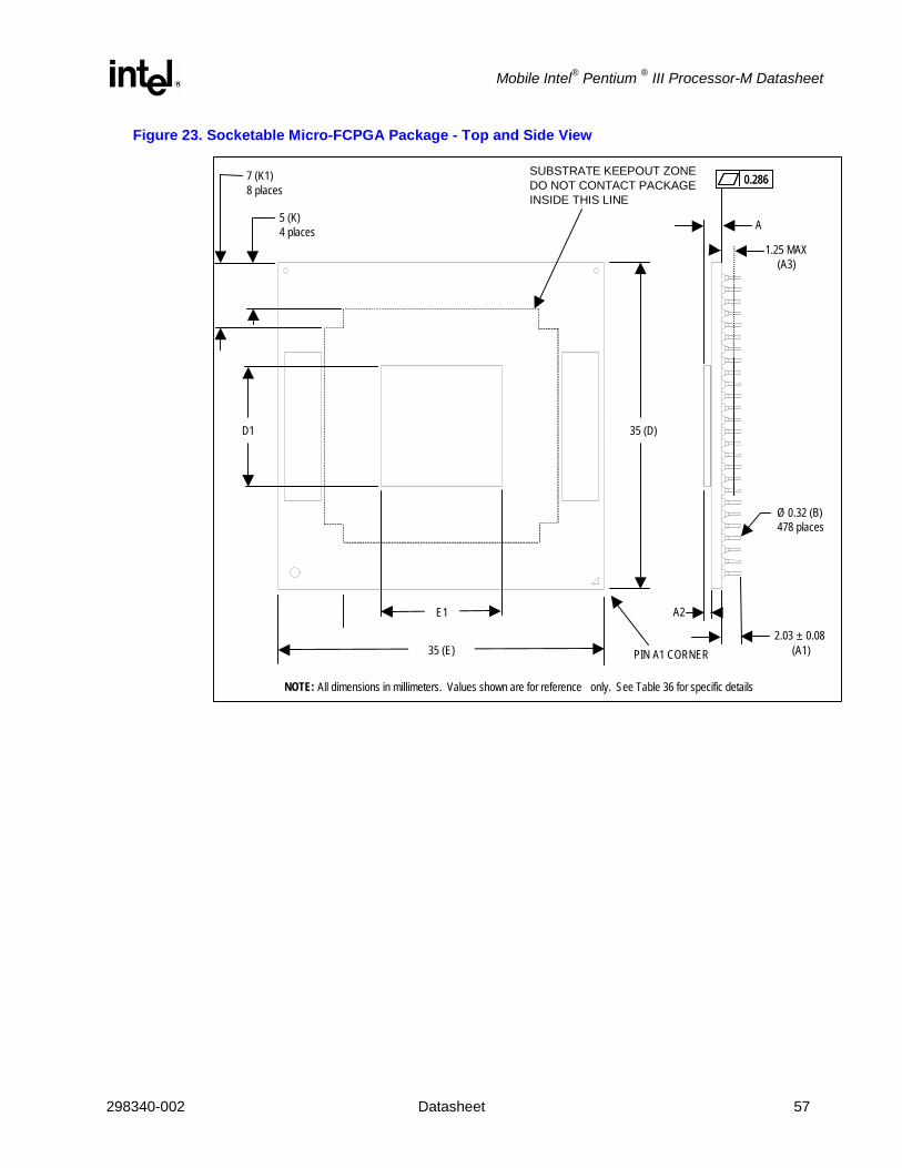
Mobile Intel® Pentium ® III Processor-M Datasheet
298340-002 Datasheet 57
Figure 23. Socketable Micro-FCPGA Package - Top and Side View
35 (E)
35 (D)
PIN A1 CORNER
E1
D1
A 1.25 MAX
(A3)
Ø 0.32 (B)478 places
2.03 ± 0.08 (A1)
A2
SUBSTRATE KEEPOUT ZONE DO NOT CONTACT PACKAGE INSIDE THIS LINE
7 (K1) 8 places
5 (K) 4 places
NOTE: All dimensions in millimeters. Values shown are for reference only. See Table 36 for specific details
0.2860.286

Mobile Intel® Pentium® III Processor-M Datasheet
58 Datasheet 298340-002
Figure 24. Socketable Micro-FCPGA Package - Bottom View
1 2
3 4 6 8 10 12 14 16 18 20 22 24 26
5 7 9 11 13 15 17 19 21 23 25
A B
C E
D F
G H
J K
L M
N P
R T
U V
W Y
AA AB
AC AD
AE AF
NOTE : All dimensions in millimeters. Values shown are for reference only. See Table 36 for specific details.
25X 1.27 (e)
25X 1.27 (e)
14 (K3)
14 (K3)

Mobile Intel® Pentium ® III Processor-M Datasheet
298340-002 Datasheet 59
5.2 Surface Mount Micro-FCBGA Package The Mobile Intel Pentium III Processor-M will also be available in a surface mount, 479-ball Micro-FCBGA package. The Low Voltage and Ultra Low Voltage processors will be available only in this package. Mechanical specifications are shown in Table 37. Figure 25 through Figure 27 illustrate different views of the package.
The Micro-FCBGA package may have capacitors placed in the area surrounding the die. Since the die-side capacitors are electrically conductive, and only slightly shorter than the die height, care should be taken to avoid contacting the capacitors with electrically conductive materials. Doing so may short the capacitors, and possibly damage the device or render it inactive. The use of an insulating material between the capacitors and any thermal solution should be considered to prevent capacitor shorting.
Table 37. Micro-FCBGA Package Mechanical Specifications
Symbol Parameter Min Max Unit
A Overall height, as delivered (1) 2.27 2.77 mm A2 Die height 0.854 mm b Ball diameter 0.78 mm D Package substrate length 34.9 35.1 mm E Package substrate width 34.9 35.1 mm D1 Die length 11.18 mm
E1 Die width 7.19 mm e Ball pitch 1.27 mm N Ball count 479 each K Keep-out outline from edge of package 5 mm K1 Keep-out outline at corner of package 7 mm K2 Capacitor keep-out height - 0.7 mm
S Package edge to first ball center 1.625 mm -- Solder ball coplanarity 0.20 mm Pdie Allowable pressure on the die for thermal solution - 689 kPa W Package weight 4.5 g NOTES: 1. All dimensions are subject to change. 2. Overall height as delivered. Values were based on design specifications and tolerances. Final height after
surface mount depends on OEM motherboard design and SMT process.
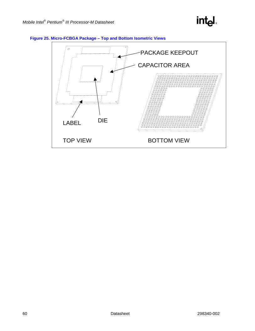
Mobile Intel® Pentium® III Processor-M Datasheet
60 Datasheet 298340-002
Figure 25. Micro-FCBGA Package – Top and Bottom Isometric Views
TOP VIEW BOTTOM VIEW
LABEL DIE
PACKAGE KEEPOUT
CAPACITOR AREA

Mobile Intel® Pentium ® III Processor-M Datasheet
298340-002 Datasheet 61
Figure 26. Micro-FCBGA Package – Top and Side Views
35 (E)
35 (D)
PIN A1 CORNER
E1
D1
A
Ø 0.78 (b)479 places
K2
SUBSTRATE KEEPOUT ZONE DO NOT CONTACT PACKAGE INSIDE THIS LINE
7 (K1) 8 places
5 (K)4 places
NOTE: All dimensions in millimeters. Values shown are for reference only. See Table 37 for specific details
A2
0.20

Mobile Intel® Pentium® III Processor-M Datasheet
62 Datasheet 298340-002
Figure 27. Micro-FCBGA Package - Bottom View
1 2
34 6 8 10 12 14 16 18 20 22 24 26
5 7 9 11 13 15 17 19 21 23 25
AB
C E
D F
GH
J K
L M
N P
R T
UV
W Y
AA AB
AC AD
AE AF
NOTE : All dimensions in millimeters. Values shown are for reference only. See Table 37 for specific details.
25X 1.27 (e)
25X 1.27 (e)
1.625 (S)4 places
1.625 (S)4 places

Mobile Intel® Pentium ® III Processor-M Datasheet
298340-002 Datasheet 63
5.3 Signal Listings Figure 28 is a top-side view of the ball or pin map of the Mobile Intel Pentium III Processor-M with the voltage balls/pins called out. Table 38 lists the signals in ball/pin number order. Table 39 lists the signals in signal name order.
Figure 28. Pin/Ball Map - Top View
A10# VREF NC A31# BREQ0# A23# A27# A24# NC A35# A26# A33# A32# D0# D2# D15# D9# D7# VREF D8# D10# D11# VSS VCCT
NC VSS A25# VSS A17# VSS A21# VSS A20# VSS A18# VSS A34# VSS RESET# VSS D1# VSS D4# VSS D17# VSS D18# D14# D24# VSS
NC A16# A28# NC VCCT A19# VCCT A22# VCCT A30# VCCT A29# VCCT BERR# VCCT D6# VCCT D12# VCCT D5# VCCT NC VSS D20# VSS D30#
NC VSS A13# VSS VCCT VCC VSS VCC VSS VCC VSS VCC VSS VCC VSS VCC VSS VCC VSS VCC VSS VCC D3# D13# D22# NC
NC TESTHI VCCT VCC VCCT VCC VSS VCC VSS VCC VSS VCC VSS VCC VSS VCC VSS VCC VSS VCC VSS D16# D23# VSS D19#
NC VSS A14# VSS VSS VCC VSS VCC VSS VCC VSS VCC VSS VCC VSS VCC VSS VCC VSS VCC VSS VCC VSS D21# D36# D27#
A9# A5# A15# VCCT VCC VSS VCC VSS VCCT D25# VSS D32#
A12# VSS A8# VSS VSS VCC VSS VCC VSS D26# D29# VREF
A4# A7# A11# VCCT VCC VSS VCC VSS VCCT D34# VSS D38#
A3# VSS A6# VSS VSS VCC VSS VCC VSS D31# D33# D35#
REQ4# BNR# REQ1# VCCT GHI# VSS VCC VSS VCCT D28# VSS D42#
VSS VSS VSS RSP# VCC VSS VCC VSS D39# D45# D48#
VREF PLL2 PLL1 NC VCC VSS VCC VSS VCCT NC VSS D37#
NC VSS API# NC NC VCC VSS VCC VSS D49# D41# NC
REQ0# BPRI# VID4 VSS VCC VSS VCC VSS VCCT D43# VSS D44#
REQ2# VSS DEFER# RP# VSS VCC VSS VCC VSS D47# D57# D51#
REQ3# HITM# RS2# VSS VCC VSS VCC VSS VCCT D52# VSS D40#
RS1# VSS LOCK# VCCT VSS VCC VSS VCC VSS D63# D46# D55#
TRDY# AERR# DBSY# VSS VCC VSS VCC VSS VCCT D59# VSS D54#
DRDY# VSS RS0# VSS VCC VSS VCC VSS D58# D53# D60#
VREF HIT# ADS# VCCT VCC VSS VCC VSS VCC VSS VCC VSS VCC VSS VCC VSS VCC VSS VCC VSS VCC VSS VCCT D62# VSS D50#
VID0 VSS AP0# PWRGOOD
VSS VCC VSS VCC VSS VCC VSS VCC VSS VCC VSS VCC VSS VCC VSS VCC VSS VCC VSS D61# D56# VREF
BCLK VID1 A20M# VCCT VCC VSS VCC VSS VCC VSS VCC VSS VCC VSS VCC VSS VCC VSS VCC VSS VCC VSS VCCT DEP3# VSS DEP6#
BCLK# /CLKREF VSS SMI# NC CMOS
REFVCCT TDI VCCT IGNNE# TCK TDO VCCT NC VCCT LINT0 NCTRL PICD1 VCCT PICD0 VCCT BPM1# BPM0# NC DEP7# DEP1# DEP5#
VSS VID2 VCCT STPCLK# VSS INIT# VSS NC VSS NC VSS BSEL0 VSS LINT1 VSS RTTIMPEDP
VSS VCCT VSS BP3# VSS PRDY# VSS DEP0# DEP2# VSS
VCCT VCCT VID3 IERR# FLUSH# FERR# TMS DPSLP# VREF BSEL1 TESTHI CMOSREF
THRMDATHRMDC TRST# EDGECTRLP
NC NC PREQ# PICCLK VREF BP2# BINIT# DEP4# VSS VSS
A
B
C
D
E
F
G
H
J
K
L
M
N
P
R
T
U
V
W
Y
AA
AB
AC
AD
AE
AF
1 2 3 4 5 6 7 8 9 10 11 12 13 14 15 16 17 18 19 20 21 22 23 24 25 26
VTTPWRGD
A
B
C
D
E
F
G
H
J
K
L
M
N
P
R
T
U
V
W
Y
AA
AB
AC
AD
AE
AF
1 2 3 4 5 6 7 8 9 10 11 12 13 14 15 16 17 18 19 20 21 22 23 24 25 26
VCC VSS OtherVCCT
TESTLO
TESTLO
NC
Note : A2 pin is de-populated on Micro-FCPGA package

Mobile Intel® Pentium® III Processor-M Datasheet
64 Datasheet 298340-002
Table 38. Signal Listing in Order by Pin/Ball Number
No. Signal Name No. Signal Name No. Signal Name No. Signal Name
A3 A10# B18 VSS D7 VSS E22 VSS
A4 VREF B19 D4# D8 VCC E23 D16#
A5 NC B20 VSS D9 VSS E24 D23#
A6 A31# B21 D17# D10 VCC E25 VSS
A7 BREQ0# B22 VSS D11 VSS E26 D19#
A8 A23# B23 D18# D12 VCC F1 NC
A9 A27# B24 D14# D13 VSS F2 VSS
A10 A24# B25 D24# D14 VCC F3 A14#
A11 NC B26 VSS D15 VSS F4 VSS
A12 A35# C1 NC D16 VCC F5 VSS
A13 A26# C2 A16# D17 VSS F6 VCC
A14 A33# C3 A28# D18 VCC F7 VSS
A15 A32# C4 NC D19 VSS F8 VCC
A16 D0# C5 VCCT D20 VCC F9 VSS
A17 D2# C6 A19# D21 VSS F10 VCC
A18 D15# C7 VCCT D22 VCC F11 VSS
A19 D9# C8 A22# D23 D3# F12 VCC
A20 D7# C9 VCCT D24 D13# F13 VSS
A21 VREF C10 A30# D25 D22# F14 VCC
A22 D8# C11 VCCT D26 NC F15 VSS
A23 D10# C12 A29# E1 NC F16 VCC
A24 D11# C13 VCCT E2 TESTHI F17 VSS
A25 VSS C14 BERR# E3 VTTPWRGD F18 VCC
A26 VCCT C15 VCCT E4 VCCT F19 VSS
B1 NC C16 D6# E5 VCC F20 VCC
B2 VSS C17 VCCT E6 VCCT F21 VSS
B3 A25# C18 D12# E7 VCC F22 VCC
B4 VSS C19 VCCT E8 VSS F23 VSS
B5 A17# C20 D5# E9 VCC F24 D21#
B6 VSS C21 VCCT E10 VSS F25 D36#
B7 A21# C22 NC E11 VCC F26 D27#
B8 VSS C23 VSS E12 VSS G1 A9#
B9 A20# C24 D20# E13 VCC G2 A5#
B10 VSS C25 VSS E14 VSS G3 A15#
B11 A18# C26 D30# E15 VCC G4 VCCT
B12 VSS D1 NC E16 VSS G5 VCC
B13 A34# D2 VSS E17 VCC G6 VSS
B14 VSS D3 A13# E18 VSS G21 VCC
B15 RESET# D4 VSS E19 VCC G22 VSS
B16 VSS D5 VCCT E20 VSS G23 VCCT
B17 D1# D6 VCC E21 VCC G24 D25#

Mobile Intel® Pentium ® III Processor-M Datasheet
298340-002 Datasheet 65
No. Signal Name No. Signal Name No. Signal Name No. Signal Name
G25 VSS L4 VCCT P23 VSS V2 VSS
G26 D32# L5 GHI# P24 D49# V3 LOCK#
H1 A12# L6 VSS P25 D41# V4 VCCT
H2 VSS L21 VCC P26 NC V5 VSS
H3 A8# L22 VSS R1 REQ0# V6 VCC
H4 VSS L23 VCCT R2 BPRI# V21 VSS
H5 VSS L24 D28# R3 VID4 V22 VCC
H6 VCC L25 VSS R4 VSS V23 VSS
H21 VSS L26 D42# R5 VCC V24 D63#
H22 VCC M1 TESTLO R6 VSS V25 D46#
H23 VSS M2 VSS R21 VCC V26 D55#
H24 D26# M3 VSS R22 VSS W1 TRDY#
H25 D29# M4 VSS R23 VCCT W2 AERR#
H26 VREF M5 RSP# R24 D43# W3 DBSY#
J1 A4# M6 VCC R25 VSS W4 VSS
J2 A7# M21 VSS R26 D44# W5 VCC
J3 A11# M22 VCC T1 REQ2# W6 VSS
J4 VCCT M23 VSS T2 VSS W21 VCC
J5 VCC M24 D39# T3 DEFER# W22 VSS
J6 VSS M25 D45# T4 RP# W23 VCCT
J21 VCC M26 D48# T5 VSS W24 D59#
J22 VSS N1 VREF T6 VCC W25 VSS
J23 VCCT N2 PLL2 T21 VSS W26 D54#
J24 D34# N3 PLL1 T22 VCC Y1 DRDY#
J25 VSS N4 NC T23 VSS Y2 VSS
J26 D38# N5 VCC T24 D47# Y3 RS0#
K1 A3# N6 VSS T25 D57# Y4 TESTLO
K2 VSS N21 VCC T26 D51# Y5 VSS
K3 A6# N22 VSS U1 REQ3# Y6 VCC
K4 VSS N23 VCCT U2 HITM# Y21 VSS
K5 VSS N24 NC U3 RS2# Y22 VCC
K6 VCC N25 VSS U4 VSS Y23 VSS
K21 VSS N26 D37# U5 VCC Y24 D58#
K22 VCC P1 NC U6 VSS Y25 D53#
K23 VSS P2 VSS U21 VCC Y26 D60#
K24 D31# P3 API# U22 VSS AA1 VREF
K25 D33# P4 NC U23 VCCT AA2 HIT#
K26 D35# P5 NC U24 D52# AA3 ADS#
L1 REQ4# P6 VCC U25 VSS AA4 VCCT
L2 BNR# P21 VSS U26 D40# AA5 VCC
L3 REQ1# P22 VCC V1 RS1# AA6 VSS

Mobile Intel® Pentium® III Processor-M Datasheet
66 Datasheet 298340-002
No. Signal Name No. Signal Name No. Signal Name No. Signal Name
AA7 VCC AB22 VCC AD11 TDO AE26 VSS
AA8 VSS AB23 VSS AD12 VCCT AF1 VCCT
AA9 VCC AB24 D61# AD13 NC AF2 VCCT
AA10 VSS AB25 D56# AD14 VCCT AF3 VID3
AA11 VCC AB26 VREF AD15 LINT0 AF4 IERR#
AA12 VSS AC1 BCLK AD16 NCTRL AF5 FLUSH#
AA13 VCC AC2 VID1 AD17 PICD1 AF6 FERR#
AA14 VSS AC3 A20M# AD18 VCCT AF7 TMS
AA15 VCC AC4 VCCT AD19 PICD0 AF8 DPSLP#
AA16 VSS AC5 VCC AD20 VCCT AF9 VREF
AA17 VCC AC6 VSS AD21 BPM1# AF10 BSEL1
AA18 VSS AC7 VCC AD22 BPM0# AF11 TESTHI
AA19 VCC AC8 VSS AD23 NC AF12 CMOSREF
AA20 VSS AC9 VCC AD24 DEP7# AF13 THRMDA
AA21 VCC AC10 VSS AD25 DEP1# AF14 THRMDC
AA22 VSS AC11 VCC AD26 DEP5# AF15 TRST#
AA23 VCCT AC12 VSS AE1 VSS AF16 EDGECTRLP
AA24 D62# AC13 VCC AE2 VID2 AF17 NC
AA25 VSS AC14 VSS AE3 VCCT AF18 NC
AA26 D50# AC15 VCC AE4 STPCLK# AF19 PREQ#
AB1 VID0 AC16 VSS AE5 VSS AF20 PICCLK
AB2 VSS AC17 VCC AE6 INIT# AF21 VREF
AB3 AP0# AC18 VSS AE7 VSS AF22 BP2#
AB4 PWRGOOD AC19 VCC AE8 NC AF23 BINIT#
AB5 VSS AC20 VSS AE9 VSS AF24 DEP4#
AB6 VCC AC21 VCC AE10 NC AF25 VSS
AB7 VSS AC22 VSS AE11 VSS AF26 VSS
AB8 VCC AC23 VCCT AE12 BSEL0
AB9 VSS AC24 DEP3# AE13 VSS
AB10 VCC AC25 VSS AE14 LINT1
AB11 VSS AC26 DEP6# AE15 VSS
AB12 VCC AD1 BCLK#/CLKREF AE16 RTTIMPEDP
AB13 VSS AD2 VSS AE17 VSS
AB14 VCC AD3 SMI# AE18 VCCT
AB15 VSS AD4 NC AE19 VSS
AB16 VCC AD5 CMOSREF AE20 BP3#
AB17 VSS AD6 VCCT AE21 VSS
AB18 VCC AD7 TDI AE22 PRDY#
AB19 VSS AD8 VCCT AE23 VSS
AB20 VCC AD9 IGNNE# AE24 DEP0#
AB21 VSS AD10 TCK AE25 DEP2#
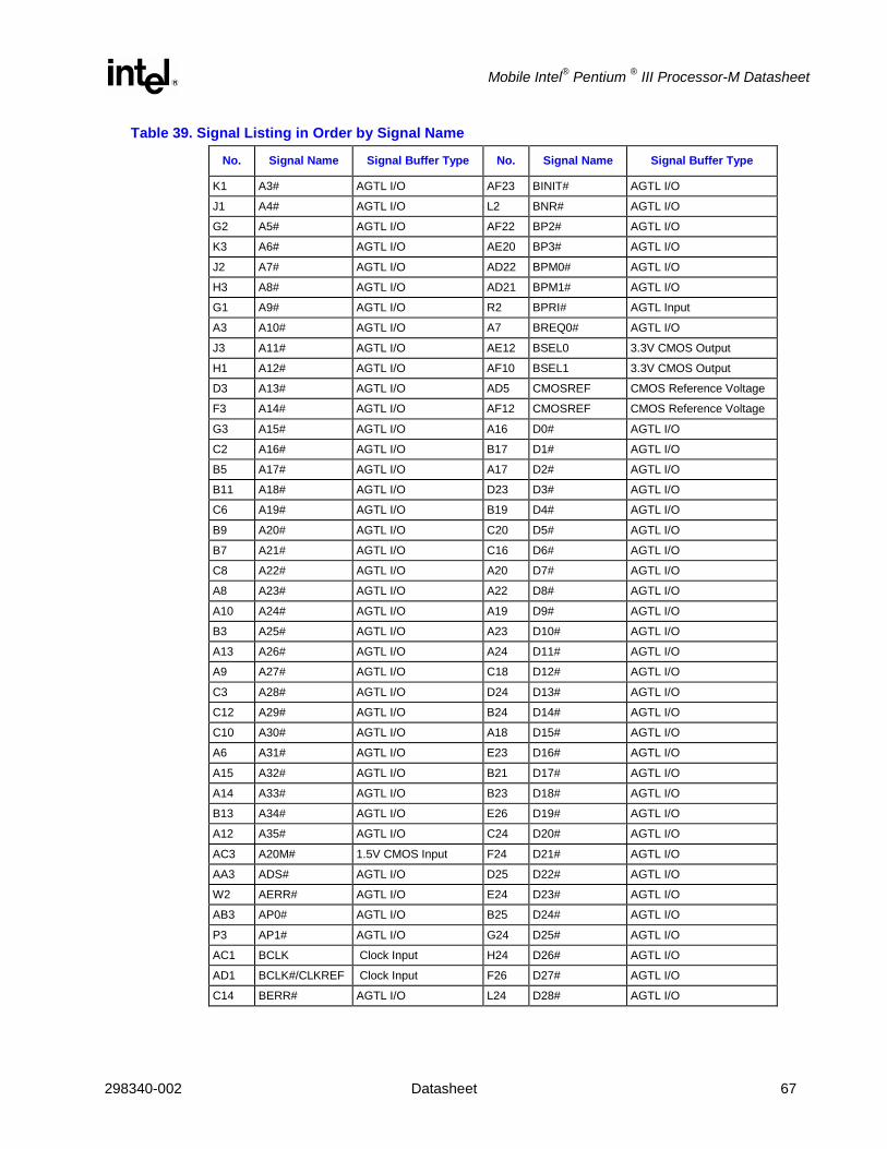
Mobile Intel® Pentium ® III Processor-M Datasheet
298340-002 Datasheet 67
Table 39. Signal Listing in Order by Signal Name
No. Signal Name Signal Buffer Type No. Signal Name Signal Buffer Type
K1 A3# AGTL I/O AF23 BINIT# AGTL I/O
J1 A4# AGTL I/O L2 BNR# AGTL I/O
G2 A5# AGTL I/O AF22 BP2# AGTL I/O
K3 A6# AGTL I/O AE20 BP3# AGTL I/O
J2 A7# AGTL I/O AD22 BPM0# AGTL I/O
H3 A8# AGTL I/O AD21 BPM1# AGTL I/O
G1 A9# AGTL I/O R2 BPRI# AGTL Input
A3 A10# AGTL I/O A7 BREQ0# AGTL I/O
J3 A11# AGTL I/O AE12 BSEL0 3.3V CMOS Output
H1 A12# AGTL I/O AF10 BSEL1 3.3V CMOS Output
D3 A13# AGTL I/O AD5 CMOSREF CMOS Reference Voltage
F3 A14# AGTL I/O AF12 CMOSREF CMOS Reference Voltage
G3 A15# AGTL I/O A16 D0# AGTL I/O
C2 A16# AGTL I/O B17 D1# AGTL I/O
B5 A17# AGTL I/O A17 D2# AGTL I/O
B11 A18# AGTL I/O D23 D3# AGTL I/O
C6 A19# AGTL I/O B19 D4# AGTL I/O
B9 A20# AGTL I/O C20 D5# AGTL I/O
B7 A21# AGTL I/O C16 D6# AGTL I/O
C8 A22# AGTL I/O A20 D7# AGTL I/O
A8 A23# AGTL I/O A22 D8# AGTL I/O
A10 A24# AGTL I/O A19 D9# AGTL I/O
B3 A25# AGTL I/O A23 D10# AGTL I/O
A13 A26# AGTL I/O A24 D11# AGTL I/O
A9 A27# AGTL I/O C18 D12# AGTL I/O
C3 A28# AGTL I/O D24 D13# AGTL I/O
C12 A29# AGTL I/O B24 D14# AGTL I/O
C10 A30# AGTL I/O A18 D15# AGTL I/O
A6 A31# AGTL I/O E23 D16# AGTL I/O
A15 A32# AGTL I/O B21 D17# AGTL I/O
A14 A33# AGTL I/O B23 D18# AGTL I/O
B13 A34# AGTL I/O E26 D19# AGTL I/O
A12 A35# AGTL I/O C24 D20# AGTL I/O
AC3 A20M# 1.5V CMOS Input F24 D21# AGTL I/O
AA3 ADS# AGTL I/O D25 D22# AGTL I/O
W2 AERR# AGTL I/O E24 D23# AGTL I/O
AB3 AP0# AGTL I/O B25 D24# AGTL I/O
P3 AP1# AGTL I/O G24 D25# AGTL I/O
AC1 BCLK Clock Input H24 D26# AGTL I/O
AD1 BCLK#/CLKREF Clock Input F26 D27# AGTL I/O
C14 BERR# AGTL I/O L24 D28# AGTL I/O

Mobile Intel® Pentium® III Processor-M Datasheet
68 Datasheet 298340-002
No. Signal Name Signal Buffer Type No. Signal Name Signal Buffer Type
H25 D29# AGTL I/O AF24 DEP4# AGTL I/O
C26 D30# AGTL I/O AD26 DEP5# AGTL I/O
K24 D31# AGTL I/O AC26 DEP6# AGTL I/O
G26 D32# AGTL I/O AD24 DEP7# AGTL I/O
K25 D33# AGTL I/O Y1 DRDY# AGTL I/O
J24 D34# AGTL I/O AF8 DPSLP# 1.5V CMOS Input
K26 D35# AGTL I/O AF16 EDGECTRLP AGTL Control
F25 D36# AGTL I/O AF6 FERR# 1.5V Open Drain Output
N26 D37# AGTL I/O AF5 FLUSH# 1.5V CMOS Input
J26 D38# AGTL I/O L5 GHI# 1.25V CMOS Input
M24 D39# AGTL I/O AA2 HIT# AGTL I/O
U26 D40# AGTL I/O U2 HITM# AGTL I/O
P25 D41# AGTL I/O AF4 IERR# 1.5V Open Drain Output
L26 D42# AGTL I/O AD9 IGNNE# 1.5V CMOS Input
R24 D43# AGTL I/O AE6 INIT# 1.5V CMOS Input
R26 D44# AGTL I/O AD15 INTR/LINT0 1.5V CMOS Input
M25 D45# AGTL I/O V3 LOCK# AGTL I/O
V25 D46# AGTL I/O AE14 NMI/LINT1 1.5V CMOS Input
T24 D47# AGTL I/O AD16 NCTRL AGTL impedance control
M26 D48# AGTL I/O AF20 PICCLK 1.8V APIC Clock Input
P24 D49# AGTL I/O AD19 PICD0 1.5V Open Drain I/O
AA26 D50# AGTL I/O AD17 PICD1 1.5V Open Drain I/O
T26 D51# AGTL I/O N3 PLL1 PLL Analog Voltage
U24 D52# AGTL I/O N2 PLL2 PLL Analog Voltage
Y25 D53# AGTL I/O AE22 PRDY# AGTL Output
W26 D54# AGTL I/O AF19 PREQ# 1.5V CMOS Input
V26 D55# AGTL I/O AB4 PWRGOOD 1.8V CMOS Input
AB25 D56# AGTL I/O R1 REQ0# AGTL I/O
T25 D57# AGTL I/O L3 REQ1# AGTL I/O
Y24 D58# AGTL I/O T1 REQ2# AGTL I/O
W24 D59# AGTL I/O U1 REQ3# AGTL I/O
Y26 D60# AGTL I/O L1 REQ4# AGTL I/O
AB24 D61# AGTL I/O B15 RESET# AGTL Input
AA24 D62# AGTL I/O T4 RP# AGTL I/O
V24 D63# AGTL I/O Y3 RS0# AGTL I/O
W3 DBSY# AGTL I/O V1 RS1# AGTL I/O
T3 DEFER# AGTL Input U3 RS2# AGTL I/O
AE24 DEP0# AGTL I/O M5 RSP# AGTL Input
AD25 DEP1# AGTL I/O AE16 RTTIMPEDP AGTL Pull-up Control
AE25 DEP2# AGTL I/O AD3 SMI# 1.5V CMOS Input
AC24 DEP3# AGTL I/O AE4 STPCLK# 1.5V CMOS Input

Mobile Intel® Pentium ® III Processor-M Datasheet
298340-002 Datasheet 69
No. Signal Name Signal Buffer Type No. Signal Name Signal Buffer Type
AD10 TCK 1.5V JTAG Clock Input AC2 VID1 Voltage Identification
AD7 TDI JTAG Input AE2 VID2 Voltage Identification
AD11 TDO JTAG Output AF3 VID3 Voltage Identification
E2 TESTHI Test Use Only R3 VID4 Voltage Identification
AF11 TESTHI Test Use Only A4 VREF AGTL Reference Voltage
M1 TESTLO Test Use Only A21 VREF AGTL Reference Voltage
Y4 TESTLO Test Use Only N1 VREF AGTL Reference Voltage
AF13 THERMDA Thermal Diode Anode AF9 VREF AGTL Reference Voltage
AF14 THERMDC Thermal Diode Cathode AF21 VREF AGTL Reference Voltage
AF7 TMS JTAG Input AA1 VREF AGTL Reference Voltage
W1 TRDY# AGTL I/O AB26 VREF AGTL Reference Voltage
AF15 TRST# JTAG Input H26 VREF AGTL Reference Voltage
AB1 VID0 Voltage Identification E3 VTTPWRGD VCCT power good signal
Table 40. Voltage and No-Connect Pin/Ball Locations
Signal Name
Pin/Ball Numbers
NC A2, A5, A11, B1, C1, C4, C22, D1, D26, E1, F1, N4, N24, P1, P4, P5, P26, AD4, AD13, AD23, AE8, AE10, AF17, AF18
VCC D6, D8, D10, D12, D14, D16, D18, D20, D22, E5, E7, E9, E11, E13, E15, E17, E19, E21, F6, F8, F10, F12, F14, F16, F18, F20, F22, G5, G21, H6, H22, J5, J21, K6, K22, L21, M6, M22, N5, N21, P6, P22, R5, R21, T6, T22, U5, U21, V6, V22, W5, W21, Y6, Y22, AA5, AA7, AA9, AA11, AA13, AA15, AA17, AA19, AA21, AB6, AB8, AB10, AB12, AB14, AB16, AB18, AB20, AB22, AC5, AC7, AC9, AC11, AC13, AC15, AC17, AC19, AC21
VCCT A26, C5, C7, C9, C11, C13, C15, C17, C19, C21, D5, E4, E6, G4, G23, J4, J23, L4, L23, N23, R23, U23, V4, W23, AA4, AA23, AC4, AC23, AD6, AD8, AD12, AD14, AD18, AD20, AE3, AE18, AF1, AF2
VSS A25, B2, B4, B6, B8, B10, B12, B14, B16, B18, B20, B22, B26, C23, C25, D2, D4, D7, D9, D11, D13, D15, D17, D19, D21, E8, E10, E12, E14, E16, E18, E20, E22, E25, F2, F4, F5, F7, F9, F11, F13, F15, F17, F19, F21, F23, G6, G22, G25, H2, H4, H5, H21, H23, J6, J22, J25, K2, K4, K5, K21, K23, L6, L22, L25, M2, M3, M4, M21, M23, N6, N22, N25, P2, P21, P23, R4, R6, R22, R25, T2, T5, T21, T23, U4, U6, U22, U25, V2, V5, V21, V23, W4, W6, W22, W25, Y2, Y5, Y21, Y23, AA6, AA8, AA10, AA12, AA14, AA16, AA18, AA20, AA22, AA25, AB2, AB5, AB7, AB9, AB11, AB13, AB15, AB17, AB19, AB21, AB23, AC6, AC8, AC10, AC12, AC14, AC16, AC18, AC20, AC22, AC25, AD2, AE1, AE5, AE7, AE9, AE11, AE13, AE15, AE17, AE19, AE21, AE23, AE26, AF25, AF26
NOTE: A2 pin is de-populated on the Micro-FCPGA package.
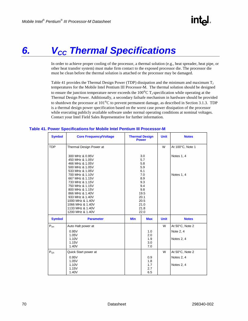
Mobile Intel® Pentium® III Processor-M Datasheet
70 Datasheet 298340-002
6. VCC Thermal Specifications In order to achieve proper cooling of the processor, a thermal solution (e.g., heat spreader, heat pipe, or other heat transfer system) must make firm contact to the exposed processor die. The processor die must be clean before the thermal solution is attached or the processor may be damaged.
Table 41 provides the Thermal Design Power (TDP) dissipation and the minimum and maximum TJ temperatures for the Mobile Intel Pentium III Processor-M. The thermal solution should be designed to ensure the junction temperature never exceeds the 100°C TJ specification while operating at the Thermal Design Power. Additionally, a secondary failsafe mechanism in hardware should be provided to shutdown the processor at 101°C to prevent permanent damage, as described in Section 3.1.3. TDP is a thermal design power specification based on the worst case power dissipation of the processor while executing publicly available software under normal operating conditions at nominal voltages. Contact your Intel Field Sales Representative for further information.
Table 41. Power Specifications for Mobile Intel Pentium III Processor-M
Symbol Core Frequency/Voltage Thermal Design Power
Unit Notes
TDP Thermal Design Power at 300 MHz & 0.95V 450 MHz & 1.05V 466 MHz & 1.05V 500 MHz & 1.05V 533 MHz & 1.05V 700 MHz & 1.10V 667 MHz & 1.15V 733 MHz & 1.15V 750 MHz & 1.15V 800 MHz & 1.15V 866 MHz & 1.40V 933 MHz & 1.40V 1000 MHz & 1.40V 1066 MHz & 1.40V 1133 MHz & 1.40V 1200 MHz & 1.40V
3.0 5.7 5.8 5.9 6.1 7.0 8.9 9.3 9.4 9.8 19.5 20.1 20.5 21.0 21.8 22.0
W
At 100°C, Note 1 Notes 1, 4 Notes 1, 4
Symbol Parameter Min Max Unit Notes
PAH Auto Halt power at 0.95V 1.05V 1.10V 1.15V 1.40V
1.0 2.0 1.9 3.0 7.0
W At 50°C, Note 2 Note 2, 4 Notes 2, 4
PQS Quick Start power at 0.95V 1.05V 1.10V 1.15V 1.40V
0.9 1.8 1.7 2.7 6.5
W At 50°C, Note 2 Notes 2, 4 Notes 2, 4

Mobile Intel® Pentium ® III Processor-M Datasheet
298340-002 Datasheet 71
PDSLP Deep Sleep power at 0.95V 1.05V 1.10V 1.15V 1.40V
0.7 1.3 1.2 2.0 4.8
W
At 35°C, Note 2 Notes 2, 4 Notes 2, 4
PDPRSLP Deeper Sleep power at 0.85V
0.62
W
At 35°C, Note 2
PDPRSLPULV Deeper Sleep power at 0.85V
0.47
W
At 35°C, Notes 2, 4
TJ Junction Temperature 0 100 °C Note 3 NOTES: 1. TDP is defined as the worst case power dissipated by the processor while executing publicly available software
under normal operating conditions at nominal voltages that meet the load line specifications. The TDP number shown is a specification based on Icc(maximum) and indirectly tested by Icc(maximum) testing. TDP definition is synonymous with the Thermal Design Power (typical) specification referred to in previous Intel datasheets. The Intel TDP specification is a recommended design point and is not representative of the absolute maximum power the processor may dissipate under worst case conditions.
2. Not 100% tested. These power specifications are determined by characterization of the processor currents at higher temperatures and extrapolating the values for the temperature indicated.
3. TJ is measured with the on-die thermal diode. 4. This specification applies only to the Ultra Low Voltage Mobile Intel Pentium III Processor-M.
6.1 Thermal Diode
The Mobile Intel Pentium III Processor-M has an on-die thermal diode that can be used to monitor the die temperature(TJ). A thermal sensor located on the motherboard, or a stand-alone measurement kit, may monitor the die temperature of the processor for thermal management or instrumentation purposes. Table 42 and Table 43 provide the diode interface and specifications.
Note: The reading of the thermal sensor connected to the thermal diode will not necessarily reflect the temperature of the hottest location on the die. This is due to inaccuracies in the thermal sensor, on-die temperature gradients between the location of the thermal diode and the hottest location on the die, and time based variations in the die temperature measurement. Time based variations can occur when the sampling rate of the thermal diode (by the thermal sensor) is slower than the rate at which the TJ temperature can change.
Table 42. Thermal Diode Interface
Signal Name Pin/Ball Number Signal Description
THERMDA AF13 Thermal diode anode
THERMDC AF14 Thermal diode cathode

Mobile Intel® Pentium® III Processor-M Datasheet
72 Datasheet 298340-002
Table 43. Thermal Diode Specifications
Symbol Parameter Min Typ Max Unit Notes
n Diode Ideality Factor (5-150uA) 1.0011 1.0067 1.0122 Notes 1, 2, 3, 4, 6
n Diode Ideality Factor (5-300uA) 1.0003 1.0091 1.0178 Notes 1, 2, 3, 5, 6 NOTES: 1. Intel does not support or recommend operation of the thermal diode under reverse bias. Intel does not support
or recommend operation of the thermal diode when the processor power supplies are not within their specified tolerance range.
2. Characterized at 100°C. 3. Not 100% tested. Specified by design/characterization. 4. Specified for Forward Bias Current = 5µA (min) and 150µA (max). 5. Specified for Forward Bias Current = 5µA (min) and 300µA (max). 6. The ideality factor, n, represents the deviation from ideal diode behavior as exemplified by the diode equation:
Where Is = saturation current, q = electronic charge, Vd = voltage across the diode, k = Boltzmann Constant, and T = absolute temperature (Kelvin).
−⋅= 1
qSFW
nkTVD
eII

Mobile Intel® Pentium ® III Processor-M Datasheet
298340-002 Datasheet 73
7. Processor Initialization and Configuration
7.1 Description The Mobile Intel Pentium III Processor-M has some configuration options that are determined by hardware and some that are determined by software. The processor samples its hardware configuration at reset on the active-to-inactive transition of RESET#. The P6 Family of Processors Developer’s Manual describes these configuration options. Some of the configuration options for the Mobile Intel Pentium III Processor-M are described in the remainder of this section.
7.1.1 Quick Start Enable Quick Start enabling is mandatory on the Mobile Intel Pentium III Processor-M by strapping A15# low. When the STPCLK# signal is asserted it will enter the Quick Start state when A15# is sampled active on the RESET# signal’s active-to-inactive transition. The Quick Start state supports snoops from the bus priority device but it does not support symmetric master snoops nor is the latching of interrupts supported. A “1” in bit position 5 of the Power-on Configuration register indicates that the Quick Start state has been enabled.
7.1.2 System Bus Frequency The current generation Mobile Intel Pentium III Processor-M will only function with a system bus frequency of 133 MHz. The Low Voltage Mobile Intel Pentium III Processor-M will support both 100-MHz and 133-MHz bus frequencies. The Ultra Low Voltage Mobile Intel Pentium III Processor-M will support both 100-MHz and 133-MHz bus frequencies (see product features section for specific supported frequencies). Bit positions 18 to 19 of the Power-on Configuration register indicates at which speed a processor will run.
7.1.3 APIC Enable The processor APIC must be hardware enabled by pulling the PICD[1:0] signals separately up to 1.5V and supplying an active PICCLK to the processor. Software can be used to disable the APIC if it is not being used, after PICD[1:0] are sampled high when RESET# is deasserted and the processor has started executing instructions.
7.2 Clock Frequencies and Ratios The Mobile Intel Pentium III Processor-M uses a clock design in which the bus clock is multiplied by a ratio to produce the processor’s internal (or “core”) clock. The ratio used is programmed into the processor during manufacturing. The bus ratio programmed into the processor is visible in bit positions

Mobile Intel® Pentium® III Processor-M Datasheet
74 Datasheet 298340-002
22 to 25 and 27 of the Power-on Configuration register. Table 22 shows the 5-bit codes in the Power-on Configuration register and their corresponding bus ratios.

Mobile Intel® Pentium ® III Processor-M Datasheet
298340-002 Datasheet 75
8. Processor Interface
8.1 Alphabetical Signal Reference
A[35:3]# (I/O – AGTL) The A[35:3]# (Address) signals define a 236-byte physical memory address space. When ADS# is active, these signals transmit the address of a transaction; when ADS# is inactive, these signals transmit transaction information. These signals must be connected to the appropriate pins/balls of both agents on the system bus. The A[35:24]# signals are protected with the AP1# parity signal, and the A[23:3]# signals are protected with the AP0# parity signal.
On the active-to-inactive transition of RESET#, each processor bus agent samples A[35:3]# signals to determine its power-on configuration. See P6 Family of Processors Developer’s Manual for details.
A20M# (I - 1.5V Tolerant) If the A20M# (Address-20 Mask) input signal is asserted, the processor masks physical address bit 20 (A20#) before looking up a line in any internal cache and before driving a read/write transaction on the bus. Asserting A20M# emulates the 8086 processor's address wrap-around at the 1-Mbyte boundary. Assertion of A20M# is only supported in Real mode.
ADS# (I/O - AGTL) The ADS# (Address Strobe) signal is asserted to indicate the validity of a transaction address on the A[35:3]# signals. Both bus agents observe the ADS# activation to begin parity checking, protocol checking, address decode, internal snoop or deferred reply ID match operations associated with the new transaction. This signal must be connected to the appropriate pins/balls on both agents on the system bus.
AERR# (I/O - AGTL) The AERR# (Address Parity Error) signal is observed and driven by both system bus agents, and if used, must be connected to the appropriate pins/balls of both agents on the system bus. AERR# observation is optionally enabled during power-on configuration; if enabled, a valid assertion of AERR# aborts the current transaction.
If AERR# observation is disabled during power-on configuration, a central agent may handle an assertion of AERR# as appropriate to the error handling architecture of the system.
AP[1:0]# (I/O - AGTL) The AP[1:0]# (Address Parity) signals are driven by the request initiator along with ADS#, A[35:3]#, REQ[4:0]# and RP#. AP1# covers A[35:24]#. AP0# covers A[23:3]#. A correct parity signal is high if an even number of covered signals is low and low if an odd number of covered signals are low. This allows parity to be high when all the covered signals are high. AP[1:0]# should be connected to the appropriate pins/balls on both agents on the system bus.
Mobile Intel® Pentium® III Processor-M Datasheet
76 Datasheet 298340-002
BCLK, BCLK# (I) The BCLK and BCLK# signals determines the system bus frequency.
On systems with Differential Clocking, both system bus agents must receive these signals to drive their outputs and latch their inputs on the BCLK rising edge and BCLK# falling edge. All external timing parameters are specified with respect to the crossing point of the BCLK rising edge and BCLK# falling edge.
On systems with Single Ended Clocking, both system bus agents must receive the BCLK signal to drive their outputs and latch their inputs on the BCLK rising edge. All external timing parameters are specified with respect to the BCLK signal. The BCLK# signal functions as the CLKREF input.
BERR# (I/O - AGTL) The BERR# (Bus Error) signal is asserted to indicate an unrecoverable error without a bus protocol violation. It may be driven by either system bus agent and must be connected to the appropriate pins/balls of both agents, if used. However, the Mobile Intel Pentium III Processor-Ms do not observe assertions of the BERR# signal.
BERR# assertion conditions are defined by the system configuration. Configuration options enable the BERR# driver as follows:
• Enabled or disabled
• Asserted optionally for internal errors along with IERR#
• Asserted optionally by the request initiator of a bus transaction after it observes an error
• Asserted by any bus agent when it observes an error in a bus transaction
BINIT# (I/O - AGTL) The BINIT# (Bus Initialization) signal may be observed and driven by both system bus agents and must be connected to the appropriate pins/balls of both agents, if used. If the BINIT# driver is enabled during the power-on configuration, BINIT# is asserted to signal any bus condition that prevents reliable future information.
If BINIT# is enabled during power-on configuration, and BINIT# is sampled asserted, all bus state machines are reset and any data which was in transit is lost. All agents reset their rotating ID for bus arbitration to the state after reset, and internal count information is lost. The L1 and L2 caches are not affected.
If BINIT# is disabled during power-on configuration, a central agent may handle an assertion of BINIT# as appropriate to the Machine Check Architecture (MCA) of the system.
BNR# (I/O - AGTL) The BNR# (Block Next Request) signal is used to assert a bus stall by any bus agent that is unable to accept new bus transactions. During a bus stall, the current bus owner cannot issue any new transactions.
Since multiple agents may need to request a bus stall simultaneously, BNR# is a wired-OR signal that must be connected to the appropriate pins/balls of both agents on the system bus. In order to avoid

Mobile Intel® Pentium ® III Processor-M Datasheet
298340-002 Datasheet 77
wire-OR glitches associated with simultaneous edge transitions driven by multiple drivers, BNR# is activated on specific clock edges and sampled on specific clock edges.
BP[3:2]# (I/O - AGTL) The BP[3:2]# (Breakpoint) signals are the System Support group Breakpoint signals. They are outputs from the processor that indicate the status of breakpoints.
BPM[1:0]# (I/O - AGTL) The BPM[1:0]# (Breakpoint Monitor) signals are breakpoint and performance monitor signals. They are outputs from the processor that indicate the status of breakpoints and programmable counters used for monitoring processor performance.
BPRI# (I - AGTL) The BPRI# (Bus Priority Request) signal is used to arbitrate for ownership of the system bus. It must be connected to the appropriate pins/balls on both agents on the system bus. Observing BPRI# active (as asserted by the priority agent) causes the processor to stop issuing new requests, unless such requests are part of an ongoing locked operation. The priority agent keeps BPRI# asserted until all of its requests are completed and then releases the bus by deasserting BPRI#.
BREQ0# (I/O - AGTL) The BREQ0# (Bus Request) signal is a processor Arbitration Bus signal. The processor indicates that it wants ownership of the system bus by asserting the BREQ0# signal.
During power-up configuration, the central agent must assert the BREQ0# bus signal. The processor samples BREQ0# on the active-to-inactive transition of RESET#. Optionally, this signal may be grounded with a 10-ohm resistor.
BSEL[1:0] (O – 3.3V Tolerant) The BSEL[1:0] (Select Processor System Bus Speed) signal is used to configure the processor for the system bus frequency. The chipset and system clock generator also uses the BSEL signals. The VTTPWRGD signal informs the processor to output the BSEL signals. During power up the BSEL signals will be indeterminate for a small period of time. The chipset and clock generator should not sample the BSEL signals until the VTTPWRGD signal is asserted. The assertion of the VTTPWRGD signal indicates that the BSEL signals are stable and driven to a final state by the processor. Please refer to Figure 12 for the timing relationship between the BSEL and VTTPWRGD signals.
Table 44 shows the encoding scheme for BSEL[1:0]. The only supported system bus frequency for the Mobile Intel Pentium III Processor-M is 133 MHz. The Low Voltage Mobile Intel Pentium III Processor-M will support both 100-MHz and 133-MHz bus frequencies. The Ultra Low Voltage Mobile Intel Pentium III Processor-M will support both 100-MHz and 133-MHz bus frequencies (see product features for specific supported frequencies). If another frequency is used then the processor is not guaranteed to function properly.

Mobile Intel® Pentium® III Processor-M Datasheet
78 Datasheet 298340-002
Table 44. BSEL[1:0] Encoding
BSEL[1:0] System Bus Frequency
01 100 MHz
11 133 MHz
CLKREF (Analog) The CLKREF (System Bus Clock Reference) signal provides a reference voltage to define the trip point for the BCLK signal on platforms supporting Single Ended Clocking. This signal should be connected to a resistor divider to generate 1.25V from the 2.5-V supply. A minimum of 1-uF decoupling capacitance is recommended on CLKREF. On systems with Differential Clocking, the CLKREF pin functions as the BCLK# input.
CMOSREF (Analog) The CMOSREF (CMOS Reference Voltage) signal provides a DC level reference voltage for the CMOS input buffers. CMOSREF must be generated from a stable 1.5-V supply and must meet the VCMOSREF specification. The same 1.5-V supply should be used to power the chipset CMOS I/O buffers that drive the CMOS signals. Please refer to the platform design guidelines for resistor divider recommendations.
D[63:0]# (I/O - AGTL) The D[63:0]# (Data) signals are the data signals. These signals provide a 64-bit data path between both system bus agents, and must be connected to the appropriate pins/balls on both agents. The data driver asserts DRDY# to indicate a valid data transfer.
DBSY# (I/O - AGTL) The DBSY# (Data Bus Busy) signal is asserted by the agent responsible for driving data on the system bus to indicate that the data bus is in use. The data bus is released after DBSY# is deasserted. This signal must be connected to the appropriate pins/balls on both agents on the system bus.
DEFER# (I - AGTL) The DEFER# (Defer) signal is asserted by an agent to indicate that the transaction cannot be guaranteed in-order completion. Assertion of DEFER# is normally the responsibility of the addressed memory agent or I/O agent. This signal must be connected to the appropriate pins/balls on both agents on the system bus.
DEP[7:0]# (I/O - AGTL) The DEP[7:0]# (Data Bus ECC Protection) signals provide optional ECC protection for the data bus. They are driven by the agent responsible for driving D[63:0]#, and must be connected to the appropriate pins/balls on both agents on the system bus if they are used. During power-on configuration, DEP[7:0]# signals can be enabled for ECC checking or disabled for no checking.
Mobile Intel® Pentium ® III Processor-M Datasheet
298340-002 Datasheet 79
DRDY# (I/O - AGTL) The DRDY# (Data Ready) signal is asserted by the data driver on each data transfer, indicating valid data on the data bus. In a multi-cycle data transfer, DRDY# can be deasserted to insert idle clocks. This signal must be connected to the appropriate pins/balls on both agents on the system bus.
DPSLP# (I - 1.5V Tolerant) The DPSLP# (Deep Sleep) signal, when asserted in the Quick Start state, causes the processor to enter the Deep Sleep state. In order to return to the Quick Start state BCLK, BCLK# must be running and the DPSLP# pin must be deasserted.
EDGCTRLP (I-Analog) The EDGCTRLP (Edge Rate Control) signal is used to configure the edge rate of the AGTL output buffers. Connect the signal to VSS with a 110-Ω, 1% resistor.
FERR# (O - 1.5V Tolerant Open-drain) The FERR# (Floating-point Error) signal is asserted when the processor detects an unmasked floating-point error. FERR# is similar to the ERROR# signal on the Intel 387 coprocessor, and it is included for compatibility with systems using DOS-type floating-point error reporting.
FLUSH# (I - 1.5V Tolerant) When the FLUSH# (Flush) input signal is asserted, the processor writes back all internal cache lines in the Modified state and invalidates all internal cache lines. At the completion of a flush operation, the processor issues a Flush Acknowledge transaction. The processor stops caching any new data while the FLUSH# signal remains asserted.
On the active-to-inactive transition of RESET#, each processor bus agent samples FLUSH# to determine its power-on configuration.
GHI# (I - 1.25V) The GHI# signal controls the selection of the operating mode bus ratio in a Mobile Intel Pentium III Processor-M. This signal is latched on exit from the Deep Sleep state and determines which of two bus ratios is selected for operation. This signal is ignored when the processor is not in the Deep Sleep state. This signal has an on-die pull-up to VCCT and should be driven with an Open-drain driver with no external pull-up.
HIT# (I/O - AGTL), HITM# (I/O - AGTL) The HIT# (Snoop Hit) and HITM# (Hit Modified) signals convey transaction snoop operation results, and must be connected to the appropriate pins/balls on both agents on the system bus. Either bus agent can assert both HIT# and HITM# together to indicate that it requires a snoop stall, which can be continued by reasserting HIT# and HITM# together.
IERR# (O - 1.5V Tolerant Open-drain) The IERR# (Internal Error) signal is asserted by the processor as the result of an internal error. Assertion of IERR# is usually accompanied by a SHUTDOWN transaction on the system bus. This transaction may optionally be converted to an external error signal (e.g., NMI) by system logic. The

Mobile Intel® Pentium® III Processor-M Datasheet
80 Datasheet 298340-002
processor will keep IERR# asserted until it is handled in software or with the assertion of RESET#, BINIT, or INIT#.
IGNNE# (I - 1.5V Tolerant) The IGNNE# (Ignore Numeric Error) signal is asserted to force the processor to ignore a numeric error and continue to execute non-control floating-point instructions. If IGNNE# is deasserted, the processor freezes on a non-control floating-point instruction if a previous instruction caused an error. IGNNE# has no affect when the NE bit in control register 0 (CR0) is set.
INIT# (I - 1.5V Tolerant) The INIT# (Initialization) signal is asserted to reset integer registers inside the processor without affecting the internal (L1 or L2) caches or the floating-point registers. The processor begins execution at the power-on reset vector configured during power-on configuration. The processor continues to handle snoop requests during INIT# assertion. INIT# is an asynchronous input.
If INIT# is sampled active on RESET#'s active-to-inactive transition, then the processor executes its built-in self test (BIST).
INTR (I - 1.5V Tolerant) The INTR (Interrupt) signal indicates that an external interrupt has been generated. INTR becomes the LINT0 signal when the APIC is enabled. The interrupt is maskable using the IF bit in the EFLAGS register. If the IF bit is set, the processor vectors to the interrupt handler after completing the current instruction execution. Upon recognizing the interrupt request, the processor issues a single Interrupt Acknowledge (INTA) bus transaction. INTR must remain active until the INTA bus transaction to guarantee its recognition.
LINT[1:0] (I - 1.5V Tolerant) The LINT[1:0] (Local APIC Interrupt) signals must be connected to the appropriate pins/balls of all APIC bus agents, including the processor and the system logic or I/O APIC component. When APIC is disabled, the LINT0 signal becomes INTR, a maskable interrupt request signal, and LINT1 becomes NMI, a non-maskable interrupt. INTR and NMI are backward compatible with the same signals for the Pentium processor. Both signals are asynchronous inputs.
Both of these signals must be software configured by programming the APIC register space to be used either as NMI/INTR or LINT[1:0] in the BIOS. If the APIC is enabled at reset, then LINT[1:0] is the default configuration.
LOCK# (I/O - AGTL) The LOCK# (Lock) signal indicates to the system that a sequence of transactions must occur atomically. This signal must be connected to the appropriate pins/balls on both agents on the system bus. For a locked sequence of transactions, LOCK# is asserted from the beginning of the first transaction through the end of the last transaction.
When the priority agent asserts BPRI# to arbitrate for bus ownership, it waits until it observes LOCK# deasserted. This enables the processor to retain bus ownership throughout the bus locked operation and guarantee the atomicity of lock.
Mobile Intel® Pentium ® III Processor-M Datasheet
298340-002 Datasheet 81
NC (No Connect) All signals named NC (No Connect) must be left unconnected.
NCTRL (I - Analog) The NCTRL signal provides the AGTL pull down impedance control. The processor samples this input to determine the N-channel pull-down device strength when it is the driving agent. An external 14 ohm (1% tolerance) pull-up resistor to VCCT is required for this signal. Please refer to platform design guide for implementation details.
NMI (I - 1.5V Tolerant) The NMI (Non-Maskable Interrupt) indicates that an external interrupt has been generated. NMI becomes the LINT1 signal when the APIC is disabled. Asserting NMI causes an interrupt with an internally supplied vector value of 2. An external interrupt-acknowledge transaction is not generated. If NMI is asserted during the execution of an NMI service routine, it remains pending and is recognized after the IRET is executed by the NMI service routine. At most, one assertion of NMI is held pending. NMI is rising edge sensitive.
PICCLK (I – 1.8V Tolerant) The PICCLK (APIC Clock) signal is an input clock to the processor and system logic or I/O APIC that is required for operation of the processor, system logic, and I/O APIC components on the APIC bus.
PICD[1:0] (I/O - 1.5V Tolerant Open-drain) The PICD[1:0] (APIC Data) signals are used for bi-directional serial message passing on the APIC bus. They must be connected to the appropriate pins/balls of all APIC bus agents, including the processor and the system logic or I/O APIC components. If the PICD0 signal is sampled low on the active-to-inactive transition of the RESET# signal, then the APIC is hardware disabled. For the Mobile Intel Pentium III Processor-M, the APIC is required to be hardware enabled as described in Section 7.1.3
PLL1, PLL2 (Analog) The PLL1 and PLL2 signals provide isolated analog decoupling is required for the internal PLL. See Section 3.2.2 for a description of the analog decoupling circuit.
PRDY# (O - AGTL) The PRDY# (Probe Ready) signal is a processor output used by debug tools to determine processor debug readiness.
PREQ# (I - 1.5V Tolerant) The PREQ# (Probe Request) signal is used by debug tools to request debug operation of the processor.
PWRGOOD (I – 1.8V Tolerant) PWRGOOD (Power Good) is a 1.8-V tolerant input. The processor requires this signal to be a clean indication that clocks and the power supplies (VCC, VCCT, etc.) are stable and within their specifications. Clean implies that the signal will remain low, (capable of sinking leakage current) and
Mobile Intel® Pentium® III Processor-M Datasheet
82 Datasheet 298340-002
without glitches, from the time that the power supplies are turned on, until they come within specification. The signal will then transition monotonically to a high (1.8V) state. Figure 12 through Figure 14 illustrate the relationship of PWRGOOD to other system signals. PWRGOOD can be driven inactive at any time, but clocks and power must again be stable before the rising edge of PWRGOOD. It must also meet the minimum pulse width specified in Table 24 (Section 3.7) and be followed by a 1 ms RESET# pulse.
The PWRGOOD signal, which must be supplied to the processor, is used to protect internal circuits against voltage sequencing issues. The PWRGOOD signal should be driven high throughout boundary scan operation.
REQ[4:0]# (I/O - AGTL) The REQ[4:0]# (Request Command) signals must be connected to the appropriate pins/balls on both agents on the system bus. They are asserted by the current bus owner when it drives A[35:3]# to define the currently active transaction type.
RESET# (I - AGTL) Asserting the RESET# signal resets the processor to a known state and invalidates the L1 and L2 caches without writing back Modified (M state) lines. For a power-on type reset, RESET# must stay active for at least 1 ms after VCC and BCLK, BCLK# have reached their proper DC and AC specifications and after PWRGOOD has been asserted. When observing active RESET#, all bus agents will deassert their outputs within two clocks. RESET# is the only AGTL signal that does not have on-die AGTL termination. A 56.2Ω 1% terminating resistor connected to VCCT is required.
A number of bus signals are sampled at the active-to-inactive transition of RESET# for the power-on configuration. The configuration options are described in Section 4 and in the P6 Family of Processors Developer’s Manual.
Unless its outputs are tri-stated during power-on configuration, after an active-to-inactive transition of RESET#, the processor optionally executes its built-in self-test (BIST) and begins program execution at reset-vector 000FFFF0H or FFFFFFF0H. RESET# must be connected to the appropriate pins/balls on both agents on the system bus.
RP# (I/O - AGTL) The RP# (Request Parity) signal is driven by the request initiator and provides parity protection on ADS# and REQ[4:0]#. RP# should be connected to the appropriate pins/balls on both agents on the system bus.
A correct parity signal is high if an even number of covered signals is low and low if an odd number of covered signals are low. This definition allows parity to be high when all covered signals are high.
RS[2:0]# (I/O - AGTL) The RS[2:0]# (Response Status) signals are driven by the response agent (the agent responsible for completion of the current transaction) and must be connected to the appropriate pins/balls on both agents on the system bus.

Mobile Intel® Pentium ® III Processor-M Datasheet
298340-002 Datasheet 83
RSP# (I - AGTL) The RSP# (Response Parity) signal is driven by the response agent (the agent responsible for completion of the current transaction) during assertion of RS[2:0]#. RSP# provides parity protection for RS[2:0]#. RSP# should be connected to the appropriate pins/balls on both agents on the system bus.
A correct parity signal is high if an even number of covered signals are low, and it is low if an odd number of covered signals are low. During Idle state of RS[2:0]# (RS[2:0]#=000), RSP# is also high since it is not driven by any agent guaranteeing correct parity.
RTTIMPEDP (I-Analog) The RTTIMPEDP (RTT Impedance/PMOS) signal is used to configure the on-die AGTL termination. Connect the RTTIMPEDP signal to VSS with a 56.2-Ω, 1% resistor.
SMI# (I - 1.5V Tolerant) The SMI# (System Management Interrupt) is asserted asynchronously by system logic. On accepting a System Management Interrupt, the processor saves the current state and enters System Management Mode (SMM). An SMI Acknowledge transaction is issued, and the processor begins program execution from the SMM handler.
STPCLK# (I - 1.5V Tolerant) The STPCLK# (Stop Clock) signal, when asserted, causes the processor to enter a low-power Quick Start state. The processor issues a Stop Grant Acknowledge special transaction and stops providing internal clock signals to all units except the bus and APIC units. The processor continues to snoop bus transactions and service interrupts while in the Quick Start state. When STPCLK# is deasserted and other conditions in are met, the processor restarts its internal clock to all units and resumes execution. The assertion of STPCLK# has no affect on the bus clock.
TCK (I - 1.5V Tolerant) The TCK (Test Clock) signal provides the clock input for the test bus (also known as the test access port).
TDI (I - 1.5V Tolerant) The TDI (Test Data In) signal transfers serial test data to the processor. TDI provides the serial input needed for JTAG support.
TDO (O - 1.5V Tolerant Open-drain) The TDO (Test Data Out) signal transfers serial test data from the processor. TDO provides the serial output needed for JTAG support.
TESTHI[2:1] (I - 1.25V Tolerant) The TESTHI[2:1] (Test input High) signals are used during processor test and need to be pulled high during normal operation.

Mobile Intel® Pentium® III Processor-M Datasheet
84 Datasheet 298340-002
TESTLO[2:1] (I - 1.5V Tolerant) The TESTLO[2:1] (Test input Low) signals are used during processor test and needs to be pulled to ground during normal operation.
THERMDA, THERMDC (Analog) The THERMDA (Thermal Diode Anode) and THERMDC (Thermal Diode Cathode) signals connect to the anode and cathode of the on-die thermal diode.
TMS (I - 1.5V Tolerant) The TMS (Test Mode Select) signal is a JTAG support signal used by debug tools.
TRDY# (I/O - AGTL) The TRDY# (Target Ready) signal is asserted by the target to indicate that the target is ready to receive write or implicit write-back data transfer. TRDY# must be connected to the appropriate pins/balls on both agents on the system bus.
TRST# (I - 1.5V Tolerant) The TRST# (Test Reset) signal resets the Test Access Port (TAP) logic. The Mobile Intel Pentium III Processor-Ms do not self-reset during power on; therefore, it is necessary to drive this signal low during power-on reset.
VID[4:0] (O – Open-drain) The VID[4:0] (Voltage ID) pins/balls can be used to support automatic selection of power supply voltages. Please refer to Section 3.2.2 for details.
VREF (Analog) The VREF (AGTL Reference Voltage) signal provides a DC level reference voltage for the AGTL input buffers. A voltage divider should be used to divide VCCT by 2/3. Resistor values of 1.00 kΩ and 2.00 kΩ are recommended. Decouple the VREF signal with three 0.1-µF high-frequency capacitors close to the processor.
VTTPWRGD (I – 1.25V) The VTTPWRGD signal informs the processor to output the VID signals. During power up, the VID signals will be in an indeterminate state for a small period of time. The voltage regulator should not sample and/or latch the VID signals until the VTTPWRGD signal is asserted. The assertion of the VTTPWRGD signal indicates that the VID signals are stable and are driven to the final state by the processor. Please refer to Figure 12 for the power up sequence.

Mobile Intel® Pentium ® III Processor-M Datasheet
298340-002 Datasheet 85
8.2 Signal Summaries
Table 45. Input Signals
Name Active Level Clock Signal Group Qualified
A20M# Low Asynch CMOS Always
BCLK High — System Bus Always
BCLK# Low — System Bus Always
BPRI# Low BCLK System Bus Always
DEFER# Low BCLK System Bus Always
DPSLP# Low Asynch Implementation Quick Start state
FLUSH# Low Asynch CMOS Always
GHI# Low Asynch CMOS Deep Sleep state
IGNNE# Low Asynch CMOS Always
INIT# Low Asynch System Bus Always
INTR High Asynch CMOS APIC disabled mode
LINT[1:0] High Asynch APIC APIC enabled mode
NMI High Asynch CMOS APIC disabled mode
NCTRL High Asynch
PICCLK High — APIC Always
PREQ# Low Asynch Implementation Always
PWRGOOD High Asynch Implementation Always
RESET# Low BCLK System Bus Always
RSP# Low BCLK System Bus Always
SMI# Low Asynch CMOS Always
STPCLK# Low Asynch Implementation Always
TCK High — JTAG
TDI TCK JTAG
TMS TCK JTAG
TRST# Low Asynch JTAG
VTTPWRGD High Asynch Power/Other
Table 46. Output Signals
Name Active Level Clock Signal Group
BSEL[1:0] High Asynch Open-drain
FERR# Low Asynch Open-drain
IERR# Low Asynch Open-drain
PRDY# Low BCLK Implementation
TDO High TCK JTAG
VID[4:0] High Asynch Power/Other

Mobile Intel® Pentium® III Processor-M Datasheet
86 Datasheet 298340-002
Table 47. Input/Output Signals (Single Driver)
Name Active Level Clock Signal Group Qualified
A[35:3]# Low BCLK System Bus ADS#, ADS#+1
ADS# Low BCLK System Bus Always
AP[1:0]# Low BCLK System Bus ADS#, ADS#+1
BREQ0# Low BCLK System Bus Always
BP[3:2]# Low BCLK System Bus Always
BPM[1:0]# Low BCLK System Bus Always
D[63:0]# Low BCLK System Bus DRDY#
DBSY# Low BCLK System Bus Always
DEP[7:0]# Low BCLK System Bus DRDY#
DRDY# Low BCLK System Bus Always
LOCK# Low BCLK System Bus Always
REQ[4:0]# Low BCLK System Bus ADS#, ADS#+1
RP# Low BCLK System Bus ADS#, ADS#+1
RS[2:0]# Low BCLK System Bus Always
TRDY# Low BCLK System Bus Response phase
Table 48. Input/Output Signals (Multiple Driver)
Name Active Level Clock Signal Group Qualified
AERR# Low BCLK System Bus ADS#+3
BERR# Low BCLK System Bus Always
BINIT# Low BCLK System Bus Always
BNR# Low BCLK System Bus Always
HIT# Low BCLK System Bus Always
HITM# Low BCLK System Bus Always
PICD[1:0] High PICCLK APIC Always

Mobile Intel® Pentium ® III Processor-M Datasheet
298340-002 Datasheet 87
Appendix A. PLL RLC Filter Specification
A1. Introduction All Mobile Intel Pentium III Processor-Ms have internal PLL clock generators, which are analog in nature and require quiet power supplies for minimum jitter. Jitter is detrimental to a system; it degrades external I/O timings as well as internal core timings (i.e. maximum frequency). The PLL RLC filter specifications for the Mobile Intel Pentium III Processor-M are the same as those for the mobile Pentium III processor. The general desired topology is shown in Figure 2. Excluded from the external circuitry are parasitics associated with each component.
A2. Filter Specification The function of the filter is two fold. It protects the PLL from external noise through low-pass attenuation. It also protects the PLL from internal noise through high-pass filtering. In general, the low-pass description forms an adequate description for the filter.
The AC low-pass specification, with input at VCCT and output measured across the capacitor, is as follows:
• < 0.2-dB gain in pass band
• < 0.5-dB attenuation in pass band < 1 Hz (see DC drop in next set of requirements)
• 34-dB attenuation from 1 MHz to 66 MHz
• 28-dB attenuation from 66 MHz to core frequency
• The filter specification (AC) is graphically shown in Figure 29.
Other requirements:
• Use a shielded type inductor to minimize magnetic pickup
• The filter should support a DC current of at least 30 mA
• The DC voltage drop from VCCT to PLL1 should be less than 60 mV, which in practice implies series resistance of less than 2Ω. This also means that the pass band (from DC to 1 Hz) attenuation below 0.43 dB for VCCT = 1.25V.
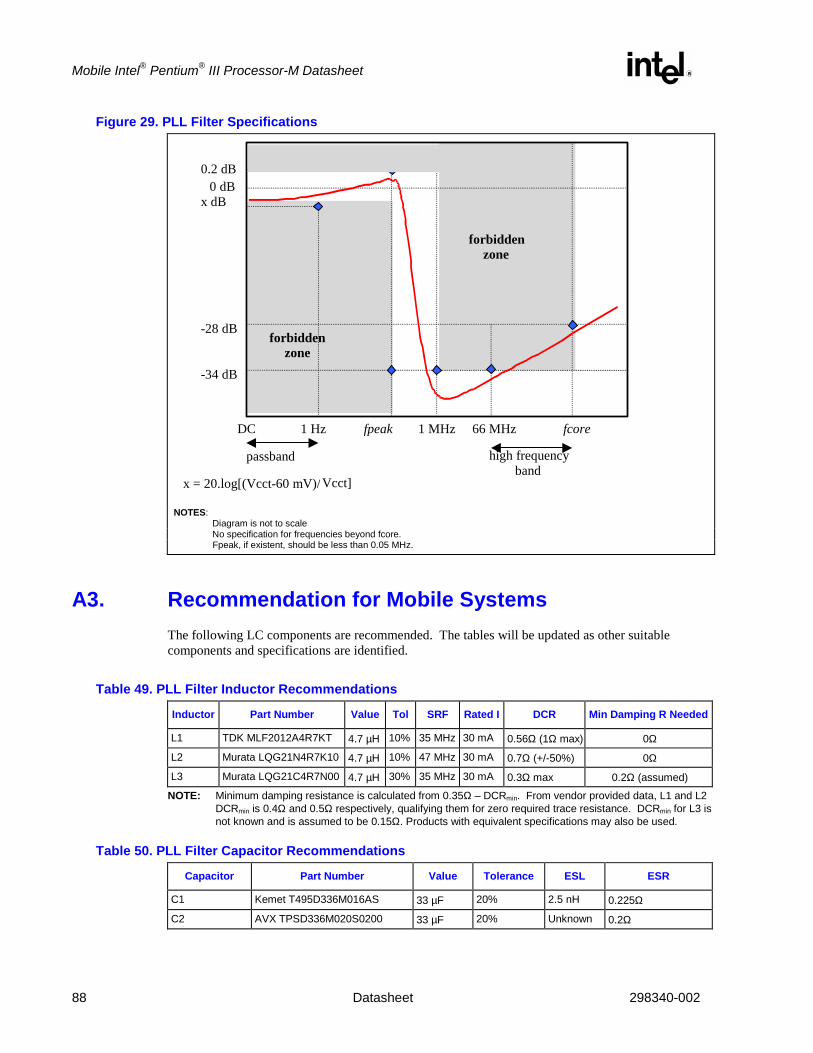
Mobile Intel® Pentium® III Processor-M Datasheet
88 Datasheet 298340-002
Figure 29. PLL Filter Specifications
0 dB
-28 dB
-34 dB
0.2 dB
forbiddenzone
x dB
forbiddenzone
1 MHz 66 MHz fcorefpeak1 HzDC
passband high frequencyband
x = 20.log[(Vcct-60 mV)/Vcct]
NOTES: Diagram is not to scale No specification for frequencies beyond fcore. Fpeak, if existent, should be less than 0.05 MHz.
A3. Recommendation for Mobile Systems The following LC components are recommended. The tables will be updated as other suitable components and specifications are identified.
Table 49. PLL Filter Inductor Recommendations
Inductor Part Number Value Tol SRF Rated I DCR Min Damping R Needed
L1 TDK MLF2012A4R7KT 4.7 µH 10% 35 MHz 30 mA 0.56Ω (1Ω max) 0Ω
L2 Murata LQG21N4R7K10 4.7 µH 10% 47 MHz 30 mA 0.7Ω (+/-50%) 0Ω
L3 Murata LQG21C4R7N00 4.7 µH 30% 35 MHz 30 mA 0.3Ω max 0.2Ω (assumed) NOTE: Minimum damping resistance is calculated from 0.35Ω – DCRmin. From vendor provided data, L1 and L2
DCRmin is 0.4Ω and 0.5Ω respectively, qualifying them for zero required trace resistance. DCRmin for L3 is not known and is assumed to be 0.15Ω. Products with equivalent specifications may also be used.
Table 50. PLL Filter Capacitor Recommendations
Capacitor Part Number Value Tolerance ESL ESR
C1 Kemet T495D336M016AS 33 µF 20% 2.5 nH 0.225Ω
C2 AVX TPSD336M020S0200 33 µF 20% Unknown 0.2Ω

Mobile Intel® Pentium ® III Processor-M Datasheet
298340-002 Datasheet 89
Table 51. PLL Filter Resistor Recommendations
Resistor Part Number Value Tolerance Power
R1 Various 1Ω 10% 1/16W
To satisfy damping requirements, total series resistance in the filter (from VCCT to the top plate of the capacitor) must be at least 0.35Ω. This resistor can be in the form of a discrete component, or routing, or both. For example, if the picked inductor has minimum DCR of 0.25Ω, then a routing resistance of at least 0.10Ω is required. Be careful not to exceed the maximum resistance rule (2Ω). For example, if using discrete R1, the maximum DCR of the L should be less than 2.0 - 1.1 = 0.9Ω, which precludes using L2 and possibly L1.
Other routing requirements include:
• The capacitor should be close to the PLL1 and PLL2 pins, with less than 0.1Ω per route (These routes do not count towards the minimum damping resistance requirement).
• The PLL2 route should be parallel and next to the PLL1 route (minimize loop area).
• The inductor should be close to the capacitor; any routing resistance should be inserted between VCCT and the inductor.
• Any discrete resistor should be inserted between VCCT and the inductor.
A4. Comments • A magnetically shielded inductor protects the circuit from picking up external flux noise. This
should provide better timing margins than with an unshielded inductor.
• A discrete or routed resistor is required because the LC filter by nature has an under-damped response, which can cause resonance at the LC pole. Noise amplification at this band, although not in the PLL-sensitive spectrum, could cause a fatal headroom reduction for analog circuitry. The resistor serves to dampen the response. Systems with tight space constraints should consider a discrete resistor to provide the required damping resistance. Too large of a damping resistance can cause a large IR drop, which means less analog headroom and lower frequency.
• Ceramic capacitors have very high self-resonance frequencies, but they are not available in large capacitance values. A high self-resonant frequency coupled with low ESL/ESR is crucial for sufficient rejection in the PLL and high frequency band. The recommended tantalum capacitors have acceptably low ESR and ESL.
• The capacitor must be close to the PLL1 and PLL2 pins; otherwise the value of the low ESR tantalum capacitor is wasted. Note the distance constraint should be translated from the 0.1-Ω requirement.