Embed Size (px)
Citation preview
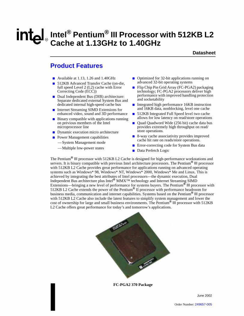
Intel® Pentium® III Processor with 512KB L2 Cache at 1.13GHz to 1.40GHz
Datasheet
Product Features
The Pentium® III processor with 512KB L2 Cache is designed for high-performance workstations and servers. It is binary compatible with previous Intel architecture processors. The Pentium® III processor with 512KB L2 Cache provides great performance for applications running on advanced operating systems such as Windows* 98, Windows* NT, Windows* 2000, Windows* Me and Linux. This is achieved by integrating the best attributes of Intel processors—the dynamic execution, Dual Independent Bus architecture plus Intel® MMX™ technology and Internet Streaming SIMD Extensions—bringing a new level of performance for systems buyers. The Pentium® III processor with 512KB L2 Cache extends the power of the Pentium® II processor with performance headroom for business media, communication and internet capabilities. Systems based on the Pentium® III processor with 512KB L2 Cache also include the latest features to simplify system management and lower the cost of ownership for large and small business environments. The Pentium® III processor with 512KB L2 Cache offers great performance for today’s and tomorrow’s applications.
FC-PGA2 370 Package
Available at 1.13, 1.26 and 1.40GHz 512KB Advanced Transfer Cache (on-die,
full speed Level 2 (L2) cache with Error Correcting Code (ECC))
Dual Independent Bus (DIB) architecture: Separate dedicated external System Bus and dedicated internal high-speed cache bus
Internet Streaming SIMD Extensions for enhanced video, sound and 3D performance
Binary compatible with applications running on previous members of the Intel microprocessor line
Dynamic execution micro architecture Power Management capabilities
—System Management mode
—Multiple low-power states
Optimized for 32-bit applications running on advanced 32-bit operating systems
Flip Chip Pin Grid Array (FC-PGA2) packaging technology; FC-PGA2 processors deliver high performance with improved handling protection and socketability
Integrated high performance 16KB instruction and 16KB data, nonblocking, level one cache
512KB Integrated Full Speed level two cache allows for low latency on read/store operations
Quad Quadword Wide (256 bit) cache data bus provides extremely high throughput on read/store operations.
8-way cache associativity provides improved cache hit rate on reads/store operations.
Error-correcting code for System Bus data Data Prefetch Logic
June 2002
Order Number: 249657-005
Intel® Pentium® III Processor with 512KB L2 Cache at 1.13GHz to 1.40GHz
2
Information in this dproperty rights is grwhatsoever, and Intfitness for a particuintended for use in
Intel may make cha
Designers must notfuture definition and
The Pentium® III Prpublished specifica
Contact your local I
Copies of documen548-4725 or by visi
All rights reserved. States or other cou
Copyright © Intel C
* Other names and
Datasheet
ocument is provided in connection with Intel products. No license, express or implied, by estoppel or otherwise, to any intellectual anted by this document. Except as provided in Intel’s Terms and Conditions of Sale for such products, Intel assumes no liability el disclaims any express or implied warranty, relating to sale and/or use of Intel products including liability or warranties relating to lar purpose, merchantability, or infringement of any patent, copyright or other intellectual property right. Intel products are not medical, life saving, or life sustaining applications.
nges to specifications and product descriptions at any time, without notice.
rely on the absence or characteristics of any features or instructions marked "reserved" or "undefined." Intel reserves these for shall have no responsibility whatsoever for conflicts or incompatibilities arising from future changes to them.
ocessor with 512KB L2 Cache may contain design defects or errors known as errata which may cause the product to deviate from tions. Current characterized errata are available on request.
ntel sales office or your distributor to obtain the latest specifications and before placing your product order.
ts which have an ordering number and are referenced in this document, or other Intel literature may be obtained by calling 1-800-ting Intel’s website at http://www.intel.com.
Intel, the Intel Logo and Pentium are trademarks or registered trademarks of Intel Corporation or its subsidiaries in the United ntries.
orporation, 2002
brands may be claimed as the property of others.
Intel® Pentium® III Processor with 512KB L2 Cache at 1.13GHz to 1.40GHz
Contents1.0 Introduction ..................................................................................................................1
1.1 Terminology...........................................................................................................21.1.1 Package and Processor Terminology ......................................................21.1.2 Processor Naming Convention.................................................................3
1.2 Related Documents...............................................................................................41.3 Revision History ....................................................................................................4
2.0 Electrical Specifications..........................................................................................5
2.1 Processor System Bus and VREF ............................................................................................ 52.2 Clock Control and Low Power States....................................................................6
2.2.1 Normal State—State 1 .............................................................................72.2.2 AutoHALT Powerdown State—State 2.....................................................72.2.3 Stop-Grant State—State 3 .......................................................................82.2.4 HALT/Grant Snoop State—State 4 ..........................................................82.2.5 Sleep State—State 5................................................................................82.2.6 Deep Sleep State—State 6 ......................................................................92.2.7 Clock Control............................................................................................9
2.3 Power and Ground Pins ......................................................................................102.3.1 Phase Lock Loop (PLL) Power...............................................................10
2.4 Decoupling Guidelines ........................................................................................112.4.1 Processor VCCCORE Decoupling............................................................11
2.5 Processor System Bus Clock and Processor Clocking .......................................112.6 Voltage Identification ...........................................................................................122.7 Processor System Bus Unused Pins...................................................................152.8 Processor System Bus Signal Groups ................................................................15
2.8.1 Asynchronous vs. Synchronous for System Bus Signals.......................162.8.2 System Bus Frequency Select Signals ..................................................17
2.9 ............................................................................................... Maximum Ratings182.10 Processor Voltage Level Specifications ..............................................................182.11 AGTL System Bus Specifications........................................................................242.12 System Bus Timing Specifications ......................................................................24
3.0 Signal Quality Specifications ..............................................................................37
3.1 BCLK/BCLK# & PICCLK Signal Quality Specifications and Measurement Guide-lines37
3.2 AGTL Signal Quality Specifications and Measurement Guidelines.....................383.3 AGTL Signal Quality Specifications and Measurement Guidelines.....................39
3.3.1 Overshoot/Undershoot Guidelines .........................................................393.3.2 Overshoot/Undershoot Magnitude .........................................................403.3.3 Overshoot/Undershoot Pulse Duration...................................................403.3.4 Activity Factor.........................................................................................403.3.5 Reading Overshoot/Undershoot Specification Tables............................413.3.6 Determining if a System Meets the Overshoot/Undershoot Specifications
423.4 Non-AGTL Signal Quality Specifications and Measurement Guidelines.............44
3.4.1 Overshoot/Undershoot Guidelines .........................................................443.4.2 Ringback Specification ...........................................................................453.4.3 Settling Limit Guideline...........................................................................45
Datasheet 3
Intel® Pentium® III Processor with 512KB L2 Cache at 1.13GHz to 1.40GHz
4.0 Thermal Specifications and Design Considerations ................................. 47
4.1 Thermal Specifications........................................................................................ 474.1.1 THERMTRIP# Requirement................................................................... 474.1.2 Thermal Diode........................................................................................ 48
4.2 Thermal Metrology .............................................................................................. 48
5.0 Mechanical Specifications ................................................................................... 49
5.1 FC-PGA2 Mechanical Specifications ..................................................................495.2 Recommended Mechanical Keep-Out Zones ..................................................... 525.3 Processor Markings ............................................................................................535.4 Processor Signal Listing......................................................................................54
6.0 Boxed Processor Specifications ....................................................................... 70
6.1 Mechanical Specifications................................................................................... 716.1.1 Mechanical Specifications for the FC-PGA2 Package ........................... 716.1.2 Boxed Processor Heatsink Weight......................................................... 72
6.2 Thermal Specifications........................................................................................ 736.2.1 Boxed Processor Cooling Requirements ...............................................736.2.2 Boxed Processor Thermal Cooling Solution Clip ................................... 73
6.3 Electrical Requirements for the Boxed Intel® Pentium® III Processor with 512KB L2 Cache746.3.1 Electrical Requirements .........................................................................74
7.0 Processor Signal Description ............................................................................. 76
7.1 Alphabetical Signals Reference .......................................................................... 767.2 Signal Summaries ............................................................................................... 84
4 Datasheet
Intel® Pentium® III Processor with 512KB L2 Cache at 1.13GHz to 1.40GHz
List of Figures1 Integrated Heat Spreader (IHS) ............................................................................12 AGTL Bus Topology ..............................................................................................63 Stop Clock State Machine .....................................................................................74 PLL Filter Specification........................................................................................105 Differential/Single-Ended Clocking Example.......................................................126 VTT Power Good and Bus Select Interconnect Diagram .....................................147 BSEL[1:0] Example for a System Design............................................................178 Vcc Static & Transient Tolerance ........................................................................229 Clock Waveform..................................................................................................3210 BCLK/BCLK#, PICCLK, and TCK Generic Clock Waveform ..............................3211 System Bus Valid Delay Timings ........................................................................3312 System Bus Setup and Hold Timings..................................................................3313 System Bus Reset and Configuration Timings....................................................3414 Platform Power-On Sequence and Timings ........................................................3416 Test Timings (TAP Connection) ..........................................................................3515 Power-On Reset and Configuration Timings.......................................................3517 Test Reset Timings .............................................................................................3618 BCLK/BCLK#, PICCLK Generic Clock Waveform at the Processor Pins ...........3819 Low to High AGTL Receiver Ringback Tolerance...............................................3920 Maximum Acceptable AGTL Overshoot/Undershoot Waveform .........................4321 Non-AGTL Overshoot/Undershoot, Settling Limit, and Ringback 1 ....................4422 Package Dimensions...........................................................................................5023 FC-PGA2 IHS Flatness Specification..................................................................5224 Volumetric Keep-Out ...........................................................................................5225 Component Keep-Out .........................................................................................5326 Top Side Processor Markings .............................................................................5327 Intel® Pentium® III processor with 512KB L2 Cache Pinout ..............................5428 Conceptual Boxed Intel® Pentium® III Processor with 512KB L2 Cache for the
PGA370 Socket7029 Comparison between FC-PGA and FC-PGA2 package......................................7131 Dimensions of Mechanical Step Feature in Heatsink Base.................................7230 Side View of Space Requirements for the Boxed Processor ..............................7232 Thermal Airspace Requirement for all Boxed Intel® Pentium® III Processor with
512KB L2 Cache Fan Heatsinks in the PGA370 Socket7333 Boxed Processor Fan Heatsink Power Cable Connector Description.................7434 Motherboard Power Header Placement Relative to the Boxed Intel® Pentium® III
Processor with 512KB L2 Cache75
Datasheet 5
Intel® Pentium® III Processor with 512KB L2 Cache at 1.13GHz to 1.40GHz
List of Tables1 Processor Identification......................................................................................... 32 System Bus Clock in Deep Sleep Mode (Differential Mode only)1 .......................93 Voltage Identification Definition 1................................................................................................... 13
4 System Bus Signal Groups 1 .............................................................................. 165 Frequency Select Truth Table for BSEL[1:0] ...................................................... 186 Absolute Maximum Ratings ................................................................................ 187 Power Supply Current Slew Rate (dIcccore/dt)................................................... 218 Vcc Static & Transient Tolerance........................................................................ 229 AGTL Signal Group Levels Specifications 1 ....................................................... 2310 Non-AGTL Signal Group Levels Specifications 1 .................................................................. 23
11 3.3 Volt CMOS Output Signal Group DC Specifications ..................................... 2412 Processor AGTL Bus Specifications 1, 2 ....................................................................................24
13 System Bus Timing Specifications (Single-Ended Clock)1,4 .............................. 2614 System Bus Timing Specifications (Differential Clock)1, 2, 6 ............................................ 27
15 System Bus Timing Specifications (AGTL Signal Group)1, 2, 3....................................... 27
16 System Bus Timing Specifications (CMOS Signal Group) 1, 2, 3, 4................................ 28
17 System Bus Timing Specifications (Reset Conditions) 1................................................... 29
18 System Bus Timing Specifications (APIC Clock and APIC I/O)1, 2, 3........................... 29
19 System Bus Timing Specifications (TAP Connection)1, 2, 3.............................................. 30
20 Platform Power-On Timings2 .............................................................................. 3121 BCLK (Single-Ended Clock Mode) Signal Quality Specifications for Simulation at
the Processor Pins13722 BCLK/BCLK# (Differential Clock Mode) and PICCLK Signal Quality Specifications
for Simulation at the Processor Pins 137
23 AGTL Signal Groups Ringback Tolerance Specifications at the Processor Pins 1, 2, 338
24 Example Platform Information............................................................................. 4125 133 MHz AGTL Signal Group Overshoot/Undershoot Tolerance 1, 2, 3 ............ 4326 33 MHz CMOS Signal Group Overshoot/Undershoot Tolerance........................ 4527 Signal Ringback Specifications for Non-AGTL Signal Simulation at the Processor
Pins 14528 THERMTRIP# Time Requirement....................................................................... 4729 Thermal Diode Parameters1............................................................................................................ 48
30 Thermal Diode Interface......................................................................................4831 Intel® Pentium® III processor with 512KB L2 Cache Package Dimensions....... 5132 Processor Case Loading Parameters ................................................................. 5133 Signal Listing in Order by Signal Name .............................................................. 5533 Signal Listing in Order by Signal Name .............................................................. 5734 Signal Listing in Order by Pin Number ................................................................ 6235 Boxed Processor Fan Heatsink Spatial Dimensions........................................... 7236 Fan Heatsink Power and Signal Specifications................................................... 7437 Signal Description ............................................................................................... 7638 Output Signals..................................................................................................... 8439 Input Signals ....................................................................................................... 8440 Input/Output Signals (Single Driver).................................................................... 8641 Input/Output Signals (Multiple Driver) ................................................................. 86
6 Datasheet

Intel® Pentium® III Processor with 512KB L2 Cache at 1.13GHz to 1.40GHz
Datasheet 7

Intel® Pentium® III Processor with 512KB L2 Cache at 1.13GHz to 1.40GHz
Datasheet 8
Intel® Pentium® III Processor with 512KB L2 Cache at 1.13GHz to 1.40GHz
1.0 Introduction
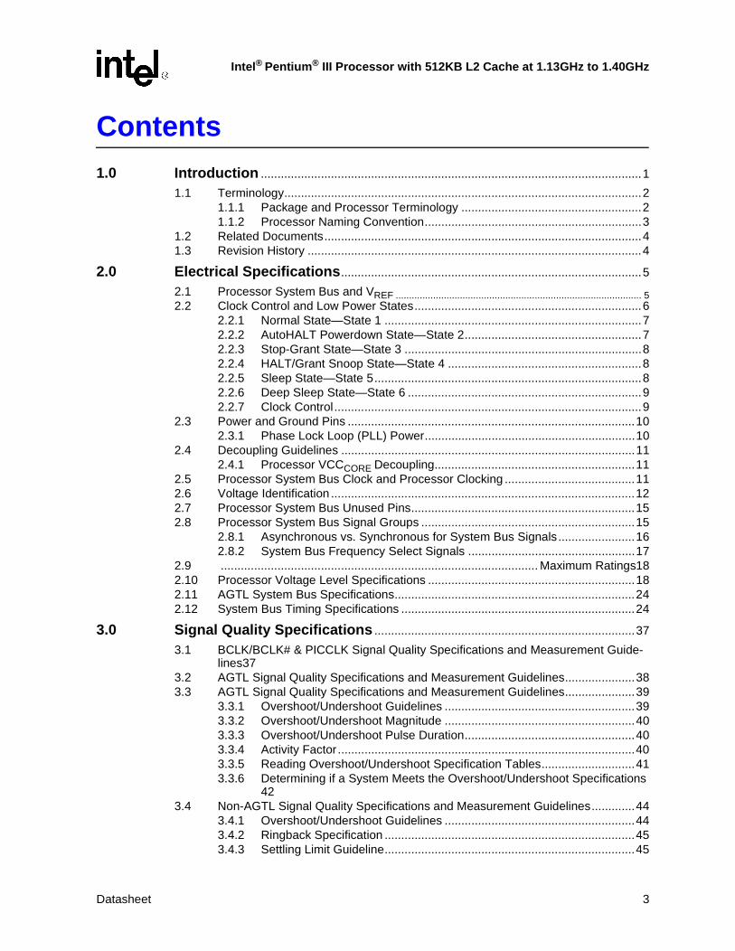
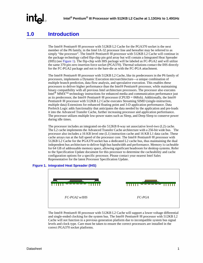
The Intel® Pentium® III processor with 512KB L2 Cache for the PGA370 socket is the next member of the P6 family, in the Intel IA-32 processor line and hereafter may be referred to as simply “the processor”. The Intel® Pentium® III processor with 512KB L2 Cache will continue in the package technology called flip-chip pin grid array but will contain a Integrated Heat Spreader (IHS) (see Figure 1). The flip-chip with IHS package will be labeled as FC-PGA2 and will utilize the same 370-pin zero insertion force socket (PGA370). Thermal solutions contact the IHS directly for the FC-PGA2 package and not to the bare-die as with the FC-PGA attachment.
The Intel® Pentium® III processor with 512KB L2 Cache, like its predecessors in the P6 family of processors, implements a Dynamic Execution microarchitecture—a unique combination of multiple branch prediction, data flow analysis, and speculative execution. This enables these processors to deliver higher performance than the Intel® Pentium® processor, while maintaining binary compatibility with all previous Intel architecture processors. The processor also executes Intel® MMXTM technology instructions for enhanced media and communication performance just as its predecessor, the Intel® Pentium® III processor (CPUID = 068xh). Additionally, the Intel® Pentium® III processor with 512KB L2 Cache executes Streaming SIMD (single-instruction, multiple data) Extensions for enhanced floating point and 3-D application performance. Data Prefetch Logic adds functionality that anticipates the data needed by the application and pre-loads it into the Advanced Transfer Cache, further increasing processor and application performance. The processor utilizes multiple low-power states such as Sleep, and Deep Sleep to conserve power during idle times.
The processor includes an integrated on-die 512KB 8-way set associative level-two (L2) cache. The L2 cache implements the Advanced Transfer Cache architecture with a 256-bit wide bus. The processor also includes a 16 KB level one (L1) instruction cache and 16 KB L1 data cache. These cache arrays run at the full speed of the processor core. The Intel® Pentium® III processor with 512KB L2 Cache for the PGA370 socket has a dedicated L2 cache bus, thus maintaining the dual independent bus architecture to deliver high bus bandwidth and performance. Memory is cacheable for 64 GB of addressable memory space, allowing significant headroom for desktop systems. Refer to the Specification Update document for this processor to determine the cacheability and cache configuration options for a specific processor. Please contact your nearest Intel Sales Representative for the latest Processor Specification Update.
The Intel® Pentium® III processor with 512KB L2 Cache will support a lower voltage differential and single-ended clocking for the system bus. The Intel® Pentium® III processor with 512KB L2 Cache will not function in a previous generation platform due to incompatible system bus signal levels and clock type. Care must be taken to ensure the correct processors are installed in the correct PGA370 socket platforms.
Figure 1. Integrated Heat Spreader (IHS)
FC-PGA2 w/IHS FC-PGA
Datasheet 1
Intel® Pentium® III Processor with 512KB L2 Cache at 1.13GHz to 1.40GHz
1.1 Terminology
In this document, a ‘#’ symbol after a signal name refers to an active low signal. This means that a signal is in the active state (based on the name of the signal) when driven to a low level. For example, when FLUSH# is low, a flush has been requested. When NMI is high, a nonmaskable interrupt has occurred. In the case of signals where the name does not imply an active state but describes part of a binary sequence (such as address or data), the ‘#’ symbol implies that the signal is inverted. For example, D[3:0] = ‘HLHL’ refers to a hex ‘A’, and D[3:0]# = ‘LHLH’ also refers to a hex ‘A’ (H= High logic level, L= Low logic level).
The term “system bus” refers to the interface between the processor, system core logic (a.k.a. the chipset components), and other bus agents.
1.1.1 Package and Processor Terminology
The following terms are used often in this document and are explained here for clarification:
• Intel® Pentium® III processor with 512KB L2 Cache - The entire product including all internal components.
• PGA370 socket - 370-pin Zero Insertion Force (ZIF) socket which a FC-PGA packaged processor plugs into.
• FC-PGA - Flip Chip Pin Grid Array. The package technology used on Intel® Pentium® III processor (CPUID = 068xh) for the PGA370 socket. The FC-PGA package has the processor die exposed.
• FC-PGA2 - Flip Chip Pin Grid Array 2. The package technology used on the Intel® Pentium® III processor with 512KB L2 Cache for the PGA370 socket. The FC-PGA2 package contains an Integrated Heat Spreader which covers the processor die.
• Advanced Transfer Cache (ATC) - L2 cache architecture used on the Intel® Pentium® III processors. ATC consists of microarchitectural improvements that provide a higher data bandwidth interface into the processor core that is completely scaleable with the processor core frequency.
• Keep-out zone - The area on or near a FC-PGA2 packaged processor that system designs can not utilize.
• Keep-in zone - The area of a FC-PGA2 packaged processor that thermal solutions may utilize.
• Processor - For this document, the term processor is the generic form of the Intel® Pentium® III processor with 512KB L2 Cache for the PGA370 socket in the FC-PGA2 package.
• Processor core - The processor’s execution engine.
• Integrated Heat Spreader (IHS) - The Integrated Heat Spreader (IHS) is a metal cover on the die and it is an integral part of the CPU. The IHS promotes heat spreading away from the die backside to ease thermal constraints.
The cache and L2 cache are industry designated names.
2 Datasheet

Intel® Pentium® III Processor with 512KB L2 Cache at 1.13GHz to 1.40GHz
1.1.2 Processor Naming Convention
NOTES:1. Refer to the Pentium III Processor Specification Update for the exact CPUID for each processor.2. ATC = Advanced Transfer Cache. ATC is an L2 Cache integrated on the same die as the processor core.
With ATC, the interface between the processor core and L2 Cache is 256-bits wide, runs at the same frequency as the processor core and has enhanced buffering.
Table 1. Processor Identification
Processor Core Frequency (GHz)
System Bus Frequency
(MHz)
L2 Cache Size (Kbytes)
L2 CacheType2 CPUID1
1.13 1.13 133 512 ATC 06Bxh
1.26 1.26 133 512 ATC 06Bxh
1.40 1.40 133 512 ATC 06Bxh
Datasheet 3
Intel® Pentium® III Processor with 512KB L2 Cache at 1.13GHz to 1.40GHz
1.2 Related Documents
The reader of this specification should also be familiar with material and concepts presented in the following documents 1,2:
NOTES:1. Unless otherwise noted, this reference material can be found on the Intel Developer’s Website located at
http://developer.intel.com.2. For a complete listing of Intel® Pentium® III processor reference material, please refer to the Intel
Developer’s Website at http://developer.intel.com/design/PentiumIII/.
1.3 Revision History
.
Document Intel Order Number
AP-485, Intel® Processor Identification and the CPUID Instruction 241618
AP-589, Design for EMI 243334
Intel® Architecture Software Developer’s Manual 243193
Volume I: Basic Architecture 243190
Volume II: Instruction Set Reference 243191
Volume III: System Programming Guide 243192
P6 Family of Processors Hardware Developer’s Manual 244001
IA-32 Processors and Related Products 1999 Databook 243565
370-Pin Socket (PGA370) Design Guidelines 244410
PGA370 Heat Sink Cooling in MicroATX Chassis 245025
CK-408 Clock Synthesizer/Driver Specification 3
VRM 8.5 DC-DC Converter Design Guidelines 249659
Intel® Pentium® III processor with 512KB L2 Cache DP I/O Buffer Models
Extensions to the Pentium® Pro Processor BIOS Writer’s Guide3
Intel® Pentium® III processor with 512KB L2 Cache Dual Processor Design Guide 249658
Intel® Pentium® III processor in the FC-PGA2, Thermal Design Guidelines 249660
Revision Date Notes
1.0 June 2001 • Initial release.
1.5 January 2002 • Added Flatness specification
2.0 June 2002
• Added Minimum Tcase value to Table 29
• Added CPUID: 06B4 and updated TDP values to Table 29
• Added CPUID:06B4 and updated Icc values to Processor Voltage Specifications
• Added Load line equations to Table 7
4 Datasheet
Intel® Pentium® III Processor with 512KB L2 Cache at 1.13GHz to 1.40GHz
2.0 Electrical Specifications
2.1 Processor System Bus and VREF
The Intel® Pentium® III processor with 512KB L2 Cache uses the original low voltage signaling of the Gunning Transceiver Logic (GTL) technology for the system bus. The GTL system bus operates at 1.25V signal levels versus GTL+ which operates at 1.5V signal levels. The GTL+ signal technology is used by the Intel® Pentium® Pro, Intel® Pentium® II and legacy Intel® Pentium® III processors.
Current P6 family processors vary from the Intel® Pentium® Pro processor in their output buffer implementation. The buffers that drive the system bus signals on the Intel® Pentium® III processor with 512KB Cache are actively driven to VTT for one clock cycle after the low to high transition to improve rise times. These signals are open-drain and require termination to a supply. Because this specification is different from the standard GTL specification, it is referred to as AGTL, or Assisted GTL in this and other documentation related to the Intel® Pentium® III processor.
AGTL logic and AGTL+ logic are not compatible with each other due to differences with the signal switching levels. Intel® Pentium® III processors with 512KB L2 Cache cannot be installed into platforms where the chipset only supports the AGTL+ signal levels. For more information on AGTL or AGTL+ routing, please refer to the appropriate platform design guide.
AGTL inputs use differential receivers which requires a reference voltage (VREF). VREF is used by the differential receivers to determine if the input signal is a logical 0 or a logical 1. The VREF signal is typically implemented as a voltage divider on the platform. Noise decoupling is critical for the VREF signal. Refer to the platform design guide for the recommended decoupling requirements. Another important item for the AGTL system bus is termination.
System bus termination is used to pull each signal to a high voltage level and to control reflections on the transmission line. The processor contains on-die termination resistors that provide termination for one end of the system bus. The other end of the system bus should also be terminated near the chipset by resistors placed on the platform or on-die termination within the chipset. It is recommended that the system bus is implemented using Dual-End Termination (DET) to meet the timings and signal integrity specified by the Intel® Pentium® III processor with 512KB L2 Cache. Figure 2 is a schematic representation of the AGTL bus topology for the Intel® Pentium® III processor with 512KB L2 Cache, when the chipset does not have on-die termination.
Note: The RESET# signal requires a discrete external termination resistor on the system board.
Note: The AGTL bus depends on incident wave switching. Therefore, timing calculations for AGTLsignals are based on flight time as opposed to capacitive deratings. Analog signal simulations of thesystem bus, including trace lengths, is highly recommended especially when not following therecommended layout guidelines.
Datasheet 5
Intel® Pentium® III Processor with 512KB L2 Cache at 1.13GHz to 1.40GHz
Note: Please refer to the appropriate design guide for platform specific termination.
2.2 Clock Control and Low Power States
Processors allow the use of Sleep, and Deep Sleep states to reduce power consumption by stopping the clock to internal sections of the processor, depending on each particular state. See Figure 3 for a visual representation of the processor low power states.
Figure 2. AGTL Bus Topology
Processor Chipset
Note: RESET# requires external termination
Processor Chipset Processor
AGTL Bus Topology in a Dual-Processor Configuration
AGTL Bus Topology in a UniProcessor Configuration
6 Datasheet
Intel® Pentium® III Processor with 512KB L2 Cache at 1.13GHz to 1.40GHz
For the processor to fully realize the low current consumption of the Stop-Grant, Sleep and Deep Sleep states, a Model Specific Register (MSR) bit must be set. For the MSR at 02AH (Hex), bit 26 must be set to a ‘1’ (this is the power on default setting) for the processor to stop all internal clocks during these modes. For more information, see the Intel Architecture Software Developer’s Manual, Volume 3: System Programming Guide.
2.2.1 Normal State—State 1
This is the normal operating state for the processor.
2.2.2 AutoHALT Powerdown State—State 2
AutoHALT is a power state entered when the processor executes the HALT instruction. The processor transitions to the Normal state upon the occurrence of SMI#, INIT#, or LINT[1:0] (NMI, INTR). RESET# causes the processor to immediately initialize itself.
The return from a System Management Interrupt (SMI) handler can be to either Normal Mode or the AutoHALT Power Down state. See the Intel Architecture Software Developer’s Manual, Volume III: System Programmer’s Guide for more information.
FLUSH# is serviced during the AutoHALT state, and the processor will return to the AutoHALT state.
Figure 3. Stop Clock State Machine
PCB757a
2. Auto HALT Power Down StateBCLK running.Snoops and interrupts allowed.
HALT Instruction andHALT Bus Cycle Generated
INIT#, BINIT#, INTR,SMI#, RESET#
1. Normal StateNormal execution.
STPCLK#Asserted
STPCLK#De-asserted
3. Stop Grant StateBCLK running.Snoops and interrupts allowed.
SLP#Asserted
SLP#De-asserted
5. Sleep StateBCLK running.No snoops or interrupts allowed.
BCLKInputStopped
BCLKInputRestarted
6. Deep Sleep StateBCLK stopped.No snoops or interrupts allowed.
4. HALT/Grant Snoop StateBCLK running.Service snoops to caches.
Snoop Event Occurs
Snoop Event Serviced
SnoopEventOccurs
SnoopEventServiced
STPCLK# Asserted
STPCLK# De-assertedand Stop-Grant State
entered from AutoHALT
Datasheet 7
Intel® Pentium® III Processor with 512KB L2 Cache at 1.13GHz to 1.40GHz
The system can generate a STPCLK# while the processor is in the AutoHALT Power Down state. When the system deasserts the STPCLK# interrupt, the processor returns execution to the HALT state.
2.2.3 Stop-Grant State—State 3
The Stop-Grant state on the processor is entered when the STPCLK# signal is asserted.
Since the AGTL signal pins receive power from the system bus, these pins should not be driven (allowing the level to return to VTT) for minimum power drawn by the termination resistors in this state. In addition, all other input pins on the system bus should be driven to the inactive state.
BINIT# and FLUSH# are not serviced during the Stop-Grant state.
RESET# causes the processor to immediately initialize itself, but the processor stays in Stop-Grant state. A transition back to the Normal state occurs with the deassertion of the STPCLK# signal.
A transition to the HALT/Grant Snoop state occurs when the processor detects a snoop on the system bus (see Section 2.2.4). A transition to the Sleep state (see Section 2.2.5) occurs with the assertion of the SLP# signal.
While in Stop-Grant State, SMI#, INIT#, and LINT[1:0] are latched by the processor, and only serviced when the processor returns to the Normal state. Only one occurrence of each event is recognized and serviced upon return to the Normal state.
2.2.4 HALT/Grant Snoop State—State 4
The processor responds to snoop transactions on the system bus while in Stop-Grant state or in AutoHALT Power Down state. During a snoop transaction, the processor enters the HALT/Grant Snoop state. The processor stays in this state until the snoop on the system bus has been serviced (whether by the processor or another agent on the system bus). After the snoop is serviced, the processor returns to the Stop-Grant state or AutoHALT Power Down state, as appropriate.
2.2.5 Sleep State—State 5
The Sleep state is a very low power state in which the processor maintains its context, maintains the phase-locked loop (PLL), and has stopped all internal clocks. The Sleep state can only be entered from the Stop-Grant state. Once in the Stop-Grant state, the SLP# pin can be asserted, causing the processor to enter the Sleep state. The SLP# pin is not recognized in the Normal or AutoHALT states.
Snoop events that occur while in Sleep State or during a transition into or out of Sleep state will cause unpredictable behavior.
In the Sleep state, the processor is incapable of responding to snoop transactions or latching interrupt signals. No transitions or assertions of signals (with the exception of SLP# or RESET#) are allowed on the system bus while the processor is in Sleep state. Any transition on an input signal before the processor has returned to Stop-Grant state will result in unpredictable behavior.
If RESET# is driven active while the processor is in the Sleep state, and held active as specified in the RESET# pin specification, then the processor will reset itself, ignoring the transition through Stop-Grant State. If RESET# is driven active while the processor is in the Sleep State, the SLP# and STPCLK# signals should be deasserted immediately after RESET# is asserted to ensure the processor correctly executes the reset sequence.
8 Datasheet
Intel® Pentium® III Processor with 512KB L2 Cache at 1.13GHz to 1.40GHz
While in the Sleep state, the processor is capable of entering its lowest power state, the Deep Sleep state, by stopping the BCLK input (see Section 2.2.6). Once in the Sleep state, the SLP# pin can be deasserted if another asynchronous system bus event occurs. The SLP# pin has a minimum assertion of one BCLK period.
2.2.6 Deep Sleep State—State 6
The Deep Sleep state is the lowest power state the processor can enter while maintaining context. The Deep Sleep state is entered by stopping the BCLK input (after the Sleep state was entered from the assertion of the SLP# pin). The processor is in Deep Sleep state immediately after BCLK is stopped. BCLK and BCLK# have to be separated by at least 0.2V during the Deep Sleep State. Stopping of the BCLK input lowers the overall current consumption to leakage levels.
To re-enter the Sleep state, the BCLK input must be restarted. A period of 1 ms (to allow for PLL stabilization) must occur before the processor can be considered to be in the Sleep state. Once in the Sleep state, the SLP# pin can be deasserted to re-enter the Stop-Grant state.
While in Deep Sleep state, the processor is incapable of responding to snoop transactions or latching interrupt signals. No transitions or assertions of signals are allowed on the system bus while the processor is in Deep Sleep state. Any transition on an input signal before the processor has returned to Stop-Grant state will result in unpredictable behavior.
NOTES:1. The values in this table are based on differential probe measurement of the Bclk.2. The DC voltage level specified must be maintained when the system bus clock is not active, e.g. Deep Sleep
Mode. VBCLK# has to be 200 mV less than VBCLK.
2.2.7 Clock Control
BCLK provides the clock signal for the processor and on-die L2 cache. During AutoHALT Power Down and Stop-Grant states, the processor will process a system bus snoop. The processor does not stop the clock to the L2 cache during AutoHALT Power Down or Stop-Grant states. Entrance into the Halt/Grant Snoop state allows the L2 cache to be snooped, similar to the Normal state.
When the processor is in Sleep and Deep Sleep states, it does not respond to interrupts or snoop transactions. During the Sleep state, the internal clock to the L2 cache is not stopped. During the Deep Sleep state, the internal clock to the L2 cache is stopped. The internal clock to the L2 cache is restarted only after the internal clocking mechanism for the processor is stable (i.e., the processor has re-entered Sleep state).
PICCLK should not be removed during the AutoHALT Power Down or Stop-Grant states. PICCLK can be removed during the Sleep or Deep Sleep states. When transitioning from the Deep Sleep state to the Sleep state, PICCLK must be restarted with BCLK.
Table 2. System Bus Clock in Deep Sleep Mode (Differential Mode only)1
Symbol Parameter Min Max Units Notes
VBCLK BCLK Voltage Level when not active 0.4 1.45 V 2
VBCLK-VBCLK# BCLK# Voltage Level when not active 0 VBCLK - 0.2
V 2
Datasheet 9
Intel® Pentium® III Processor with 512KB L2 Cache at 1.13GHz to 1.40GHz
2.3 Power and Ground Pins
The operating voltage for the Intel® Pentium® III processor with 512KB L2 Cache is the same for the core and the L2 cache. VCCCORE is defined as the power pins that supply voltage to the processor’s core and cache. The voltage regulator module (VRM) or voltage regulator is controlled by the five voltage identification (VID) signals driven by the processor. The VID signals specify the voltage required by the processor core. Refer to Section 2.6 for further details on the VID voltage settings.
The Intel® Pentium® III processor with 512KB L2 cache has 74 VCCCORE, 7 VREF, 20 VTT, VCCCMOS1.5, VCCCMOS1.8, VCCCMOS2.0 and 74 VSS inputs. The VREF inputs are used as the AGTL reference voltage for the processor. The VTT inputs (1.25V) are used to provide an AGTL termination voltage to the processor. VCCCMOS1.5 and VCCCMOS1.8 and VCCCMOS2.0 are not voltage input pins to the processor but rather voltage sources for the pullup resistors which are connected to CMOS (non-AGTL) input/output signals driven to/from the processor. The VSS inputs are ground pins for the processor core and L2 cache.
On the platform, all VCCCORE pins must be connected to a voltage island (an island is a portion of a power plane that has been divided, or an entire plane) to minimize any voltage drop that may occur due to trace impedance. It is also highly recommended for the platform to provide either a voltage island or a wide trace for the VTT pins. Similarly, all Vss pins must be connected to a system ground plane. These recommendations can be found in the platform design guide layout section.
2.3.1 Phase Lock Loop (PLL) Power
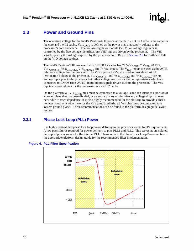
It is highly critical that phase lock loop power delivery to the processor meets Intel’s requirements. A low pass filter is required for power delivery to pins PLL1 and PLL2. This serves as an isolated, decoupled power source for the internal PLL. Please refer to the Phase Lock Loop Power section in the appropriate platform design guide for the recommended filter implementation.
Figure 4. PLL Filter Specification
10 Datasheet
Intel® Pentium® III Processor with 512KB L2 Cache at 1.13GHz to 1.40GHz
2.4 Decoupling Guidelines
Due to the large number of transistors and high internal clock speeds, the processor is capable of generating large average current swings between low and full power states. The fluctuations can cause voltages on power planes to sag below their nominal values if bulk decoupling is not adequate. Care must be taken in the board design to ensure that the voltage provided to the processor remains within the specifications listed in Table 7. Failure to do so can result in timing violations (in the event of a voltage sag) or a reduced lifetime of the component (in the event of a voltage overshoot).
2.4.1 Processor VCCCORE Decoupling
The regulator for the VCCCORE input must be capable of delivering the dICCCORE/dt (defined in Table 7) while maintaining the required tolerances (also defined in Table 7). Failure to meet these specifications can result in timing violations (during VCCCORE sag) or a reduced lifetime of the component (during VCCCORE overshoot).
The processor requires both high frequency and bulk decoupling on the system motherboard for proper AGTL bus operation. The minimum recommendation for the processor decoupling requirement is listed below. All capacitors should be placed next to and within the PGA370 socket cavity and mounted on the primary side of the motherboard. The capacitors are arranged to minimize the overall inductance between the VCCCORE and Vss power pins.
Decoupling Recommendations:
1) VCCCORE decoupling - A minimum of sixteen 4.7uF capacitors in a 1206 package.
2) VTT decoupling - Twenty 0.1uF capacitors in 0603 packages.
3) VREF decoupling - 0.1uF and 0.001uF capacitors in 0603 package placed near the VREF pins.
For additional decoupling requirements, please refer to the appropriate platform design guide for recommended capacitor component value/quantity and placement.
2.5 Processor System Bus Clock and Processor Clocking
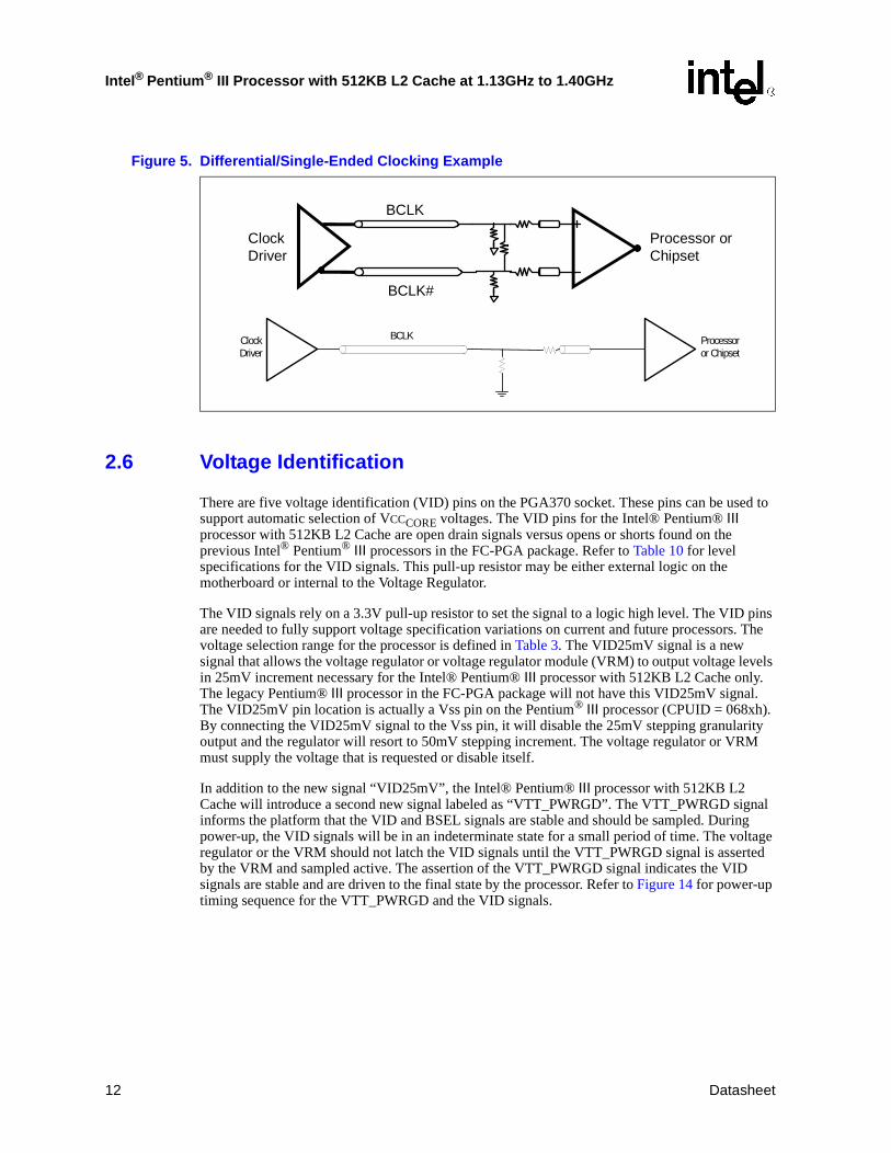
The Intel® Pentium® III processor with 512KB L2 Cache will implement an auto-detect mechanism that will allow the processor to use either single-ended or differential signaling for the system bus and processor clocking. The processor checks to see if the signal on pin Y33 is toggling. If this signal is toggling then the processor operates in differential mode. Refer to Figure 5 for an example on differential clocking. Resistor values and clock topology are listed in the appropriate platform design guide for a differential implementation. Note: References to BCLK throughout this document will also imply to it’s complement signal, BCLK# in differential implementations, and when noted otherwise.
The BCLK input directly controls the operating speed of the system bus interface. All AGTL system bus timing parameters are specified with respect to the crossing point of the rising edge of the BCLK and the falling edge of BCLK# inputs in a differential implementation. See the P6 Family of Processors Hardware Developer’s Manual for further details. The reference voltage of the BCLK in the P6 Family of Processors Hardware Developer Manual is re-defined as the crossing point of the BCLK and BCLK# in a differential implementation.
Datasheet 11
Intel® Pentium® III Processor with 512KB L2 Cache at 1.13GHz to 1.40GHz
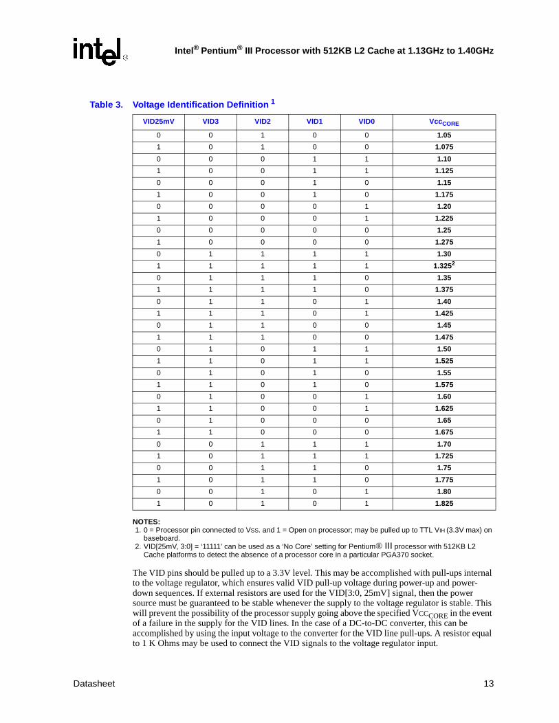
2.6 Voltage Identification
There are five voltage identification (VID) pins on the PGA370 socket. These pins can be used to support automatic selection of VCCCORE voltages. The VID pins for the Intel® Pentium® III processor with 512KB L2 Cache are open drain signals versus opens or shorts found on the previous Intel® Pentium® III processors in the FC-PGA package. Refer to Table 10 for level specifications for the VID signals. This pull-up resistor may be either external logic on the motherboard or internal to the Voltage Regulator.
The VID signals rely on a 3.3V pull-up resistor to set the signal to a logic high level. The VID pins are needed to fully support voltage specification variations on current and future processors. The voltage selection range for the processor is defined in Table 3. The VID25mV signal is a new signal that allows the voltage regulator or voltage regulator module (VRM) to output voltage levels in 25mV increment necessary for the Intel® Pentium® III processor with 512KB L2 Cache only. The legacy Pentium® III processor in the FC-PGA package will not have this VID25mV signal. The VID25mV pin location is actually a Vss pin on the Pentium® III processor (CPUID = 068xh). By connecting the VID25mV signal to the Vss pin, it will disable the 25mV stepping granularity output and the regulator will resort to 50mV stepping increment. The voltage regulator or VRM must supply the voltage that is requested or disable itself.
In addition to the new signal “VID25mV”, the Intel® Pentium® III processor with 512KB L2 Cache will introduce a second new signal labeled as “VTT_PWRGD”. The VTT_PWRGD signal informs the platform that the VID and BSEL signals are stable and should be sampled. During power-up, the VID signals will be in an indeterminate state for a small period of time. The voltage regulator or the VRM should not latch the VID signals until the VTT_PWRGD signal is asserted by the VRM and sampled active. The assertion of the VTT_PWRGD signal indicates the VID signals are stable and are driven to the final state by the processor. Refer to Figure 14 for power-up timing sequence for the VTT_PWRGD and the VID signals.
Figure 5. Differential/Single-Ended Clocking Example
BCLK
BCLK#
ClockDriver
Processor orChipset
ClockDriver
BCLK Processoror Chipset
12 Datasheet
Intel® Pentium® III Processor with 512KB L2 Cache at 1.13GHz to 1.40GHz
NOTES:1. 0 = Processor pin connected to VSS. and 1 = Open on processor; may be pulled up to TTL VIH (3.3V max) on
baseboard.2. VID[25mV, 3:0] = ‘11111’ can be used as a ‘No Core’ setting for Pentium® III processor with 512KB L2
Cache platforms to detect the absence of a processor core in a particular PGA370 socket.
The VID pins should be pulled up to a 3.3V level. This may be accomplished with pull-ups internal to the voltage regulator, which ensures valid VID pull-up voltage during power-up and power-down sequences. If external resistors are used for the VID[3:0, 25mV] signal, then the power source must be guaranteed to be stable whenever the supply to the voltage regulator is stable. This will prevent the possibility of the processor supply going above the specified VCCCORE in the event of a failure in the supply for the VID lines. In the case of a DC-to-DC converter, this can be accomplished by using the input voltage to the converter for the VID line pull-ups. A resistor equal to 1 K Ohms may be used to connect the VID signals to the voltage regulator input.
Table 3. Voltage Identification Definition 1
VID25mV VID3 VID2 VID1 VID0 VccCORE
0 0 1 0 0 1.05
1 0 1 0 0 1.075
0 0 0 1 1 1.10
1 0 0 1 1 1.125
0 0 0 1 0 1.15
1 0 0 1 0 1.175
0 0 0 0 1 1.20
1 0 0 0 1 1.225
0 0 0 0 0 1.25
1 0 0 0 0 1.275
0 1 1 1 1 1.30
1 1 1 1 1 1.3252
0 1 1 1 0 1.35
1 1 1 1 0 1.375
0 1 1 0 1 1.40
1 1 1 0 1 1.425
0 1 1 0 0 1.45
1 1 1 0 0 1.475
0 1 0 1 1 1.50
1 1 0 1 1 1.525
0 1 0 1 0 1.55
1 1 0 1 0 1.575
0 1 0 0 1 1.60
1 1 0 0 1 1.625
0 1 0 0 0 1.65
1 1 0 0 0 1.675
0 0 1 1 1 1.70
1 0 1 1 1 1.725
0 0 1 1 0 1.75
1 0 1 1 0 1.775
0 0 1 0 1 1.80
1 0 1 0 1 1.825
Datasheet 13
Intel® Pentium® III Processor with 512KB L2 Cache at 1.13GHz to 1.40GHz
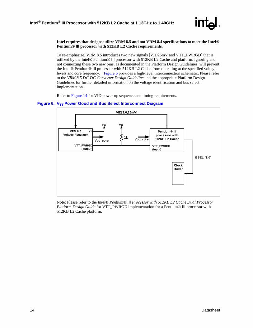
Intel requires that designs utilize VRM 8.5 and not VRM 8.4 specifications to meet the Intel® Pentium® III processor with 512KB L2 Cache requirements.
To re-emphasize, VRM 8.5 introduces two new signals [VID25mV and VTT_PWRGD] that is utilized by the Intel® Pentium® III processor with 512KB L2 Cache and platform. Ignoring and not connecting these two new pins, as documented in the Platform Design Guidelines, will prevent the Intel® Pentium® III processor with 512KB L2 Cache from operating at the specified voltage levels and core frequency. Figure 6 provides a high-level interconnection schematic. Please refer to the VRM 8.5 DC-DC Converter Design Guideline and the appropriate Platform Design Guidelines for further detailed information on the voltage identification and bus select implementation.
Refer to Figure 14 for VID power-up sequence and timing requirements.
Note: Please refer to the Intel® Pentium® III Processor with 512KB L2 Cache Dual Processor Platform Design Guide for VTT_PWRGD implementation for a Pentium® III processor with 512KB L2 Cache platform.
Figure 6. VTT Power Good and Bus Select Interconnect Diagram
VRM 8.5Voltage Regulator
Pentium® IIIprocessor with
512KB L2 Cache
ClockDriver
Vtt
VTT_PWRGD(output)
VTT_PWRGD(input)
Vtt
1k
Vtt
VID[3:0,25mV]
Vcc_core Vcc_core
BSEL [1:0]
14 Datasheet
Intel® Pentium® III Processor with 512KB L2 Cache at 1.13GHz to 1.40GHz
2.7 Processor System Bus Unused Pins
All RESERVED pins must remain unconnected unless specifically noted. Connection of these pins to VCCCORE, VREF, VSS, VTT or to any other signal (including each other) can result in component malfunction or incompatibility with future processors. See Section 5.4 for a pin listing of the processor and the location of each RESERVED pin.
PICCLK must be driven with a valid clock input and the PICD[1:0] signals must be pulled-up to VCCCMOS1.5 even when the APIC will not be used. A separate pull-up resistor must be provided for each PICD signal.
For reliable operation, always connect unused inputs or bidirectional signals to their deasserted signal level. The pull-up or pull-down resistor values are system dependent and should be chosen such that the logic high (VIH) and logic low (VIL) requirements are met. See Table 10 for level specifications of non-AGTL signals.
For unused AGTL inputs, the on-die termination will be sufficient. No external RTT is necessary on the motherboard
For unused CMOS inputs, active low signals should be connected through a pull-up resistor to VCCCMOS1.5 and meet VIH requirements. Unused active high CMOS inputs should be connected through a pull-down resistor to ground (VSS) and meet VIL requirements. Unused CMOS outputs can be left unconnected. A resistor must be used when tying bidirectional signals to power or ground. When tying any signal to power or ground, a resistor will also allow for system testability.
2.8 Processor System Bus Signal Groups
To simplify the following discussion, the processor system bus signals have been combined into groups by buffer type. All P6 family processor system bus outputs are open drain and require a high-level source provided termination resistors. However, the Intel® Pentium® III processor with 512KB L2 Cache includes on-die termination for AGTL signals and termination resistors placed on the platform are not necessary except for the RESET# signal which still requires external termination.
AGTL input signals have differential input buffers which use VREF as a reference signal. AGTL output signals require termination to 1.25 V. In this document, the term “AGTL Input” refers to the AGTL input group as well as the AGTL I/O group when receiving. Similarly, “AGTL Output” refers to the AGTL output group as well as the AGTL I/O group when driving.
The PWRGOOD signal input is a 1.8V signal level and must be pulled up to VCCCMOS1.8. The VTT_PWRGD is not 1.8V tolerant and must be connected to VTT (1.25V). Other CMOS inputs (A20M#, IGNNE#, INIT#, LINT0/INTR, LINT1/NMI, PREQ#, SMI, SLP#, and STPCLK#) are only 1.5 V tolerant and must be pulled up to VCCCMOS1.5. The CMOS, APIC, and TAP outputs are open drain and must be pulled to the appropriate level to meet the input specifications of the interfacing device.
The groups and the signals contained within each group are shown in Table 4. Refer to Section 7.0 for a description of these signals.
Datasheet 15
Intel® Pentium® III Processor with 512KB L2 Cache at 1.13GHz to 1.40GHz
NOTES:1. See Section 7.0 for information on the these signals.2. The BR0# pin is the only BREQ# signal that is bidirectional. See Section 7.0 for more information. 3. This signal is 1.25V.4. These signals are 1.5V.5. This signal is 1.8V.6. VCCCORE is the power supply for the processor core and is described in Section 2.6.
VID[3:0,25mV] is described in Section 2.6.VTT is used to terminate the system bus and generate VREF on the motherboard.VSS is system ground.BSEL[1:0] is described in Section 2.8.2 and Section 7.0.All other signals are described in Section 7.0.
7. This signal is used to control the value of the processor on-die termination resistance. Refer to the platform design guide for the recommended pulldown resistor value.
8. These signals are 3.3V.9. These signals are 2.0V.
10. 1.25V signal for Differential clock application and 2.5V for Single-ended clock application.
2.8.1 Asynchronous vs. Synchronous for System Bus Signals
All AGTL signals are synchronous to BCLK (BCLK/BCLK#). All of the CMOS, Clock, APIC, and TAP signals can be applied asynchronously to BCLK (BCLK/BCLK#). All APIC signals are synchronous to PICCLK. All TAP signals are synchronous to TCK.
Table 4. System Bus Signal Groups 1
Group Name Signals
AGTL Input BPRI#, DEFER#, RESET#, RSP#
AGTL Output PRDY#
AGTL I/OA[35:3]#, ADS#, AERR#, AP[1:0]#, BERR#, BINIT#, BNR#, BP[3:2]#, BPM[1:0]#, BR0#2, BR1#, D[63:0]#, DBSY#, DEP[7:0]#, DRDY#, HIT#, HITM#, LOCK#, REQ[4:0]#, RP#, RS[2:0]#, TRDY#
CMOS Input (1.25V)3 VTT_PWRGD
CMOS Input (1.5V)4
A20M#, FLUSH#, IGNNE#, INIT#, LINT0/INTR, LINT1/NMI, PREQ#, SLP#, SMI#, STPCLK#
CMOS Input (1.8V)5 PWRGOOD
CMOS Output
(1.5V)4FERR#, IERR#, THERMTRIP#
CMOS Output8
(3.3V)VID[3:0,25mV], BSEL[1:0]
System Bus Clock10
(1.25V/2.5V)BCLK0, BCLK0#
APIC Clock9 PICCLK
APIC I/O4 PICD[1:0]
TAP Input4 TCK, TDI, TMS, TRST#
TAP Output4 TDO
Power/Other6 CPUPRES#, DYN_OE, NCHTRL, PLL[2:1], SLEWCTRL, RTTCTRL7,THERMDN, THERMDP, VCCCORE, VREF, VSS, VTT, Reserved,
16 Datasheet

Intel® Pentium® III Processor with 512KB L2 Cache at 1.13GHz to 1.40GHz
2.8.2 System Bus Frequency Select Signals
The System Bus Frequency Select Signals (BSEL [1:0]) are used to select the system bus frequency for the Intel® Pentium® III processor. The BSEL signals are also used by the chipset and system bus clock generator. The BSEL pins for the Intel® Pentium® III processor with 512KB L2 Cache are open drain signals versus opens or shorts found on the previous Intel® Pentium® III processor in the FC-PGA package. Refer to Table 10 for level specifications for the BSEL signals.
The BSEL signals rely on a 3.3V pull-up resistor to set the signal to a logic high level. Similar to the VID signals described in Section 2.6, the VTT_PWRGD signal also informs the platform that the BSEL signals are stable and should be sampled. During power-up, the BSEL signals will be in an indeterminate state for a small period of time. The chipset or system bus clock generator should not sample and/or latch the BSEL signals until the VTT_PWRGD signal is asserted. The assertion of the VTT_PWRGD signal indicates the BSEL signals are stable and are driven to the final state by the processor. Refer to Figure 14 for power-up timing sequence for the VTT_PWRGD and the BSEL signals.
Table 5 defines the possible combinations of the BSEL signals and the frequency associated with each combination. The frequency selection is determined by the processor(s) and driven out to the chipset and system bus clock generator. All system bus agents must operate at the same frequency determined by the processor. The Intel® Pentium® III processor with 512KB L2 Cache operates at 133MHz system bus frequency based on the system bus specified rating marked on the package. Over or under-clocking the system bus frequency outside the specified rating marked on the package is not recommended.
Figure 7. BSEL[1:0] Example for a System Design
P r o c e s s o r
B S E L 0 B S E L 1
C h ip s e t
C lo c kD r i v e r
1 K o h mK o h m
3 . 3 V 3 . 3 V
Datasheet 17

Intel® Pentium® III Processor with 512KB L2 Cache at 1.13GHz to 1.40GHz
2.9 Maximum Ratings
Table 6 contains processor stress ratings only. Functional operation at the absolute maximum and minimum is not implied nor guaranteed. The processor should not receive a clock while subjected to these conditions. Functional operating conditions are given in the timing and level tables in Section 2.10 through Section 2.12. Extended exposure to the maximum ratings may affect device reliability. Furthermore, although the processor contains protective circuitry to resist damage from static electric discharge, one should always take precautions to avoid high static voltages or electric fields.
NOTES:1. Input voltage can never exceed VSS +1.78 volts.2. Input voltage can never exceed VSS + 2.08 volts.3. Input voltage can never go below -0.3V4. Parameter applies to CMOS, APIC, and TAP bus signal groups only.
2.10 Processor Voltage Level Specifications
The processor voltage level specifications in this section are defined at the PGA370 socket pins (bottom side of the motherboard). See Section 7.0 for the processor signal descriptions and Section 5.4 for the signal listings.
Most of the signals on the processor system bus are in the AGTL signal group. These signals are specified to be terminated to 1.25V. The voltage level specifications for these signals are listed in Table 9 on page 23.
To allow connection with other devices, the clock, CMOS, APIC, and TAP signals are designed to interface at non-AGTL levels. The voltage level specifications for these pins are listed in Table 10 on page 23.
Table 5. Frequency Select Truth Table for BSEL[1:0]
BSEL1 BSEL0 Frequency
0 0 Reserved
0 1 Reserved
1 0 Reserved
1 1 133 MHz
Table 6. Absolute Maximum Ratings
Symbol Parameter Min Max Unit Notes
TSTORAGE Processor storage temperature -40 85 °C
VCCCORE and
VTT Processor core voltage and termination supply voltage with respect to VSS
0.5 1.75 V
VinAGTL AGTL buffer input voltage -0.3 1.78 V 1, 3
VinCMOS1.5CMOS buffer DC input voltage with respect to VSS
-0.3 2.08 V 2, 3, 4
VVID & VBSEL Max VID and BSEL pin current -0.3 3.6 V
18 Datasheet

Intel® Pentium® III Processor with 512KB L2 Cache at 1.13GHz to 1.40GHz
Table 7 through Table 12 list the voltage level specifications for the Intel® Pentium® III processor with 512KB L2 Cache. Specifications are valid only while meeting specifications for junction temperature, clock frequency, and input voltages. Care should be taken to read all notes associated with each parameter.
NOTES:1. Unless otherwise noted, all specifications in this table apply to all processor frequencies.
Symbol Parameter Core Freq Min Typ Max Unit Notes
VCCCORE VCC for processor core
1.13GHz
1.26GHz
1.40GHz
1.45
1.45
1.45
V
V
V
3
VTT Static AGTL bus termination voltage 1.25 V 1.25 ±3%, 4
VTT Transient AGTL bus termination voltage 1.25 V 1.25 ±9%, 4
Vcc_cmos1.5 1.5 V 1.5 ± 10%, 12
Vcc_cmos1.8 1.8 V 1.8 ± 10%, 12
Baseboard VCCCORE Tolerance, Static
Processor core voltage static tolerance level at the PGA370 socket pins Please refer to Figure 8
and Table 8 for Tolerance values
V 5
Baseboard VCCCORE Tolerance, Transient
Processor core voltage transient tolerance level at the PGA370 socket pins
V 5
ICCCORE Icc for processor core
1.13 GHz
06B0
06B119.4 A
6
06B4 19.9 A
1.26 GHz
06B0
06B120.5 A
06B4 21.2 A
1.40 GHz
06B0
06B121.8 A
06B4 22.4 A
ICCCMOS1.5 ICC for VccCMOS1.5 250 mA
ICCCMOS1.8 ICC for VccCMOS1.8 1 mA
ICCCMOS3.3 ICC for VccCMOS3.3 35 mA
IVTTTermination voltage supply current 2.3 A
ISGntICC Stop-Grant for processor core
1.13GHz
1.26GHz
1.40GHz
13.2
14.0
14.8
A
A
A
7, 8
IDSLPICC Deep Sleep for processor core 10.2 A
dICCCORE/dt Power supply current slew rate
Please refer to Table 7 for Slew Rate
A/µs 8, 9, 10, 11
dIvTT/dt Termination current slew rate
Table 12
A/µs
8, 9, 10 See Table 12
Datasheet 19
Intel® Pentium® III Processor with 512KB L2 Cache at 1.13GHz to 1.40GHz
2. All specifications in this table apply only to the Intel® Pentium® III processor with 512KB L2 Cache. 3. VccCORE and IccCORE supply the processor core and the on-die L2 cache.4. VTT must be held to 1.25V ±9% while the AGTL bus is active. It is required that VTT be held to 1.25V ±3%
while the processor system bus is static (idle condition). The ±3% range is the required design target; ±9% will come from the transient noise added. This is measured at the PGA370 socket pins on the bottom side of the baseboard.
5. These are the tolerance requirements, across a 20 MHz frequency bandwidth, measured at the processor socket pin on the soldered-side of the motherboard. VCCCORE must return to within the static voltage specification within 100 µs after a transient event; see the VRM 8.5 DC-DC Converter Design Guidelines for further details.
6. Maximum ICC is measured at VCC typical voltage and under a maximum signal loading conditions.7. The current specified is also for AutoHALT state.8. Maximum values are specified by design/characterization at nominal VccCORE.9. Based on simulation and averaged over the duration of any change in current. Use to compute the maximum
inductance tolerable and reaction time of the voltage regulator. This parameter is not tested.10.dIcc/dt specifications are measured and specified at the PGA370 socket pins.11.Static voltage regulation includes: DC output initial voltage set point adjust, Output ripple and noise, Output
load ranges specified in the tables above. See VRM 8.5 DC-Dc Converter Design Guidelines.
20 Datasheet

Intel® Pentium® III Processor with 512KB L2 Cache at 1.13GHz to 1.40GHz
12.Pull ups only.
Table 7 contains typical slew rate data for the Intel® Pentium® III processor with 512KB L2 Cache. Actual slew rate values and wave-shapes may vary slightly depending on the type and size of decoupling capacitors used in a particular implementation
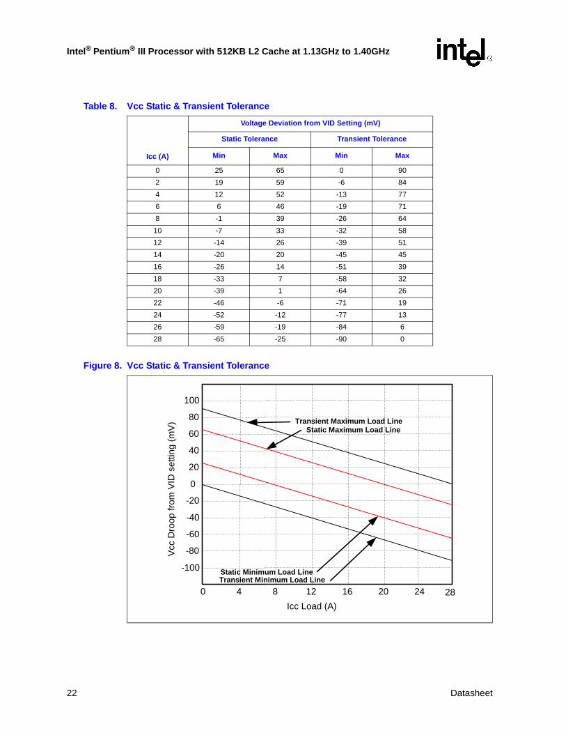
.Static minimum regulation requirements: VID set point +25mV - (3.214m.x Icc A)Static maximum regulation requirements: VID set point +65mV - (3.214m.x Icc A)Transient minimum regulation requirements: VID set point - (3.214m.x Icc A)Transient maximum regulation requirements: VID set point +90mV – (3.214m.x Icc A)
Table 7. Power Supply Current Slew Rate (dIcccore/dt)
Slew Rate – 26A Load Step
Slew Rate (26A) – ICC @ socket
0
5
10
15
20
25
30
0 1 2 3 4 5 6
Icc
@ s
ock
et (
A)
PW L Slew Rate Data Tim e (uS) Icc @ socket (A)
0.1 26.230.15 23.18
0.5 20.031 21.10
1.5 21.882 22.29
2.5 22.303 22.07
3.5 21.784 21.58
4.5 21.51
Datasheet 21
Intel® Pentium® III Processor with 512KB L2 Cache at 1.13GHz to 1.40GHz
Table 8. Vcc Static & Transient Tolerance
Icc (A)
Voltage Deviation from VID Setting (mV)
Static Tolerance Transient Tolerance
Min Max Min Max
0 25 65 0 90
2 19 59 -6 84
4 12 52 -13 77
6 6 46 -19 71
8 -1 39 -26 64
10 -7 33 -32 58
12 -14 26 -39 51
14 -20 20 -45 45
16 -26 14 -51 39
18 -33 7 -58 32
20 -39 1 -64 26
22 -46 -6 -71 19
24 -52 -12 -77 13
26 -59 -19 -84 6
28 -65 -25 -90 0
Figure 8. Vcc Static & Transient Tolerance
-20
-60
-40
-80
-100
0
20
40
60
80
0 4 8 12 16 20 24
Vcc
Dro
op fr
om V
ID s
ettin
g (m
V)
Icc Load (A)
100
Transient Maximum Load LineStatic Maximum Load Line
Transient Minimum Load LineStatic Minimum Load Line
28
22 Datasheet
Intel® Pentium® III Processor with 512KB L2 Cache at 1.13GHz to 1.40GHz
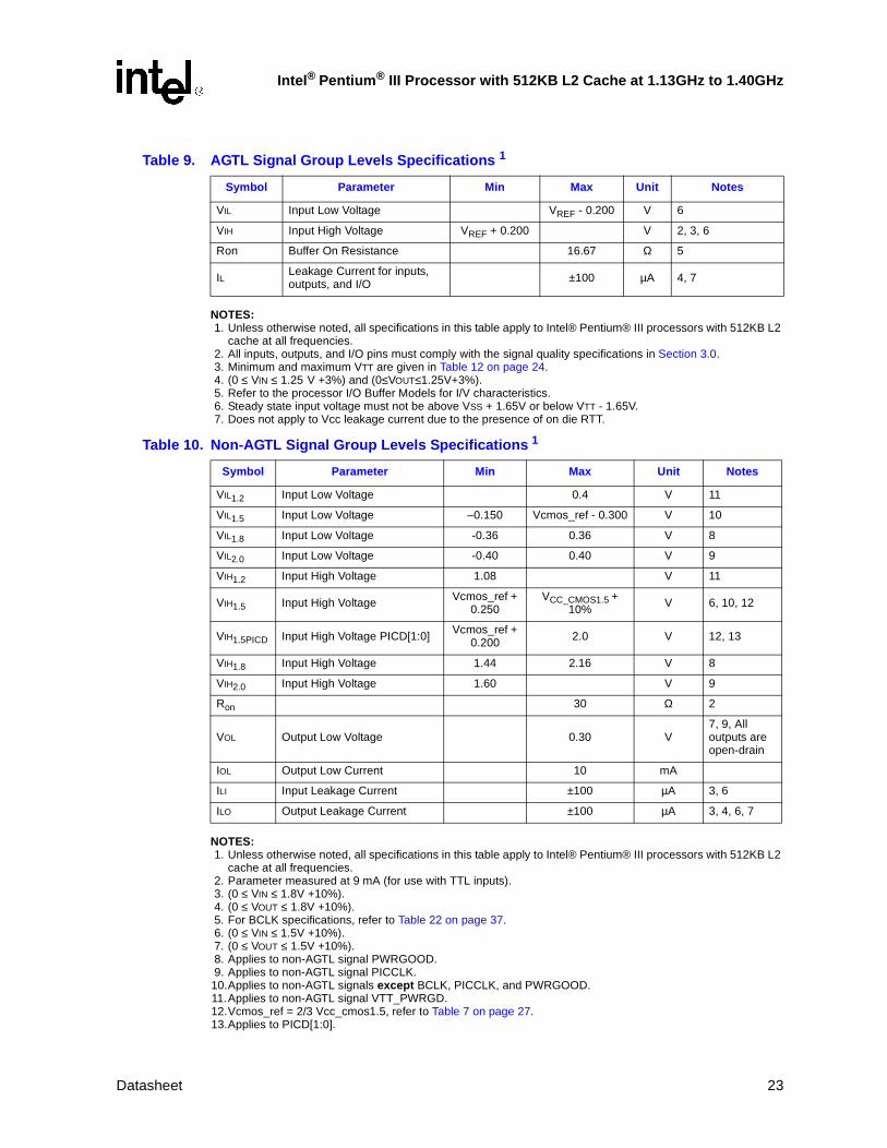
NOTES:1. Unless otherwise noted, all specifications in this table apply to Intel® Pentium® III processors with 512KB L2
cache at all frequencies.2. All inputs, outputs, and I/O pins must comply with the signal quality specifications in Section 3.0.3. Minimum and maximum VTT are given in Table 12 on page 24.4. (0 ≤ VIN ≤ 1.25 V +3%) and (0≤VOUT≤1.25V+3%).5. Refer to the processor I/O Buffer Models for I/V characteristics.6. Steady state input voltage must not be above VSS + 1.65V or below VTT - 1.65V.7. Does not apply to Vcc leakage current due to the presence of on die RTT.
NOTES:1. Unless otherwise noted, all specifications in this table apply to Intel® Pentium® III processors with 512KB L2
cache at all frequencies.2. Parameter measured at 9 mA (for use with TTL inputs).3. (0 ≤ VIN ≤ 1.8V +10%).4. (0 ≤ VOUT ≤ 1.8V +10%).5. For BCLK specifications, refer to Table 22 on page 37.6. (0 ≤ VIN ≤ 1.5V +10%).7. (0 ≤ VOUT ≤ 1.5V +10%). 8. Applies to non-AGTL signal PWRGOOD. 9. Applies to non-AGTL signal PICCLK.10.Applies to non-AGTL signals except BCLK, PICCLK, and PWRGOOD.11.Applies to non-AGTL signal VTT_PWRGD.12.Vcmos_ref = 2/3 Vcc_cmos1.5, refer to Table 7 on page 27.13.Applies to PICD[1:0].
Table 9. AGTL Signal Group Levels Specifications 1
Symbol Parameter Min Max Unit Notes
VIL Input Low Voltage VREF - 0.200 V 6
VIH Input High Voltage VREF + 0.200 V 2, 3, 6
Ron Buffer On Resistance 16.67 Ω 5
IL Leakage Current for inputs, outputs, and I/O ±100 µA 4, 7
Table 10. Non-AGTL Signal Group Levels Specifications 1
Symbol Parameter Min Max Unit Notes
VIL1.2 Input Low Voltage 0.4 V 11
VIL1.5 Input Low Voltage –0.150 Vcmos_ref - 0.300 V 10
VIL1.8 Input Low Voltage -0.36 0.36 V 8
VIL2.0 Input Low Voltage -0.40 0.40 V 9
VIH1.2 Input High Voltage 1.08 V 11
VIH1.5 Input High Voltage Vcmos_ref + 0.250
VCC_CMOS1.5 + 10% V 6, 10, 12
VIH1.5PICD Input High Voltage PICD[1:0] Vcmos_ref + 0.200 2.0 V 12, 13
VIH1.8 Input High Voltage 1.44 2.16 V 8
VIH2.0 Input High Voltage 1.60 V 9
Ron 30 Ω 2
VOL Output Low Voltage 0.30 V7, 9, All outputs are open-drain
IOL Output Low Current 10 mA
ILI Input Leakage Current ±100 µA 3, 6
ILO Output Leakage Current ±100 µA 3, 4, 6, 7
Datasheet 23
Intel® Pentium® III Processor with 512KB L2 Cache at 1.13GHz to 1.40GHz
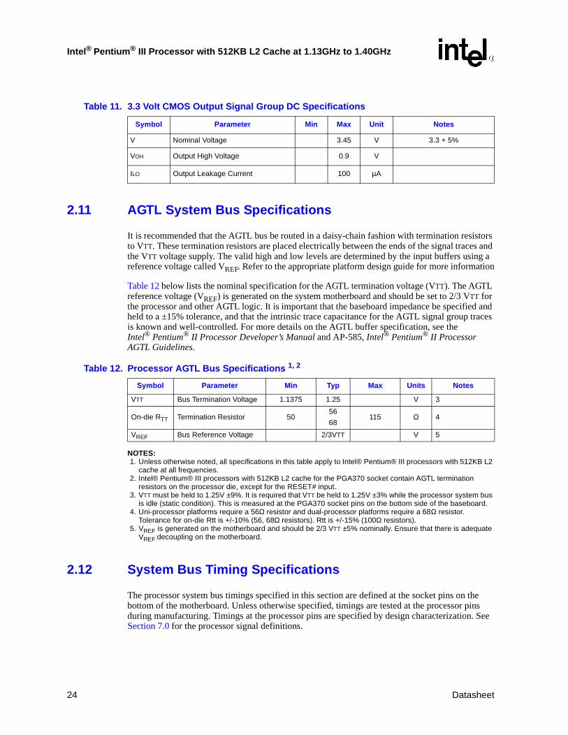
2.11 AGTL System Bus Specifications
It is recommended that the AGTL bus be routed in a daisy-chain fashion with termination resistors to VTT. These termination resistors are placed electrically between the ends of the signal traces and the VTT voltage supply. The valid high and low levels are determined by the input buffers using a reference voltage called VREF. Refer to the appropriate platform design guide for more information
Table 12 below lists the nominal specification for the AGTL termination voltage (VTT). The AGTL reference voltage (VREF) is generated on the system motherboard and should be set to 2/3 VTT for the processor and other AGTL logic. It is important that the baseboard impedance be specified and held to a ±15% tolerance, and that the intrinsic trace capacitance for the AGTL signal group traces is known and well-controlled. For more details on the AGTL buffer specification, see the Intel® Pentium® II Processor Developer’s Manual and AP-585, Intel® Pentium® II Processor AGTL Guidelines.
NOTES:1. Unless otherwise noted, all specifications in this table apply to Intel® Pentium® III processors with 512KB L2
cache at all frequencies.2. Intel® Pentium® III processors with 512KB L2 cache for the PGA370 socket contain AGTL termination
resistors on the processor die, except for the RESET# input.3. VTT must be held to 1.25V ±9%. It is required that VTT be held to 1.25V ±3% while the processor system bus
is idle (static condition). This is measured at the PGA370 socket pins on the bottom side of the baseboard.4. Uni-processor platforms require a 56Ω resistor and dual-processor platforms require a 68Ω resistor.
Tolerance for on-die Rtt is +/-10% (56, 68Ω resistors). Rtt is +/-15% (100Ω resistors).5. VREF is generated on the motherboard and should be 2/3 VTT ±5% nominally. Ensure that there is adequate
VREF decoupling on the motherboard.
2.12 System Bus Timing Specifications
The processor system bus timings specified in this section are defined at the socket pins on the bottom of the motherboard. Unless otherwise specified, timings are tested at the processor pins during manufacturing. Timings at the processor pins are specified by design characterization. See Section 7.0 for the processor signal definitions.
Table 11. 3.3 Volt CMOS Output Signal Group DC Specifications
Symbol Parameter Min Max Unit Notes
V Nominal Voltage 3.45 V 3.3 + 5%
VOH Output High Voltage 0.9 V
ILO Output Leakage Current 100 µA
Table 12. Processor AGTL Bus Specifications 1, 2
Symbol Parameter Min Typ Max Units Notes
VTT Bus Termination Voltage 1.1375 1.25 V 3
On-die RTT Termination Resistor 5056
68115 Ω 4
VREF Bus Reference Voltage 2/3VTT V 5
24 Datasheet

Intel® Pentium® III Processor with 512KB L2 Cache at 1.13GHz to 1.40GHz
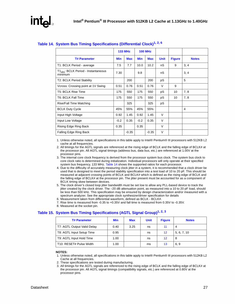
Table 13 through Table 19 list the timing specifications associated with the processor system bus. These specifications are divided into the following categories: Table 13 contains the system bus clock specifications for single-ended clock mode operation and Table 14 contains the system bus clock specifications for differential clock mode operation. Table 15 contains the AGTL specifications, Table 16 contains the CMOS signal group specifications, Table 17 contains timings for the reset conditions, Table 18 and covers APIC bus timing, and Table 19 covers TAP timing.
All processor system bus timing specifications for the AGTL signal group are relative to the rising edge of the BCLK input. All AGTL timings are referenced to VREF for both ‘0’ and ‘1’ logic levels unless otherwise specified.
The timings specified in this section should be used in conjunction with the I/O buffer models provided by Intel. These I/O buffer models, which include package information, are available for the Intel® Pentium® III processor with 512KB L2 Cache in the FC-PGA2 package in IBIS* 3.1 model format. These I/O buffer models are available at Intel’s Developer Website (http://developer.intel.com).
AGTL layout guidelines are also available in the appropriate platform design guide.Care should be taken to read all notes associated with a particular timing parameter.
Datasheet 25
Intel® Pentium® III Processor with 512KB L2 Cache at 1.13GHz to 1.40GHz
7
NOTES:1. Unless otherwise noted, all specifications in this table apply to Intel® Pentium® III processors with 512KB L2
cache at all frequencies.2. Period, jitter, offset and skew measured at 1.25V.3. Measured from 0.5 to 2.0V.4. CLKREF (BCLK#) = 1.25V with +/- 5% DC tolerance. CLKREF must be generated from a stable source. AC
tolerances must be less than -40dB @ 1MHz. 5. BCLK High Time is measured above 2.0V.6. BCLK Low Time is measured below 0.5V.
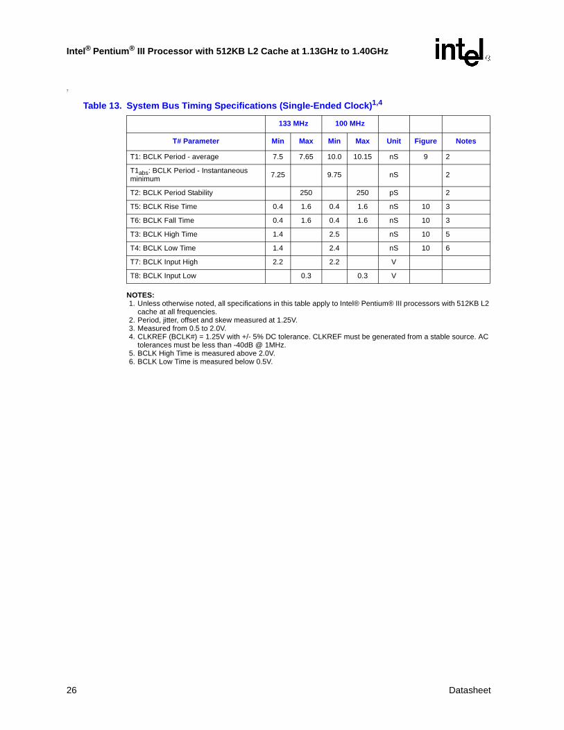
Table 13. System Bus Timing Specifications (Single-Ended Clock)1,4
133 MHz 100 MHz
T# Parameter Min Max Min Max Unit Figure Notes
T1: BCLK Period - average 7.5 7.65 10.0 10.15 nS 9 2
T1abs: BCLK Period - Instantaneous minimum 7.25 9.75 nS 2
T2: BCLK Period Stability 250 250 pS 2
T5: BCLK Rise Time 0.4 1.6 0.4 1.6 nS 10 3
T6: BCLK Fall Time 0.4 1.6 0.4 1.6 nS 10 3
T3: BCLK High Time 1.4 2.5 nS 10 5
T4: BCLK Low Time 1.4 2.4 nS 10 6
T7: BCLK Input High 2.2 2.2 V
T8: BCLK Input Low 0.3 0.3 V
26 Datasheet
Intel® Pentium® III Processor with 512KB L2 Cache at 1.13GHz to 1.40GHz
1. Unless otherwise noted, all specifications in this table apply to Intel® Pentium® III processors with 512KB L2 cache at all frequencies.
2. All timings for the AGTL signals are referenced at the rising edge of BCLK and the falling edge of BCLK# at the processor pin. All AGTL signal timings (address bus, data bus, etc.) are referenced at 1.00V at the processor pins.
3. The internal core clock frequency is derived from the processor system bus clock. The system bus clock to core clock ratio is determined during initialization. Individual processors will only operate at their specified system bus frequency, 133 MHz. Table 14 shows the supported ratios for each processor.
4. Due to the difficulty of accurately measuring clock jitter in a system, it is recommended that a clock driver be used that is designed to meet the period stability specification into a test load of 10 to 20 pF. This should be measured at adjacent crossing points of BCLK and BCLK# which is defined as the rising edge of BCLK and the falling edge of BCLK# at the processor pin. The jitter present must be accounted for as a component of BCLK timing skew between devices.
5. The clock driver’s closed loop jitter bandwidth must be set low to allow any PLL-based device to track the jitter created by the clock driver. The –20 dB attenuation point, as measured into a 10 to 20 pF load, should be less than 500 kHz. This specification may be ensured by design characterization and/or measured with a spectrum analyzer. See the appropriate clock synthesizer/driver specification for details
6. Measurement taken from differential waveform, defined as BCLK - BCLK#.7. Rise time is measured from -0.35 to +0.35V and fall time is measured from 0.35V to -0.35V.8. Measured at the socket pin.
NOTES:1. Unless otherwise noted, all specifications in this table apply to Intel® Pentium® III processors with 512KB L2
Cache at all frequencies.2. These specifications are tested during manufacturing.3. All timings for the AGTL signals are referenced to the rising edge of BCLK and the falling edge of BCLK# at
the processor pin. All AGTL signal timings (compatibility signals, etc.) are referenced at 0.80V at the processor pins.
Table 14. System Bus Timing Specifications (Differential Clock)1, 2, 6
133 MHz 100 MHz
T# Parameter Min Max Min Max Unit Figure Notes
T1: BCLK Period - average 7.5 7.7 10.0 10.2 nS 9 3, 4
T1abs: BCLK Period - Instantaneous minimum 7.30 9.8 nS 3, 4
T2: BCLK Period Stability 200 200 pS 5
Vcross: Crossing point at 1V Swing 0.51 0.76 0.51 0.76 V 9
T5: BCLK Rise Time 175 550 175 550 pS 10 7, 8
T6: BCLK Fall Time 175 550 175 550 pS 10 7, 8
Rise/Fall Time Matching 325 325 pS
BCLK Duty Cycle 45% 55% 45% 55% 4
Input High Voltage 0.92 1.45 0.92 1.45 V
Input Low Voltage -0.2 0.35 -0.2 0.35 V
Rising Edge Ring Back 0.35 0.35 V
Falling Edge Ring Back -0.35 -0.35 V
Table 15. System Bus Timing Specifications (AGTL Signal Group)1, 2, 3
T# Parameter Min Max Unit Figure Notes
T7: AGTL Output Valid Delay 0.40 3.25 ns 11 4
T8: AGTL Input Setup Time 0.95 ns 12 5, 6, 7, 10
T9: AGTL Input Hold Time 1.00 ns 12 8
T10: RESET# Pulse Width 1.00 ms 13 6, 9
Datasheet 27
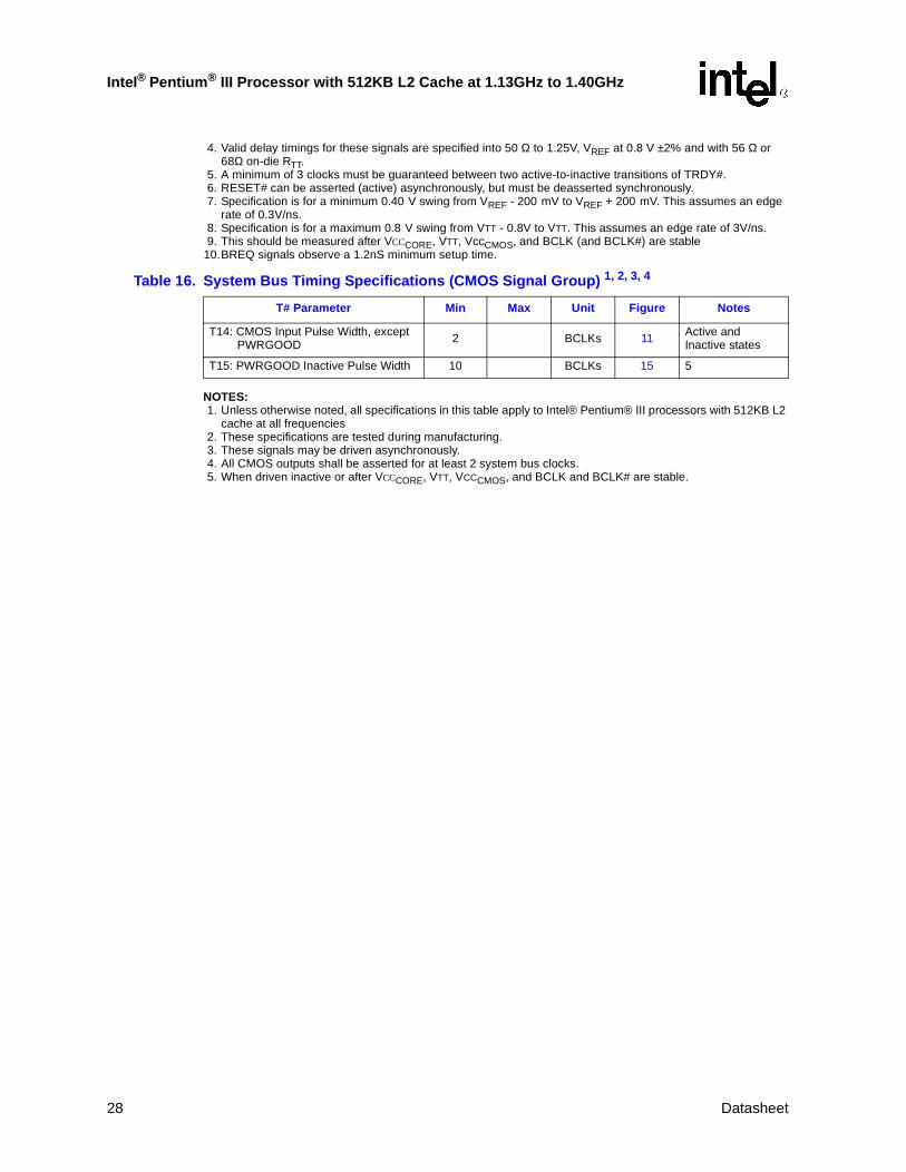
Intel® Pentium® III Processor with 512KB L2 Cache at 1.13GHz to 1.40GHz
4. Valid delay timings for these signals are specified into 50 Ω to 1.25V, VREF at 0.8 V ±2% and with 56 Ω or 68Ω on-die RTT.
5. A minimum of 3 clocks must be guaranteed between two active-to-inactive transitions of TRDY#.6. RESET# can be asserted (active) asynchronously, but must be deasserted synchronously. 7. Specification is for a minimum 0.40 V swing from VREF - 200 mV to VREF + 200 mV. This assumes an edge
rate of 0.3V/ns.8. Specification is for a maximum 0.8 V swing from VTT - 0.8V to VTT. This assumes an edge rate of 3V/ns.9. This should be measured after VCCCORE, VTT, VccCMOS, and BCLK (and BCLK#) are stable
10.BREQ signals observe a 1.2nS minimum setup time.
NOTES:1. Unless otherwise noted, all specifications in this table apply to Intel® Pentium® III processors with 512KB L2
cache at all frequencies2. These specifications are tested during manufacturing.3. These signals may be driven asynchronously. 4. All CMOS outputs shall be asserted for at least 2 system bus clocks.5. When driven inactive or after VCCCORE, VTT, VCCCMOS, and BCLK and BCLK# are stable.
Table 16. System Bus Timing Specifications (CMOS Signal Group) 1, 2, 3, 4
T# Parameter Min Max Unit Figure Notes
T14: CMOS Input Pulse Width, except PWRGOOD 2 BCLKs 11 Active and
Inactive states
T15: PWRGOOD Inactive Pulse Width 10 BCLKs 15 5
28 Datasheet

Intel® Pentium® III Processor with 512KB L2 Cache at 1.13GHz to 1.40GHz
NOTE:1. Unless otherwise noted, all specifications in this table apply to Intel® Pentium® III processors with 512KB L2
cache frequencies.
NOTES:1. Unless otherwise noted, all specifications in this table apply to Intel® Pentium® III processors with 512KB L2
cache at all frequencies.2. These specifications are tested during manufacturing.3. All timings for the APIC I/O signals are referenced to the PICCLK rising edge at 0.9 V at the processor pins.
All APIC I/O signal timings are referenced at 1.0 V at the processor pins.4. Referenced to PICCLK rising edge.5. For open drain signals, valid delay is synonymous with float delay.6. Valid delay timings for these signals are specified into 150 Ω load pulled up to 1.5 V.
Table 17. System Bus Timing Specifications (Reset Conditions) 1
T# Parameter Min Max Unit Figure Notes
T16: Reset Configuration Signals (A[14:5]#, BR0#, INIT#) Setup Time 4 BCLKs 13 Before deassertion
of RESET#
T17: Reset Configuration Signals (A[14:5]#, BR0#, INIT#) Hold Time 2 20 BCLKs 13 After clock that
deasserts RESET#
Table 18. System Bus Timing Specifications (APIC Clock and APIC I/O)1, 2, 3
T# Parameter Min Max Unit Figure Notes
T21: PICCLK Frequency 2.0 33.3 MHz
T22: PICCLK Period 30.0 500.0 ns 10
T23: PICCLK High Time 10.5 ns 10 @ > 1.60V
T24: PICCLK Low Time 10.5 ns 10 @ < 0.40V
T25: PICCLK Rise Time 0.25 3.0 ns 10 (0.40V - 1.60V)
T26: PICCLK Fall Time 0.25 3.0 ns 10 (1.60 - 0.40V)
T27: PICD[1:0] Setup Time 8.0 ns 12 4
T28: PICD[1:0] Hold Time 2.5 ns 12 4
T29a: PICD[1:0] Valid Delay (Rising Edge) 1.5 8.7 ns 11 4, 5, 6
T29b: PICD[1:0] Valid Delay (Falling Edge) 1.5 12.0 ns 10 4, 5, 6
Datasheet 29
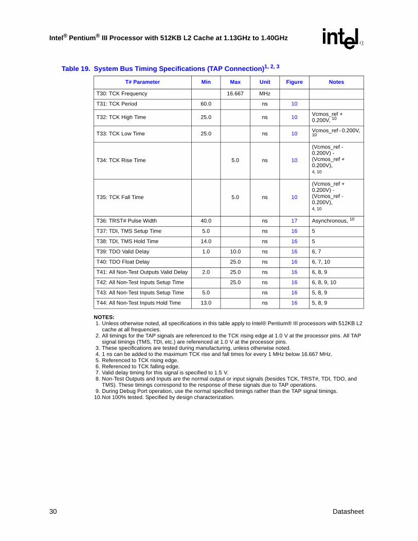
Intel® Pentium® III Processor with 512KB L2 Cache at 1.13GHz to 1.40GHz
NOTES:1. Unless otherwise noted, all specifications in this table apply to Intel® Pentium® III processors with 512KB L2
cache at all frequencies.2. All timings for the TAP signals are referenced to the TCK rising edge at 1.0 V at the processor pins. All TAP
signal timings (TMS, TDI, etc.) are referenced at 1.0 V at the processor pins.3. These specifications are tested during manufacturing, unless otherwise noted.4. 1 ns can be added to the maximum TCK rise and fall times for every 1 MHz below 16.667 MHz.5. Referenced to TCK rising edge.6. Referenced to TCK falling edge.7. Valid delay timing for this signal is specified to 1.5 V.8. Non-Test Outputs and Inputs are the normal output or input signals (besides TCK, TRST#, TDI, TDO, and
TMS). These timings correspond to the response of these signals due to TAP operations.9. During Debug Port operation, use the normal specified timings rather than the TAP signal timings.
10.Not 100% tested. Specified by design characterization.
Table 19. System Bus Timing Specifications (TAP Connection)1, 2, 3
T# Parameter Min Max Unit Figure Notes
T30: TCK Frequency 16.667 MHz
T31: TCK Period 60.0 ns 10
T32: TCK High Time 25.0 ns 10 Vcmos_ref + 0.200V, 10
T33: TCK Low Time 25.0 ns 10 Vcmos_ref - 0.200V, 10
T34: TCK Rise Time 5.0 ns 10
(Vcmos_ref - 0.200V) - (Vcmos_ref + 0.200V), 4, 10
T35: TCK Fall Time 5.0 ns 10
(Vcmos_ref + 0.200V) - (Vcmos_ref - 0.200V), 4, 10
T36: TRST# Pulse Width 40.0 ns 17 Asynchronous, 10
T37: TDI, TMS Setup Time 5.0 ns 16 5
T38: TDI, TMS Hold Time 14.0 ns 16 5
T39: TDO Valid Delay 1.0 10.0 ns 16 6, 7
T40: TDO Float Delay 25.0 ns 16 6, 7, 10
T41: All Non-Test Outputs Valid Delay 2.0 25.0 ns 16 6, 8, 9
T42: All Non-Test Inputs Setup Time 25.0 ns 16 6, 8, 9, 10
T43: All Non-Test Inputs Setup Time 5.0 ns 16 5, 8, 9
T44: All Non-Test Inputs Hold Time 13.0 ns 16 5, 8, 9
30 Datasheet
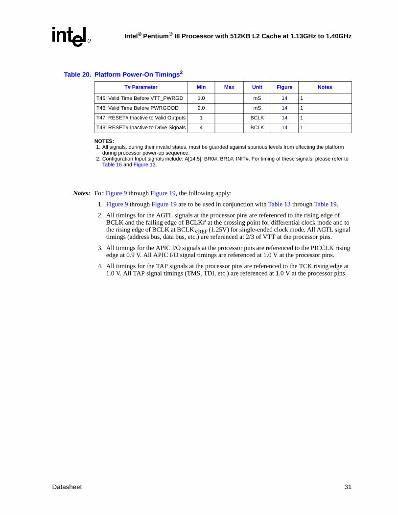
Intel® Pentium® III Processor with 512KB L2 Cache at 1.13GHz to 1.40GHz
NOTES:1. All signals, during their invalid states, must be guarded against spurious levels from effecting the platform
during processor power-up sequence.2. Configuration Input signals include: A[14:5], BR0#, BR1#, INIT#. For timing of these signals, please refer to
Table 16 and Figure 13.
Notes: For Figure 9 through Figure 19, the following apply:
1. Figure 9 through Figure 19 are to be used in conjunction with Table 13 through Table 19.
2. All timings for the AGTL signals at the processor pins are referenced to the rising edge of BCLK and the falling edge of BCLK# at the crossing point for differential clock mode and to the rising edge of BCLK at BCLKVREF (1.25V) for single-ended clock mode. All AGTL signal timings (address bus, data bus, etc.) are referenced at 2/3 of VTT at the processor pins.
3. All timings for the APIC I/O signals at the processor pins are referenced to the PICCLK rising edge at 0.9 V. All APIC I/O signal timings are referenced at 1.0 V at the processor pins.
4. All timings for the TAP signals at the processor pins are referenced to the TCK rising edge at 1.0 V. All TAP signal timings (TMS, TDI, etc.) are referenced at 1.0 V at the processor pins.
Table 20. Platform Power-On Timings2
T# Parameter Min Max Unit Figure Notes
T45: Valid Time Before VTT_PWRGD 1.0 mS 14 1
T46: Valid Time Before PWRGOOD 2.0 mS 14 1
T47: RESET# Inactive to Valid Outputs 1 BCLK 14 1
T48: RESET# Inactive to Drive Signals 4 BCLK 14 1
Datasheet 31
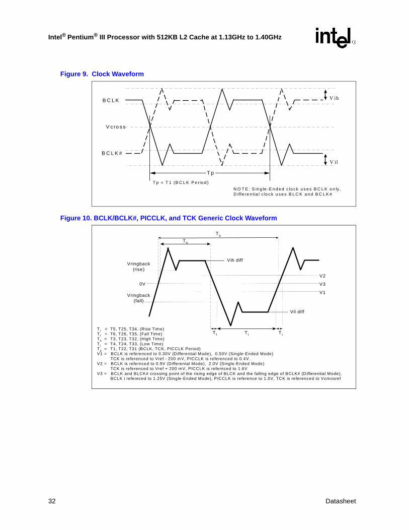
Intel® Pentium® III Processor with 512KB L2 Cache at 1.13GHz to 1.40GHz
Figure 9. Clock Waveform
Figure 10. BCLK/BCLK#, PICCLK, and TCK Generic Clock Waveform
V ih
B C L K #
B C L K
V il
V c ro s s
T p
T p = T 1 (B C L K P e r io d )
N O T E : S in g le -E n d e d c lo c k u s e s B C L K o n ly ,D if fe re n tia l c lo c k u s e s B L C K a n d B C L K #
V3
V1
V2
Tp
T l
Th
TrT f
Vringback(rise)
Vringback(fall)
Tr = T5, T25, T34, (Rise Time)Tf = T6, T26, T35, (Fall Time)Th = T3, T23, T32, (High Time)Tl = T4, T24, T33, (Low Time)Tp = T1, T22, T31 (BCLK, TCK, PICCLK Period)V1 = BCLK is referenced to 0.30V (Differential Mode), 0.50V (Single-Ended Mode)
TCK is referenced to Vref - 200 mV, PICCLK is referenced to 0.4V.V2 = BCLK is refernced to 0.9V (Differental Mode), 2.0V (Single-Ended Mode)
TCK is referenced to Vref + 200 mV, PICCLK is refernced to 1.6VV3 = BCLK and BLCK# crossing point of the rising edge of BLCK and the falling edge of BCLK# (Differential Mode),
BCLK i refereced to 1.25V (Single-Ended Mode), PICCLK is reference to 1.0V, TCK is referenced to Vcmosref
0V
Vih diff
Vil diff
32 Datasheet
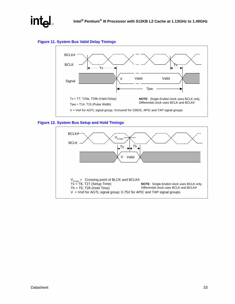
Intel® Pentium® III Processor with 512KB L2 Cache at 1.13GHz to 1.40GHz
Figure 11. System Bus Valid Delay Timings
Figure 12. System Bus Setup and Hold Timings
BCLK
SignalValid
Tx
V
Tx
Tpw
Tx = T7, T29a, T29b (Valid Delay)
Tpw = T14, T15 (Pulse Width)
V = Vref for AGTL signal group; Vcmosref for CMOS, APIC and TAP signal groups
BCLK#
Valid
NOTE: Single-Ended clock uses BCLK only,Differential clock uses BCLK and BCLK#
BCLK
Valid
Ts
V
Th
VCross = Crossing point of BLCK and BCLK#Ts = T8, T27 (Setup Time)Th = T9, T28 (Hold Time)V = Vref for AGTL signal group; 0.75V for APIC and TAP signal groups
VCross
BCLK#
NOTE: Single-Ended clock uses BCLK only,Differential clock uses BCLK and BCLK#
Datasheet 33
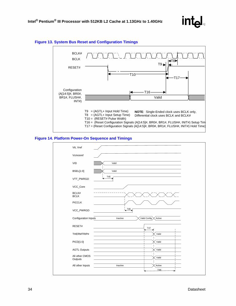
Intel® Pentium® III Processor with 512KB L2 Cache at 1.13GHz to 1.40GHz
Figure 13. System Bus Reset and Configuration Timings
Figure 14. Platform Power-On Sequence and Timings
T9 = (AGTL+ Input Hold Time)T8 = (AGTL+ Input Setup Time)T10 = (RESET# Pulse Width)T16 = (Reset Configuration Signals (A[14:5]#, BR0#, BR1#, FLUSH#, INIT#) Setup TimT17 = (Reset Configuration Signals (A[14:5]#, BR0#, BR1#, FLUSH#, INIT#) Hold Time)
BCLK
RESET#
Configuration(A[14:5]#, BR0#,BR1#, FLUSH#,
INT#)
BCLK#
Valid
T10
T16
T17
T8T9
NOTE: Single-Ended clock uses BCLK only,Differential clock uses BCLK and BCLK#
Vtt, Vref
Vcmosref
Valid
Valid
VID
BSEL[1:0]
T45VTT_PWRGD
VCC_Core
PICCLK
BCLK#BCLK
Valid Config ActiveInactive
Valid
Valid
Valid
Valid
Active
T46
T47
T48
VCC_PWRGD
Configuration Inputs
RESET#
THERMTRIP#
PICD[1:0]
AGTL Outputs
All other CMOSOutputs
InactiveAll other Inputs
34 Datasheet
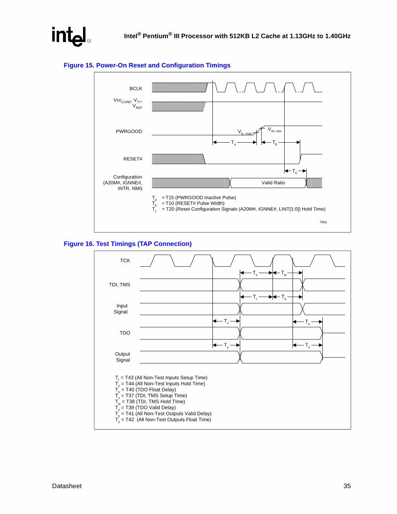
Intel® Pentium® III Processor with 512KB L2 Cache at 1.13GHz to 1.40GHz
Figure 15. Power-On Reset and Configuration Timings
Figure 16. Test Timings (TAP Connection)
Ta
Valid Ratio
TC
Tb
PWRGOOD
RESET#
Configuration(A20M#, IGNNE#,
INTR, NMI)
Ta = T15 (PWRGOOD Inactive Pulse)Tb = T10 (RESET# Pulse Width)Tc = T20 (Reset Configuration Signals (A20M#, IGNNE#, LINT[1:0]) Hold Time)
765a
BCLK
VIL, maxVIH, min
VccCORE, VTT,VREF
Tr = T43 (All Non-Test Inputs Setup Time)Ts = T44 (All Non-Test Inputs Hold Time)Tu = T40 (TDO Float Delay)Tv = T37 (TDI, TMS Setup Time)Tw = T38 (TDI, TMS Hold TIme)Tx = T39 (TDO Valid Delay)Ty = T41 (All Non-Test Outputs Valid Delay)Tz = T42 (All Non-Test Outputs Float Time)
Tv Tw
Tr Ts
Tu
Tz
Tx
Ty
TCK
TDI, TMS
InputSignal
TDO
OutputSignal
Datasheet 35
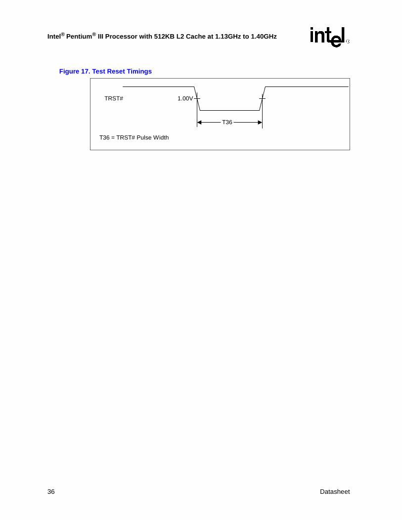
Intel® Pentium® III Processor with 512KB L2 Cache at 1.13GHz to 1.40GHz
Figure 17. Test Reset Timings
T36
TRST#
T36 = TRST# Pulse Width
1.00V
36 Datasheet
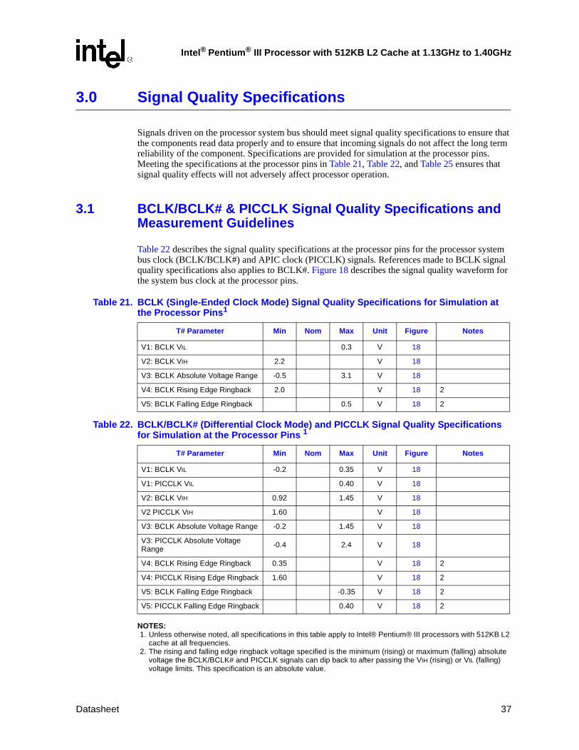
Intel® Pentium® III Processor with 512KB L2 Cache at 1.13GHz to 1.40GHz
3.0 Signal Quality Specifications
Signals driven on the processor system bus should meet signal quality specifications to ensure that the components read data properly and to ensure that incoming signals do not affect the long term reliability of the component. Specifications are provided for simulation at the processor pins. Meeting the specifications at the processor pins in Table 21, Table 22, and Table 25 ensures that signal quality effects will not adversely affect processor operation.
3.1 BCLK/BCLK# & PICCLK Signal Quality Specifications and Measurement Guidelines
Table 22 describes the signal quality specifications at the processor pins for the processor system bus clock (BCLK/BCLK#) and APIC clock (PICCLK) signals. References made to BCLK signal quality specifications also applies to BCLK#. Figure 18 describes the signal quality waveform for the system bus clock at the processor pins.
NOTES:1. Unless otherwise noted, all specifications in this table apply to Intel® Pentium® III processors with 512KB L2
cache at all frequencies.2. The rising and falling edge ringback voltage specified is the minimum (rising) or maximum (falling) absolute
voltage the BCLK/BCLK# and PICCLK signals can dip back to after passing the VIH (rising) or VIL (falling) voltage limits. This specification is an absolute value.
Table 21. BCLK (Single-Ended Clock Mode) Signal Quality Specifications for Simulation at the Processor Pins1
T# Parameter Min Nom Max Unit Figure Notes
V1: BCLK VIL 0.3 V 18
V2: BCLK VIH 2.2 V 18
V3: BCLK Absolute Voltage Range -0.5 3.1 V 18
V4: BCLK Rising Edge Ringback 2.0 V 18 2
V5: BCLK Falling Edge Ringback 0.5 V 18 2
Table 22. BCLK/BCLK# (Differential Clock Mode) and PICCLK Signal Quality Specifications for Simulation at the Processor Pins 1
T# Parameter Min Nom Max Unit Figure Notes
V1: BCLK VIL -0.2 0.35 V 18
V1: PICCLK VIL 0.40 V 18
V2: BCLK VIH 0.92 1.45 V 18
V2 PICCLK VIH 1.60 V 18
V3: BCLK Absolute Voltage Range -0.2 1.45 V 18
V3: PICCLK Absolute Voltage Range -0.4 2.4 V 18
V4: BCLK Rising Edge Ringback 0.35 V 18 2
V4: PICCLK Rising Edge Ringback 1.60 V 18 2
V5: BCLK Falling Edge Ringback -0.35 V 18 2
V5: PICCLK Falling Edge Ringback 0.40 V 18 2
Datasheet 37
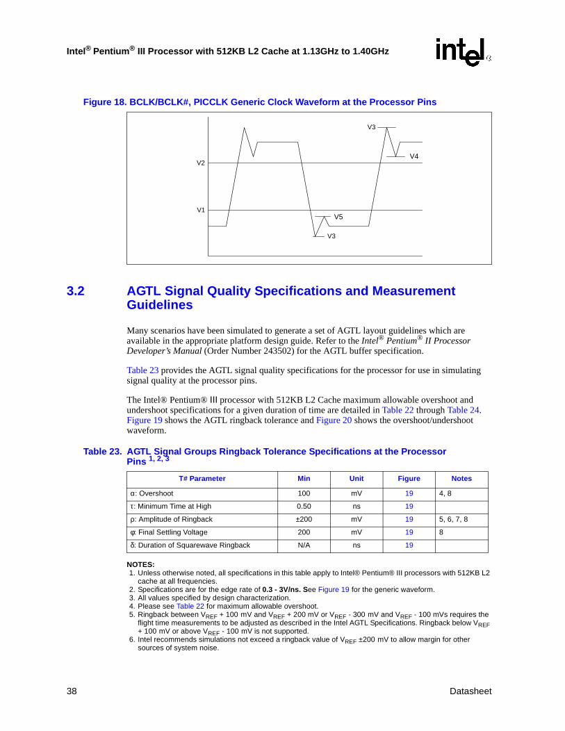
Intel® Pentium® III Processor with 512KB L2 Cache at 1.13GHz to 1.40GHz
3.2 AGTL Signal Quality Specifications and Measurement Guidelines
Many scenarios have been simulated to generate a set of AGTL layout guidelines which are available in the appropriate platform design guide. Refer to the Intel® Pentium® II Processor Developer’s Manual (Order Number 243502) for the AGTL buffer specification.
Table 23 provides the AGTL signal quality specifications for the processor for use in simulating signal quality at the processor pins.
The Intel® Pentium® III processor with 512KB L2 Cache maximum allowable overshoot and undershoot specifications for a given duration of time are detailed in Table 22 through Table 24. Figure 19 shows the AGTL ringback tolerance and Figure 20 shows the overshoot/undershoot waveform.
NOTES:1. Unless otherwise noted, all specifications in this table apply to Intel® Pentium® III processors with 512KB L2
cache at all frequencies.2. Specifications are for the edge rate of 0.3 - 3V/ns. See Figure 19 for the generic waveform.3. All values specified by design characterization.4. Please see Table 22 for maximum allowable overshoot.5. Ringback between VREF + 100 mV and VREF + 200 mV or VREF - 300 mV and VREF - 100 mVs requires the
flight time measurements to be adjusted as described in the Intel AGTL Specifications. Ringback below VREF + 100 mV or above VREF - 100 mV is not supported.
6. Intel recommends simulations not exceed a ringback value of VREF ±200 mV to allow margin for other sources of system noise.
Figure 18. BCLK/BCLK#, PICCLK Generic Clock Waveform at the Processor Pins
V2
V1
V3
V3
V4
V5
Table 23. AGTL Signal Groups Ringback Tolerance Specifications at the Processor Pins 1, 2, 3
T# Parameter Min Unit Figure Notes
α: Overshoot 100 mV 19 4, 8
τ: Minimum Time at High 0.50 ns 19
ρ: Amplitude of Ringback ±200 mV 19 5, 6, 7, 8
φ: Final Settling Voltage 200 mV 19 8
δ: Duration of Squarewave Ringback N/A ns 19
38 Datasheet
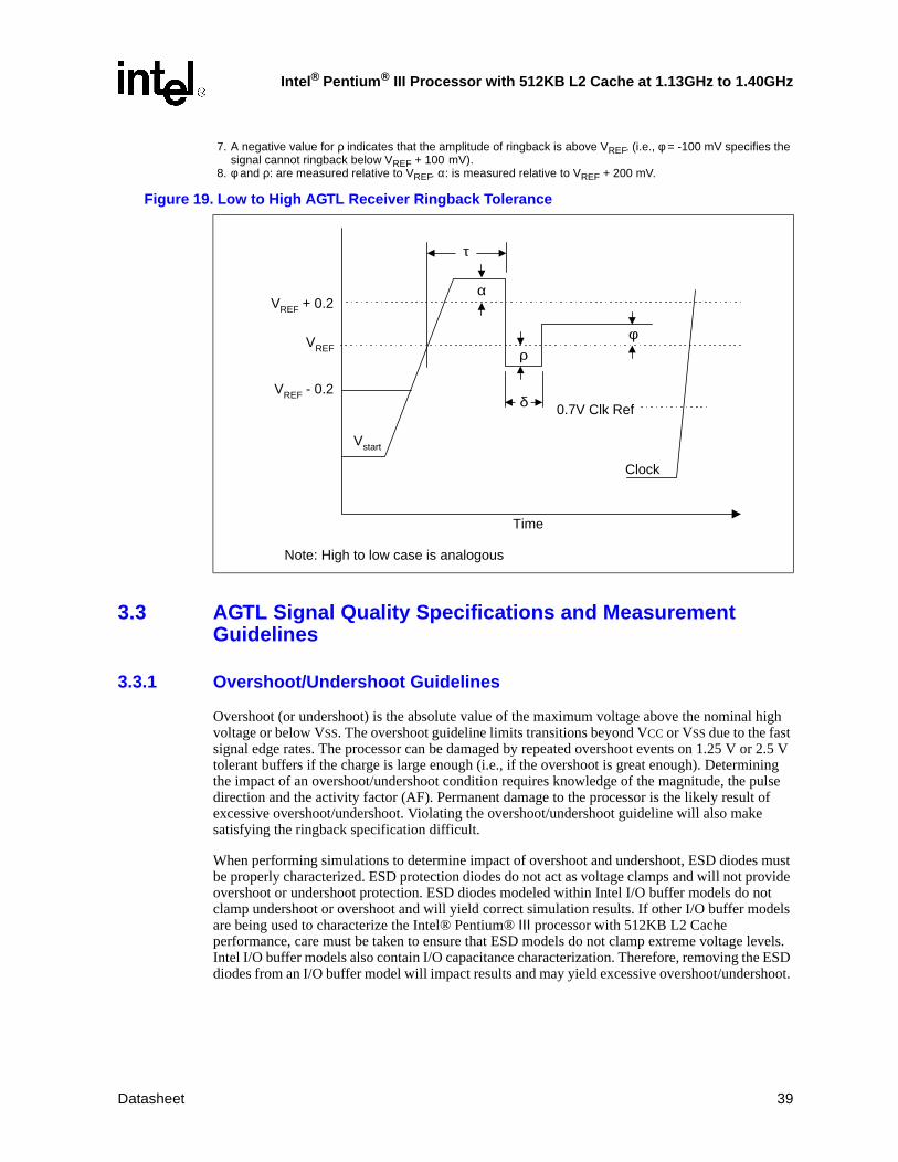
Intel® Pentium® III Processor with 512KB L2 Cache at 1.13GHz to 1.40GHz
7. A negative value for ρ indicates that the amplitude of ringback is above VREF. (i.e., φ = -100 mV specifies the signal cannot ringback below VREF + 100 mV).
8. φ and ρ: are measured relative to VREF. α: is measured relative to VREF + 200 mV.
3.3 AGTL Signal Quality Specifications and Measurement Guidelines
3.3.1 Overshoot/Undershoot Guidelines
Overshoot (or undershoot) is the absolute value of the maximum voltage above the nominal high voltage or below VSS. The overshoot guideline limits transitions beyond VCC or VSS due to the fast signal edge rates. The processor can be damaged by repeated overshoot events on 1.25 V or 2.5 V tolerant buffers if the charge is large enough (i.e., if the overshoot is great enough). Determining the impact of an overshoot/undershoot condition requires knowledge of the magnitude, the pulse direction and the activity factor (AF). Permanent damage to the processor is the likely result of excessive overshoot/undershoot. Violating the overshoot/undershoot guideline will also make satisfying the ringback specification difficult.
When performing simulations to determine impact of overshoot and undershoot, ESD diodes must be properly characterized. ESD protection diodes do not act as voltage clamps and will not provide overshoot or undershoot protection. ESD diodes modeled within Intel I/O buffer models do not clamp undershoot or overshoot and will yield correct simulation results. If other I/O buffer models are being used to characterize the Intel® Pentium® III processor with 512KB L2 Cache performance, care must be taken to ensure that ESD models do not clamp extreme voltage levels. Intel I/O buffer models also contain I/O capacitance characterization. Therefore, removing the ESD diodes from an I/O buffer model will impact results and may yield excessive overshoot/undershoot.
Figure 19. Low to High AGTL Receiver Ringback Tolerance
0.7V Clk Ref
Clock
Time
Vstart
VREF - 0.2
VREF
VREF + 0.2
Note: High to low case is analogous
τ
α
δ
ρφ
Datasheet 39
Intel® Pentium® III Processor with 512KB L2 Cache at 1.13GHz to 1.40GHz
3.3.2 Overshoot/Undershoot Magnitude
Magnitude describes the maximum potential difference between a signal and its voltage reference level, VSS (overshoot) and VTT (undershoot). While overshoot can be measured relative to VSS using one probe (probe to signal and GND lead to VSS), undershoot must be measured relative to VTT. This could be accomplished by simultaneously measuring the VTT plane while measuring the signal undershoot. Today’s oscilloscopes can easily calculate the true undershoot waveform. The true undershoot waveform can also be obtained with the following oscilloscope data file analysis:
Converted Undershoot Waveform = VTT - Signal_measured
Note: The converted undershoot waveform appears as a positive (overshoot) signal.
Note: Overshoot (rising edge) and undershoot (falling edge) conditions are separate and their impact must be determined independently.
After the true waveform conversion, the undershoot/overshoot specifications shown in Table 24 through Table 27 can be applied to the converted undershoot waveform using the same magnitude and pulse duration specifications used with an overshoot waveform.
Overshoot/undershoot magnitude levels must observe the Absolute Maximum Specifications listed in Table 24 through Table 27. These specifications must not be violated at any time regardless of bus activity or system state. Within these specifications are threshold levels that define different allowed pulse durations. Provided that the magnitude of the overshoot/undershoot is within the Absolute Maximum Specifications (1.78V AGTL, 2.08V CMOS), the pulse magnitude, duration and activity factor must all be used to determine if the overshoot/undershoot pulse is within specifications.
3.3.3 Overshoot/Undershoot Pulse Duration
Pulse duration describes the total time an overshoot/undershoot event exceeds the overshoot/undershoot reference voltage (Vos_ref = 1.32V AGTL, 1.80V CMOS). The total time could encompass several oscillations above the reference voltage. Multiple overshoot/undershoot pulses within a single overshoot/undershoot event may need to be measured to determine the total pulse duration.
Note: Oscillations below the reference voltage can not be subtracted from the total overshoot/undershoot pulse duration.
Note: Multiple Overshoot/Undershoot events occurring within the same clock cycle must be considered together as one event. Using the worst case Overshoot/Undershoot Magnitude, sum together the individual Pulse Durations to determine the total Overshoot/Undershoot Pulse Duration for that total event.
3.3.4 Activity Factor
Activity Factor (AF) describes the frequency of overshoot (or undershoot) occurrence relative to a clock. Since the highest frequency of assertion of an AGTL or a CMOS signal is every other clock, an AF = 1 indicates that the specific overshoot (or undershoot) waveform occurs EVERY OTHER clock cycle. Thus, an AF = 0.01 indicates that the specific overshoot (or undershoot) waveform occurs one time in every 200 clock cycles.
The specifications provided in Table 24 through Table 27 show the Maximum Pulse Duration allowed for a given Overshoot/Undershoot Magnitude at a specific Activity Factor. Each Table entry is independent of all others, meaning that the Pulse Duration reflects the existence of overshoot/undershoot events of that magnitude ONLY. A platform with an overshoot/undershoot
40 Datasheet
Intel® Pentium® III Processor with 512KB L2 Cache at 1.13GHz to 1.40GHz
that just meets the pulse duration for a specific magnitude where the AF < 1, means that there can be NO other overshoot/undershoot events, even of lesser magnitude (note that if AF = 1, then the event occurs at all times and no other events can occur).
Note: Activity factor for AGTL signals is referenced to system bus clock frequency.
Note: Activity factor for CMOS signals is referenced to PICCLK frequency.
3.3.5 Reading Overshoot/Undershoot Specification Tables
The overshoot/undershoot specification for the Intel® Pentium® III processor with 512KB L2 cache is not a simple single value. Instead, many factors are needed to determine what the over/undershoot specification is. In addition to the magnitude of the overshoot, the following parameters must also be known: the case temperature the processor will be operating at, the width of the overshoot (as measured above 1.78 V) and the Activity Factor (AF). To determine the allowed overshoot for a particular overshoot event, the following must be done:
1. Determine the signal group that particular signal falls into. If the signal is an AGTL signal operating with a 133 MHz system bus, use Table 25 (133 MHz AGTL signal group). If the signal is a CMOS signal, use Table 27 (33 MHz CMOS signal group).
2. Determine the maximum case temperature (Tcase) for the range of processors that the system will support.
3. Determine the Magnitude of the overshoot (relative to VSS)
4. Determine the Activity Factor (how often this overshoot occurs?)
5. From the appropriate Specification table, read off the Maximum Pulse Duration (in ns) allowed.
6. Compare the specified Maximum Pulse Duration to the signal being measured. If the Pulse Duration measured is less than the Pulse Duration shown in the table, then the signal meets the specifications.
The above procedure is similar for undershoots after the undershoot waveform has been converted to look like an overshoot. Undershoot events must be analyzed separately from Overshoot events as they are mutually exclusive.
Below is an example showing how the maximum pulse duration is determined for a given waveform.
Given the above parameters, and using Table 25 (69oC/AF = 0.1 column) the maximum allowed pulse duration is 7.5 ns. Since the measure pulse duration is 7.5 ns, this particular overshoot event passes the overshoot specifications, although this doesn’t guarantee that the combined overshoot/undershoot events meet the specifications.
Table 24. Example Platform Information
Required Information Maximum Platform Support Notes
FSB Signal Group 133 MHz AGTL
Max Tcase 69 °C
Overshoot Magnitude 1.78 V Measured Value
Activity Factor (AF) 0.1 Measured overshoot occurs on average every 20 clocks
Datasheet 41

Intel® Pentium® III Processor with 512KB L2 Cache at 1.13GHz to 1.40GHz
3.3.6 Determining if a System Meets the Overshoot/Undershoot Specifications
The overshoot/undershoot specifications listed in the following tables specify the allowable overshoot/undershoot for a single overshoot/undershoot event. However most systems will have multiple overshoot and/or undershoot events that each have their own set of parameters (duration, AF and magnitude). While each overshoot on its own may meet the overshoot specification, when you add the total impact of all overshoot events, the system may fail. A guideline to ensure a system passes the overshoot and undershoot specifications is shown below. It is important to meet these guidelines; otherwise, contact your Intel field representative.
1. Ensure no AGTL signal ever exceeds 1.78V and no CMOS signal ever exceeds 2.08V.
OR
2. If only one overshoot/undershoot event magnitude occurs, ensure it meets the over/undershoot specifications in the following tables
OR
3. If multiple overshoots and/or multiple undershoots occur, measure the worst case pulse duration for each magnitude and compare the results against the AF = 1 specifications. If all of these worst case overshoot or undershoot events meet the specifications (measured time < specifications) in the table (where AF=1), then the system passes.
The following notes apply to Table 24 through Table 27.
NOTES:1. Overshoot/Undershoot Magnitude = 1.78V(AGTL), 2.08V(CMOS) is an absolute value and
should never be exceeded2. Overshoot is measured relative to VSS.3. Undershoot is measured relative to VTT4. Overshoot/Undershoot Pulse Duration is measured relative to 1.32V for AGTL and 1.80V for
CMOS. 5. Rinbacks below VTT can not be subtracted from Overshoots/Undershoots6. Lesser Undershoot does not allocate longer or larger Overshoot7. OEM’s are encouraged to follow Intel provided layout guidelines. Consult the layout guidelines
provided in the specific platform design guide.8. All values specified by design characterization
42 Datasheet

Intel® Pentium® III Processor with 512KB L2 Cache at 1.13GHz to 1.40GHz
Notes: 1. Measurements taken at the processor socket pins on the solder-side of the motherboard.2. Overshoot/Undershoot Magnitude = 1.78V is an absolute value and should never be exceeded.3. BCLK Period = 7.5nS.
Table 25. 133 MHz AGTL Signal Group Overshoot/Undershoot Tolerance 1, 2, 3
Overshoot/Undershoot Magnitude (V)
Maximum Pulse Duration at Tcase = 60 °C (ns)
Maximum Pulse Duration at Tcase = 69 °C (ns)
AF = 0.01 AF = 0.1 AF = 1 AF = 0.01 AF = 0.1 AF = 1
1.78 15 1.5 0.153 8.7 0.87 0.087
1.73 15 3.1 0.31 15 2.0 0.20
1.68 15 6.8 0.68 15 4.6 0.46
1.63 15 14 1.42 15 10 1.0
1.58 15 15 2.95 15 15 2.3
1.53 15 15 6.2 15 15 5.0
1.48 15 15 13.2 15 15 15
Figure 20. Maximum Acceptable AGTL Overshoot/Undershoot Waveform
Vos_ref
1.78V Max
1.32V
Vss
Time dependent Overshoot
Time dependent Undershoot
-.46V Min
α β χ
α β χ
.1ns.3ns
1ns
.1ns .3ns 1ns
1.47V1.62V
-.15V-.30V
Datasheet 43

Intel® Pentium® III Processor with 512KB L2 Cache at 1.13GHz to 1.40GHz
3.4 Non-AGTL Signal Quality Specifications and Measurement Guidelines
There are three signal quality parameters defined for non-AGTL signals: overshoot/undershoot, ringback, and settling limit. All three signal quality parameters are shown in Figure 21 for the non-AGTL signal group.
NOTE:1. VHI = 1.80 V for all non-AGTL signals except for BCLK, PICCLK, and PWRGOOD. VHI =2.0 V for PICCLK,
and VHI =1.8 V for PWRGOOD. BCLK and PICCLK signal quality is detailed in Section 3.1.
3.4.1 Overshoot/Undershoot GuidelinesOvershoot (or undershoot) is the absolute value of the maximum voltage above the nominal high voltage or below VSS. The overshoot guideline limits transitions beyond VCC or VSS due to the fast signal edge rates (see Figure 21 for non-AGTL signals). The processor can be damaged by repeated overshoot events on 1.25V or 1.8V tolerant buffers if the charge is large enough (i.e., if the overshoot is great enough). Permanent damage to the processor is the likely result of excessive overshoot/undershoot. Violating the overshoot/undershoot guideline will also make satisfying the ringback specification difficult. The overshoot/undershoot guideline is 0.3V and assumes the absence of diodes on the input. These guidelines should be verified in simulations without the on-chip ESD protection diodes present because the diodes will begin clamping the 1.25V and 2.5V tolerant signals beginning at approximately 0.7V above the appropriate supply and 0.7V below VSS. If signals are not reaching the clamping voltage, this will not be an issue. A system should not rely on the diodes for overshoot/undershoot protection as this will negatively affect the life of the components and make meeting the ringback specification very difficult.
Figure 21. Non-AGTL Overshoot/Undershoot, Settling Limit, and Ringback 1
Undershoot
Overshoot Settling Limit
Settling Limit
Rising-Edge Ringback
Falling-Edge Ringback
V LO
V SS Time
V HI
44 Datasheet
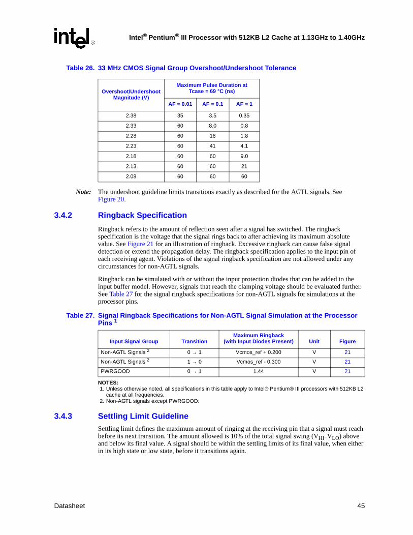
Intel® Pentium® III Processor with 512KB L2 Cache at 1.13GHz to 1.40GHz
Table 26. 33 MHz CMOS Signal Group Overshoot/Undershoot Tolerance
Note: The undershoot guideline limits transitions exactly as described for the AGTL signals. See Figure 20.
3.4.2 Ringback Specification
Ringback refers to the amount of reflection seen after a signal has switched. The ringback specification is the voltage that the signal rings back to after achieving its maximum absolute value. See Figure 21 for an illustration of ringback. Excessive ringback can cause false signal detection or extend the propagation delay. The ringback specification applies to the input pin of each receiving agent. Violations of the signal ringback specification are not allowed under any circumstances for non-AGTL signals.
Ringback can be simulated with or without the input protection diodes that can be added to the input buffer model. However, signals that reach the clamping voltage should be evaluated further. See Table 27 for the signal ringback specifications for non-AGTL signals for simulations at the processor pins.
NOTES:1. Unless otherwise noted, all specifications in this table apply to Intel® Pentium® III processors with 512KB L2
cache at all frequencies.2. Non-AGTL signals except PWRGOOD.
3.4.3 Settling Limit GuidelineSettling limit defines the maximum amount of ringing at the receiving pin that a signal must reach before its next transition. The amount allowed is 10% of the total signal swing (VHI –VLO) above and below its final value. A signal should be within the settling limits of its final value, when either in its high state or low state, before it transitions again.
Overshoot/Undershoot Magnitude (V)
Maximum Pulse Duration at Tcase = 69 °C (ns)
AF = 0.01 AF = 0.1 AF = 1
2.38 35 3.5 0.35
2.33 60 8.0 0.8
2.28 60 18 1.8
2.23 60 41 4.1
2.18 60 60 9.0
2.13 60 60 21
2.08 60 60 60
Table 27. Signal Ringback Specifications for Non-AGTL Signal Simulation at the Processor Pins 1
Input Signal Group TransitionMaximum Ringback
(with Input Diodes Present) Unit Figure
Non-AGTL Signals 2 0 → 1 Vcmos_ref + 0.200 V 21
Non-AGTL Signals 2 1 → 0 Vcmos_ref - 0.300 V 21
PWRGOOD 0 → 1 1.44 V 21
Datasheet 45

Intel® Pentium® III Processor with 512KB L2 Cache at 1.13GHz to 1.40GHz
Signals that are not within their settling limit before transitioning are at risk of unwanted oscillations which could jeopardize signal integrity. Simulations to verify settling limit may be done either with or without the input protection diodes present. Violation of the settling limit guideline is acceptable if simulations of 5 to 10 successive transitions do not show the amplitude of the ringing increasing in the subsequent transitions.
46 Datasheet
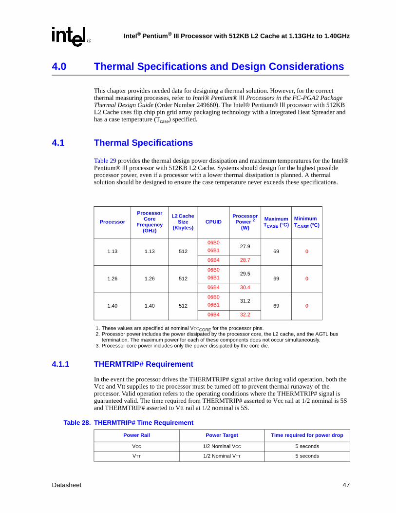
Intel® Pentium® III Processor with 512KB L2 Cache at 1.13GHz to 1.40GHz
4.0 Thermal Specifications and Design Considerations
This chapter provides needed data for designing a thermal solution. However, for the correct thermal measuring processes, refer to Intel® Pentium® III Processors in the FC-PGA2 Package Thermal Design Guide (Order Number 249660). The Intel® Pentium® III processor with 512KB L2 Cache uses flip chip pin grid array packaging technology with a Integrated Heat Spreader and has a case temperature (Tcase) specified.
4.1 Thermal Specifications
Table 29 provides the thermal design power dissipation and maximum temperatures for the Intel® Pentium® III processor with 512KB L2 Cache. Systems should design for the highest possible processor power, even if a processor with a lower thermal dissipation is planned. A thermal solution should be designed to ensure the case temperature never exceeds these specifications.
1. These values are specified at nominal VCCCORE for the processor pins.2. Processor power includes the power dissipated by the processor core, the L2 cache, and the AGTL bus
termination. The maximum power for each of these components does not occur simultaneously.3. Processor core power includes only the power dissipated by the core die.
4.1.1 THERMTRIP# Requirement
In the event the processor drives the THERMTRIP# signal active during valid operation, both the Vcc and Vtt supplies to the processor must be turned off to prevent thermal runaway of the processor. Valid operation refers to the operating conditions where the THERMTRIP# signal is guaranteed valid. The time required from THERMTRIP# asserted to Vcc rail at 1/2 nominal is 5S and THERMTRIP# asserted to Vtt rail at 1/2 nominal is 5S.
Processor
Processor Core
Frequency(GHz)
L2 Cache Size
(Kbytes)CPUID
Processor Power 2
(W)
Maximum TCASE (°C)
Minimum TCASE (°C)
1.13 1.13 512
06B0
06B127.9
69 0
06B4 28.7
1.26 1.26 512
06B0
06B129.5
69 0
06B4 30.4
1.40 1.40 512
06B0
06B131.2
69 0
06B4 32.2
Table 28. THERMTRIP# Time Requirement
Power Rail Power Target Time required for power drop
VCC 1/2 Nominal VCC 5 seconds
VTT 1/2 Nominal VTT 5 seconds
Datasheet 47
Intel® Pentium® III Processor with 512KB L2 Cache at 1.13GHz to 1.40GHz
NOTE: Once Vcc and Vtt supplies are turned off the THERMTRIP# signal will be deactivated. System logic should ensure no “unsafe” power cycling occurs due to this deassertion.
4.1.2 Thermal Diode
The Intel® Pentium® III processor with 512KB L2 Cache incorporates an on-die diode that may be used to monitor the die temperature (junction temperature). A thermal sensor located on the motherboard, or a stand-alone measurement kit, may monitor the die temperature of the processor for thermal management or instrumentation purposes. Table 29 and Table 30 provide the diode parameter and interface specifications.
The Intel® Pentium® III processor with 512KB L2 Cache uses an Integrated Heat Spreader (IHS) and has a case temperature requirement. Please see the Intel® Pentium® III Processors in the FC-PGA2 Package Thermal Design Guide document for details on measuring the case temperature. The thermal diode should be used for system thermal management and not determining spec compliance.
NOTES:1. Intel does not support or recommend operation of the thermal diode under reverse bias.2. Characterized at 75° C with a forward bias current of 5 - 150 µA.3. Characterized at 75° C with a forward bias current of 5 - 300 µA.4. The ideality factor, n, represents the deviation from ideal diode behavior as exemplified by the diode
equation: Ifw=Is(e^ ((Vd*q)/(nkT)) - 1), where Is = saturation current, q = electronic charge, Vd = voltage across the diode, k = Boltzmann Constant, and T = absolute temperature (Kelvin).
5. Not 100% tested. Specified by design characterization.
4.2 Thermal Metrology
The thermal metrology for the Intel® Pentium® III processor in the FC-PGA2 package should be followed to evaluate the thermal performance of proposed cooling solutions. The thermal metrology is contained in the Intel® Pentium® III Processors in the FC-PGA2 Package Thermal Design Guide.
Table 29. Thermal Diode Parameters1
Symbol Parameter Min Typ Max Unit Notes
Ifw Forward Bias Current 5 N/A 150 µA 1
n Diode Ideality Factor 1.001452 1.007152 1.012852 2, 4, 5
Ifw Forward Bias Current 5 N/A 300 µA 1
n Diode Ideality Factor 1.000807 1.009528 1.018249 3, 4, 5
Table 30. Thermal Diode Interface
Pin Name PGA370 Socket pin # Pin Description
THERMDP AL31 diode anode (p_junction)
THERMDN AL29 diode cathode (n_junction)
48 Datasheet
Intel® Pentium® III Processor with 512KB L2 Cache at 1.13GHz to 1.40GHz
5.0 Mechanical Specifications
The Intel® Pentium® III processor with 512KB L2 Cache uses a FC-PGA2 package technology. Mechanical specifications for the processor are given in this section. See Section 1.1.1 for a complete terminology listing.
The processor utilizes a PGA370 socket for installation into the motherboard. Details on the socket are available in the 370-Pin Socket (PGA370) Design Guidelines.
Note: For Figure 22, the following apply:
1. Unless otherwise specified, the following drawings are dimensioned in inches.
2. All dimensions provided with tolerances are guaranteed to be met for all normal production product.
3. Figures and drawings labeled as “Reference Dimensions” are provided for informational purposes only. Reference dimensions are extracted from the mechanical design database and are nominal dimensions with no tolerance information applied. Reference dimensions are NOT checked as part of the processor manufacturing. Unless noted as such, dimensions in parentheses without tolerances are reference dimensions.
4. Drawings are not to scale.
5.1 FC-PGA2 Mechanical Specifications
The following figure with package dimensions is provided to aid in the design of heatsink and clip solutions as well as demonstrate where pin-side capacitors will be located on the processor. Table 31 includes the measurements for these dimensions in both inches and millimeters.
Datasheet 49
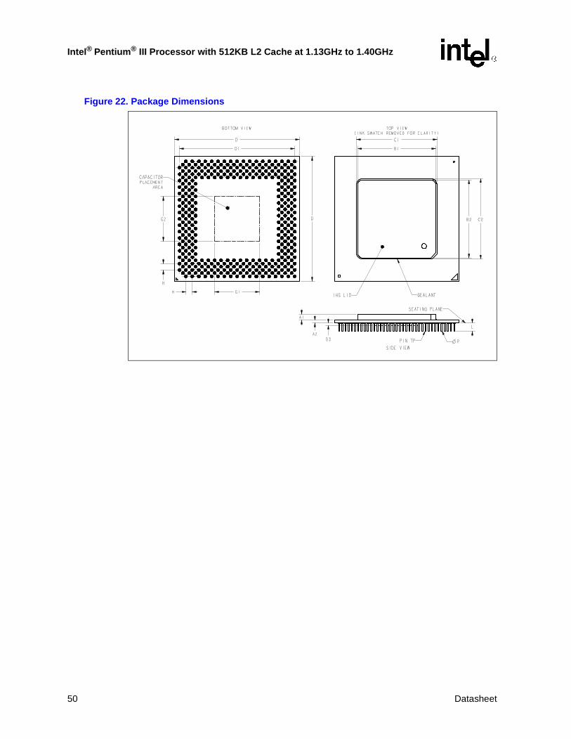
Intel® Pentium® III Processor with 512KB L2 Cache at 1.13GHz to 1.40GHz
Figure 22. Package Dimensions
50 Datasheet
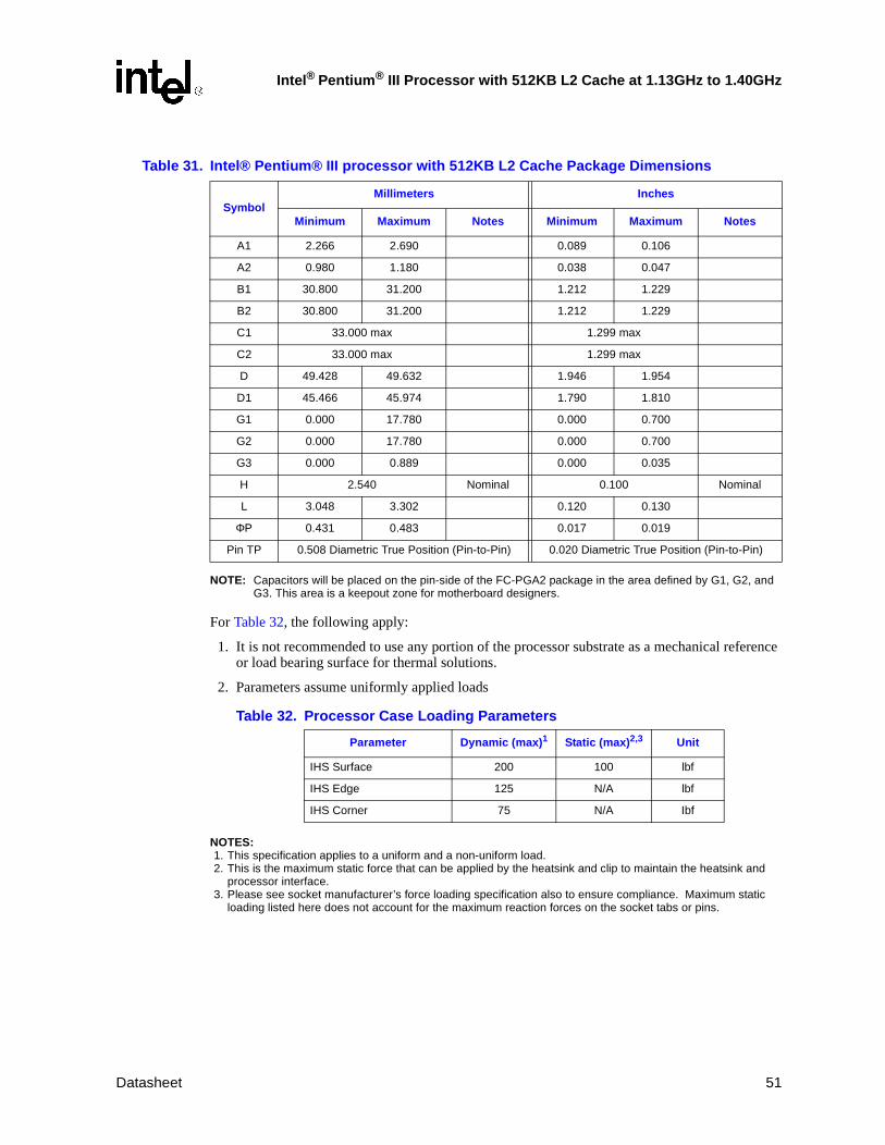
Intel® Pentium® III Processor with 512KB L2 Cache at 1.13GHz to 1.40GHz
NOTE: Capacitors will be placed on the pin-side of the FC-PGA2 package in the area defined by G1, G2, and G3. This area is a keepout zone for motherboard designers.
For Table 32, the following apply:
1. It is not recommended to use any portion of the processor substrate as a mechanical reference or load bearing surface for thermal solutions.
2. Parameters assume uniformly applied loads
NOTES:1. This specification applies to a uniform and a non-uniform load.2. This is the maximum static force that can be applied by the heatsink and clip to maintain the heatsink and
processor interface.3. Please see socket manufacturer’s force loading specification also to ensure compliance. Maximum static
loading listed here does not account for the maximum reaction forces on the socket tabs or pins.
Table 31. Intel® Pentium® III processor with 512KB L2 Cache Package Dimensions
SymbolMillimeters Inches
Minimum Maximum Notes Minimum Maximum Notes
A1 2.266 2.690 0.089 0.106
A2 0.980 1.180 0.038 0.047
B1 30.800 31.200 1.212 1.229
B2 30.800 31.200 1.212 1.229
C1 33.000 max 1.299 max
C2 33.000 max 1.299 max
D 49.428 49.632 1.946 1.954
D1 45.466 45.974 1.790 1.810
G1 0.000 17.780 0.000 0.700
G2 0.000 17.780 0.000 0.700
G3 0.000 0.889 0.000 0.035
H 2.540 Nominal 0.100 Nominal
L 3.048 3.302 0.120 0.130
ΦP 0.431 0.483 0.017 0.019
Pin TP 0.508 Diametric True Position (Pin-to-Pin) 0.020 Diametric True Position (Pin-to-Pin)
Table 32. Processor Case Loading Parameters
Parameter Dynamic (max)1 Static (max)2,3 Unit
IHS Surface 200 100 lbf
IHS Edge 125 N/A lbf
IHS Corner 75 N/A Ibf
Datasheet 51

Intel® Pentium® III Processor with 512KB L2 Cache at 1.13GHz to 1.40GHz
Figure 23. FC-PGA2 IHS Flatness Specification
5.2 Recommended Mechanical Keep-Out Zones
Note: Flatness specifications in millimeters
Figure 24. Volumetric Keep-Out
52 Datasheet
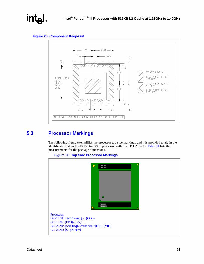
Intel® Pentium® III Processor with 512KB L2 Cache at 1.13GHz to 1.40GHz
5.3 Processor Markings
The following figure exemplifies the processor top-side markings and it is provided to aid in the identification of an Intel® Pentium® III processor with 512KB L2 Cache. Table 31 lists the measurements for the package dimensions.
Figure 25. Component Keep-Out
Figure 26. Top Side Processor Markings
GRP2LN1 GRP2LN2
GRP1LN1 GRP1LN2
Production GRP1LN1: Intel’01 (m)(c)_-_COO GRP1LN2: FPO-S/N GRP2LN1: core freq/cache size/FSB/VID GRP2LN2: S-spec here
Datasheet 53
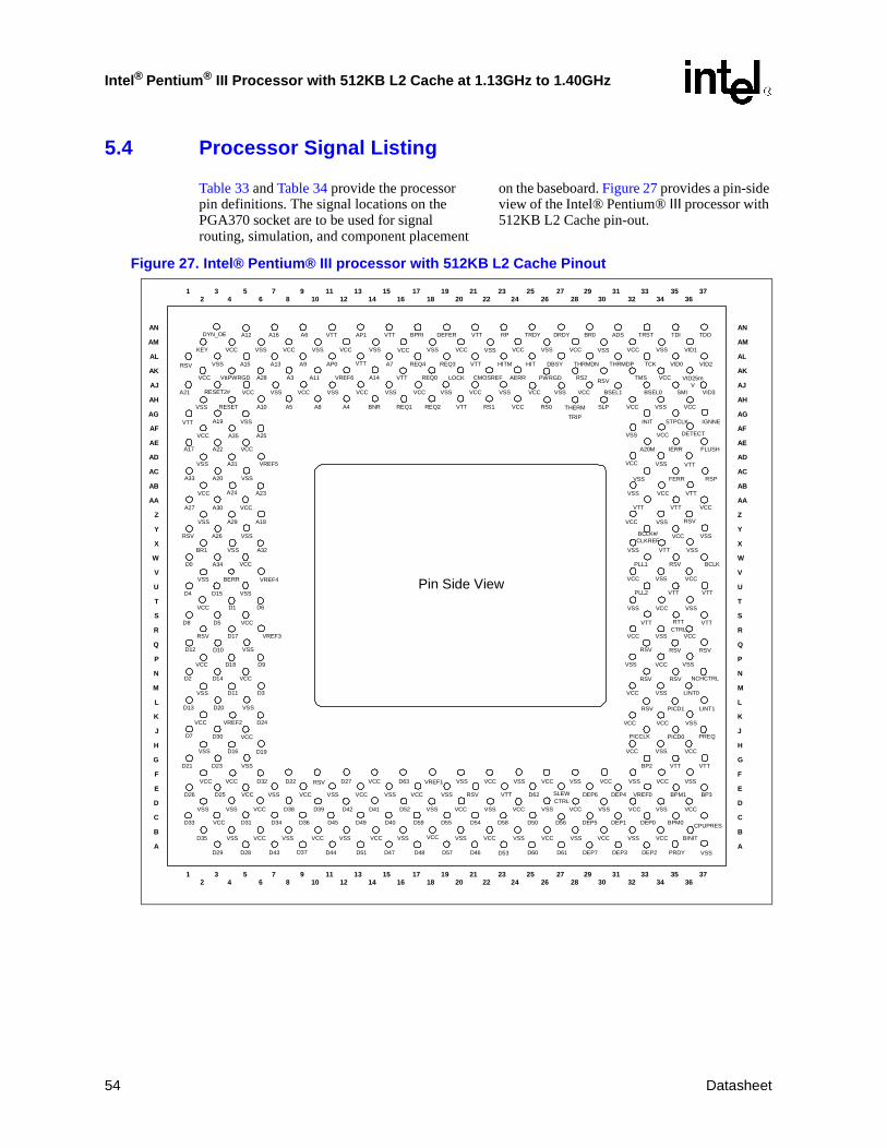
Intel® Pentium® III Processor with 512KB L2 Cache at 1.13GHz to 1.40GHz
5.4 Processor Signal Listing
Table 33 and Table 34 provide the processor pin definitions. The signal locations on the PGA370 socket are to be used for signal routing, simulation, and component placement
on the baseboard. Figure 27 provides a pin-side view of the Intel® Pentium® III processor with 512KB L2 Cache pin-out.
Figure 27. Intel® Pentium® III processor with 512KB L2 Cache Pinout
VSS
VCC
VSSD35
D29
D33
D26
D28
D21 D23
D25
VSS
VCC
VSS
D31
VCC
D43
VCC VSS
D34
D38
VCCVSS
D39
D36
VCC
D37 D44
VCC VCC D32 D22 RSV D27
VSS
D42
D45 D49
VSS
VCC D63 VREF1 VSS VCC VSS VCC VSS VCC VSS VCC VSS
VCC VSS VCC VSS RSV VTT D62 SLEWCTRL
DEP6 DEP4 VREF0 BPM1 BP3
D41 D52 VSS VCC VSS VCC VSS VCC VSS VCC VSS VCC
D40 D59 D55 D54 D58 D50 D56 DEP5 DEP1 DEP0 BPM0 CPUPRES
VCC VSS VCC VSS VCC VSS VCC VSS VCC VSS VCC BINIT
D51 D47 D48 D57 D46 D53 D60 D61 DEP7 DEP3 DEP2 PRDY VSS
BP2 VTT VTT
VCC VSS VCC
PICCLK PICD0 PREQ
VCC VCC VSS
RSV PICD1 LINT1
VCC VSS LINT0
RSV RSV
RSV
VSS VCC VSS
NCHCTRL
RSV RSV
VCC VSS VCC
VTT RTTCTRL
VTT
VSS VCC VSS
PLL2 VTT VTT
VCC VSS VCC
BCLK#/CLKREF
VCC VSS
VCC VSS RSV
VTT VTT VCC
VSS VCC VTT
VSS FERR RSP
VCC VSS VTT
A20M IERR FLUSH
VSS VCC DETECT
INIT
VSS VTT VSS
PLL1 RSV BCLK
STPCLK IGNNE
VSS D16 D19
D7 D30 VCC
VCC VREF2 D24
D13 D20 VSS
VSS D11 D3
D2 D14 VCC
VCC D18 D9
D12 D10 VSS
RSV D17 VREF3
D8 D5 VCC
VCC D1 D6
D4 D15 VSS
VSS BERR VREF4
D0 A34 VCC
BR1 VSS A32
RSV A26 VSS
VSS A29 A18
A27 A30 VCC
VCC A24 A23
A33 A20 VSS
VSS A31 VREF5
A17 A22 VCC
VCC A35 A25
VTT A19 VSS
VSS RESET A10 A5 A8 A4 BNR REQ1 REQ2 VTT RS1 VCC RS0 THERM
TRIP
SLP VCC VSS VCC
A21 RESET2# VCC VSS VCC VSS VCC VSS VCC VSS VCC VSS VCC VSS VCC BSEL1 BSEL0 SMI VID3
VCC VttPWRGD A28 A3 A11 VREF6 A14 VTT REQ0 LOCK CMOSREF AERR PWRGD RS2 RSV TMS VCC VID25mV
RSV VSS A15 A13 A9 AP0 VTT A7 REQ4 REQ3 VTT HITM HIT DBSY THRMDN THRMDP TCK VID0 VID2
KEY VCC VSS VCC VSS VCC VSS VCC VSS VCC VSS VCC VSS VCC VSS VCC VSS VID1
DYN_OE A12 A16 A6 VTT AP1 VTT BPRI DEFER VTT RP TRDY DRDY BR0 ADS TRST TDI TDO
Pin Side View
AN
AM
AL
AK
AJ
AH
AG
AF
AE
AD
AC
AB
AA
Z
Y
X
W
V
U
T
S
R
Q
P
N
M
L
K
J
H
G
F
E
D
C
B
A
AN
AM
AL
AK
AJ
AH
AG
AF
AE
AD
AC
AB
AA
Z
Y
X
W
V
U
T
S
R
Q
P
N
M
L
K
J
H
G
F
E
D
C
B
A
12
34
56
78
910
1112
1314
1516
1718
1920
2122
2324
2526
2728
2930
3132
3334
3536
37
12
34
56
78
910
1112
1314
1516
1718
1920
2122
2324
2526
2728
2930
3132
3334
3536
37
54 Datasheet
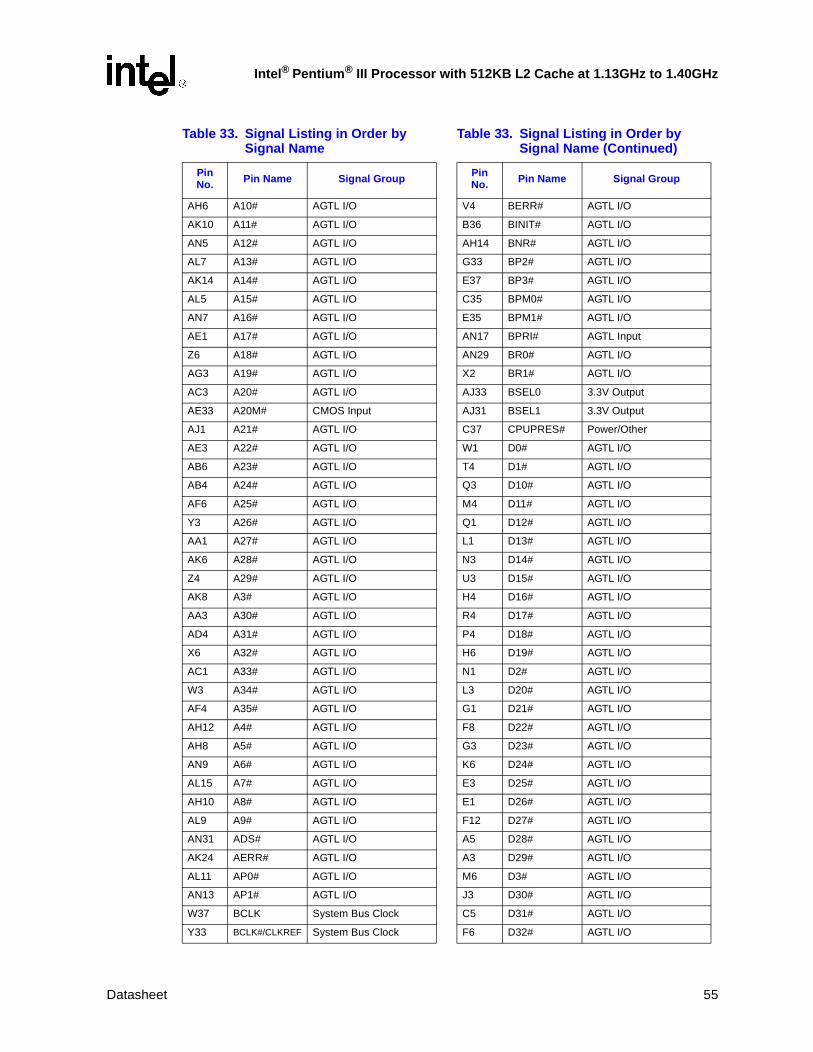
Intel® Pentium® III Processor with 512KB L2 Cache at 1.13GHz to 1.40GHz
Table 33. Signal Listing in Order by Signal Name
Pin No. Pin Name Signal Group
AH6 A10# AGTL I/O
AK10 A11# AGTL I/O
AN5 A12# AGTL I/O
AL7 A13# AGTL I/O
AK14 A14# AGTL I/O
AL5 A15# AGTL I/O
AN7 A16# AGTL I/O
AE1 A17# AGTL I/O
Z6 A18# AGTL I/O
AG3 A19# AGTL I/O
AC3 A20# AGTL I/O
AE33 A20M# CMOS Input
AJ1 A21# AGTL I/O
AE3 A22# AGTL I/O
AB6 A23# AGTL I/O
AB4 A24# AGTL I/O
AF6 A25# AGTL I/O
Y3 A26# AGTL I/O
AA1 A27# AGTL I/O
AK6 A28# AGTL I/O
Z4 A29# AGTL I/O
AK8 A3# AGTL I/O
AA3 A30# AGTL I/O
AD4 A31# AGTL I/O
X6 A32# AGTL I/O
AC1 A33# AGTL I/O
W3 A34# AGTL I/O
AF4 A35# AGTL I/O
AH12 A4# AGTL I/O
AH8 A5# AGTL I/O
AN9 A6# AGTL I/O
AL15 A7# AGTL I/O
AH10 A8# AGTL I/O
AL9 A9# AGTL I/O
AN31 ADS# AGTL I/O
AK24 AERR# AGTL I/O
AL11 AP0# AGTL I/O
AN13 AP1# AGTL I/O
W37 BCLK System Bus Clock
Y33 BCLK#/CLKREF System Bus Clock
V4 BERR# AGTL I/O
B36 BINIT# AGTL I/O
AH14 BNR# AGTL I/O
G33 BP2# AGTL I/O
E37 BP3# AGTL I/O
C35 BPM0# AGTL I/O
E35 BPM1# AGTL I/O
AN17 BPRI# AGTL Input
AN29 BR0# AGTL I/O
X2 BR1# AGTL I/O
AJ33 BSEL0 3.3V Output
AJ31 BSEL1 3.3V Output
C37 CPUPRES# Power/Other
W1 D0# AGTL I/O
T4 D1# AGTL I/O
Q3 D10# AGTL I/O
M4 D11# AGTL I/O
Q1 D12# AGTL I/O
L1 D13# AGTL I/O
N3 D14# AGTL I/O
U3 D15# AGTL I/O
H4 D16# AGTL I/O
R4 D17# AGTL I/O
P4 D18# AGTL I/O
H6 D19# AGTL I/O
N1 D2# AGTL I/O
L3 D20# AGTL I/O
G1 D21# AGTL I/O
F8 D22# AGTL I/O
G3 D23# AGTL I/O
K6 D24# AGTL I/O
E3 D25# AGTL I/O
E1 D26# AGTL I/O
F12 D27# AGTL I/O
A5 D28# AGTL I/O
A3 D29# AGTL I/O
M6 D3# AGTL I/O
J3 D30# AGTL I/O
C5 D31# AGTL I/O
F6 D32# AGTL I/O
Table 33. Signal Listing in Order by Signal Name (Continued)
Pin No. Pin Name Signal Group
Datasheet 55
Intel® Pentium® III Processor with 512KB L2 Cache at 1.13GHz to 1.40GHz
C1 D33# AGTL I/O
C7 D34# AGTL I/O
B2 D35# AGTL I/O
C9 D36# AGTL I/O
A9 D37# AGTL I/O
D8 D38# AGTL I/O
D10 D39# AGTL I/O
U1 D4# AGTL I/O
C15 D40# AGTL I/O
D14 D41# AGTL I/O
D12 D42# AGTL I/O
A7 D43# AGTL I/O
A11 D44# AGTL I/O
C11 D45# AGTL I/O
A21 D46# AGTL I/O
A15 D47# AGTL I/O
A17 D48# AGTL I/O
C13 D49# AGTL I/O
S3 D5# AGTL I/O
C25 D50# AGTL I/O
A13 D51# AGTL I/O
D16 D52# AGTL I/O
A23 D53# AGTL I/O
C21 D54# AGTL I/O
C19 D55# AGTL I/O
C27 D56# AGTL I/O
A19 D57# AGTL I/O
C23 D58# AGTL I/O
C17 D59# AGTL I/O
T6 D6# AGTL I/O
A25 D60# AGTL I/O
A27 D61# AGTL I/O
E25 D62# AGTL I/O
F16 D63# AGTL I/O
J1 D7# AGTL I/O
S1 D8# AGTL I/O
P6 D9# AGTL I/O
AL27 DBSY# AGTL I/O
AN19 DEFER# AGTL Input
C33 DEP0# AGTL I/O
Table 33. Signal Listing in Order by Signal Name (Continued)
Pin No. Pin Name Signal Group
C31 DEP1# AGTL I/O
A33 DEP2# AGTL I/O
A31 DEP3# AGTL I/O
E31 DEP4# AGTL I/O
C29 DEP5# AGTL I/O
E29 DEP6# AGTL I/O
A29 DEP7# AGTL I/O
AF36 DETECT Power/Other
AN27 DRDY# AGTL I/O
AN3 DYN_OE Power/Other
AC35 FERR# CMOS Output
AE37 FLUSH# CMOS Input
AL25 HIT# AGTL I/O
AL23 HITM# AGTL I/O
AE35 IERR# CMOS Output
AG37 IGNNE# CMOS Input
AG33 INIT# CMOS Input
AM2 KEY Power/Other
M36 LINT0/INTR CMOS Input
L37 LINT1/NMI CMOS Input
AK20 LOCK# AGTL I/O
N37 NCHCTRL Power/Other
J33 PICCLK APIC Clock Input
J35 PICD0 APIC I/O
L35 PICD1 APIC I/O
W33 PLL1 Power/Other
U33 PLL2 Power/Other
A35 PRDY# AGTL Output
J37 PREQ# CMOS Input
AK26 PWRGOOD CMOS Input
AK18 REQ0# AGTL I/O
AH16 REQ1# AGTL I/O
AH18 REQ2# AGTL I/O
AL19 REQ3# AGTL I/O
AL17 REQ4# AGTL I/O
AK30 Reserved Reserved for future use
AL1 Reserved Reserved for future use
F10 Reserved Reserved for future use
E21 Reserved Reserved for future use
L33 Reserved Reserved for future use
Table 33. Signal Listing in Order by Signal Name (Continued)
Pin No. Pin Name Signal Group
56 Datasheet

Intel® Pentium® III Processor with 512KB L2 Cache at 1.13GHz to 1.40GHz
Table 33. Signal Listing in Order by Signal Name
Pin No. Pin Name Signal Group
AH6 A10# AGTL I/O
AK10 A11# AGTL I/O
AN5 A12# AGTL I/O
AL7 A13# AGTL I/O
AK14 A14# AGTL I/O
AL5 A15# AGTL I/O
AN7 A16# AGTL I/O
AE1 A17# AGTL I/O
Z6 A18# AGTL I/O
AG3 A19# AGTL I/O
AC3 A20# AGTL I/O
AE33 A20M# CMOS Input
AJ1 A21# AGTL I/O
AE3 A22# AGTL I/O
AB6 A23# AGTL I/O
AB4 A24# AGTL I/O
AF6 A25# AGTL I/O
Y3 A26# AGTL I/O
AA1 A27# AGTL I/O
AK6 A28# AGTL I/O
Z4 A29# AGTL I/O
AK8 A3# AGTL I/O
AA3 A30# AGTL I/O
AD4 A31# AGTL I/O
X6 A32# AGTL I/O
AC1 A33# AGTL I/O
W3 A34# AGTL I/O
AF4 A35# AGTL I/O
AH12 A4# AGTL I/O
AH8 A5# AGTL I/O
AN9 A6# AGTL I/O
AL15 A7# AGTL I/O
AH10 A8# AGTL I/O
AL9 A9# AGTL I/O
AN31 ADS# AGTL I/O
AK24 AERR# AGTL I/O
AL11 AP0# AGTL I/O
AN13 AP1# AGTL I/O
W37 BCLK System Bus Clock
Y33 BCLK#/CLKREF System Bus Clock
V4 BERR# AGTL I/O
B36 BINIT# AGTL I/O
AH14 BNR# AGTL I/O
G33 BP2# AGTL I/O
E37 BP3# AGTL I/O
C35 BPM0# AGTL I/O
E35 BPM1# AGTL I/O
AN17 BPRI# AGTL Input
AN29 BR0# AGTL I/O
X2 BR1# AGTL I/O
AJ33 BSEL0 3.3V Output
AJ31 BSEL1 3.3V Output
C37 CPUPRES# Power/Other
W1 D0# AGTL I/O
T4 D1# AGTL I/O
Q3 D10# AGTL I/O
M4 D11# AGTL I/O
Q1 D12# AGTL I/O
L1 D13# AGTL I/O
N3 D14# AGTL I/O
U3 D15# AGTL I/O
H4 D16# AGTL I/O
R4 D17# AGTL I/O
P4 D18# AGTL I/O
H6 D19# AGTL I/O
N1 D2# AGTL I/O
L3 D20# AGTL I/O
G1 D21# AGTL I/O
F8 D22# AGTL I/O
G3 D23# AGTL I/O
K6 D24# AGTL I/O
E3 D25# AGTL I/O
E1 D26# AGTL I/O
F12 D27# AGTL I/O
A5 D28# AGTL I/O
A3 D29# AGTL I/O
M6 D3# AGTL I/O
J3 D30# AGTL I/O
C5 D31# AGTL I/O
F6 D32# AGTL I/O
Table 33. Signal Listing in Order by Signal Name (Continued)
Pin No. Pin Name Signal Group
Datasheet 57

Intel® Pentium® III Processor with 512KB L2 Cache at 1.13GHz to 1.40GHz
C1 D33# AGTL I/O
C7 D34# AGTL I/O
B2 D35# AGTL I/O
C9 D36# AGTL I/O
A9 D37# AGTL I/O
D8 D38# AGTL I/O
D10 D39# AGTL I/O
U1 D4# AGTL I/O
C15 D40# AGTL I/O
D14 D41# AGTL I/O
D12 D42# AGTL I/O
A7 D43# AGTL I/O
A11 D44# AGTL I/O
C11 D45# AGTL I/O
A21 D46# AGTL I/O
A15 D47# AGTL I/O
A17 D48# AGTL I/O
C13 D49# AGTL I/O
S3 D5# AGTL I/O
C25 D50# AGTL I/O
A13 D51# AGTL I/O
D16 D52# AGTL I/O
A23 D53# AGTL I/O
C21 D54# AGTL I/O
C19 D55# AGTL I/O
C27 D56# AGTL I/O
A19 D57# AGTL I/O
C23 D58# AGTL I/O
C17 D59# AGTL I/O
T6 D6# AGTL I/O
A25 D60# AGTL I/O
A27 D61# AGTL I/O
E25 D62# AGTL I/O
F16 D63# AGTL I/O
J1 D7# AGTL I/O
S1 D8# AGTL I/O
P6 D9# AGTL I/O
AL27 DBSY# AGTL I/O
AN19 DEFER# AGTL Input
C33 DEP0# AGTL I/O
Table 33. Signal Listing in Order by Signal Name (Continued)
Pin No. Pin Name Signal Group
C31 DEP1# AGTL I/O
A33 DEP2# AGTL I/O
A31 DEP3# AGTL I/O
E31 DEP4# AGTL I/O
C29 DEP5# AGTL I/O
E29 DEP6# AGTL I/O
A29 DEP7# AGTL I/O
AF36 DETECT Power/Other
AN27 DRDY# AGTL I/O
AN3 DYN_OE Power/Other
AC35 FERR# CMOS Output
AE37 FLUSH# CMOS Input
AL25 HIT# AGTL I/O
AL23 HITM# AGTL I/O
AE35 IERR# CMOS Output
AG37 IGNNE# CMOS Input
AG33 INIT# CMOS Input
AM2 KEY Power/Other
M36 LINT0/INTR CMOS Input
L37 LINT1/NMI CMOS Input
AK20 LOCK# AGTL I/O
N37 NCHCTRL Power/Other
J33 PICCLK APIC Clock Input
J35 PICD0 APIC I/O
L35 PICD1 APIC I/O
W33 PLL1 Power/Other
U33 PLL2 Power/Other
A35 PRDY# AGTL Output
J37 PREQ# CMOS Input
AK26 PWRGOOD CMOS Input
AK18 REQ0# AGTL I/O
AH16 REQ1# AGTL I/O
AH18 REQ2# AGTL I/O
AL19 REQ3# AGTL I/O
AL17 REQ4# AGTL I/O
AK30 Reserved Reserved for future use
AL1 Reserved Reserved for future use
F10 Reserved Reserved for future use
E21 Reserved Reserved for future use
L33 Reserved Reserved for future use
Table 33. Signal Listing in Order by Signal Name (Continued)
Pin No. Pin Name Signal Group
58 Datasheet
Intel® Pentium® III Processor with 512KB L2 Cache at 1.13GHz to 1.40GHz
N33 Reserved Reserved for future use
N35 Reserved Reserved for future use
Q33 Reserved Reserved for future use
Q35 Reserved Reserved for future use
Q37 Reserved Reserved for future use
R2 Reserved Reserved for future use
W35 Reserved Reserved for future use
Y1 Reserved Reserved for future use
Z36 Reserved Reserved for future use
AH4 RESET# AGTL Input
AJ3 RESET2# AGTL Input
AN23 RP# AGTL I/O
AH26 RS0# AGTL + Input
AH22 RS1# AGTL Input
AK28 RS2# AGTL Input
AC37 RSP# AGTL Input
S35 RTTCTRL Power/Other
E27 SLEWCTRL Power/Other
AH30 SLP# CMOS Input
AJ35 SMI# CMOS Input
AG35 STPCLK# CMOS Input
AL33 TCK TAP Input
AN35 TDI TAP Input
AN37 TDO TAP Output
AL29 THERMDN Power/Other
AL31 THERMDP Power/Other
AH28 THERMTRIP# CMOS Output
AK32 TMS TAP Input
AN25 TRDY# AGTL Input
AN33 TRST# TAP Input
AA37 VCCCORE Power/Other
AA5 VCCCORE Power/Other
AB2 VCCCORE Power/Other
AB34 VCCCORE Power/Other
AD32 VCCCORE Power/Other
AE5 VCCCORE Power/Other
AF2 VCCCORE Power/Other
AF34 VCCCORE Power/Other
AH24 VCCCORE Power/Other
AH32 VCCCORE Power/Other
Table 33. Signal Listing in Order by Signal Name (Continued)
Pin No. Pin Name Signal Group
AH36 VCCCORE Power/Other
AJ13 VCCCORE Power/Other
AJ17 VCCCORE Power/Other
AJ21 VCCCORE Power/Other
AJ25 VCCCORE Power/Other
AJ29 VCCCORE Power/Other
AJ5 VCCCORE Power/Other
AJ9 VCCCORE Power/Other
AK2 VCCCORE Power/Other
AK34 VCCCORE Power/Other
AM12 VCCCORE Power/Other
AM16 VCCCORE Power/Other
AM20 VCCCORE Power/Other
AM24 VCCCORE Power/Other
AM28 VCCCORE Power/Other
AM32 VCCCORE Power/Other
AM4 VCCCORE Power/Other
AM8 VCCCORE Power/Other
B10 VCCCORE Power/Other
B14 VCCCORE Power/Other
B18 VCCCORE Power/Other
B22 VCCCORE Power/Other
B26 VCCCORE Power/Other
B30 VCCCORE Power/Other
B34 VCCCORE Power/Other
B6 VCCCORE Power/Other
C3 VCCCORE Power/Other
D20 VCCCORE Power/Other
D24 VCCCORE Power/Other
D28 VCCCORE Power/Other
D32 VCCCORE Power/Other
D36 VCCCORE Power/Other
D6 VCCCORE Power/Other
E13 VCCCORE Power/Other
E17 VCCCORE Power/Other
E5 VCCCORE Power/Other
E9 VCCCORE Power/Other
F14 VCCCORE Power/Other
F2 VCCCORE Power/Other
F22 VCCCORE Power/Other
Table 33. Signal Listing in Order by Signal Name (Continued)
Pin No. Pin Name Signal Group
Datasheet 59
Intel® Pentium® III Processor with 512KB L2 Cache at 1.13GHz to 1.40GHz
F26 VCCCORE Power/Other
F30 VCCCORE Power/Other
F34 VCCCORE Power/Other
F4 VCCCORE Power/Other
H32 VCCCORE Power/Other
H36 VCCCORE Power/Other
J5 VCCCORE Power/Other
K2 VCCCORE Power/Other
K32 VCCCORE Power/Other
K34 VCCCORE Power/Other
M32 VCCCORE Power/Other
N5 VCCCORE Power/Other
P2 VCCCORE Power/Other
P34 VCCCORE Power/Other
R32 VCCCORE Power/Other
R36 VCCCORE Power/Other
S5 VCCCORE Power/Other
T2 VCCCORE Power/Other
T34 VCCCORE Power/Other
V32 VCCCORE Power/Other
V36 VCCCORE Power/Other
W5 VCCCORE Power/Other
Y35 VCCCORE Power/Other
Z32 VCCCORE Power/Other
AK22 VCMOS_REF Power/Other
AK36 VID 25mV 3.3V Output
AL35 VID0 3.3V Output
AM36 VID1 3.3V Output
AL37 VID2 3.3V Output
AJ37 VID3 3.3V Output
E33 VREF0 Power/Other
F18 VREF1 Power/Other
K4 VREF2 Power/Other
R6 VREF3 Power/Other
V6 VREF4 Power/Other
AD6 VREF5 Power/Other
AK12 VREF6 Power/Other
A37 Vss Power/Other
AB32 Vss Power/Other
AC33 Vss Power/Other
Table 33. Signal Listing in Order by Signal Name (Continued)
Pin No. Pin Name Signal Group
AC5 Vss Power/Other
AD2 Vss Power/Other
AD34 Vss Power/Other
AF32 Vss Power/Other
AG5 Vss Power/Other
AH2 Vss Power/Other
AH34 Vss Power/Other
AJ11 Vss Power/Other
AJ15 Vss Power/Other
AJ19 Vss Power/Other
AJ23 Vss Power/Other
AJ27 Vss Power/Other
AJ7 Vss Power/Other
AL3 Vss Power/Other
AM10 Vss Power/Other
AM14 Vss Power/Other
AM18 Vss Power/Other
AM22 Vss Power/Other
AM26 Vss Power/Other
AM30 Vss Power/Other
AM34 Vss Power/Other
AM6 Vss Power/Other
B12 Vss Power/Other
B16 Vss Power/Other
B20 Vss Power/Other
B24 Vss Power/Other
B28 Vss Power/Other
B32 Vss Power/Other
B4 Vss Power/Other
B8 Vss Power/Other
D18 Vss Power/Other
D2 Vss Power/Other
D22 Vss Power/Other
D26 Vss Power/Other
D30 Vss Power/Other
D34 Vss Power/Other
D4 Vss Power/Other
E11 Vss Power/Other
E15 Vss Power/Other
E19 Vss Power/Other
Table 33. Signal Listing in Order by Signal Name (Continued)
Pin No. Pin Name Signal Group
60 Datasheet

Intel® Pentium® III Processor with 512KB L2 Cache at 1.13GHz to 1.40GHz
E7 Vss Power/Other
F20 Vss Power/Other
F24 Vss Power/Other
F28 Vss Power/Other
F32 Vss Power/Other
F36 Vss Power/Other
G5 Vss Power/Other
H2 Vss Power/Other
H34 Vss Power/Other
K36 Vss Power/Other
L5 Vss Power/Other
M2 Vss Power/Other
M34 Vss Power/Other
P32 Vss Power/Other
P36 Vss Power/Other
Q5 Vss Power/Other
R34 Vss Power/Other
T32 Vss Power/Other
T36 Vss Power/Other
U5 Vss Power/Other
V2 Vss Power/Other
V34 Vss Power/Other
X32 Vss Power/Other
X36 Vss Power/Other
X4 Vss Power/Other
Y37 Vss Power/Other
Y5 Vss Power/Other
Z2 Vss Power/Other
Z34 Vss Power/Other
AB36 VTT Power/Other
AD36 VTT Power/Other
AG1 VTT Power/Other
AH20 VTT Power/Other
AK16 VTT Power/Other
AL13 VTT Power/Other
AL21 VTT Power/Other
AN11 VTT Power/Other
AN15 VTT Power/Other
E23 VTT Power/Other
G35 VTT Power/Other
Table 33. Signal Listing in Order by Signal Name (Continued)
Pin No. Pin Name Signal Group
G37 VTT Power/Other
S33 VTT Power/Other
X34 VTT Power/Other
AA33 VTT Power/Other
AA35 VTT Power/Other
AN21 VTT Power/Other
S37 VTT Power/Other
U35 VTT Power/Other
U37 VTT Power/Other
AK4 VTT_PWRGD Power/Other
Table 33. Signal Listing in Order by Signal Name (Continued)
Pin No. Pin Name Signal Group
Datasheet 61
Intel® Pentium® III Processor with 512KB L2 Cache at 1.13GHz to 1.40GHz
Table 34. Signal Listing in Order by Pin Number
Pin No. Pin Name Signal Group
A3 D29# AGTL I/O
A5 D28# AGTL I/O
A7 D43# AGTL I/O
A9 D37# AGTL I/O
A11 D44# AGTL I/O
A13 D51# AGTL I/O
A15 D47# AGTL I/O
A17 D48# AGTL I/O
A19 D57# AGTL I/O
A21 D46# AGTL I/O
A23 D53# AGTL I/O
A25 D60# AGTL I/O
A27 D61# AGTL I/O
A29 DEP7# AGTL I/O
A31 DEP3# AGTL I/O
A33 DEP2# AGTL I/O
A35 PRDY# AGTL Output
A37 Vss Power/Other
AA1 A27# AGTL I/O
AA3 A30# AGTL I/O
AA5 VCCCORE Power/Other
AA33 VTT Power/Other
AA35 VTT Power/Other
AA37 VCCCORE Power/Other
AB2 VCCCORE Power/Other
AB4 A24# AGTL I/O
AB6 A23# AGTL I/O
AB32 Vss Power/Other
AB34 VCCCORE Power/Other
AB36 VTT Power/Other
AC1 A33# AGTL I/O
AC3 A20# AGTL I/O
AC5 Vss Power/Other
AC33 Vss Power/Other
AC35 FERR# CMOS Output
AC37 RSP# AGTL Input
AD2 Vss Power/Other
AD4 A31# AGTL I/O
AD6 VREF5 Power/Other
AD32 VCCCORE Power/Other
AD34 Vss Power/Other
AD36 VTT Power/Other
AE1 A17# AGTL I/O
AE3 A22# AGTL I/O
AE5 VCCCORE Power/Other
AE33 A20M# CMOS Input
AE35 IERR# CMOS Output
AE37 FLUSH# CMOS Input
AF2 VCCCORE Power/Other
AF4 A35# AGTL I/O
AF6 A25# AGTL I/O
AF32 Vss Power/Other
AF34 VCCCORE Power/Other
AF36 DETECT Power/Other
AG1 VTT Power/Other
AG3 A19# AGTL I/O
AG5 Vss Power/Other
AG33 INIT# CMOS Input
AG35 STPCLK# CMOS Input
AG37 IGNNE# CMOS Input
AH2 Vss Power/Other
AH4 RESET# AGTL Input
AH6 A10# AGTL I/O
AH8 A5# AGTL I/O
AH10 A8# AGTL I/O
AH12 A4# AGTL I/O
AH14 BNR# AGTL I/O
AH16 REQ1# AGTL I/O
AH18 REQ2# AGTL I/O
AH20 VTT Power/Other
AH22 RS1# AGTL Input
AH24 VCCCORE Power/Other
AH26 RS0# AGTL + Input
AH28 THERMTRIP# CMOS Output
AH30 SLP# CMOS Input
AH32 VCCCORE Power/Other
AH34 Vss Power/Other
AH36 VCCCORE Power/Other
AJ1 A21# AGTL I/O
AJ3 RESET2# AGTL Input
Table 34. Signal Listing in Order by Pin Number (Continued)
Pin No. Pin Name Signal Group
62 Datasheet
Intel® Pentium® III Processor with 512KB L2 Cache at 1.13GHz to 1.40GHz
AJ5 VCCCORE Power/Other
AJ7 Vss Power/Other
AJ9 VCCCORE Power/Other
AJ11 Vss Power/Other
AJ13 VCCCORE Power/Other
AJ15 Vss Power/Other
AJ17 VCCCORE Power/Other
AJ19 Vss Power/Other
AJ21 VCCCORE Power/Other
AJ23 Vss Power/Other
AJ25 VCCCORE Power/Other
AJ27 Vss Power/Other
AJ29 VCCCORE Power/Other
AJ31 BSEL1 3.3V Output
AJ33 BSEL0 3.3V Output
AJ35 SMI# CMOS Input
AJ37 VID3 3.3V Output
AK2 VCCCORE Power/Other
AK4 VTT_PWRGD Power/Other
AK6 A28# AGTL I/O
AK8 A3# AGTL I/O
AK10 A11# AGTL I/O
AK12 VREF6 Power/Other
AK14 A14# AGTL I/O
AK16 VTT Power/Other
AK18 REQ0# AGTL I/O
AK20 LOCK# AGTL I/O
AK22 VCMOS_REF Power/Other
AK24 AERR# AGTL I/O
AK26 PWRGOOD CMOS Input
AK28 RS2# AGTL Input
AK30 Reserved Reserved for future use
AK32 TMS TAP Input
AK34 VCCCORE Power/Other
AK36 VID 25mV 3.3V Output
AL1 Reserved Reserved for future use
AL3 Vss Power/Other
AL5 A15# AGTL I/O
AL7 A13# AGTL I/O
AL9 A9# AGTL I/O
Table 34. Signal Listing in Order by Pin Number (Continued)
Pin No. Pin Name Signal Group
AL11 AP0# AGTL I/O
AL13 VTT Power/Other
AL15 A7# AGTL I/O
AL17 REQ4# AGTL I/O
AL19 REQ3# AGTL I/O
AL21 VTT Power/Other
AL23 HITM# AGTL I/O
AL25 HIT# AGTL I/O
AL27 DBSY# AGTL I/O
AL29 THERMDN Power/Other
AL31 THERMDP Power/Other
AL33 TCK TAP Input
AL35 VID0 3.3V Output
AL37 VID2 3.3V Output
AM2 KEY Power/Other
AM4 VCCCORE Power/Other
AM6 Vss Power/Other
AM8 VCCCORE Power/Other
AM10 Vss Power/Other
AM12 VCCCORE Power/Other
AM14 Vss Power/Other
AM16 VCCCORE Power/Other
AM18 Vss Power/Other
AM20 VCCCORE Power/Other
AM22 Vss Power/Other
AM24 VCCCORE Power/Other
AM26 Vss Power/Other
AM28 VCCCORE Power/Other
AM30 Vss Power/Other
AM32 VCCCORE Power/Other
AM34 Vss Power/Other
AM36 VID1 3.3V Output
AN3 DYN_OE Power/Other
AN5 A12# AGTL I/O
AN7 A16# AGTL I/O
AN9 A6# AGTL I/O
AN11 VTT Power/Other
AN13 AP1# AGTL I/O
AN15 VTT Power/Other
AN17 BPRI# AGTL Input
Table 34. Signal Listing in Order by Pin Number (Continued)
Pin No. Pin Name Signal Group
Datasheet 63
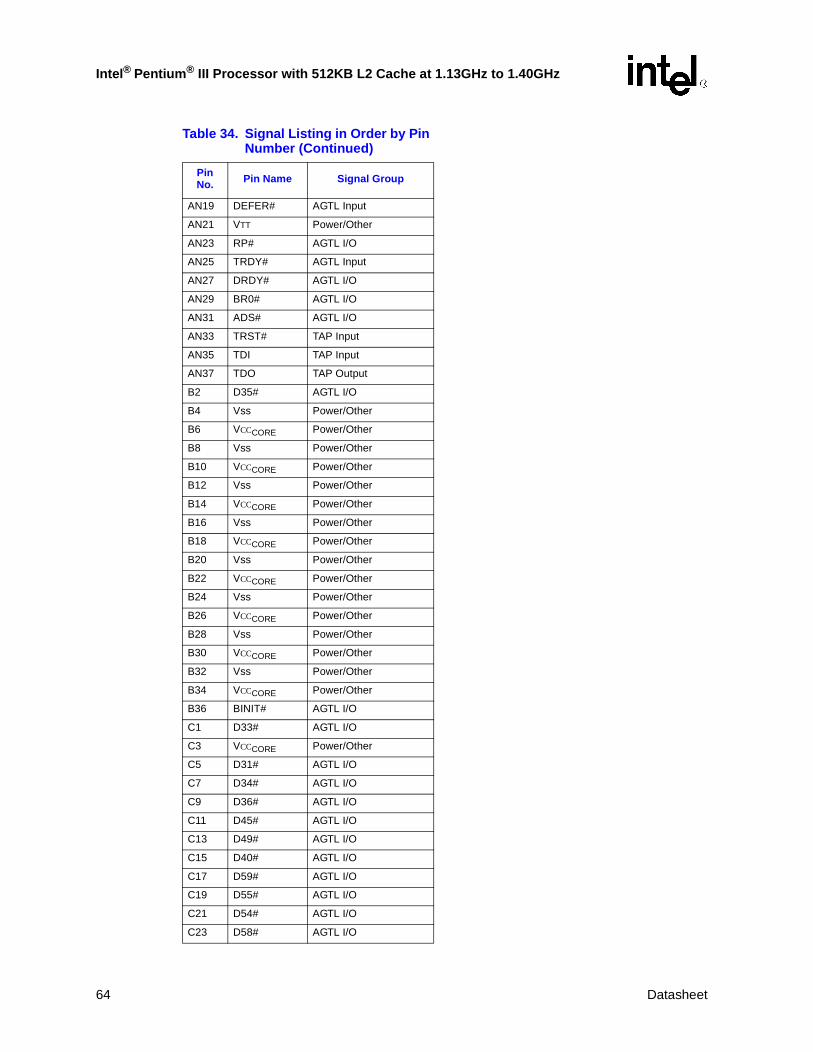
Intel® Pentium® III Processor with 512KB L2 Cache at 1.13GHz to 1.40GHz
AN19 DEFER# AGTL Input
AN21 VTT Power/Other
AN23 RP# AGTL I/O
AN25 TRDY# AGTL Input
AN27 DRDY# AGTL I/O
AN29 BR0# AGTL I/O
AN31 ADS# AGTL I/O
AN33 TRST# TAP Input
AN35 TDI TAP Input
AN37 TDO TAP Output
B2 D35# AGTL I/O
B4 Vss Power/Other
B6 VCCCORE Power/Other
B8 Vss Power/Other
B10 VCCCORE Power/Other
B12 Vss Power/Other
B14 VCCCORE Power/Other
B16 Vss Power/Other
B18 VCCCORE Power/Other
B20 Vss Power/Other
B22 VCCCORE Power/Other
B24 Vss Power/Other
B26 VCCCORE Power/Other
B28 Vss Power/Other
B30 VCCCORE Power/Other
B32 Vss Power/Other
B34 VCCCORE Power/Other
B36 BINIT# AGTL I/O
C1 D33# AGTL I/O
C3 VCCCORE Power/Other
C5 D31# AGTL I/O
C7 D34# AGTL I/O
C9 D36# AGTL I/O
C11 D45# AGTL I/O
C13 D49# AGTL I/O
C15 D40# AGTL I/O
C17 D59# AGTL I/O
C19 D55# AGTL I/O
C21 D54# AGTL I/O
C23 D58# AGTL I/O
Table 34. Signal Listing in Order by Pin Number (Continued)
Pin No. Pin Name Signal Group
64 Datasheet
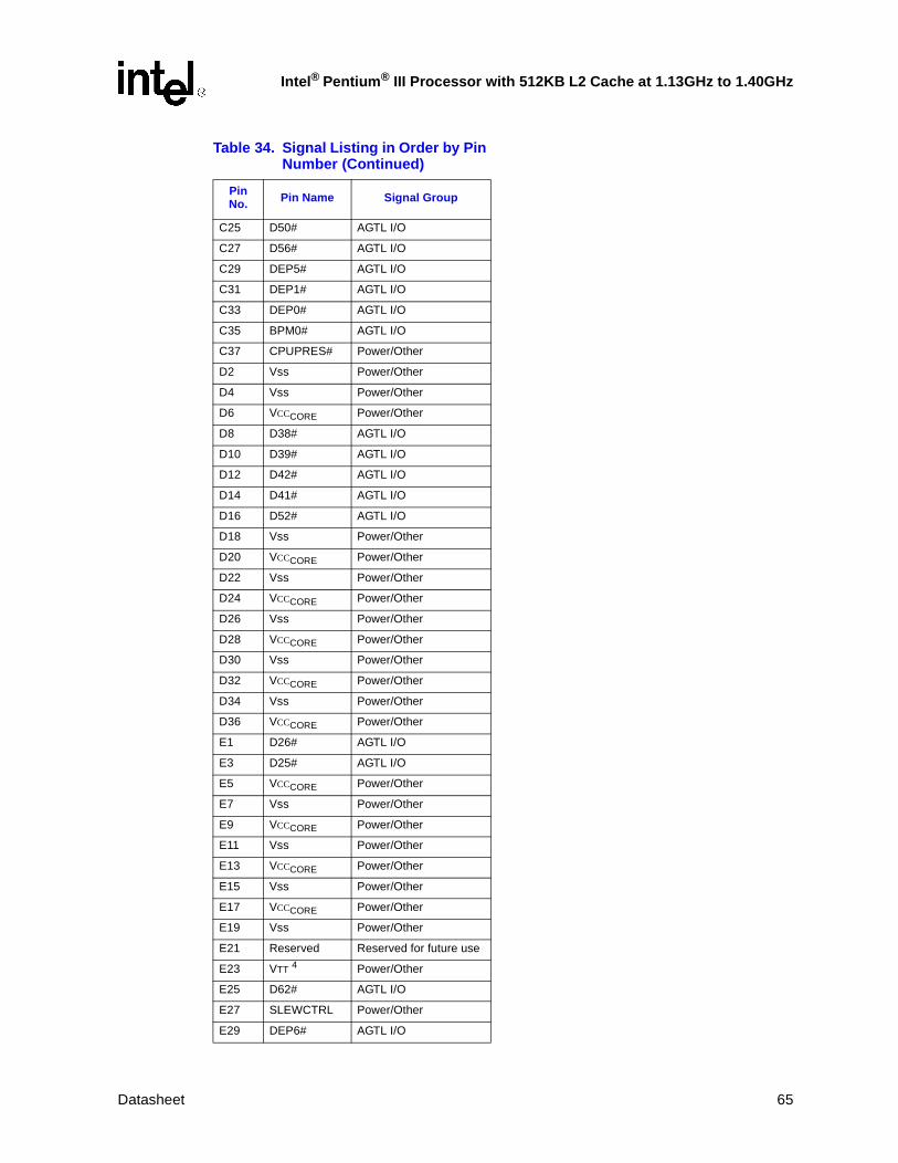
Intel® Pentium® III Processor with 512KB L2 Cache at 1.13GHz to 1.40GHz
C25 D50# AGTL I/O
C27 D56# AGTL I/O
C29 DEP5# AGTL I/O
C31 DEP1# AGTL I/O
C33 DEP0# AGTL I/O
C35 BPM0# AGTL I/O
C37 CPUPRES# Power/Other
D2 Vss Power/Other
D4 Vss Power/Other
D6 VCCCORE Power/Other
D8 D38# AGTL I/O
D10 D39# AGTL I/O
D12 D42# AGTL I/O
D14 D41# AGTL I/O
D16 D52# AGTL I/O
D18 Vss Power/Other
D20 VCCCORE Power/Other
D22 Vss Power/Other
D24 VCCCORE Power/Other
D26 Vss Power/Other
D28 VCCCORE Power/Other
D30 Vss Power/Other
D32 VCCCORE Power/Other
D34 Vss Power/Other
D36 VCCCORE Power/Other
E1 D26# AGTL I/O
E3 D25# AGTL I/O
E5 VCCCORE Power/Other
E7 Vss Power/Other
E9 VCCCORE Power/Other
E11 Vss Power/Other
E13 VCCCORE Power/Other
E15 Vss Power/Other
E17 VCCCORE Power/Other
E19 Vss Power/Other
E21 Reserved Reserved for future use
E23 VTT 4 Power/Other
E25 D62# AGTL I/O
E27 SLEWCTRL Power/Other
E29 DEP6# AGTL I/O
Table 34. Signal Listing in Order by Pin Number (Continued)
Pin No. Pin Name Signal Group
Datasheet 65
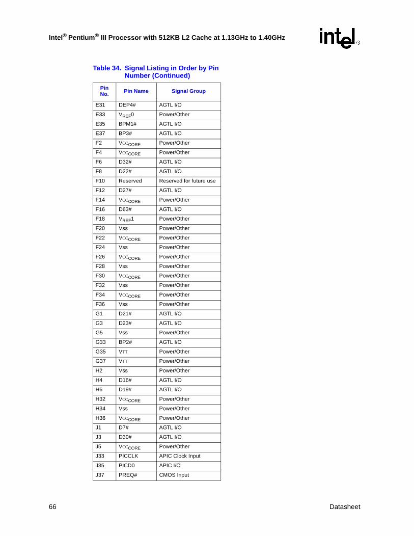
Intel® Pentium® III Processor with 512KB L2 Cache at 1.13GHz to 1.40GHz
E31 DEP4# AGTL I/O
E33 VREF0 Power/Other
E35 BPM1# AGTL I/O
E37 BP3# AGTL I/O
F2 VCCCORE Power/Other
F4 VCCCORE Power/Other
F6 D32# AGTL I/O
F8 D22# AGTL I/O
F10 Reserved Reserved for future use
F12 D27# AGTL I/O
F14 VCCCORE Power/Other
F16 D63# AGTL I/O
F18 VREF1 Power/Other
F20 Vss Power/Other
F22 VCCCORE Power/Other
F24 Vss Power/Other
F26 VCCCORE Power/Other
F28 Vss Power/Other
F30 VCCCORE Power/Other
F32 Vss Power/Other
F34 VCCCORE Power/Other
F36 Vss Power/Other
G1 D21# AGTL I/O
G3 D23# AGTL I/O
G5 Vss Power/Other
G33 BP2# AGTL I/O
G35 VTT Power/Other
G37 VTT Power/Other
H2 Vss Power/Other
H4 D16# AGTL I/O
H6 D19# AGTL I/O
H32 VCCCORE Power/Other
H34 Vss Power/Other
H36 VCCCORE Power/Other
J1 D7# AGTL I/O
J3 D30# AGTL I/O
J5 VCCCORE Power/Other
J33 PICCLK APIC Clock Input
J35 PICD0 APIC I/O
J37 PREQ# CMOS Input
Table 34. Signal Listing in Order by Pin Number (Continued)
Pin No. Pin Name Signal Group
66 Datasheet
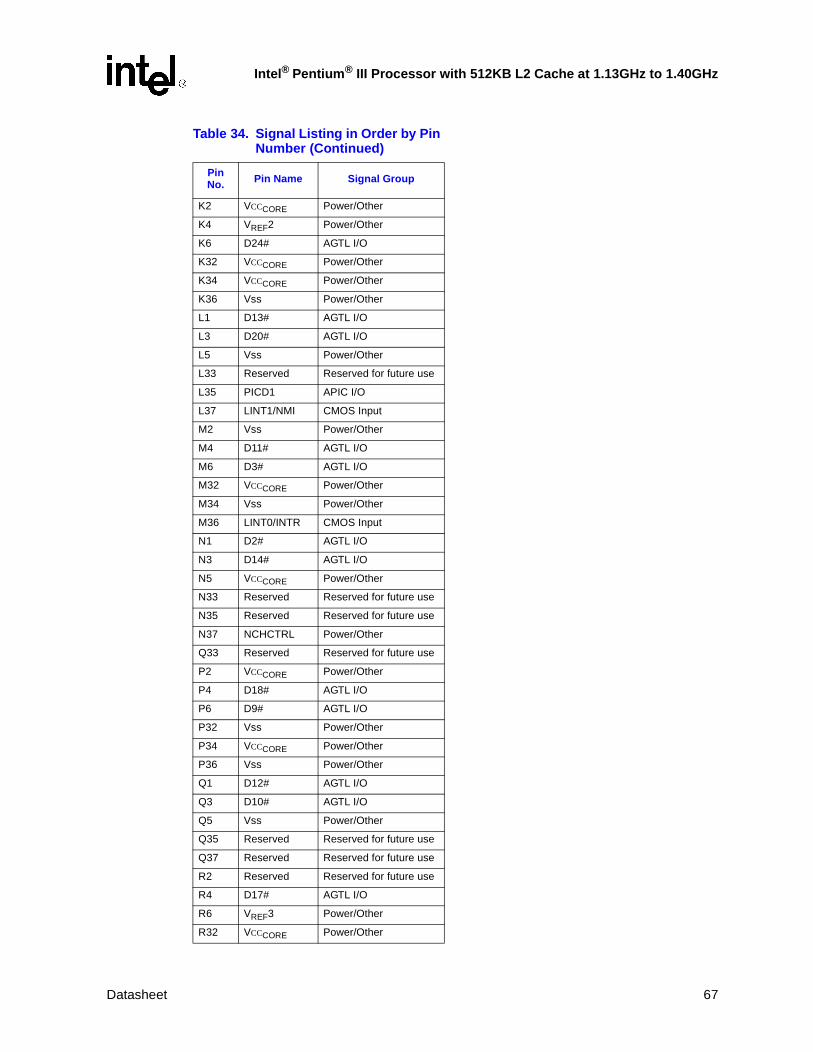
Intel® Pentium® III Processor with 512KB L2 Cache at 1.13GHz to 1.40GHz
K2 VCCCORE Power/Other
K4 VREF2 Power/Other
K6 D24# AGTL I/O
K32 VCCCORE Power/Other
K34 VCCCORE Power/Other
K36 Vss Power/Other
L1 D13# AGTL I/O
L3 D20# AGTL I/O
L5 Vss Power/Other
L33 Reserved Reserved for future use
L35 PICD1 APIC I/O
L37 LINT1/NMI CMOS Input
M2 Vss Power/Other
M4 D11# AGTL I/O
M6 D3# AGTL I/O
M32 VCCCORE Power/Other
M34 Vss Power/Other
M36 LINT0/INTR CMOS Input
N1 D2# AGTL I/O
N3 D14# AGTL I/O
N5 VCCCORE Power/Other
N33 Reserved Reserved for future use
N35 Reserved Reserved for future use
N37 NCHCTRL Power/Other
Q33 Reserved Reserved for future use
P2 VCCCORE Power/Other
P4 D18# AGTL I/O
P6 D9# AGTL I/O
P32 Vss Power/Other
P34 VCCCORE Power/Other
P36 Vss Power/Other
Q1 D12# AGTL I/O
Q3 D10# AGTL I/O
Q5 Vss Power/Other
Q35 Reserved Reserved for future use
Q37 Reserved Reserved for future use
R2 Reserved Reserved for future use
R4 D17# AGTL I/O
R6 VREF3 Power/Other
R32 VCCCORE Power/Other
Table 34. Signal Listing in Order by Pin Number (Continued)
Pin No. Pin Name Signal Group
Datasheet 67
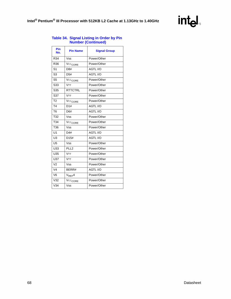
Intel® Pentium® III Processor with 512KB L2 Cache at 1.13GHz to 1.40GHz
R34 Vss Power/Other
R36 VCCCORE Power/Other
S1 D8# AGTL I/O
S3 D5# AGTL I/O
S5 VCCCORE Power/Other
S33 VTT Power/Other
S35 RTTCTRL Power/Other
S37 VTT Power/Other
T2 VCCCORE Power/Other
T4 D1# AGTL I/O
T6 D6# AGTL I/O
T32 Vss Power/Other
T34 VCCCORE Power/Other
T36 Vss Power/Other
U1 D4# AGTL I/O
U3 D15# AGTL I/O
U5 Vss Power/Other
U33 PLL2 Power/Other
U35 VTT Power/Other
U37 VTT Power/Other
V2 Vss Power/Other
V4 BERR# AGTL I/O
V6 VREF4 Power/Other
V32 VCCCORE Power/Other
V34 Vss Power/Other
Table 34. Signal Listing in Order by Pin Number (Continued)
Pin No. Pin Name Signal Group
68 Datasheet
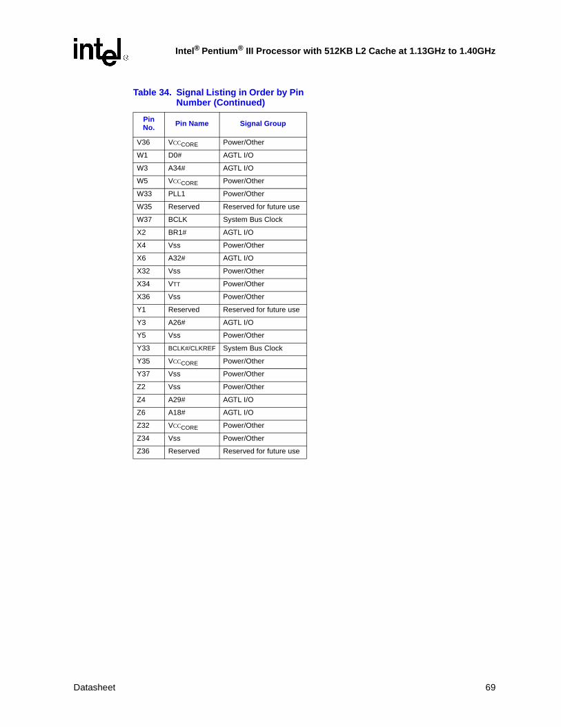
Intel® Pentium® III Processor with 512KB L2 Cache at 1.13GHz to 1.40GHz
V36 VCCCORE Power/Other
W1 D0# AGTL I/O
W3 A34# AGTL I/O
W5 VCCCORE Power/Other
W33 PLL1 Power/Other
W35 Reserved Reserved for future use
W37 BCLK System Bus Clock
X2 BR1# AGTL I/O
X4 Vss Power/Other
X6 A32# AGTL I/O
X32 Vss Power/Other
X34 VTT Power/Other
X36 Vss Power/Other
Y1 Reserved Reserved for future use
Y3 A26# AGTL I/O
Y5 Vss Power/Other
Y33 BCLK#/CLKREF System Bus Clock
Y35 VCCCORE Power/Other
Y37 Vss Power/Other
Z2 Vss Power/Other
Z4 A29# AGTL I/O
Z6 A18# AGTL I/O
Z32 VCCCORE Power/Other
Z34 Vss Power/Other
Z36 Reserved Reserved for future use
Table 34. Signal Listing in Order by Pin Number (Continued)
Pin No. Pin Name Signal Group
Datasheet 69
Intel® Pentium® III Processor with 512KB L2 Cache at 1.13GHz to 1.40GHz
6.0 Boxed Processor Specifications
The Intel® Pentium® III processor with 512KB L2 Cache for the PGA370 socket is also offered as an Intel® boxed processor. Intel® boxed processors are intended for system integrators who build systems from motherboards and standard components. The boxed Intel® Pentium® III processor with 512KB L2 Cache will be supplied with an unattached fan heatsink.
This section documents motherboard and system requirements for the fan heatsink that will be supplied with the boxed Intel® Pentium® III processor with 512KB L2 Cache. This section is particularly important for OEMs that manufacture motherboards for system integrators. Unless otherwise noted, all figures in this section are dimensioned in inches. Figure 28 shows a conceptual representation of the boxed Intel® Pentium® III processor with 512KB L2 Cache in the Flip Chip Pin Grid Array 2 (FC-PGA2) package.
Note: Drawings in this section reflect only the specifications on the Intel® Boxed Processor product. These dimensions should not be used as a generic keep-out zone for all heatsinks. It is the system designer’s responsibility to consider their proprietary solution when designing to the required keep-out zone on their system platform and chassis. Refer to the Intel® Pentium® III Processor Thermal/Mechanical Functional Specification for further guidance. Contact your local Intel Sales Representative for this document.
Figure 28. Conceptual Boxed Intel® Pentium® III Processor with 512KB L2 Cache for the PGA370 Socket
70 Datasheet

Intel® Pentium® III Processor with 512KB L2 Cache at 1.13GHz to 1.40GHz
6.1 Mechanical Specifications
6.1.1 Mechanical Specifications for the FC-PGA2 Package
This section documents the mechanical specifications of the boxed Intel® Pentium® III processor with 512KB L2 Cache fan heatsink in the FC-PGA2 Package. The boxed processor in the FC-PGA2 Package ships with an un-attached fan heatsink. Figure 28 shows a conceptual representation of the boxed Intel® Pentium® III processor with 512KB L2 Cache for the PGA370 socket in the Flip Chip Pin Grid Array 2 (FC-PGA2) package.
The boxed processor fan heatsink is also asymmetrical in that the mechanical step feature, Figure 31, must sit over the socket’s cam. The step allows the heatsink to securely interface with the processor in order to meet the processor’s thermal requirements.
The dimensions for the boxed processor with the integrated fan heatsink are shown in Figure 30. All dimensions are in inches.
The Intel® Pentium® III processor with 512KB L2 Cache uses a new technology termed FC-PGA2. The FC-PGA2 package leverages the previous FC-PGA package technology used on legacy Pentium® III processors. The FC-PGA2 package adds an Integrated Heat Spreader (IHS) to improve heat conduction from the processor die. This new solution prevent the need for exotic thermal solutions in the higher power density processors. See section 5.0 of this document for the mechanical specifications of the PGA370 socket.
Section 5.2 of this document also shows the recommended mechanical keepout zones for the boxed processor fan heatsink assembly. Figure 24 and Figure 25 show the REQUIRED keepout dimensions for the boxed processor thermal solution. The cooling fin orientation on the heatsink relative to the PGA370 socket is subject to change. Contact your local Intel Sales Representative for documentation specific to the boxed fan heatsink orientation relative to the PGA370 socket.
Figure 31 shows the changes to the package mechanicals between the FC-PGA and FC-PGA2 designs. Note that the boxed fan heatsinks and associated clips are not compatible with earlier boxed Intel® Pentium® III processor fan heatsinks.
Figure 29. Comparison between FC-PGA and FC-PGA2 package
Datasheet 71
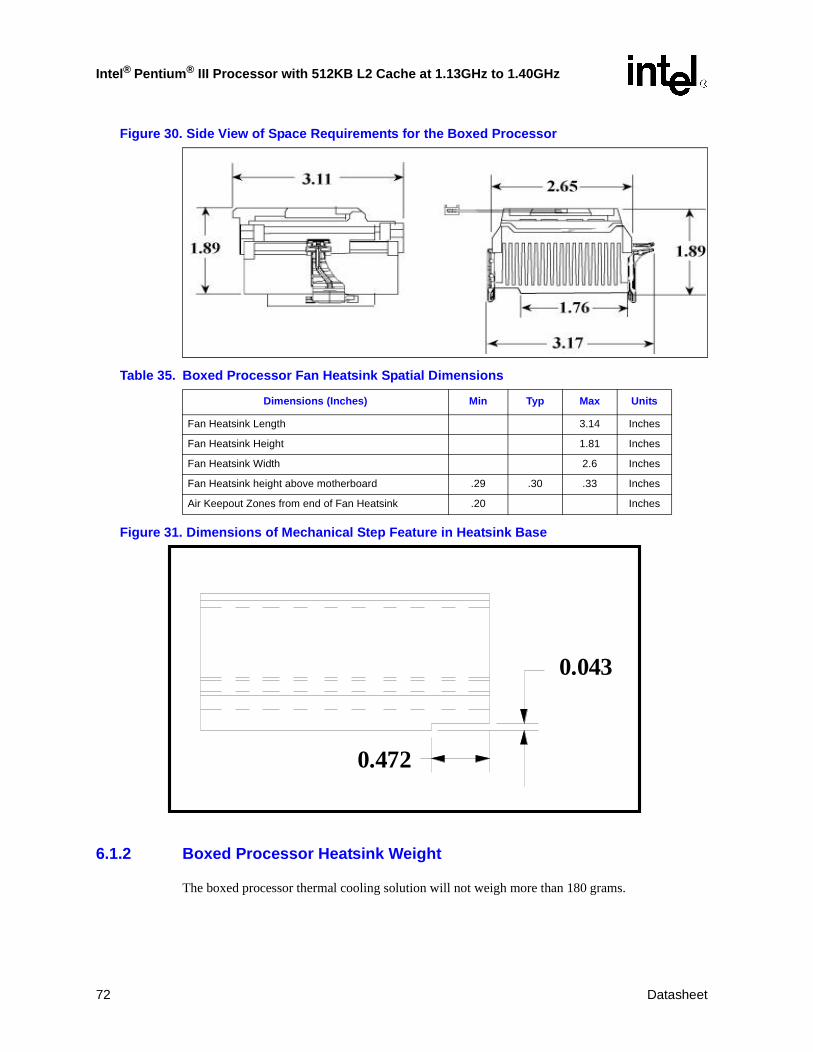
Intel® Pentium® III Processor with 512KB L2 Cache at 1.13GHz to 1.40GHz
Figure 31. Dimensions of Mechanical Step Feature in Heatsink Base
6.1.2 Boxed Processor Heatsink Weight
The boxed processor thermal cooling solution will not weigh more than 180 grams.
Figure 30. Side View of Space Requirements for the Boxed Processor
Table 35. Boxed Processor Fan Heatsink Spatial Dimensions
Dimensions (Inches) Min Typ Max Units
Fan Heatsink Length 3.14 Inches
Fan Heatsink Height 1.81 Inches
Fan Heatsink Width 2.6 Inches
Fan Heatsink height above motherboard .29 .30 .33 Inches
Air Keepout Zones from end of Fan Heatsink .20 Inches
0.043
0.472
72 Datasheet
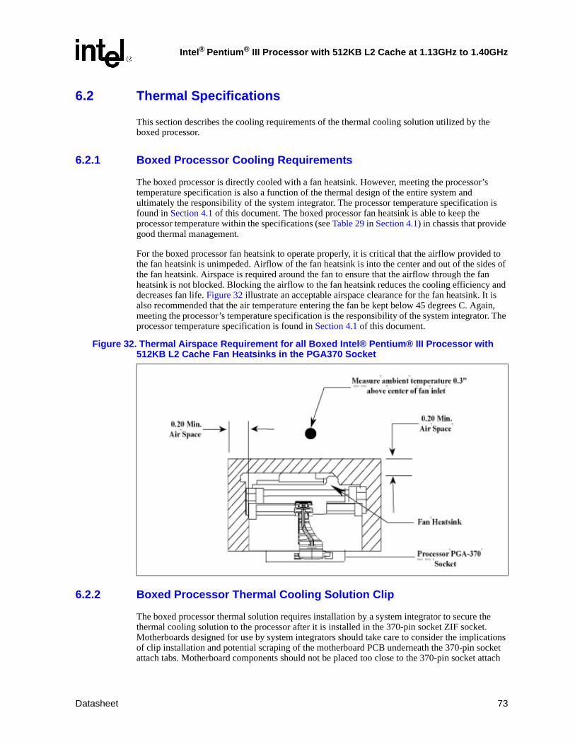
Intel® Pentium® III Processor with 512KB L2 Cache at 1.13GHz to 1.40GHz
6.2 Thermal Specifications
This section describes the cooling requirements of the thermal cooling solution utilized by the boxed processor.
6.2.1 Boxed Processor Cooling Requirements
The boxed processor is directly cooled with a fan heatsink. However, meeting the processor’s temperature specification is also a function of the thermal design of the entire system and ultimately the responsibility of the system integrator. The processor temperature specification is found in Section 4.1 of this document. The boxed processor fan heatsink is able to keep the processor temperature within the specifications (see Table 29 in Section 4.1) in chassis that provide good thermal management.
For the boxed processor fan heatsink to operate properly, it is critical that the airflow provided to the fan heatsink is unimpeded. Airflow of the fan heatsink is into the center and out of the sides of the fan heatsink. Airspace is required around the fan to ensure that the airflow through the fan heatsink is not blocked. Blocking the airflow to the fan heatsink reduces the cooling efficiency and decreases fan life. Figure 32 illustrate an acceptable airspace clearance for the fan heatsink. It is also recommended that the air temperature entering the fan be kept below 45 degrees C. Again, meeting the processor’s temperature specification is the responsibility of the system integrator. The processor temperature specification is found in Section 4.1 of this document.
6.2.2 Boxed Processor Thermal Cooling Solution Clip
The boxed processor thermal solution requires installation by a system integrator to secure the thermal cooling solution to the processor after it is installed in the 370-pin socket ZIF socket. Motherboards designed for use by system integrators should take care to consider the implications of clip installation and potential scraping of the motherboard PCB underneath the 370-pin socket attach tabs. Motherboard components should not be placed too close to the 370-pin socket attach
Figure 32. Thermal Airspace Requirement for all Boxed Intel® Pentium® III Processor with 512KB L2 Cache Fan Heatsinks in the PGA370 Socket
Datasheet 73
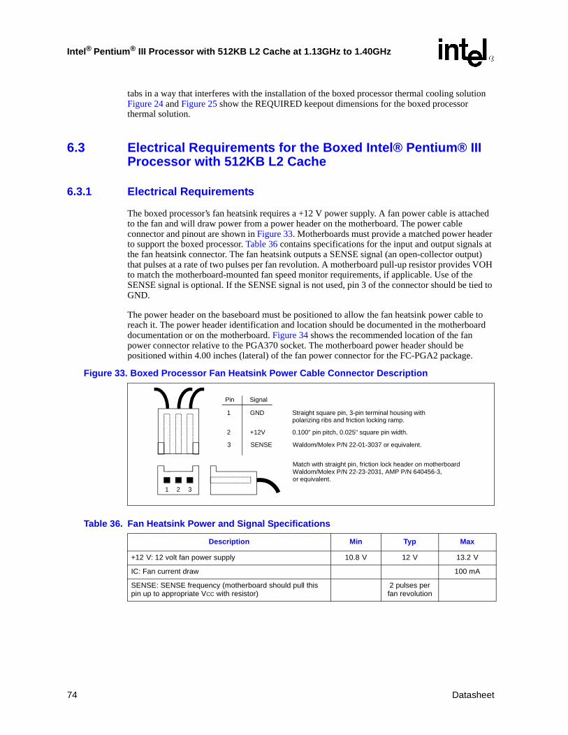
Intel® Pentium® III Processor with 512KB L2 Cache at 1.13GHz to 1.40GHz
tabs in a way that interferes with the installation of the boxed processor thermal cooling solution Figure 24 and Figure 25 show the REQUIRED keepout dimensions for the boxed processor thermal solution.
6.3 Electrical Requirements for the Boxed Intel® Pentium® III Processor with 512KB L2 Cache
6.3.1 Electrical Requirements
The boxed processor’s fan heatsink requires a +12 V power supply. A fan power cable is attached to the fan and will draw power from a power header on the motherboard. The power cable connector and pinout are shown in Figure 33. Motherboards must provide a matched power header to support the boxed processor. Table 36 contains specifications for the input and output signals at the fan heatsink connector. The fan heatsink outputs a SENSE signal (an open-collector output) that pulses at a rate of two pulses per fan revolution. A motherboard pull-up resistor provides VOH to match the motherboard-mounted fan speed monitor requirements, if applicable. Use of the SENSE signal is optional. If the SENSE signal is not used, pin 3 of the connector should be tied to GND.
The power header on the baseboard must be positioned to allow the fan heatsink power cable to reach it. The power header identification and location should be documented in the motherboard documentation or on the motherboard. Figure 34 shows the recommended location of the fan power connector relative to the PGA370 socket. The motherboard power header should be positioned within 4.00 inches (lateral) of the fan power connector for the FC-PGA2 package.
Figure 33. Boxed Processor Fan Heatsink Power Cable Connector Description
Table 36. Fan Heatsink Power and Signal Specifications
Description Min Typ Max
+12 V: 12 volt fan power supply 10.8 V 12 V 13.2 V
IC: Fan current draw 100 mA
SENSE: SENSE frequency (motherboard should pull this pin up to appropriate VCC with resistor)
2 pulses per fan revolution
Pin Signal
Straight square pin, 3-pin terminal housing withpolarizing ribs and friction locking ramp.
0.100" pin pitch, 0.025" square pin width.
Waldom/Molex P/N 22-01-3037 or equivalent.
Match with straight pin, friction lock header on motherboardWaldom/Molex P/N 22-23-2031, AMP P/N 640456-3,or equivalent.
1
2
3
GND
+12V
SENSE
1 2 3
74 Datasheet
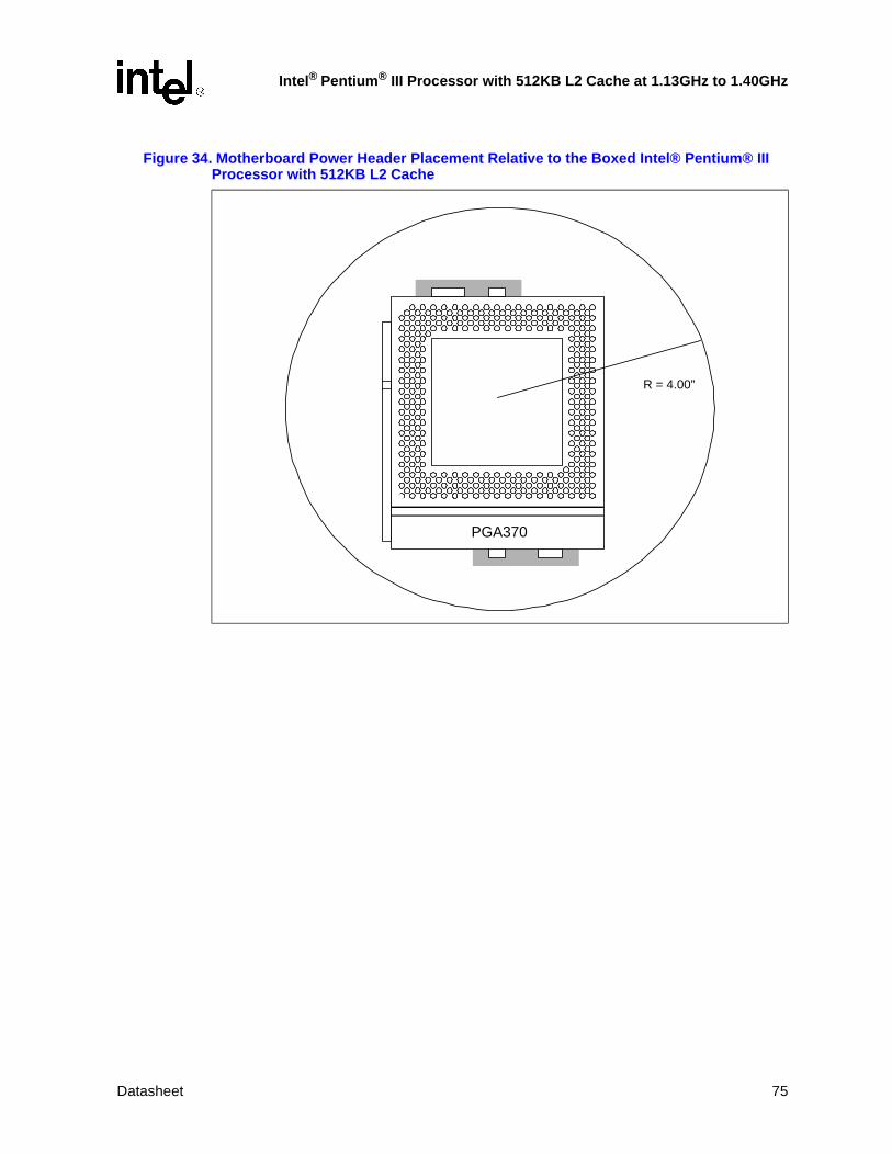
Intel® Pentium® III Processor with 512KB L2 Cache at 1.13GHz to 1.40GHz
Figure 34. Motherboard Power Header Placement Relative to the Boxed Intel® Pentium® III Processor with 512KB L2 Cache
0.10"
Socket 7
0.10"
R = 4.00”
PGA370
Datasheet 75
Intel® Pentium® III Processor with 512KB L2 Cache at 1.13GHz to 1.40GHz
7.0 Processor Signal Description
This section provides an alphabetical listing of all the Intel® Pentium® III processor with 512 KB L2 Cache signals. The tables at the end of this section summarize the signals by direction: output, input, and I/O.
7.1 Alphabetical Signals Reference
Table 37. Signal Description (Sheet 1 of 9)
Name Type Description
A20M# I
If the A20M# (Address-20 Mask) input signal is asserted, the processor masks physical address bit 20 (A20#) before looking up a line in any internal cache and before driving a read/write transaction on the bus. Asserting A20M# emulates the 8086 processor’s address wrap-around at the 1MB boundary. Assertion of A20M# is only supported in real mode.
A20M# is an asynchronous signal. However, to ensure recognition of this signal following an I/O write instruction, it must be valid along with the TRDY# assertion of the corresponding I/O Write bus transaction.
A[35:3]# I/O
The A[35:3]# (Address) signals define a 236-byte physical memory address space. When ADS# is active, these pins transmit the address of a transaction; when ADS# is inactive, these pins transmit transaction type information. These signals must connect the appropriate pins of all agents on the processor system bus. The A[35:24]# signals are parity-protected by the AP1# parity signal, and the A[23:3]# signals are parity-protected by the AP0# parity signal.
On the active-to-inactive transition of RESET#, the processors sample the A[35:3]# pins to determine their power-on configuration. See the Intel® Pentium® II Processor Developer’s Manual for details.
ADS# I/O
The ADS# (Address Strobe) signal is asserted to indicate the validity of the transaction address on the A[35:3]# pins. All bus agents observe the ADS# activation to begin parity checking, protocol checking, address decode, internal snoop, or deferred reply ID match operations associated with the new transaction. This signal must connect the appropriate pins on all processor system bus agents.
AERR# I/O
The AERR# (Address Parity Error) signal is observed and driven by all processor system bus agents, and if used, must connect the appropriate pins on all processor system bus agents. AERR# observation is optionally enabled during power-on configuration; if enabled, a valid assertion of AERR# aborts the current transaction.
If AERR# observation is disabled during power-on configuration, a central agent may handle an assertion of AERR# as appropriate to the error handling architecture of the system.
AP[1:0]# I/O
The AP[1:0]# (Address Parity) signals are driven by the request initiator along with ADS#, A[35:3]#, REQ[4:0]#, and RP#. AP1# covers A[35:24]#, and AP0# covers A[23:3]#. A correct parity signal is high if an even number of covered signals are low and low if an odd number of covered signals are low. This allows parity to be high when all the covered signals are high. AP[1:0]# should connect the appropriate pins of all processor system bus agents.
BCLK/BCLK# I
The BCLK (Bus Clock) and BCLK# (for differential clock) signals determines the bus frequency. All processor system bus agents must receive this signal to drive their outputs and latch their inputs on the rising edge of BCLK. For differential clocking, all processor system bus agents must receive this signal to drive their outputs and latch their inputs on the BCLK and BCLK# crossing point.
All external timing parameters are specified with respect to the BCLK signal.
76 Datasheet
Intel® Pentium® III Processor with 512KB L2 Cache at 1.13GHz to 1.40GHz
BERR# I/O
The BERR# (Bus Error) signal is asserted to indicate an unrecoverable error without a bus protocol violation. It may be driven by all processor system bus agents, and must connect the appropriate pins of all such agents, if used. However, Intel® Pentium® III processors do not observe assertions of the BERR# signal.
BERR# assertion conditions are configurable at a system level. Assertion options are defined by the following options:
• Enabled or disabled.
• Asserted optionally for internal errors along with IERR#.
• Asserted optionally by the request initiator of a bus transaction after it observes an error.
• Asserted by any bus agent when it observes an error in a bus transaction.
BINIT# I/O
The BINIT# (Bus Initialization) signal may be observed and driven by all processor system bus agents, and if used must connect the appropriate pins of all such agents. If the BINIT# driver is enabled during power on configuration, BINIT# is asserted to signal any bus condition that prevents reliable future information.
If BINIT# observation is enabled during power-on configuration, and BINIT# is sampled asserted, all bus state machines are reset and any data which was in transit is lost. All agents reset their rotating ID for bus arbitration to the state after Reset, and internal count information is lost. The L1 and L2 caches are not affected.
If BINIT# observation is disabled during power-on configuration, a central agent may handle an assertion of BINIT# as appropriate to the error handling architecture of the system.
BNR# I/O
The BNR# (Block Next Request) signal is used to assert a bus stall by any bus agent who is unable to accept new bus transactions. During a bus stall, the current bus owner cannot issue any new transactions.
Since multiple agents might need to request a bus stall at the same time, BNR# is a wire-OR signal which must connect the appropriate pins of all processor system bus agents. In order to avoid wire-OR glitches associated with simultaneous edge transitions driven by multiple drivers, BNR# is activated on specific clock edges and sampled on specific clock edges.
BP[3:2]# I/O The BP[3:2]# (Breakpoint) signals are outputs from the processor that indicate the status of breakpoints.
BPM[1:0]# I/O
The BPM[1:0]# (Breakpoint Monitor) signals are breakpoint and performance monitor signals. They are outputs from the processor which indicate the status of breakpoints and programmable counters used for monitoring processor performance.
BPRI# I
The BPRI# (Bus Priority Request) signal is used to arbitrate for ownership of the processor system bus. It must connect the appropriate pins of all processor system bus agents. Observing BPRI# active (as asserted by the priority agent) causes all other agents to stop issuing new requests, unless such requests are part of an ongoing locked operation. The priority agent keeps BPRI# asserted until all of its requests are completed, then releases the bus by deasserting BPRI#.
Table 37. Signal Description (Sheet 2 of 9)
Name Type Description
Datasheet 77
Intel® Pentium® III Processor with 512KB L2 Cache at 1.13GHz to 1.40GHz
BR0#/BR1# I/O
The BR0# and BR1#(Bus Request) pins drive the BREQ[1:0]# signals in the system. The BREQ[1:0]# signals are interconnected in a rotating manner to individual processor pins. The table below gives the rotating interconnect between the processor and bus signals.
During power-up configuration, the central agent asserts the BR0# bus signal in the system to assign the symmetric agent ID to the processor. The processor samples its BR0# pin on the active-to-inactive transition of the RESET# to obtain its symmetric agent ID. The processor asserts the BR0# pin to request the system bus. All agents then configure their pins to match the appropriate bus signal protocol, as shown below.
For uni-processor designs, BR0# must be connected to a 10-56Ω resistor to VSS. Refer to the platform design guide for implementation detail and resistor tolerance.
BSEL[1:0] O
The BSEL signals are CMOS signals which are used to select the system bus frequency. A BSEL[1:0] = ‘11’ selects a 133 MHz system bus frequency. The frequency is determined by the processor(s), chipset, and frequency synthesizer capabilities. All system bus agents must operate at the same frequency. The Intel® Pentium® III processor with 512KB L2 Cache operates at 133 MHz system bus frequency. These signals must be pulled up to 3.3V power rail with 330 - 1 KΩ resistors and provided as a frequency selection signal to the clock driver/synthesizer and chipset. Refer to the platform design guide for implementation detail and resistor tolerance.
CLKREF I
In Single-ended clock mode the CLKREF input is a filtered 1.25V supply voltage for the processor PLL. A voltage divider and decoupling solution is provided by the motherboard. See the design guide for implementation details.
When the processor operates in differential clock mode, this signal becomes BCLK#.
Table 37. Signal Description (Sheet 3 of 9)
Name Type Description
BR0# (I/O) and BR1# Signals Rotating Interconnect
Bus Signal Agent 0 Pins Agent 1 Pins
BREQ0# BR0# BR1#
BREQ1# BR1# BR0#
BR0# (I/O) and BR1# Signals Rotating Interconnect
Pin Sampled Active in RESET# Agent ID
BR0# 0
BR1# 3
78 Datasheet
Intel® Pentium® III Processor with 512KB L2 Cache at 1.13GHz to 1.40GHz
CPUPRES# O
The CPUPRES# signal is defined to allow a system design to detect the presence of a terminator device or processor in a PGA370 socket. Combined with the VID combination of VID[25mV,3:0]= 11111 (see Section 2.6), a system can determine if a socket is occupied, and whether a processor core is present. See the table below for states and values for determining the presence of a device.
D[63:0]# I/O
The D[63:0]# (Data) signals are the data signals. These signals provide a 64-bit data path between the processor system bus agents, and must connect the appropriate pins on all such agents. The data driver asserts DRDY# to indicate a valid data transfer.
DBSY# I/O
The DBSY# (Data Bus Busy) signal is asserted by the agent responsible for driving data on the processor system bus to indicate that the data bus is in use. The data bus is released after DBSY# is deasserted. This signal must connect the appropriate pins on all processor system bus agents.
DEFER# I
The DEFER# signal is asserted by an agent to indicate that a transaction cannot be guaranteed in-order completion. Assertion of DEFER# is normally the responsibility of the addressed memory or I/O agent. This signal must connect the appropriate pins of all processor system bus agents.
DEP[7:0]# I/O
The DEP[7:0]# (Data Bus ECC Protection) signals provide optional ECC protection for the data bus. They are driven by the agent responsible for driving D[63:0]#, and must connect the appropriate pins of all processor system bus agents which use them. The DEP[7:0]# signals are enabled or disabled for ECC protection during power on configuration.
DETECT O
A tri-state (high-impedance) output. Can be used for platforms that need to differentiate Intel® Pentium® III processors with 512KB L2 Cache that support VTT=1.25V only, from Pentium® III processors (AF36=VSS) that support VTT=1.50V only. The output on this signal is stable when VTT is stable. Please refer to the appropriate Platform Design Guide for implementation details.
DRDY# I/O
The DRDY# (Data Ready) signal is asserted by the data driver on each data transfer, indicating valid data on the data bus. In a multi-cycle data transfer, DRDY# may be deasserted to insert idle clocks. This signal must connect the appropriate pins of all processor system bus agents.
DYN_OE I
The DYN_OE allows the BSEL and VID signals to be driven out from the processor. When this signal is low (a condition that will occur if the Intel® Pentium® III processor is installed in a non-supported platform), the VID and BSEL signals will be tri-stated and the platform pull-up resistors will set the VID and BSEL to all ‘1’s’ which is a safe setting. This signal must be connected to a 1kΩ resistor to VTT. Refer to the platform design guide for implementation detail and resistor tolerance.
FERR# O
The FERR# (Floating-point Error) signal is asserted when the processor detects an unmasked floating-point error. FERR# is similar to the ERROR# signal on the Intel 387 coprocessor, and is included for compatibility with systems using MS-DOS*-type floating-point error reporting.
Table 37. Signal Description (Sheet 4 of 9)
Name Type Description
PGA370 Socket Occupation Truth Table
Signal Value Status
CPUPRES#VID[25mV,3:0]
0Anything other than ‘11111’
Processor core installed in the PGA370 socket.
CPUPRES#VID[25mV,3:0]
011111
Terminator device installed in the PGA370 socket (i.e., no core present).
CPUPRES#VID[25mV,3:0]
1Any value PGA370 socket not occupied.
Datasheet 79
Intel® Pentium® III Processor with 512KB L2 Cache at 1.13GHz to 1.40GHz
FLUSH# I
When the FLUSH# input signal is asserted, processors write back all data in the Modified state from their internal caches and invalidate all internal cache lines. At the completion of this operation, the processor issues a Flush Acknowledge transaction. The processor does not cache any new data while the FLUSH# signal remains asserted.
FLUSH# is an asynchronous signal. However, to ensure recognition of this signal following an I/O write instruction, it must be valid along with the TRDY# assertion of the corresponding I/O Write bus transaction.
On the active-to-inactive transition of RESET#, each processor samples FLUSH# to determine its power-on configuration. See the P6 Family of Processors Hardware Developer’s Manual for details.
This signal must be connected to a 150ohm resistor to VCCCMOS1.5. Refer to the platform design guide for implementation detail and resistor tolerance.
HIT#
HITM#
I/O
I/O
The HIT# (Snoop Hit) and HITM# (Hit Modified) signals convey transaction snoop operation results, and must connect the appropriate pins of all processor system bus agents. Any such agent may assert both HIT# and HITM# together to indicate that it requires a snoop stall, which can be continued by reasserting HIT# and HITM# together.
IERR# O
The IERR# (Internal Error) signal is asserted by a processor as the result of an internal error. Assertion of IERR# is usually accompanied by a SHUTDOWN transaction on the processor system bus. This transaction may optionally be converted to an external error signal (e.g., NMI) by system core logic. The processor will keep IERR# asserted until the assertion of RESET#, BINIT#, or INIT#.
IGNNE# I
The IGNNE# (Ignore Numeric Error) signal is asserted to force the processor to ignore a numeric error and continue to execute noncontrol floating-point instructions. If IGNNE# is deasserted, the processor generates an exception on a noncontrol floating-point instruction if a previous floating-point instruction caused an error. IGNNE# has no effect when the NE bit in control register 0 is set.
IGNNE# is an asynchronous signal. However, to ensure recognition of this signal following an I/O write instruction, it must be valid along with the TRDY# assertion of the corresponding I/O Write bus transaction.
INIT# I
The INIT# (Initialization) signal, when asserted, resets integer registers inside all processors without affecting their internal (L1 or L2) caches or floating-point registers. Each processor then begins execution at the power-on Reset vector configured during power-on configuration. The processor continues to handle snoop requests during INIT# assertion. INIT# is an asynchronous signal and must connect the appropriate pins of all processor system bus agents.
If INIT# is sampled active on the active to inactive transition of RESET#, then the processor executes its Built-in Self-Test (BIST).
KEY I
Can be used to prevent legacy processors from booting in incompatible platforms. Legacy processors use this pin as a RESET and should be tied to ground for an Intel® Pentium® III processor with 512KB L2 Cache only platform, but for flexible platform implementations this pin should be a No Connect. Please refer to the appropriate Platform Design Guide for implementation details.
LINT[1:0] I
The LINT[1:0] (Local APIC Interrupt) signals must connect the appropriate pins of all APIC Bus agents, including all processors and the core logic or I/O APIC component. When the APIC is disabled, the LINT0 signal becomes INTR, a maskable interrupt request signal, and LINT1 becomes NMI, a nonmaskable interrupt. INTR and NMI are backward compatible with the signals of those names on the Intel® Pentium® processor. Both signals are asynchronous.
Both of these signals must be software configured via BIOS programming of the APIC register space to be used either as NMI/INTR or LINT[1:0]. Because the APIC is enabled by default after Reset, operation of these pins as LINT[1:0] is the default configuration.
Table 37. Signal Description (Sheet 5 of 9)
Name Type Description
80 Datasheet
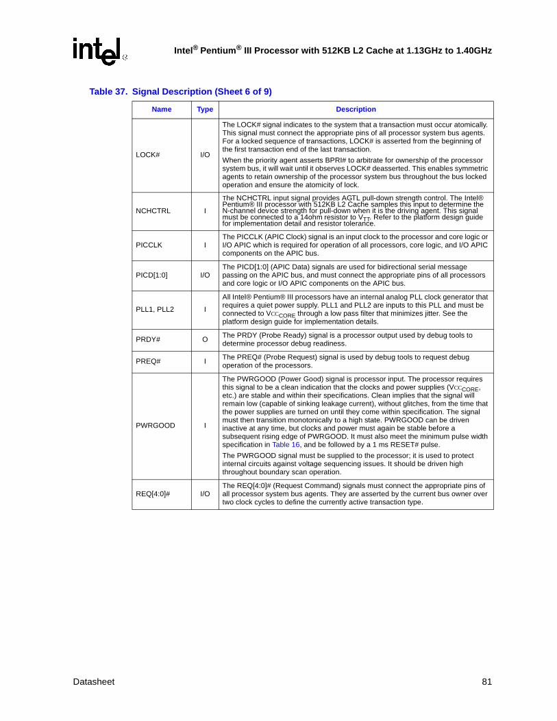
Intel® Pentium® III Processor with 512KB L2 Cache at 1.13GHz to 1.40GHz
LOCK# I/O
The LOCK# signal indicates to the system that a transaction must occur atomically. This signal must connect the appropriate pins of all processor system bus agents. For a locked sequence of transactions, LOCK# is asserted from the beginning of the first transaction end of the last transaction.
When the priority agent asserts BPRI# to arbitrate for ownership of the processor system bus, it will wait until it observes LOCK# deasserted. This enables symmetric agents to retain ownership of the processor system bus throughout the bus locked operation and ensure the atomicity of lock.
NCHCTRL I
The NCHCTRL input signal provides AGTL pull-down strength control. The Intel® Pentium® III processor with 512KB L2 Cache samples this input to determine the N-channel device strength for pull-down when it is the driving agent. This signal must be connected to a 14ohm resistor to VTT. Refer to the platform design guide for implementation detail and resistor tolerance.
PICCLK IThe PICCLK (APIC Clock) signal is an input clock to the processor and core logic or I/O APIC which is required for operation of all processors, core logic, and I/O APIC components on the APIC bus.
PICD[1:0] I/OThe PICD[1:0] (APIC Data) signals are used for bidirectional serial message passing on the APIC bus, and must connect the appropriate pins of all processors and core logic or I/O APIC components on the APIC bus.
PLL1, PLL2 I
All Intel® Pentium® III processors have an internal analog PLL clock generator that requires a quiet power supply. PLL1 and PLL2 are inputs to this PLL and must be connected to VCCCORE through a low pass filter that minimizes jitter. See the platform design guide for implementation details.
PRDY# O The PRDY (Probe Ready) signal is a processor output used by debug tools to determine processor debug readiness.
PREQ# I The PREQ# (Probe Request) signal is used by debug tools to request debug operation of the processors.
PWRGOOD I
The PWRGOOD (Power Good) signal is processor input. The processor requires this signal to be a clean indication that the clocks and power supplies (VCCCORE, etc.) are stable and within their specifications. Clean implies that the signal will remain low (capable of sinking leakage current), without glitches, from the time that the power supplies are turned on until they come within specification. The signal must then transition monotonically to a high state. PWRGOOD can be driven inactive at any time, but clocks and power must again be stable before a subsequent rising edge of PWRGOOD. It must also meet the minimum pulse width specification in Table 16, and be followed by a 1 ms RESET# pulse.
The PWRGOOD signal must be supplied to the processor; it is used to protect internal circuits against voltage sequencing issues. It should be driven high throughout boundary scan operation.
REQ[4:0]# I/OThe REQ[4:0]# (Request Command) signals must connect the appropriate pins of all processor system bus agents. They are asserted by the current bus owner over two clock cycles to define the currently active transaction type.
Table 37. Signal Description (Sheet 6 of 9)
Name Type Description
Datasheet 81
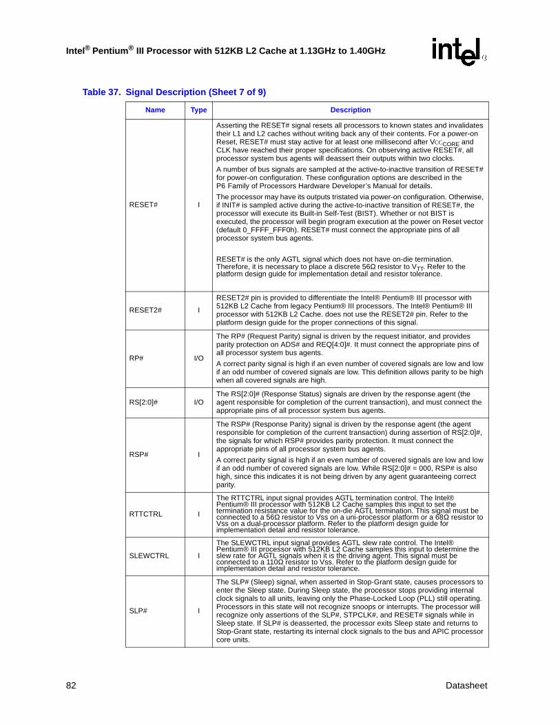
Intel® Pentium® III Processor with 512KB L2 Cache at 1.13GHz to 1.40GHz
RESET# I
Asserting the RESET# signal resets all processors to known states and invalidates their L1 and L2 caches without writing back any of their contents. For a power-on Reset, RESET# must stay active for at least one millisecond after VCCCORE and CLK have reached their proper specifications. On observing active RESET#, all processor system bus agents will deassert their outputs within two clocks.
A number of bus signals are sampled at the active-to-inactive transition of RESET# for power-on configuration. These configuration options are described in the P6 Family of Processors Hardware Developer’s Manual for details.
The processor may have its outputs tristated via power-on configuration. Otherwise, if INIT# is sampled active during the active-to-inactive transition of RESET#, the processor will execute its Built-in Self-Test (BIST). Whether or not BIST is executed, the processor will begin program execution at the power on Reset vector (default 0_FFFF_FFF0h). RESET# must connect the appropriate pins of all processor system bus agents.
RESET# is the only AGTL signal which does not have on-die termination. Therefore, it is necessary to place a discrete 56Ω resistor to VTT. Refer to the platform design guide for implementation detail and resistor tolerance.
RESET2# I
RESET2# pin is provided to differentiate the Intel® Pentium® III processor with 512KB L2 Cache from legacy Pentium® III processors. The Intel® Pentium® III processor with 512KB L2 Cache. does not use the RESET2# pin. Refer to the platform design guide for the proper connections of this signal.
RP# I/O
The RP# (Request Parity) signal is driven by the request initiator, and provides parity protection on ADS# and REQ[4:0]#. It must connect the appropriate pins of all processor system bus agents.
A correct parity signal is high if an even number of covered signals are low and low if an odd number of covered signals are low. This definition allows parity to be high when all covered signals are high.
RS[2:0]# I/OThe RS[2:0]# (Response Status) signals are driven by the response agent (the agent responsible for completion of the current transaction), and must connect the appropriate pins of all processor system bus agents.
RSP# I
The RSP# (Response Parity) signal is driven by the response agent (the agent responsible for completion of the current transaction) during assertion of RS[2:0]#, the signals for which RSP# provides parity protection. It must connect the appropriate pins of all processor system bus agents.
A correct parity signal is high if an even number of covered signals are low and low if an odd number of covered signals are low. While RS[2:0]# = 000, RSP# is also high, since this indicates it is not being driven by any agent guaranteeing correct parity.
RTTCTRL I
The RTTCTRL input signal provides AGTL termination control. The Intel® Pentium® III processor with 512KB L2 Cache samples this input to set the termination resistance value for the on-die AGTL termination. This signal must be connected to a 56Ω resistor to Vss on a uni-processor platform or a 68Ω resistor to Vss on a dual-processor platform. Refer to the platform design guide for implementation detail and resistor tolerance.
SLEWCTRL I
The SLEWCTRL input signal provides AGTL slew rate control. The Intel® Pentium® III processor with 512KB L2 Cache samples this input to determine the slew rate for AGTL signals when it is the driving agent. This signal must be connected to a 110Ω resistor to Vss. Refer to the platform design guide for implementation detail and resistor tolerance.
SLP# I
The SLP# (Sleep) signal, when asserted in Stop-Grant state, causes processors to enter the Sleep state. During Sleep state, the processor stops providing internal clock signals to all units, leaving only the Phase-Locked Loop (PLL) still operating. Processors in this state will not recognize snoops or interrupts. The processor will recognize only assertions of the SLP#, STPCLK#, and RESET# signals while in Sleep state. If SLP# is deasserted, the processor exits Sleep state and returns to Stop-Grant state, restarting its internal clock signals to the bus and APIC processor core units.
Table 37. Signal Description (Sheet 7 of 9)
Name Type Description
82 Datasheet
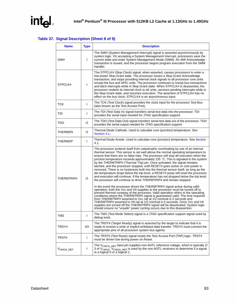
Intel® Pentium® III Processor with 512KB L2 Cache at 1.13GHz to 1.40GHz
SMI# I
The SMI# (System Management Interrupt) signal is asserted asynchronously by system logic. On accepting a System Management Interrupt, processors save the current state and enter System Management Mode (SMM). An SMI Acknowledge transaction is issued, and the processor begins program execution from the SMM handler.
STPCLK# I
The STPCLK# (Stop Clock) signal, when asserted, causes processors to enter a low power Stop-Grant state. The processor issues a Stop-Grant Acknowledge transaction, and stops providing internal clock signals to all processor core units except the bus and APIC units. The processor continues to snoop bus transactions and latch interrupts while in Stop-Grant state. When STPCLK# is deasserted, the processor restarts its internal clock to all units, services pending interrupts while in the Stop-Grant state, and resumes execution. The assertion of STPCLK# has no effect on the bus clock; STPCLK# is an asynchronous input.
TCK I The TCK (Test Clock) signal provides the clock input for the processor Test Bus (also known as the Test Access Port).
TDI I The TDI (Test Data In) signal transfers serial test data into the processor. TDI provides the serial input needed for JTAG specification support.
TDO O The TDO (Test Data Out) signal transfers serial test data out of the processor. TDO provides the serial output needed for JTAG specification support.
THERMDN O Thermal Diode Cathode. Used to calculate core (junction) temperature. See Section 4.1.
THERMDP I Thermal Diode Anode. Used to calculate core (junction) temperature. See Section 4.1.
THERMTRIP# O
The processor protects itself from catastrophic overheating by use of an internal thermal sensor. This sensor is set well above the normal operating temperature to ensure that there are no false trips. The processor will stop all execution when the junction temperature exceeds approximately 135 °C. This is signaled to the system by the THERMTRIP# (Thermal Trip) pin. Once activated, the signal remains latched, and the processor stopped, until RESET# goes active or core power is removed. There is no hysteresis built into the thermal sensor itself; as long as the die temperature drops below the trip level, a RESET# pulse will reset the processor and execution will continue. If the temperature has not dropped below the trip level, the processor will continue to drive THERMTRIP# and remain stopped.
In the event the processor drives the THERMTRIP# signal active during valid operation, both the Vcc and Vtt supplies to the processor must be turned off to prevent thermal runaway of the processor. Valid operation refers to the operating conditions where the THERMTRIP# signal is guaranteed valid. The time required from THERMTRIP# asserted to Vcc rail at 1/2 nominal is 5 seconds and THERMTRIP# asserted to Vtt rail at 1/2 nominal is 5 seconds. Once Vcc and Vtt supplies are turned off the THERMTRIP# signal will be deactivated. System logic should ensure no “unsafe” power cycling occurs due to this deassertion.
TMS I The TMS (Test Mode Select) signal is a JTAG specification support signal used by debug tools.
TRDY# I/OThe TRDY# (Target Ready) signal is asserted by the target to indicate that it is ready to receive a write or implicit writeback data transfer. TRDY# must connect the appropriate pins of all processor system bus agents.
TRST# I The TRST# (Test Reset) signal resets the Test Access Port (TAP) logic. TRST# must be driven low during power on Reset.
VCMOS_REF IThe VCMOS_REF input pin supplies non-AGTL reference voltage, which is typically 2/3 of VCMOS. VCMOS_REF is used by the non-AGTL receivers to determine if a signal is a logical 0 or a logical 1.
Table 37. Signal Description (Sheet 8 of 9)
Name Type Description
Datasheet 83
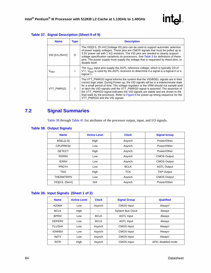
Intel® Pentium® III Processor with 512KB L2 Cache at 1.13GHz to 1.40GHz
7.2 Signal Summaries
Table 38 through Table 41 list attributes of the processor output, input, and I/O signals.
VID [3:0,25mV] O
The VID[3:0, 25 mV] (Voltage ID) pins can be used to support automatic selection of power supply voltages. These pins are CMOS signals that must be pulled up to 3.3V power rail with 1 KΩ resistors. The VID pins are needed to cleanly support voltage specification variations on processors. See Table 3 for definitions of these pins. The power supply must supply the voltage that is requested by these pins, or disable itself.
VREF IThe VREF input pins supply the AGTL reference voltage, which is typically 2/3 of VTT. VREF is used by the AGTL receivers to determine if a signal is a logical 0 or a logical 1.
VTT_PWRGD I
The VTT_PWRGD signal informs the system that the VID/BSEL signals are in their correct logic state. During Power-up, the VID signals will be in a indeterminate state for a small period of time. The voltage regulator or the VRM should not sample and/or latch the VID signals until the VTT_PWRGD signal is asserted. The assertion of the VTT_PWRGD signal indicates the VID signals are stable and are driven to the final state by the processor. Refer to Figure 6 for power-up timing sequence for the VTT_PWRGD and the VID signals
Table 37. Signal Description (Sheet 9 of 9)
Name Type Description
Table 38. Output Signals
Name Active Level Clock Signal Group
BSEL[1:0] High Asynch Power/Other
CPUPRES# Low Asynch Power/Other
DETECT High Asynch Power/Other
FERR# Low Asynch CMOS Output
IERR# Low Asynch CMOS Output
PRDY# Low BCLK AGTL Output
TDO High TCK TAP Output
THERMTRIP# Low Asynch CMOS Output
VID[3:0, 25mV] N/A Asynch Power/Other
Table 39. Input Signals (Sheet 1 of 2)
Name Active Level Clock Signal Group Qualified
A20M# Low Asynch CMOS Input Always1
BCLK High — System Bus Clock Always
BPRI# Low BCLK AGTL Input Always
DEFER# Low BCLK AGTL Input Always
FLUSH# Low Asynch CMOS Input Always1
IGNNE# Low Asynch CMOS Input Always1
INIT# Low Asynch CMOS Input Always1
INTR High Asynch CMOS Input APIC disabled mode
84 Datasheet
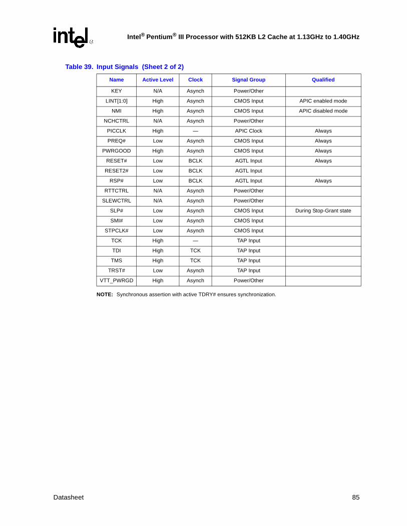
Intel® Pentium® III Processor with 512KB L2 Cache at 1.13GHz to 1.40GHz
NOTE: Synchronous assertion with active TDRY# ensures synchronization.
KEY N/A Asynch Power/Other
LINT[1:0] High Asynch CMOS Input APIC enabled mode
NMI High Asynch CMOS Input APIC disabled mode
NCHCTRL N/A Asynch Power/Other
PICCLK High — APIC Clock Always
PREQ# Low Asynch CMOS Input Always
PWRGOOD High Asynch CMOS Input Always
RESET# Low BCLK AGTL Input Always
RESET2# Low BCLK AGTL Input
RSP# Low BCLK AGTL Input Always
RTTCTRL N/A Asynch Power/Other
SLEWCTRL N/A Asynch Power/Other
SLP# Low Asynch CMOS Input During Stop-Grant state
SMI# Low Asynch CMOS Input
STPCLK# Low Asynch CMOS Input
TCK High — TAP Input
TDI High TCK TAP Input
TMS High TCK TAP Input
TRST# Low Asynch TAP Input
VTT_PWRGD High Asynch Power/Other
Table 39. Input Signals (Sheet 2 of 2)
Name Active Level Clock Signal Group Qualified
Datasheet 85
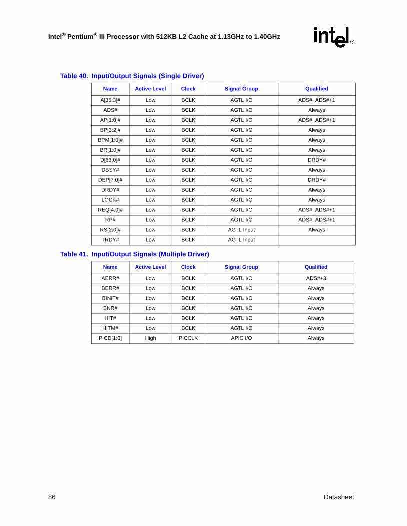
Intel® Pentium® III Processor with 512KB L2 Cache at 1.13GHz to 1.40GHz
Table 40. Input/Output Signals (Single Driver)
Name Active Level Clock Signal Group Qualified
A[35:3]# Low BCLK AGTL I/O ADS#, ADS#+1
ADS# Low BCLK AGTL I/O Always
AP[1:0]# Low BCLK AGTL I/O ADS#, ADS#+1
BP[3:2]# Low BCLK AGTL I/O Always
BPM[1:0]# Low BCLK AGTL I/O Always
BR[1:0]# Low BCLK AGTL I/O Always
D[63:0]# Low BCLK AGTL I/O DRDY#
DBSY# Low BCLK AGTL I/O Always
DEP[7:0]# Low BCLK AGTL I/O DRDY#
DRDY# Low BCLK AGTL I/O Always
LOCK# Low BCLK AGTL I/O Always
REQ[4:0]# Low BCLK AGTL I/O ADS#, ADS#+1
RP# Low BCLK AGTL I/O ADS#, ADS#+1
RS[2:0]# Low BCLK AGTL Input Always
TRDY# Low BCLK AGTL Input
Table 41. Input/Output Signals (Multiple Driver)
Name Active Level Clock Signal Group Qualified
AERR# Low BCLK AGTL I/O ADS#+3
BERR# Low BCLK AGTL I/O Always
BINIT# Low BCLK AGTL I/O Always
BNR# Low BCLK AGTL I/O Always
HIT# Low BCLK AGTL I/O Always
HITM# Low BCLK AGTL I/O Always
PICD[1:0] High PICCLK APIC I/O Always
86 Datasheet