Embed Size (px)
Citation preview

Microwave Transceiver Circuit Building Blocks
by
Eddie Lok Chuen Ng
Engineering-Electrical Engineering and Computer Sciences
in the
GRADUATE DIVISION
of the
UNIVERSITY OF CALIFORNIA, BERKELEY

1
Table of Content Acknowledgments ..................................................................................................................... 2 Chapter 1: Introduction ........................................................................................................... 3
Chapter 2: Low Noise Amplifier Fundamentals
2.1 Introduction....................................................................................................................... 7 2.2 The Role of LNA .............................................................................................................. 8 2.3 LNA Power Gain Definition ........................................................................................... 16 2.4 LNA Stability .................................................................................................................. 18 References................................................................................................................................. 23 Chapter 3: Low Noise Amplifier Topologies 3.1 Introduction..................................................................................................................... 24 3.2 Single Transistor Topologies .......................................................................................... 24 3.3 Noise Match Topologies ................................................................................................. 27 3.4 Power Match Topologies ................................................................................................ 32 3.5 Inductive Degeneration Topologies ................................................................................ 35 3.6 Differential LNA............................................................................................................. 37 References................................................................................................................................. 39 Chapter 4: Low Noise Amplifier Design 4.1 Introduction..................................................................................................................... 40 4.2 LNA Topology Selection ................................................................................................ 40 4.3 Inductive Degenerated LNA Input Network................................................................... 44 4.4 Multi-stage LNA Topology............................................................................................. 47 4.5 Passive Design ................................................................................................................ 51 4.6 LNA Simulation Performance......................................................................................... 54 References................................................................................................................................. 57 Chapter 5: Microwave Frequency Dividers 5.1 Introduction..................................................................................................................... 58 5.2 Frequency Synthesizers................................................................................................... 59 5.3 Wideband Frequency Dividers........................................................................................ 64 5.4 Measurement Results of Wideband Frequency Dividers ................................................ 69 References................................................................................................................................. 72 Chapter 6: Injection-Locked Frequency Dividers 6.1 Introduction..................................................................................................................... 73 6.2 Regenerative Divider ...................................................................................................... 73 6.3 Theory of Injection Locking ........................................................................................... 76 6.4 Introduction of Injection Locked Frequency Divider ..................................................... 78 6.5 Design of Oscillator in ILFD .......................................................................................... 79 6.6 Design of Transconductor in ILFD................................................................................. 87 6.7 Measurement Results of ILFD........................................................................................ 91 6.8 CMOS Injection-locaked Frequency Divider ................................................................. 94 References................................................................................................................................. 95 Chapter 7: Conclusions .......................................................................................................... 96

2
Acknowledgments
This project is made possible by my advisor and many other facilities in the EECS
department. They make a very challenging project available and I am very fortunate to be
a part of it. This work would not be possible without the guidance of them.
My colleagues here at Berkeley: Hanching Fuh, Mounir Bohsali, Axel Berny, Jon
Choy, Mark Chew, Richard Lu, Nathan Chan, Ada Poon, Ken Oo, Janie Zhou, Bill
Tsang, Chee Yuen Hui, all the 60GHz members and many others make graduate life
easier. They share all the joy and suffering together with me over the last couple years. I
am so glad to work with such talented and interesting group of people. I really appreciate
the support and help that they offer. I really want to thank all my professors from my
undergradutae study. They gave me a strong foundation in engineering while keeping the
subject interesting. A special thank you to my best friends in Hong Kong: Eric Li, Derek
Li, Ricky Wong and Dominic Yu. I had the most wonderful time when we were
together.
I would like to thank my parents for their unconditional support. They provide all
the motivation that I need in school and in life. A simple thank you is never enough and
there are no words to describe the love and care that they give me. Also I would like to
thank my sisters for their company and understanding as well.
3
Chapter 1
Introduction
With the advancement of commercial CMOS and bipolar technologies, fT and fmax
of the transistors are well above 100GHz. However, most circuit designs in such
processes only operate up to about 10GHz or fT/10. The 60GHz wireless local area
network project explores the possibility of RF/microwave designs at fT/2, utilizing these
very same low-cost commercial processes.
As shown in Figure 1-1 [1], due to oxygen absorption there will be high channel
attenuation at 60GHz, making long distance communication impractical. As a result, the
60GHz system is targeted for indoor application at this vacant frequency band.
However as the carrier frequency gets higher, the corresponding wavelength gets
shorter. The effective area of the antenna is also smaller, decreasing the received power.
To combat this problem, a multi-antenna WLAN system is employed, as shown in Figure
1-2. Utilizing directional beam forming, this architecture improves antenna gain
significantly, but at the expense of power dissipation due to multiple receiver paths.
Consequently, power dissipation of individual blocks of each receive/transmit chain must
be low while providing adequate performance at the carrier frequency.

4
Figure 1-1 Attenuation vs Frequency in free space [1]
At the circuit level, many challenges arise at such high frequency. As fo/fT
approaching unity, typical performance such as high gain, low power and low noise
become a challenging task to achieve. As a result, the most important goal is to design
transceiver building blocks that could operate up to the carrier frequency.
Good quality passives are essential but difficult to realize because of the
proximity of the lossy substrate. As the passives physical dimensions approach fractions
of the wavelength, distributed effects start to take over and traditional lumped models
begin to fail. As a result, testing and characterization of both actives and passives are a
big part of the overall project.
100
10 20 40 70 100 200 400 700 1000 0.01 0.02 0.05
0.1 0.2 0.5
1 2 5
10 20 50
Frequency - f (GHz)
Attenuation - γ (dB/km)
Oxygen absorption

5
The focus of this work is to explore the design methodology of a fully integrated
microwave low power and high gain low noise amplifier targeted at 30GHz, as discussed
in chapters 2 and 3. In chapter 4, a prototype 30GHz SiGe LNA is investigated and
implemented which dissipates only 22mW and provides |S21|>20dB.
Figure 1-2 Block Diagram of 60GHz WLAN
Figure 1-3 Typical Wireless Transceiver Block
VCO
Filter IF Amp A/D
VCO
Filter IF Amp A/D
VCO
Filter IF Amp A/D
LNA
LNA
LNA
Path 1
Path 2
Path N. . .
. . .
. . .
. . .
LNA Filter ADC IF AMP
DAC
Duplexer
PA Filter
IF AMP Freq Syn.

6
As a second part, different frequency dividers are investigated as part of the
frequency synthesizer which is an essential component in a frequency modulated wireless
system (see Figure 1-3).
Within the synthesizer, the VCO and the divider both operate at the local
oscillator frequency which is the highest frequency in the synthesizer loop. Therefore
both could dissipate power a few order magnitude higher than other blocks (see Figure 1-
4). Since the divider is one of the major power consumption blocks, the conventional
wideband static latch-based divider is first discussed in chapter 5.
In chapter 6, an analog-based divider is introduced. This narrow-band injection-
locked divider is explored and verified as a low-power high-frequency alternative divider
for the 60GHz WLAN project.
Figure 1-4 Typical Frequency Synthesizer Loop
Reference
[1] Vilhelm Gregers-Hansen, Radio Propagation at 90GHz Slides, Radar Division, Naval Research
Laboratory, Presented at FCC Forum:“New Horizons : 90 GHz Technologies”July 14, 2000
PFD Loop filter VCO
÷N
fref
fLO/N
fLO Vcontrol

7
Chapter 2
Low Noise Amplifier Fundamentals
2.1 Introduction
In a wireless transceiver, the low noise amplifier (LNA) is a critical
building block in the receiver path. Typical receiver architecture is shown in Figure 2-1.
The antenna receives electromagnetic waves from free space and converts them into
waves in transmission lines. Even though the antenna has its own frequency response,
most systems provide further filtering with a RF filter (not shown in Figure 2-1). This
potentially weak received signal is directly fed to the first stage, the LNA, which provides
adequate gain without degrading the signal significantly, to alleviate the signal to noise
ratio (SNR) of subsequent stages. The mixer and the VCO translate the signal from the
carrier frequency to some intermediate frequency, which is further processed by the
baseband circuitry. In this chapter, general roles LNA are investigated. Different LNA
design parameters are also discussed.
Figure 2-1 Typical Wireless Receiver System
VCO
IF Amp A/D LNA
Filter

8
2.2 The Role of LNA
As discussed, the LNA is the first gain stage in the receiver path. There are many
important tasks that the LNA must be able to handle. As its name suggested, the LNA has
to provide low noise amplification. The overall noise performance of the receiver is set
by the LNA, whose noise figure (NF) directly adds to the system’s NF. Noise figure is
defined as the ratio of the input SNR to the output SNR,
o
i
SNRSNR
NF = (1)
and is a direct measure of how much a system degrades the signal. In a noiseless system,
for instance, a wire with zero length, SNRi=SNRo, giving NF=1 or 0dB. This ideal
system never exists and in reality, the NF is always greater than 1 or 0dB.
In a cascaded system, there are many blocks providing various tasks such as
amplification, frequency modulation and filtering etc. As shown in Figure 2-2, each
individual block can be characterized with its NF and available power gain, Ap. The
overall noise figure of such system can be calculated [1] as
)1(121
3
1
21 ...
1...
11
−
−+
−+
−+=
Npp
N
ppptot AA
NFAA
NFA
NFNFNF (2)
Figure 2-2 Typical Cascade System Block Diagram
NF1,Ap1 NF2,Ap2 NFN,ApN
Stage 1 Stage 2 Stage N

9
Equation (2) shows that the first stage’s NF directly affects the overall NF. The
cascaded gain reduces NF contribution of subsequent stages, adding negligible effect on
the overall NF. This sets the overall sensitivity of the receiver path since the noise
performance determines the lower limit of received signal that can be detected.
Besides the noise performance, the LNA also has to provide adequate gain at RF,
even though most gain stages are located at IF or baseband since at the intermediate
frequency, higher gain is easier to obtain at lower power. As equation (2) suggests, the
gain of the first stage appears in the denominator of every term. The higher the first stage
gain is, the less effect subsequent stages will have on the NF. Unlike equation (1), the
simple NF equation, equation (3) is the NF of an infinite cascade of identical stages
which takes into consideration of gain. As see from the equation, NF∞ approaches the NF
of one stage as the power gain goes to infinity.
1,11
1
>−
−=∞ A
A
ANF
NF (3)
This explains the importance of having adequate gain at the carrier frequency. Moreover
the LNA gain must not be too high to cause overloading in the mixer stage or subsequent
stages.
Figure 2-3 LNA input impedance in the RX path with RF filter
VCO
FilterFilter LNA

10
The LNA also has an important task of providing impedance matching to the
filters or antenna. As seen in Figure 2-3, an RF filter is sometimes inserted between the
antenna and the LNA to further notch out interferers. Even though a RF filter may not be
used in some systems, like the 60GHz WLAN, the LNA still has to provide proper
termination such that the antenna can operate with the desired frequency response.
A typical impedance value of 50-Ω is chosen for most systems as a compromise
between the 30-Ω resistance for maximum power handling and the 77-Ω resistance for
minimum loss [2]. Most microwave and surface acoustic wave (SAW) filters require this
50-Ω termination to achieve the attenuation and cutoff frequency as a required parameter.
In addition, by providing impedance matching the LNA will also benefit from
maximum power transfer. Figure 2-4 is a simple amplifier circuit. The power transfer to
the load is [3]
222
)()(||
21
gingin
ing XXRR
RVP
+++= (4)
gggininin jXRZandjXRZwhere +=+=
If Zin is the complex conjugate of Zg then maximum power transfer occurs which equals
gg R
VP4
1||21 2
max = (5)

11
Figure 2-4 Simple Amplifier circuit
Selecting the antenna/filter and LNA input/output impedances as real 50-Ω
resistance achieves conjugate matching and maximum power transfer at the same time.
The LNA in addition provides reverse isolation for the antenna. As shown in
Figure 2-5, the large LO signal generated from the VCO will leak through the mixer and
the LNA, finding its way back to the antenna. If the reverse isolation of the LNA is not
sufficient, a large LO signal may appear at the antenna, which will convert this LO signal
into EM wave and contaminate the RF spectrum. This could lead to inter-modulation and
self-mixing, creating DC offset in the baseband. This situation is extremely troublesome
in a direct-conversion system where the IF is at DC.
Figure 2-5 LO leakage problem in the RX path
LNA
Zg
Vg
Zin
ZL
Zout
LO leakage
LNA
LO radiating

12
Finally the LNA sets the upper limit of acceptable received input signal as well.
We have seen the LNA sets the lower limit of the received input signal due to the finite
NF. The upper limit is set by the LNA’s distortion, which causes gain compression and
undesired frequency tones in the signal path. Ideally the LNA would see one tone at the
carrier frequency. However interferers always exist, creating inter-modulation.
Considering a single interferer centered at ω2 as in the Figure 2-6. The input to the LNA
can be expressed as
tStSSi 2211 coscos ωω += (6)
The LNA produces an output signal, which can be expressed as a Taylor series as:
....33
221 iiio SaSaSaS ++= (7)
Figure 2-6 Typical Received Spectrum
ω
SRX(f)
ω 1 ω2

13
Substituting equation (6) into (7) and letting S1=S2 for testing purposes, the inter-
modulation term IM3 is found as [4]:
21
1
33 4
3 Saa
IM = (8)
IM3 is very important in receiver and LNA design when ω1 ~ ω2, because the tones at
2*ω2-ω1 and 2*ω1-ω2 fall back to the input spectrum and cannot be easily filtered out (see
Figure 2-7).
The input intercept point IIP3 is defined when IM3 is set to 1 and from equation (8)
3
13 3
4aa
SIIP i == (9)
Figure 2-7 RX Output Spectrum
ω
So(f)
ω 1 ω2
Filter Response
2ω 1- ω 2 2ω 2- ω 1
ω 1- ω 2
14
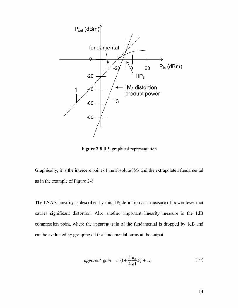
Figure 2-8 IIP3 graphical representation
Graphically, it is the intercept point of the absolute IM3 and the extrapolated fundamental
as in the example of Figure 2-8
The LNA’s linearity is described by this IIP3 definition as a measure of power level that
causes significant distortion. Also another important linearity measure is the 1dB
compression point, where the apparent gain of the fundamental is dropped by 1dB and
can be evaluated by grouping all the fundamental terms at the output
...)14
31( 331 ++= iS
aa
againapparent (10)
0
-20
-40
-60
-20 0 20
IM3 distortion product power
fundamental
Pin (dBm)
Pout (dBm)
-80
1
3
IIP3
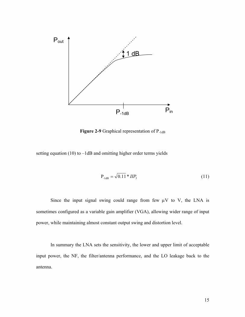
15
Figure 2-9 Graphical representation of P-1dB
setting equation (10) to –1dB and omitting higher order terms yields
31dB- *11.0P IIP= (11)
Since the input signal swing could range from few µV to V, the LNA is
sometimes configured as a variable gain amplifier (VGA), allowing wider range of input
power, while maintaining almost constant output swing and distortion level.
In summary the LNA sets the sensitivity, the lower and upper limit of acceptable
input power, the NF, the filter/antenna performance, and the LO leakage back to the
antenna.
1 dB
P-1dB Pin
Pout

16
2.3 LNA Power Gain Definition
The power gain expressions of the LNA can be described using the input and
output reflection coefficients defined as
oL
oLL ZZ
ZZ+−
=Γ (12)
og
ogg ZZ
ZZ+
−=Γ (13)
The average power delivered to the network is [3]
)||1(|1|
|1|8
|| 22
22
ining
g
o
gin Z
VP Γ−
ΓΓ−
Γ−= (14)
while the power delivered to the load is
2222
22221
2
|1||1||1|)||1(||
8||
ingL
gL
o
gL S
SZ
VP
ΓΓ−Γ−
Γ−Γ−= (15)
Figure 2-10 A LNA connected with general source and load impedances.
[S]
Zg
Vg
Zin
ZL
Zout

17
Taking the ratio of equations (14) and (15) gives the power gain
)||1(|1|)||1(||
2222
2221
inL
L
in
L
SS
PP
Γ−Γ−Γ−
= (16)
Note that when Γin=ΓL=0, the power gain is equal to |S21|2. This is the case when the
source and load impedances are both matched to 50Ω.
Other definitions of power gain are also defined in [3] such as available power gain
)||1(|1|)||1(||
2211
2221
outg
gA S
SG
Γ−Γ−
Γ−= (17)
which is the ratio of power available from the network to power available from the source
and transducer power gain
222
2
22221
|1||1|)||1()||1(||
Ling
LgT S
SG
Γ−ΓΓ−
Γ−Γ−= (18)
which is the ratio of power to the load to power available from the source. A special case
occurs when S12=0 and the unilateral gain can be defined
222
211
22221
|1||1|)||1()||1(||
Lg
LgTU SS
SG
Γ−Γ−
Γ−Γ−= (19)
All the above expressions simplify to |S21|2 when input and output impedances are
matched to the source and load impedances respectively.
18
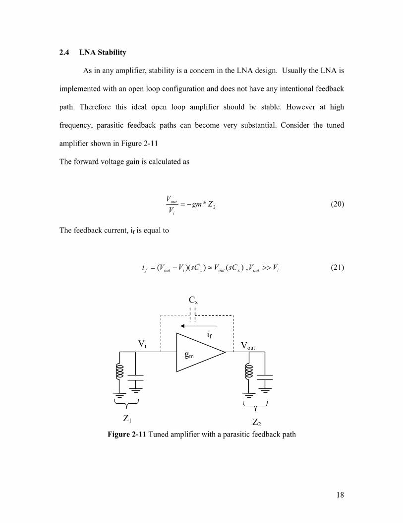
2.4 LNA Stability
As in any amplifier, stability is a concern in the LNA design. Usually the LNA is
implemented with an open loop configuration and does not have any intentional feedback
path. Therefore this ideal open loop amplifier should be stable. However at high
frequency, parasitic feedback paths can become very substantial. Consider the tuned
amplifier shown in Figure 2-11
The forward voltage gain is calculated as
2* ZgmV
V
i
out −= (20)
The feedback current, if is equal to
ioutxoutxioutf VVsCVsCVVi >>≈−= ,)())(( (21)
Figure 2-11 Tuned amplifier with a parasitic feedback path
gm
Vi Vout
Cx
Z2Z1
if
19
and the reverse gain is
))(( 11 outxfi VZsCZiV ==
1ZsCVV
xout
i = (22)
Combining equations (20) and (22), yields the loop gain
xl sCZgmZA 21−= (23)
The forward voltage gain contributes 180o from the phase inversion; the capacitive
feedback contributes 90o and therefore if there is a 90o more phase shift introduced by the
input and output tanks, oscillation could occur when the loop gain is greater than unity.
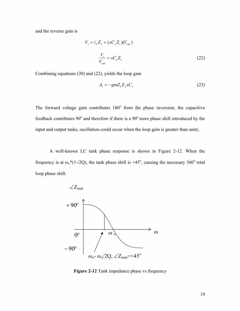
A well-known LC tank phase response is shown in Figure 2-12. When the
frequency is at ωo*(1-/2Q), the tank phase shift is +45o, causing the necessary 360o total
loop phase shift.
Figure 2-12 Tank impedance phase vs frequency
°+90
°−90
°0
∠Ztank
ω o
ωo- ωo/2Q, ∠Ztank=+45o
ω
20
As a result from equation (23) oscillation occurs when [4]
122
|||| 2121 >== xxl C
RRgmsCZgmZA ω (24)
To avoid the possible oscillation, equation (24) suggests that parasitic capacitor Cx or the
feedback effect should be kept small.
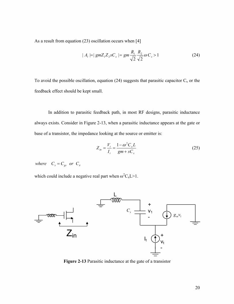
In addition to parasitic feedback path, in most RF designs, parasitic inductance
always exists. Consider in Figure 2-13, when a parasitic inductance appears at the gate or
base of a transistor, the impedance looking at the source or emitter is:
x
x
t
tin sCgm
LCIV
Z+
−==
21 ω (25)
πCorCCwhere gsx =
which could include a negative real part when ω2CxL>1.
Figure 2-13 Parasitic inductance at the gate of a transistor
1vgm
L
+ v1-
xC
+vt-
ItZin
21
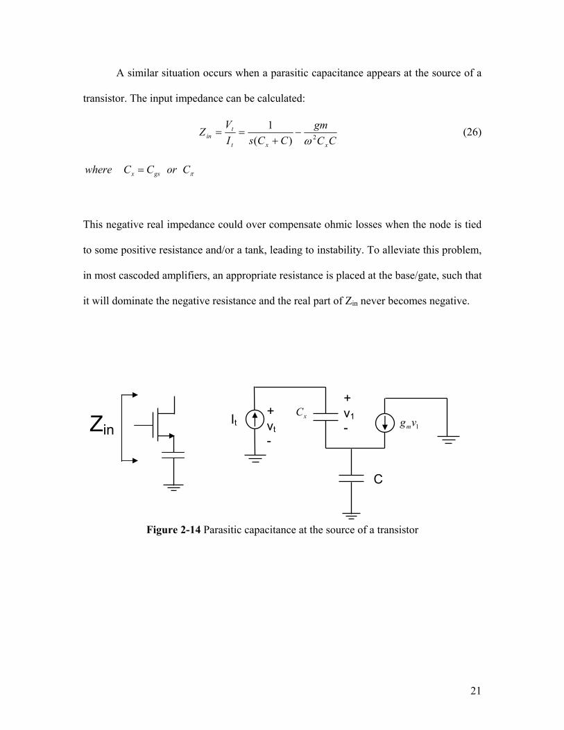
A similar situation occurs when a parasitic capacitance appears at the source of a
transistor. The input impedance can be calculated:
CCgm
CCsIV
Zxxt
tin 2)(
1ω
−+
== (26)
πCorCCwhere gsx =
This negative real impedance could over compensate ohmic losses when the node is tied
to some positive resistance and/or a tank, leading to instability. To alleviate this problem,
in most cascoded amplifiers, an appropriate resistance is placed at the base/gate, such that
it will dominate the negative resistance and the real part of Zin never becomes negative.
Figure 2-14 Parasitic capacitance at the source of a transistor
1vgm
C
+v1-
xC+vt-
ItZin

22
As we can see, oscillation is possible if either the input or output port impedance
has a negative real part; this would imply that either the input or output reflection
coefficient is greater than one, |Γin|>1 or |Γout|>1 [3].
Using S parameters matrix, we can determine if a circuit, like the LNA, is stable
or not. The Stern stability factor is calculated [3] as
||*||2||||||1
1221
222
211
2
SSSSK −−∆+
= (27)
21122211 SSSS −=∆
if K>1 and |∆|<1, the circuit is unconditionally stable under any combination of source
and load impedances. This stability factor is a pessimistic measure of the LNA’s stability
since source and load impedances are usually known and do not vary much. In fact, a
circuit could be stable without satisfying this condition.
As seen from equation (27), when S12 is decreased, the circuit becomes more
stable. This agrees with the earlier statement that improving reverse isolation of the LNA
is the key to improve stability.

23
References
[1] Behzad Razavi, RF Microelectronics, Prentice Hall PTR; 1st edition
[2] Dennis Yee, A Design Methodology for highly-Integrated Low-Power Receivers for Wireless
Communications, UC Berkeley PhD Dissertation
[3] David Pozar, Microwave Engineering, John Wiley & Sons; 2nd Edition
[4] Robert Meyer, EE242 Lecture Notes
[5] Guillermo Gonzalez, Microwave Transistor Amplifiers Analysis and Design, Prentice Hall PTR; 2nd
edition
[6] Thomas Lee, The Design of CMOs Radio Frequency Integrated Circuits, Cambridge Univ Pr
[7] D.K. Shaeffer and T.H. Lee, “A 1.5V, 1.5GHz CMOS Low Noise Amplifier,” IEEE Journal of Solid-
State Circuits, VOL. 32, No.5 May 1997
[8] Paul Gray and Robert Meyer, Analysis and Design of Analog Integrated Circuits, John Wiley & Sons;
3rd edition
[9] C.Y. Wu, S.y Hsiao, The Design of a 3V 900MHz CMOS Bandpass Ampilifer, IEEE Journal of Solid-
State Circuits, VOL. 32, NO. 2, FEBRUARY 1997
[10] R. Rafla and M.El-Gamal, “Design of a 1.5V CMOS Integrated 3GHz LNA,” ISCAS 99, Vol. II, pp.
440-443, June 1999
[11] Xi Li, T. Brogan, M. Esposito, B.Meyers and Kenneth K.O, “A Comparison of CMOS and SiGe
LNA’s and Mixers for Wireless LNA Application,” Custom Integrated Circuits, 2001, IEEE Conference
on. , 6-9 May 2001
[12] Yongwang Ding, Ramesh Harjani, “A +18dBm IIP3 LNA in a 0.35um CMOS,” Solid-State Circuits
Conference, 2001
[13] R.C Liu, C.R Lee, H. Wanf and C.K. Wang, “A 5.8GHz Two-Stage High-Linearity Low Voltage low
Noise amplifier in a 0.35um CMOS Technology,” 2002 IEEE RFIC Symposium
[14] Xiaomin Yang, Thomas Wu and John McMacken, Design of LNA at 2.4GHz Using 0.25um
Technology, Silicon Monolithic Integrated Circuits in RF Systems, 2001
[15] C. Tinella, J.M Founier, J. Haidar, “Noise Contribution in a Fully Integrated 1V 2.5GHz LNA in
CMOS-SOI Technology,” Electronics, Circuits and Systems, 2001. ICECS 2001.

24
Chapter 3
Low Noise Amplifier Topologies
3.1 Introduction
As seen from the previous chapter, there are many tasks that a LNA must be able
to perform. As a result, many different topologies are put together to satisfy a particular
performance need. More specifically, there are two major categories that a LNA fall
into—noise or power matched. Circuit examples of each will be explored. Noise figure
comparison of each topology is calculated as a measure of the LNA’s performance.
Simple one transistor amplifier topologies are first investigated, and then other design
techniques are explored later in the chapter.
3.2 Single Transistor Topologies
After exploring the LNA’s tasks and parameters, we will look at some circuit
implementations and their performance. In order to obtain low NF, we identify that the
important design consideration is to minimize the use of noisy elements such as resistors
and/or transistors. We will first start considering the one-transistor amplifier topologies,
namely the common collector/drain, common base/gate, and the common emitter/source.
The common collector/drain provides less than unity voltage gain and has low
output impedance. As we have seen previously, the LNA should provide sufficient power

25
gain to lessen the noise contribution of subsequent stages. Although common
collector/drain configuration can achieve this power gain requirement, the drawback is
that the input voltage must be able to swing very high, in fact higher than the output
swing. This voltage following property is troublesome, since when the received signal is
weak, the baseband A/D converters will not be able to process such small voltage swing.
As a result, the common collector/drain configuration is not a good choice for the LNA.
The AC equivalent of common base and gate amplifiers are shown in Figure 3-1.
The input impedances of both common base and gate must be chosen such that they
match to the source resistance of 50Ω. This results in a major drawback that the
transconductance, gm, of the transistor is fixed. The gain of the matched condition,
gm*|ZL|=|ZL|/RS, is also predetermined.
Figure 3-1 Common base and common gate amplifiers.
mg1
SR
ZL
mbm gg +1
SR
ZL
26
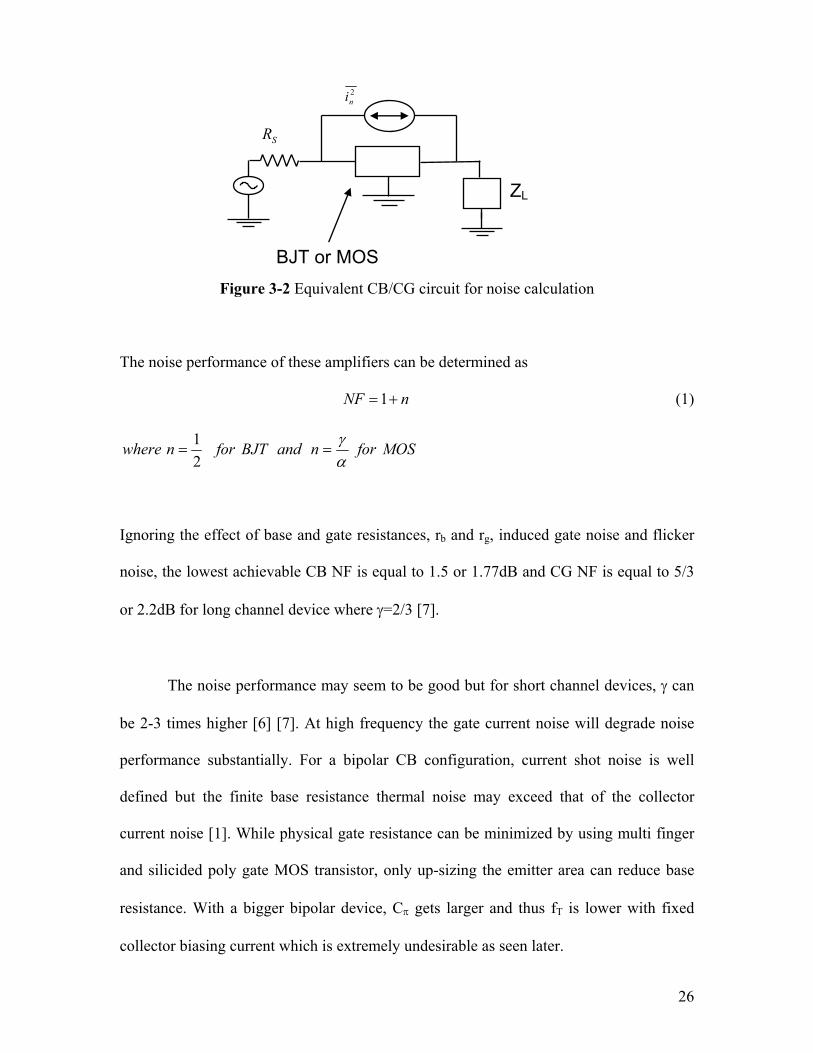
Figure 3-2 Equivalent CB/CG circuit for noise calculation
The noise performance of these amplifiers can be determined as
nNF +=1 (1)
MOSfornandBJTfornwhereαγ
==21
Ignoring the effect of base and gate resistances, rb and rg, induced gate noise and flicker
noise, the lowest achievable CB NF is equal to 1.5 or 1.77dB and CG NF is equal to 5/3
or 2.2dB for long channel device where γ=2/3 [7].
The noise performance may seem to be good but for short channel devices, γ can
be 2-3 times higher [6] [7]. At high frequency the gate current noise will degrade noise
performance substantially. For a bipolar CB configuration, current shot noise is well
defined but the finite base resistance thermal noise may exceed that of the collector
current noise [1]. While physical gate resistance can be minimized by using multi finger
and silicided poly gate MOS transistor, only up-sizing the emitter area can reduce base
resistance. With a bigger bipolar device, Cπ gets larger and thus fT is lower with fixed
collector biasing current which is extremely undesirable as seen later.
SR
2ni
ZL
BJT or MOS

27
3.3 Noise Match Topologies
Figure 3-3 CE and CS LNA implementations
Let’s take a look at the CS and CE configurations (see Figure 3-3). The voltage
gain of these amplifiers is readily calculated as –gmZL which is the same as the CG and
CB configurations. However unlike CB/CG, the transconductance, gm does not affect the
input impedance.
The noise performance of the bipolar CE implementation can be calculated using
Figure 3-4 and defining the noise sources [8]
RL CL LRL CLL
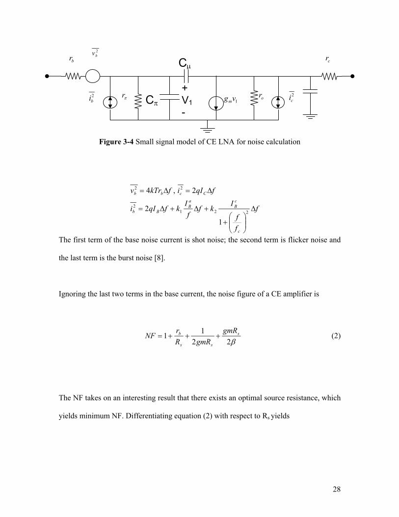
28
Figure 3-4 Small signal model of CE LNA for noise calculation
The first term of the base noise current is shot noise; the second term is flicker noise and
the last term is the burst noise [8].
Ignoring the last two terms in the base current, the noise figure of a CE amplifier is
β2211 s
ss
b gmRgmRR
rNF +++= (2)
The NF takes on an interesting result that there exists an optimal source resistance, which
yields minimum NF. Differentiating equation (2) with respect to Rs yields
f
ff
Ikff
IkfqIi
fqIifkTrv
c
cB
aB
Bb
Ccbb
∆
+
+∆+∆=
∆=∆=
2212
22
1
2
2,4
Cπ
Cµ
2ci2
bi πr+ V1-
1vgmor
br2bv
cr
29
)12(1
02
)2
1()(
,
2
+=
=++−
=
bopts
s
b
s
gmrgm
R
gmR
gmr
dRNFd
β
β
β121min
++= bgmrNF (3)
NF decreases as rb decreases and β increases. gm is chosen for the appropriate gain. At
high frequency:
ωω
ωωβ
ββ T
T
o
o
j→
+=
1 (4)
indicating the higher the unity gain frequency fT is, the lower the noise figure will be.
For the CS MOS amplifier case, we can define the noise sources as [6]
do
gsg
Gggng
aD
dod
gC
g
fqIifgkTi
ff
IkfgkTi
5,
34
2,4
4
22
22
2
ωδ
δ
γ
==
∆=∆=
∆+∆=
30
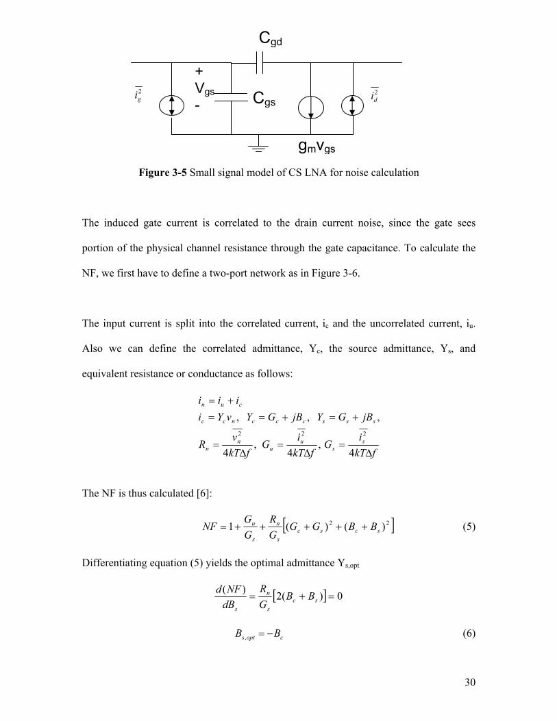
Figure 3-5 Small signal model of CS LNA for noise calculation
The induced gate current is correlated to the drain current noise, since the gate sees
portion of the physical channel resistance through the gate capacitance. To calculate the
NF, we first have to define a two-port network as in Figure 3-6.
The input current is split into the correlated current, ic and the uncorrelated current, iu.
Also we can define the correlated admittance, Yc, the source admittance, Ys, and
equivalent resistance or conductance as follows:
The NF is thus calculated [6]:
[ ]22 )()(1 scscs
n
s
u BBGGGR
GG
NF +++++= (5)
Differentiating equation (5) yields the optimal admittance Ys,opt
[ ] 0)(2)(=+= sc
s
n
s
BBGR
dBNFd
copts BB −=, (6)
Cgs
Cgd
2di
2gi
gmvgs
+ Vgs -
fkTi
GfkT
iG
fkTv
R
jBGYjBGYvYiiii
ss
uu
nn
ssscccncc
cun
∆=
∆=
∆=
+=+==+=
4,
4,
4
,,,222

31
Figure 3-6 Generic two port network used for noise calculation
[ ] [ ] 0)()()(2)( 2222 =+++−++−= scscs
nsc
s
n
s
u
s
BBGGGR
GGGR
GG
dGNFd
optsscn
uopts BBforG
RGG ,
2, =+= (7)
ccn
uopts jBG
RG
Y −+= 2, (8)
For a MOS transistor, the values of Gc, Bc, Rn, and Gu are given in reference [6] and the
optimal source admittance and NF is calculated as:
+−=
γδαω5
||1 cCB gsopt
)||1(5
2cCG gsopt −=γδαω
)||1(5
21 2min cNF
T
−+≈ γδωω (9)
where c is the correlation coefficient between the induced gate and drain current noise.
Noiseless Two-port Network
2ni
2nv

32
Equation (9) reveals that NF is once again inversely proportional to fT, leading to the
conclusion that if one wants to achieve minimum NF, fT must be maximized.
3.4 Power Match Topologies
As we seen from the above analysis, the optimal source impedance is usually
different from the desired 50-Ω termination value. As a result, in most situations
minimum noise figure and maximum power transfer cannot be achieved simultaneously.
In most situations, power match is preferred, even though noise performance is not
optimal. In this section, some impedance matching topologies are explored and tradeoffs
of NF will be discussed.
Shown in Figure 3-7 is a simple power match CS/CE circuit implementation. This
technique of resistive termination is very wideband but as mentioned before, noise is
degraded when resistance is added. Furthermore, the input impedance of the transistor
has a capacitive term which varies with frequency; thus this configuration cannot achieve
optimal S11 performance.
Figure 3-7 CE and CS resistive input termination match circuit
RL CLL
Rp
RS
RL CLL
Rp
RS

33
The NF is calculated to be
2
1
+++=
p
sp
ss
p
RRR
gmRn
RR
NF (10)
MOSfornandBJTfornwhereαγ
==21
If we ignore the noise contribution from the transistor, the minimum NF achievable is
1+Rp/Rs=2 or 3dB. This topology gives very poor minimum NF and the important
concept acquired from this circuit is to design an input match termination without
suffering from the actual 50-Ω resistance thermal noise.
One way to accomplish that is the use of negative feedback, which modifies input
and output impedances by the loop gain. Shown in Figure 3-8 is such a circuit, so called
shunt-series amplifier.
The gain is approximately equal to [6]
11 1
1
>>+
−=−≅ gmRforgmR
gmRRGA LLmV
1R
RA LV −≈ (11)
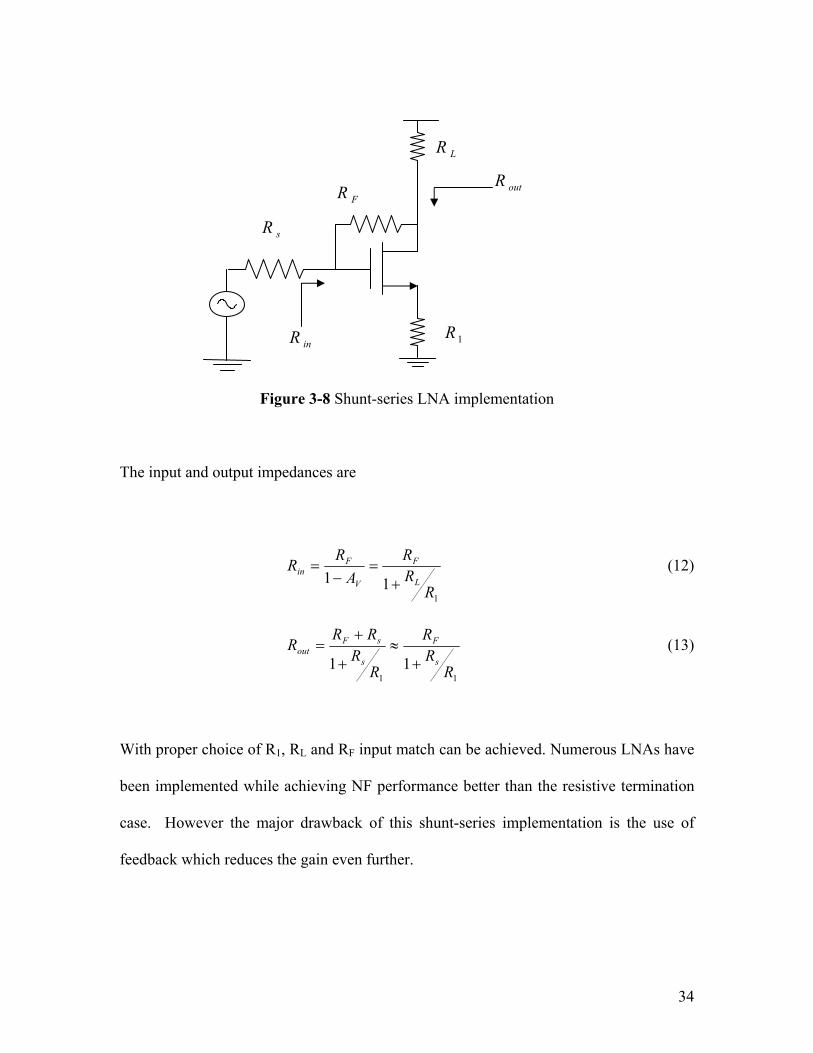
34
Figure 3-8 Shunt-series LNA implementation
The input and output impedances are
111
RRR
AR
RL
F
V
Fin
+=
−= (12)
1111 R
RR
RR
RRR
s
F
s
sFout
+≈
+
+= (13)
With proper choice of R1, RL and RF input match can be achieved. Numerous LNAs have
been implemented while achieving NF performance better than the resistive termination
case. However the major drawback of this shunt-series implementation is the use of
feedback which reduces the gain even further.
1R
sR
LR
FR
inR
outR

35
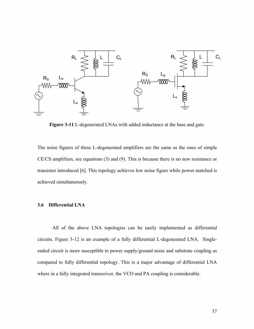
3.5 Inductive Degeneration Topologies
As indicated earlier, the most effective way to minimize noise is to minimize the
use of transistor and resistor. The ideal amplifier would utilize no resistor and still be able
to provide a real 50Ω impedance at the input, achieving impedance/power match to the
antenna and/or filter.
Consider the circuit of Figure 3-9 where an inductor is used as degeneration. If we
ignore the Miller effect and base/gate resistance for the moment, we can calculate the
input impedance as follow:
xxt
tin sC
sLC
gmLiv
Z 1++== (14)
xT C
gmwith =ω
)1(x
Tin CLjLZ
ωωω −+= (15)
Figure 3-9 LNA implement with inductive degeneration
RL CLLL
Le
RS
RL CLLL
Ls
RS
Zin Zin

36
Figure 3-10 Small signal model of L-degenerated amplifier
From equation (15), the input impedance of a L-degenerated CE/CS amplifier has
a real term, ωTL. This real part of the impedance can be used to match to the system
impedance of 50Ω without suffering from the thermal noise of an actual resistor.
Equation (15) reveals that once the transistor is biased, ωT is fixed and the
degeneration inductor, L, can be chosen to provide a real part of 50Ω. Note that one can
purposely introduce extra Cx to adjust ωT to provide a real impedance of 50Ω, but by
doing so, ωT drops which increases NF. Since we desire the imaginary part of the
impedance to be zero, ωL should be set to 1/ωCx . However this is usually not the
situation and thus a base/gate inductor is added to tune out Cx (see Figure 3-11).
The base/gate resistance will add in series to the real part of equation (14). The
effect of Cµ and Cgd is more involved mathematically, but intuitively it adds more
capacitive imaginary part to the input impedance. More in depth design procedures of L-
degenerated LNA are described in the next chapter.
1vgm
L
+ v1-
xC+ vt -
it
37
Figure 3-11 L-degenerated LNAs with added inductance at the base and gate.
The noise figures of these L-degenerated amplifiers are the same as the ones of simple
CE/CS amplifiers, see equations (3) and (9). This is because there is no new resistance or
transistor introduced [6]. This topology achieves low noise figure while power matched is
achieved simultaneously.
3.6 Differential LNA
All of the above LNA topologies can be easily implemented as differential
circuits. Figure 3-12 is an example of a fully differential L-degenerated LNA. Single-
ended circuit is more susceptible to power supply/ground noise and substrate coupling as
compared to fully differential topology. This is a major advantage of differential LNA
where in a fully integrated transceiver, the VCO and PA coupling is considerable.
RL CLL
Le
RS
RL CLL
Ls
RSLb Lg

38
However some antennas are monopole, providing single-ended output.
Converting single-ended signal to differential signal requires a balun, which introduces
insertion loss and extra noise. In addition to that, at this frequency the capacitive coupling
between winding dominates inductive coupling. One must utilize EM field solver to
carefully consider these tradeoffs introduced by the balun.
Figure 3-12 Fully Differential LNA
RL CLL
Le
Lb
RLCL L
Le
Lb

39
References
[1] Behzad Razavi, RF Microelectronics, Prentice Hall PTR; 1st edition
[2] Dennis Yee, A Design Methodology for highly-Integrated Low-Power Receivers for Wireless
Communications, UC Berkeley PhD Dissertation
[3] David Pozar, Microwave Engineering, John Wiley & Sons; 2nd Edition
[4] Robert Meyer, EE242 Lecture Notes
[5] Guillermo Gonzalez, Microwave Transistor Amplifiers Analysis and Design, Prentice Hall PTR; 2nd
edition
[6] Thomas Lee, The Design of CMOs Radio Frequency Integrated Circuits, Cambridge Univ Pr
[7] D.K. Shaeffer and T.H. Lee, “A 1.5V, 1.5GHz CMOS Low Noise Amplifier,” IEEE Journal of Solid-
State Circuits, VOL. 32, No.5 May 1997
[8] Paul Gray and Robert Meyer, Analysis and Design of Analog Integrated Circuits, John Wiley & Sons;
3rd edition
[9] C.Y. Wu, S.y Hsiao, The Design of a 3V 900MHz CMOS Bandpass Ampilifer, IEEE Journal of Solid-
State Circuits, VOL. 32, NO. 2, FEBRUARY 1997
[10] R. Rafla and M.El-Gamal, “Design of a 1.5V CMOS Integrated 3GHz LNA,” ISCAS 99, Vol. II, pp.
440-443, June 1999
[11] Xi Li, T. Brogan, M. Esposito, B.Meyers and Kenneth K.O, “A Comparison of CMOS and SiGe
LNA’s and Mixers for Wireless LNA Application,” Custom Integrated Circuits, 2001, IEEE Conference
on. , 6-9 May 2001
[12] Yongwang Ding, Ramesh Harjani, “A +18dBm IIP3 LNA in a 0.35um CMOS,” Solid-State Circuits
Conference, 2001
[13] R.C Liu, C.R Lee, H. Wanf and C.K. Wang, “A 5.8GHz Two-Stage High-Linearity Low Voltage low
Noise amplifier in a 0.35um CMOS Technology,” 2002 IEEE RFIC Symposium
[14] Xiaomin Yang, Thomas Wu and John McMacken, Design of LNA at 2.4GHz Using 0.25um
Technology, Silicon Monolithic Integrated Circuits in RF Systems, 2001
[15] C. Tinella, J.M Founier, J. Haidar, “Noise Contribution in a Fully Integrated 1V 2.5GHz LNA in
CMOS-SOI Technology,” Electronics, Circuits and Systems, 2001. ICECS 2001.

40
Chapter 4
Low Noise Amplifier Design
4.1 Introduction
As the carrier frequency approaches 60GHz, the free-space channel loss gets very
high and the received power of the antenna drops. One possible solution is to use a
multi-antenna implementation, utilizing directional beam forming to improve antenna
gain. However with this implementation, multi receiver paths must be implemented as
well. The power dissipation of all the receiver’s components —the LNA, mixer, IF
amplifier and ADC, must be low in order to achieve reasonable total power consumption.
The VCO however may be shared among different path. As shown in Figure 4-1, in the
proposed 60GHz system, many such LNAs will be placed in parallel. Each LNA drives a
mixer and is driven by an antenna. In this chapter, we will explore the design of low
power, high performance LNA. The interface between LNA and mixer/antenna is also
discussed. Finally design of high quality passive components will be considered.
4.2 LNA Topology Selection The topology chosen for the LNA is the inductive degenerated LNA. The carrier
frequency targeted is at 30GHz as a first trial in a commercial SiGe process.

41
Figure 4-1 Multi-antenna receiver system
Figure 4-2 Cascoded and L-degenerated LNA
The reason that L-degenerated topology is chosen is because this topology enjoys the
lowest achievable NF while providing power matching and adequate gain. A cascode
transistor is used to further improve reverse isolation, see Figure 4-2.
VCO
Filter IF Amp A/D
VCO
Filter IF Amp A/D
VCO
Filter IF Amp A/D
LNA
LNA
LNA
Path 1
Path 2
Path N. . .
. . .
. . .
. . .
RL CLL
Le
RS Lb
Bias x
Q1
Q2
42
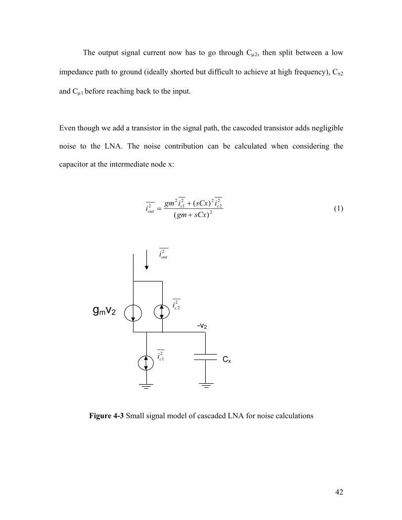
The output signal current now has to go through Cµ2, then split between a low
impedance path to ground (ideally shorted but difficult to achieve at high frequency), Cπ2
and Cµ1 before reaching back to the input.
Even though we add a transistor in the signal path, the cascoded transistor adds negligible
noise to the LNA. The noise contribution can be calculated when considering the
capacitor at the intermediate node x:
2
22
221
22
)()(
sCxgmisCxigm
i ccout +
+= (1)
Figure 4-3 Small signal model of cascaded LNA for noise calculations
22cigmv2
2outi
21ci
-v2
Cx

43
The output noise current is a function of collector current noise of transistors 1
and 2. If the parasitic capacitor Cx is kept small, the contribution of 22ci becomes
negligible. Ideally when Cx goes to zero, 2outi is only depended on the input transistor not
the cascoded one.
The cascode transistor increases the reverse isolation, does not introduce much
extra noise, and also improves the LNA’s gain. In fact, the highest achievable output
impedance is increased by a factor of β, greatly improves the gain of the LNA, even
though β ωT/ω at high frequency (see Figure 4-4 and equation (2) ). The devices in
these commercial technologies, the early effect and channel length modulation/DIBL are
significant, lowing ro at high frequency.
22 )1( oot
tout rr
iv
Z ββ ≈+== (2)
Figure 4-4 Output impedance of cascoded amplifier
gmv2 -v2
+ vt -
It
ro2rπ2
gmv1 ro1
44
4.3 Inductive Degenerated LNA Input Network
We investigate the input matching by considering the circuit of Figure 4-5. The
gain from vi to vo can be calculated as:
2
)(1
+++
−=
ose
L
i
o
jRCgmLj
gmRvv
ωωω π
(3)
π
ωCLL
wherebe
o )(1+
=
Figure 4-5 LNA small signal model to calculate input network
gmv1+ v1 -
vi
Zb
Ze
ZL
vo
Z

45
Equation (3) is a classical second order response with Q equal to
eoseo gmLRCgmLQ
ωω π 21
)(1
=+
= (4)
eTsse LRRCgmLwith ωπ == ,
The input matching Q and bandwidth is a function of gm or biasing only since ωo is fixed
and Le chosen to provide proper input matching impedance.
The voltage gain at ωo can be calculated yielding
so
TL
eo
LL
i
o
RR
LRQgmR
vv
ωω
ω 22−
=−
=−= (5)
Equation (5) shows that once again the gain is a function of fT, set by the biasing current,
which is the only design parameter of an impedance-matched L-degenerated LNA. To
improve the gain, one can increase fT and/or RL.
The unity gain frequency can only be increased at the expense of power
dissipation. Typically fT curve looks like the one shown in Figure 4-6. Ideally, one would
want to bias up the LNA transistor in the flat region where max fT and min NF are
achieved. Sometimes this current level dissipates too much power. More importantly the
high current roll-off region must be avoided because Kirk effect and high injection cause
significant distortion to the LNA, leading to poor IIP3 performance [10].
46
The second factor in the gain equation is the output impedance RL. Some effort is
put together to increase RL such as the use of cascoding. Using a pure resistive load helps
at the expense of voltage headroom and possible slow RC time constant. The use of
negative resistance at the output is discussed in [1] and shown in Figure 4-7. This
technique does make an improvement on the overall gain. It also makes the LNA a
variable gain amplifier (VGA) by varying the control voltage, Vgain. However with
additional devices added, NF also increases and also if the negative resistance is not well-
defined, the LNA could become unstable. The biggest drawback of this approach is the
poor linearity performance, since with high level of swing, possible latching could occur.
As a result, this technique is not employed in this design. To achieve high gain, focus is
placed on biasing transistors to obtain maximum fT, minimum NF, making high quality
passives and to use cascaded multi-stage design approach.
Figure 4-6 Unity gain frequency and NF Vs collector or drain current.
Ic or Id
fTNF

47
Figure 4-7 L-degenerated LNA with negative resistance generator at the output
4.4 Multi-stage LNA Topology
As we can see from the previous section, in order to achieve adequate gain, one
must be able to obtain max fT and/or output impedance. However, at the expense of
power dissipation, multiple stages can be used to improve overall gain. The proposed
topology used is shown in Figure 4-8, where the Q1 and Q2 are the L-degenerated LNA
with input power matched. Q3 and Q4 provide additional gain and reverse isolation. Note
that at the emitter of Q3, no inductive degeneration is used to maintain high gain
operation.
The additional devices Q3 and Q4 add negligible noise. As discussed in the
previous chapters, the NF of Q3 and Q4 will be divided by the power gain of Q1 and Q2.
RL CLL
Ls
RS Lg
out
Vdd
Vgain

48
Figure 4-8 2-stage LNA topology
Simulations show that Q3 and Q4 only contribute 5% more NF to the system.
Detailed results will be further discussed in later sections.
The inter-stage coupling capacitor, Cstage together with Cπ3 form a capacitive
divider. The impedance seen at the collector of Q2 is thus contributed from LC1 and the
transformed input equivalent parallel resistance of Q3 which is made large enough to not
to degrade the Q of the inductor significantly.
CCV
inV
outV
Rbias
Q1
Q3
Q2 Q4
2BV
Rbias
Lc1 Lc2
Le
Lb
1BV
Cstage
49
Besides having higher gain, multi-stage design can also provide higher bandwidth
than a single stage design. For a single stage design, the bandwidth of S21 depends on the
quality factor of the output tank. However with multi-stage design, one can purposely
adjust the center frequency of each stage to obtain a wideband response while scarifying
gain. A well-known technique is the stagger-tuning approach where the amplifier is
designed so that the overall response exhibits maximal flatness around the center
frequency fo [2]. A graphical representation of stagger-tuning is shown in Figure 4-9.
Figure 4-9 Stagger-tuning frequency response
1.414
1
22B
o −ω22
Bo +ωoω
.707 B
ω
H
Overall response

50
As we can see, the overall response has a flat gain region which is well-defined.
In the actual circuit implementation of the 30GHz LNA, the tank consisting of Lc1
together with Cstage and Cπ3 is tuned at ωo-B/2.83 and the output tank consisting of Lc2 and
the output capacitive divider is tuned at ωo+B/2.83.
Monte Carlo simulations show that stagger-tuning is less sensitive to component
variation. With 10% mis-matched between stages, the gain at the center frequency is still
well above adequate level and has a very tight standard derivation. As shown in Figure
4-10, the variance is placed only on the inductors for simulation purposes. This low
sensitive response is extremely desirable since at the carrier frequency of interest, any
mis-tuned narrow band response can cause functional failure whereas for a stagger-tuned
response, a flat gain response is achieved, allowing more tolerance.
Figure 4-10 Simulated gain distributions of 10% variations in LC1 and LC2
51
4.5 Passives Design
All the inductors used in this 30GHz LNA are implemented as coplanar
transmission lines with electrical length less than λ/4. A general transmission line has
input impedance equals to
ljZZljZZ
ZZinLo
oLo β
βtantan
++
= (6)
when the load is tied to an ideal ac ground equation (6) simplifies to:
ljZZin o βtan= (7)
As seen from equation (7) and Figure 4-11, as long as the transmission line length
is less than λ/4 or n*λ/4 for n is odd, it has a positive imaginary part which behaves like
an inductor. This implies that the self resonance frequency of this transmission line
inductor is very high compared to traditional spiral and/or loop on-chip inductors.
Figure 4-11 Short-circuited transmission line impedance
0 λ/4 λ/2 3λ/4 λ
Xin
length

52
With extensive electromagnetic field simulations, gap spacing is chosen such that
the transmission lines provide high characteristic impedance while highest quality factor
is obtained simultaneously. The lowest quality factor of these high impedance lines is still
greater than 15 at 30GHz, accounting for conductor, substrate and dielectric losses (see
Figure 4-12).
Both the quality factor and the inductance value are well-controlled due to the fact
that lithography in commercial process is precise to less than 0.2µm. This is a major
reason that coplanar lines are preferred over micro-strip lines which depend greatly on
the vertical oxide thickness that can vary a lot even with chemical mechanical polishing
at each metal deposition.
Figure 4-12 Typical transmission line simulation results
53
Another advantage of using coplanar transmission lines over inductive lines is
that the return currents are well-defined. If not carefully designed, these return paths can
introduce extra inductance. The ground metal layer is simulated with field solver and is
made very wide and very low impedance to reduce parasitic inductance.
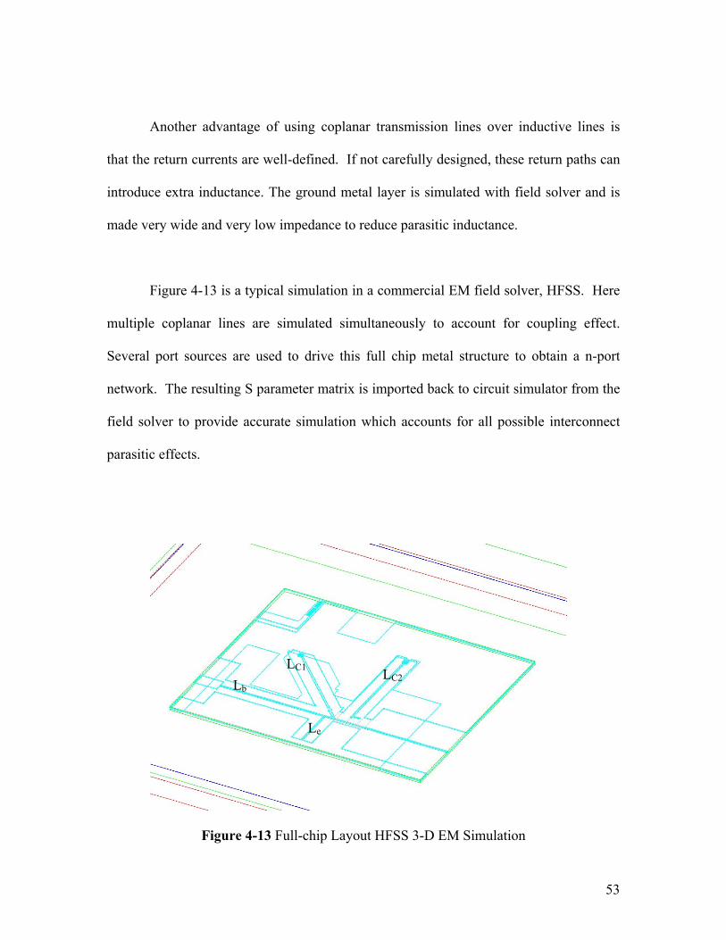
Figure 4-13 is a typical simulation in a commercial EM field solver, HFSS. Here
multiple coplanar lines are simulated simultaneously to account for coupling effect.
Several port sources are used to drive this full chip metal structure to obtain a n-port
network. The resulting S parameter matrix is imported back to circuit simulator from the
field solver to provide accurate simulation which accounts for all possible interconnect
parasitic effects.
Figure 4-13 Full-chip Layout HFSS 3-D EM Simulation
LC1 LC2
Le
Lb

54
4.6 LNA Simulation Performance
The LNA is implemented in a commercial SiGe BiCMOS process. The simulated
performance is summarized in Table 4-1.
Vcc 3V Icc 7.5mA S11 -35dB (min) S21 >20dB from (26G to 32G) S12 -65dB (max) S22 -15dB (min) NF 3.2dB P-1dB -20dBm (input referred)
Table 4-1 Simulated LNA performance
Simulation results show that due to accurate base and emitter inductance
modeling, very good input match is achieved. However, the transistor models which are
provided by the foundry may be inaccurate at high frequency which could cause gain to
be lower than expected. With stagger-tuning, broadband and high gain response is
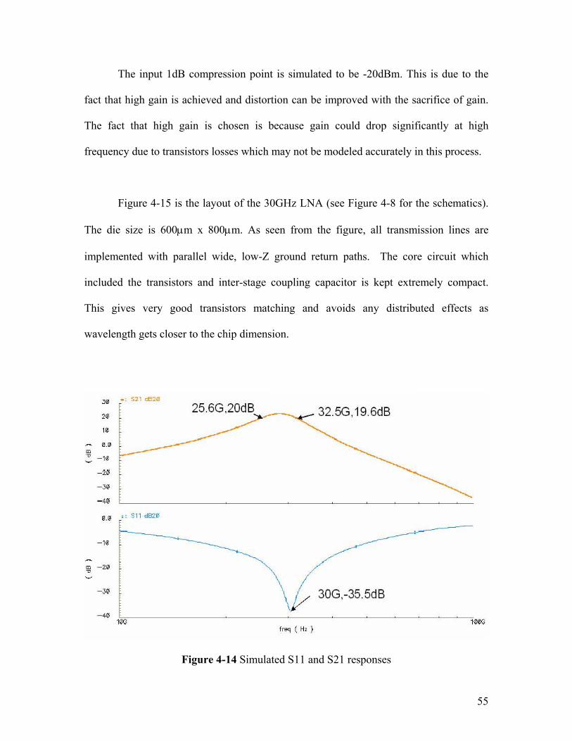
achieved. The maximum peak gain of 23.8dB, occurs at 29.7GHz, (see Figure 4-14)
which is 3dB lower per stage than the maximum gain, Gmax.
The noise figure of the 2-stage amplifier is simulated to be 3.2dB. This is within
0.5dB of the simulated minimum cascoded transistor’s NF at this frequency. This clearly
shows that the gain of the first stage overcomes the noise contribution from Q3 and Q4.
55
The input 1dB compression point is simulated to be -20dBm. This is due to the
fact that high gain is achieved and distortion can be improved with the sacrifice of gain.
The fact that high gain is chosen is because gain could drop significantly at high
frequency due to transistors losses which may not be modeled accurately in this process.
Figure 4-15 is the layout of the 30GHz LNA (see Figure 4-8 for the schematics).
The die size is 600µm x 800µm. As seen from the figure, all transmission lines are
implemented with parallel wide, low-Z ground return paths. The core circuit which
included the transistors and inter-stage coupling capacitor is kept extremely compact.
This gives very good transistors matching and avoids any distributed effects as
wavelength gets closer to the chip dimension.
Figure 4-14 Simulated S11 and S21 responses

56
Figure 4-15 Layout of the 30GHz LNA
The power supply metal layer is heavily bypassed because VCC is also tied to the
cascode transistor’s base. The input and output pad structures are designed and simulated
in EM field solver (see Figure 4-13). The simulated s-parameters are then imported back
to schematic as part of the input and output matching networks.
The design of a fully-integrated, broadband, low-power 30GHz LNA is
demonstrated. The use of distributed elements such as transmission lines is discussed.
The designs of cascading, biasing, matching and multi-stage tuning are also investigated
in this chapter.
LC1
Lb
LC2
Le
57
References [1] Chung-Yu Wu and Shuo-Yuan Hsiao, “The Design of a 3-V 900-MHz CMOS Bandpass Amplifier,”
IEEE JOURNAL OF SOLID-STATE CIRCUITS, VOL. 32, NO. 2, FEBRUARY 1997
[2] Sedra and Smith , Microelectronic circuits, Oxford University Press
[3] David Pozar, Microwave Engineering, John Wiley & Sons; 2nd Edition
[4] Xiaomin Yang, Thomas Wu and John McMacken, “Design of LNA at 2.4GHz Using 0.25um
Technology,” Silicon Monolithic Integrated Circuits in RF Systems, 2001
[5] Guillermo Gonzalez, Microwave Transistor Amplifiers Analysis and Design, Prentice Hall PTR; 2nd
edition
[6] R. Rafla and M.El-Gamal, “Design of a 1.5V CMOS Integrated 3GHz LNA,” ISCAS 99, Vol. II, pp.
440-443, June 1999
[7] D.K. Shaeffer and T.H. Lee, “A 1.5V, 1.5GHz CMOS Low Noise Amplifier,” IEEE Journal of Solid-
State Circuits, VOL. 32, No.5 May 1997
[8] Paul Gray and Robert Meyer, Analysis and Design of Analog Integrated Circuits, John Wiley & Sons;
3rd edition
[9] Thomas Lee, The Design of CMOs Radio Frequency Integrated Circuits, Cambridge Univ Pr
[10] Robert Meyer, EE242 Lecture Notes
[11] Yongwang Ding, Ramesh Harjani, “A +18dBm IIP3 LNA in a 0.35um CMOS,” Solid-State Circuits
Conference, 2001
[12] R.C Liu, C.R Lee, H. Wanf and C.K. Wang, “A 5.8GHz Two-Stage High-Linearity Low Voltage low
Noise amplifier in a 0.35um CMOS Technology,” 2002 IEEE RFIC Symposium

58
Chapter 5
Microwave Frequency Dividers
5.1 Introduction
The growing importance of wireless systems, from cell phone to wireless local
area network, is driving the need for higher performance and lower power dissipation. In
particular for the 60GHz WLAN project, power dissipation is a major concern. As
carrier frequency gets higher, power dissipation also increases proportionally. In this
chapter, a major power consumption block, the frequency divider, is investigated as part
of a frequency synthesizer loop. Static frequency divider design and its pros/cons are
discussed. Low power and high frequency divider design techniques are described later
in the chapter.
Figure 5-1 Typical wireless transceiver system
LNA Filter ADC IF AMP
DAC
Duplexer
PA Filter
IF AMP Freq Syn.

59
5.2 Frequency Synthesizers
To understand the fundamentals of frequency divider, we first discuss the role of
frequency synthesizer. The function of an ideal synthesizer is to generate a single tone at
a frequency spectrum of fLO= fRF-fIF which is used for frequency modulation in a wireless
transceiver. A typical receive and transmit wireless block diagram is shown in Figure 5-1.
Figure 5-2 Frequency spectrum modulation
f
SRX(f)
fRF
f
SLO(f)
fLO
f
SIF(f)
fIF
f
SIF(f)
fIF
f
SLO(f)
fLO
f
STX(f)
fRF
interferer
interferer

60
The frequency synthesizer plays a key role in both the RX and TX paths. The
synthesizer together with the mixer translate RF carrier signal to baseband IF signal. In
the receiver case, the synthesized LO tone mixes with the RF signal spectrum and
translates it down to baseband signal. In the transmitter case, it mixes with the modulated
baseband signal and shifts it up to RF [1] Figure 5-2 shows the graphical representation
of the synthesizer’s role in a transceiver.
As shown in Figure 5-3, a frequency synthesizer consists of a phase/frequency
detector (PFD), loop filter, voltage-controlled oscillator (VCO) and a frequency divider.
The basic task of a PLL is to generate a clean signal at frequency fLO by locking
the low noise reference crystal oscillator (typically in MHz frequency range), fref, to the
tunable free running signal fLO.
Figure 5-3 Block diagram of a PLL synthesizer
PFD Loop filter VCO
÷N
fref
fLO/N
fLO Vcontrol

61
The phase/frequency detector compares the divided frequency fLO/N to fref. The
low-pass filter selects the difference voltage signal that is almost at DC when the two
frequencies are close to each other (fref ~ fLO/N). This DC-like signal is controlling the
charge pump (not shown in figure) that increases or decreases the voltage Vcontrol. The
output frequency of the VCO is set by Vcontrol, which can be expressed
controlVCOrunningfreeLO VKωω ×+= − (1)
where Kvco is the VCO’s gain [rad/s/volt]
The loop filter sets the bandwidth, thus the noise and transient dynamics
performance of the entire loop. Figure 5-4 illustrates the linear transfer function block
diagram of the synthesizer.
Figure 5-4 Transfer function of synthesizer
KD F(s) KVCO
1/N
φref
φLO/N
ωLO +
-
1/s φLO

62
Solving the TF block gives:
)(1)(
)()(
)()(
sTsTN
NKsFK
s
KsFKs
KsFKN
VCOD
VCOD
ref
LO
LOVCODLO
ref
+=
+=
=×−
φφ
φφ
φ
(2)
wheresNKsFK
sT VCOD
×=
)()(
Equation (2) is the closed loop response of the synthesizer, containing the loop gain, T(s),
which has a typical feedback loop expression.
As in any feedback loop system, stability is a concern. An inherent pole at DC is
present due to the fact that frequency is the rate of change of phase with time [2] [5]
dtdφω = or in s-domain φω
=s
This inherent pole together with other parasitic poles in the loop can cause
instability if the loop filter is not carefully designed.
When F(s) is simply a first order low-pass filter with transfer function,
1
1
1)(
p
ssF
ω+
=

63
Figure 5-5 (a) Magnitude and phase responses of T(s); (b) Root Locus of T(s); (c) Root
Locus of T(s) with a parasitic pole present
the loop gain, T(s), becomes a 2nd order function that could lead to 0o phase margin and
possibly instability as the complex conjugate poles cross the imaginary axis see Figure 5-
5 [2]. This corresponds to excess overshoot and ringing in the time domain.
As a result, compensation technique must be applied by introducing a zero in the filter
transfer function, yielding
1
1
1
1)(
p
z
s
s
sF
ω
ω
+
+=
the loop gain, T(s), becomes stable with judiciously placement of a zero, ωz1, on the left
hand plane, see Figure 5-6
|T(s)|
ω
∠T(s)
ωp1
ω
Kv
0o
X X
Im
Re
Im
ReX X X
parasitic pole
Fig. 5a
Fig. 5b
Fig. 5c
-20dB/dec
~0o phase margin
-40dB/dec

64
Figure 5-6 (a) Magnitude and phase responses of T(s); (b) Root Locus of T(s); (c) Root
Locus of T(s) with a parasitic pole present
5.3 Wideband Frequency Dividers
The previous section explores the basic operation of a synthesizer, and this
section will focus on the frequency divider block. The role of a divider is to translate fLO
to fref by a ratio N. In most wireless systems, fLO >> fref . This is a common situation due
to the fact that fLO is close to the carrier frequency, in the order of GHz range and that fref
is generated from a crystal oscillator that is practical in the MHz range, limited by
ω
|T(s)|
∠T(s) ωp1
ω
Kv
-90o -180o
0o
Im
Re
Fig. 6a
Fig. 6b
Fig. 6c
-20dB/dec -40dB/dec
ωz1
Crossover frequency
Im
Reo X X
X o X X parasitic pole
65
crystal’s physical size and stability. Therefore a large division ratio N is usually required,
especially in the 60GHz transceiver.
From Figure 5-3, we can clearly identify that the highest frequency blocks of a
synthesizer are the VCO and the divider. For an oscillator to function in a given
technology, it is necessary to have fmax, the maximum unity power gain frequency, to be
greater than fLO. Depending on the output to input impedance ratio, some processes like
SiGe and GaAs, fmax could be greater than the unity current gain frequency, fT [4].
While VCOs operate at the maximum frequency of a technology, dividers cannot.
Also large division ratio N may be required as carrier frequency gets higher, possibly
many stages of dividers are needed, making the divider one of the major sources of power
dissipation in the frequency synthesizers [3]. To combat this problem, the techniques of
designing low-power and high speed dividers are carefully investigated.
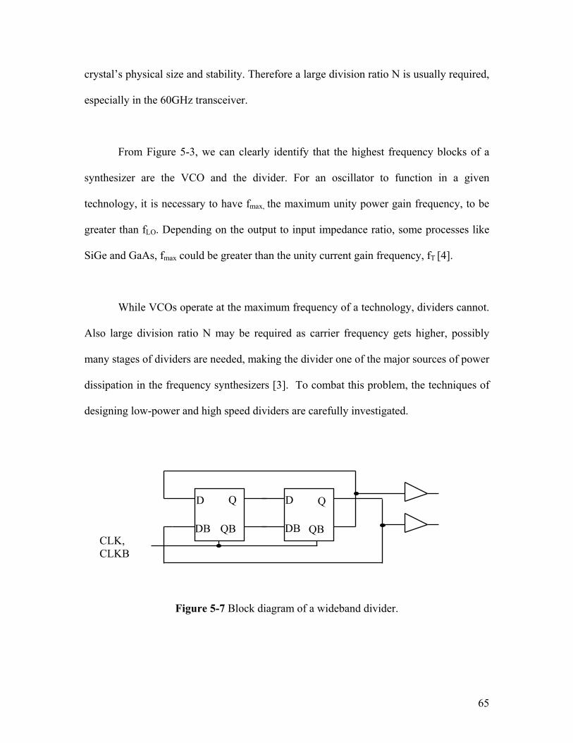
Figure 5-7 Block diagram of a wideband divider.
D
DB
Q
QB
D
DB
Q
QBCLK, CLKB

66
The existing dividers can be categorized into 2 types: digital wideband and analog
based narrow-band dividers. The wideband divider is first investigated and the analog
based divider is discussed in the next chapter. The digital divider consists of two D
latches cascaded with the inverted output feeding back to the non-inverting input of the
fist latch, forming a master-slave configuration (see Figure 5-7).
The first latch is transparent when CLK is “high” and holds the previous values
when CLK is “low.” The second latch operates the exact opposite. At the frequency of
interest, “high” corresponds to the positive or raising portion of the input clock sine
wave, and “low” corresponds to the negative portion. The simulated transient operation
of frequency division is shown in Figure 5-8. The output frequency is exactly half of the
input frequency, thus a division ratio of 2 is achieved.
Figure 5-8 Timing operations of divider

67
Figure 5-9 D latch implementation
The D latch is realized with emitter coupled logic or ECL (see Figure 9). The
differential pair is operating as a current steering device, switching Itail between Q1 and
Q2. Q3 and Q4 are cross-coupled pair or latching-pair, providing negative resistance to
further increase or decrease the voltage at Q and QB.
A well-known hyperbolic tangent large signal transfer function of a BJT
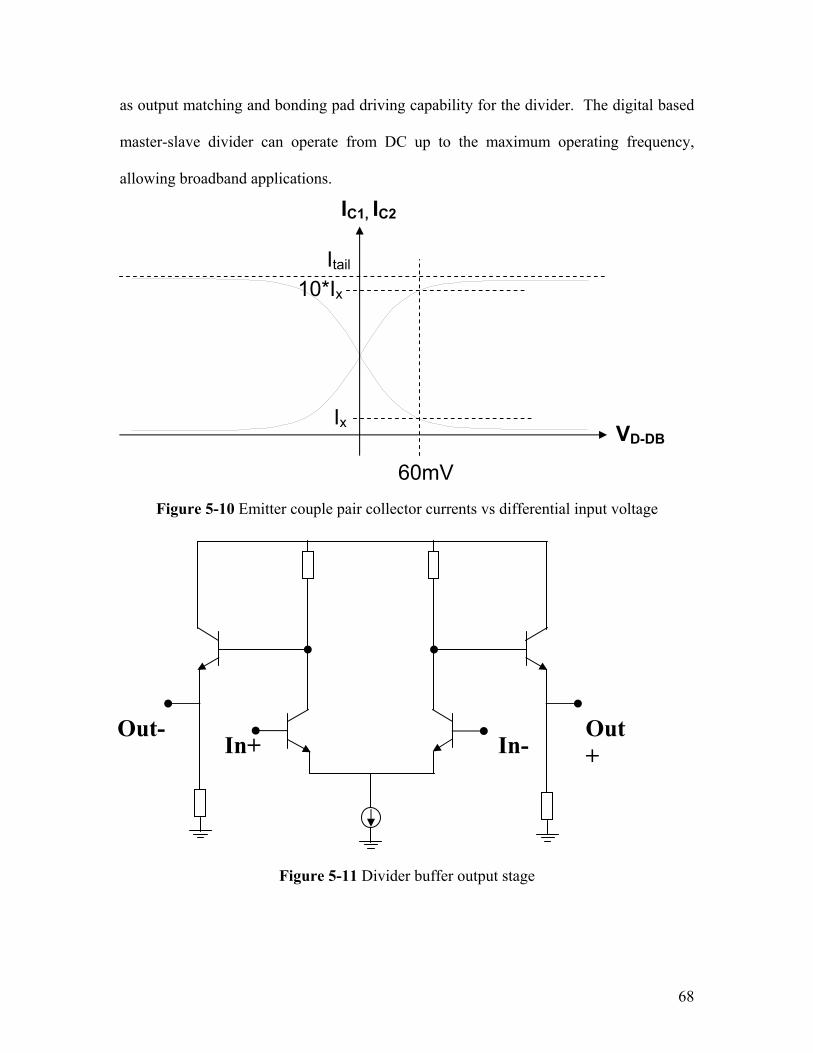
differential pair is shown in Figure 5-10. When a 60mV differential signal is applied to
the input, a 10:1 current ratio is achieved. This results in a higher sensitivity than an ideal
MOS differential input pair.
The highest frequency operation is clearly set by the two delays of the latches
which is a function of device biasing and parasitic load at the output. With proper
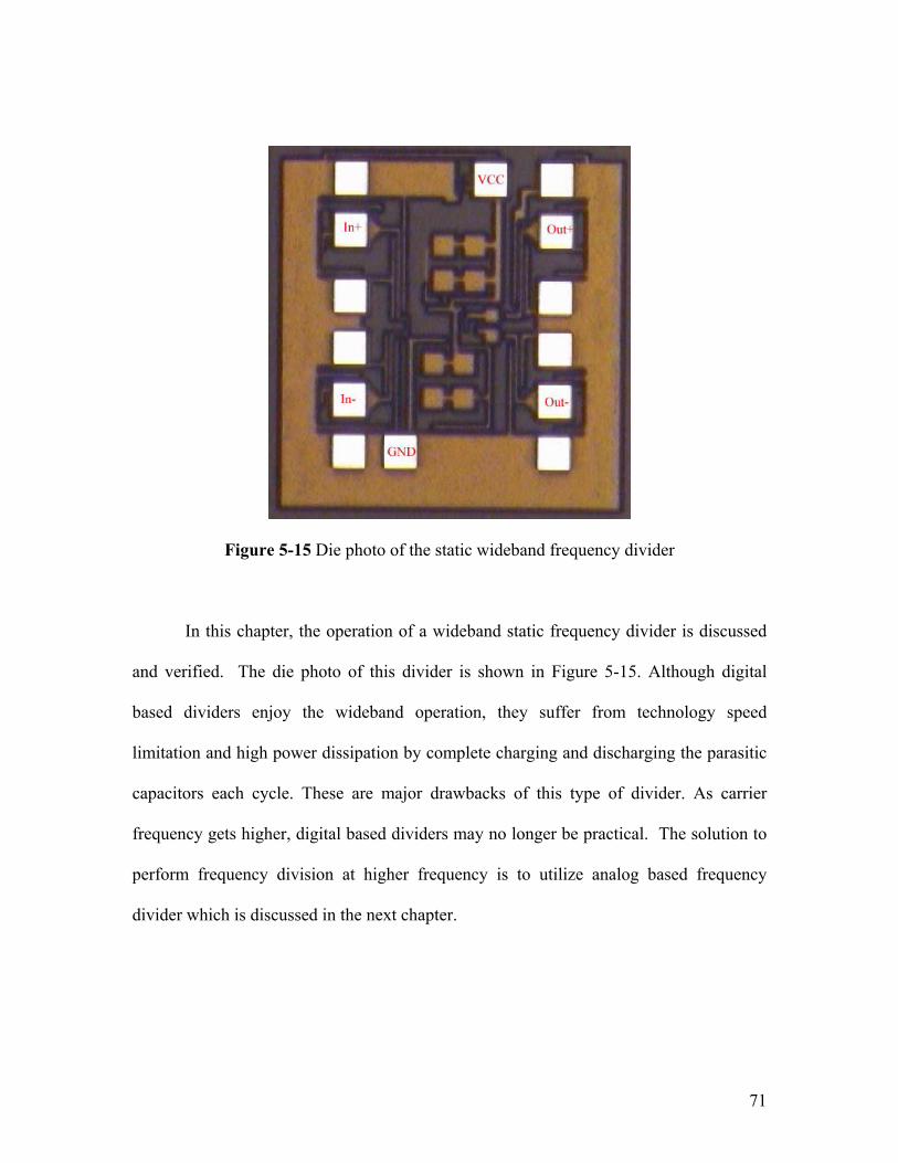
transistor sizing and biasing, speed and power tradeoff can be optimized. Buffers are used
to lessen the 50Ω off-chip output load, see Figure 5-11. The buffers provide gain as well
DB
CLK CLKB
QBQ
VCC
Q1 Q2D
Q3 Q4
Itail
68
as output matching and bonding pad driving capability for the divider. The digital based
master-slave divider can operate from DC up to the maximum operating frequency,
allowing broadband applications.
Figure 5-10 Emitter couple pair collector currents vs differential input voltage
Figure 5-11 Divider buffer output stage
In+ In-Out+
Out-
VD-DB
IC1, IC2
Itail
60mV
10*Ix
Ix

69
5.4 Measurement Results of Wideband Frequency Dividers
A prototype divider is implemented in a 120GHz fT SiGe process. The operation
of divider is verified up to 20GHz and it dissipates 20.2mW including the output buffer
which dissipates 17mW. Typical measurement results are shown in Figures 5-12 and 13.
Power Dissipation Vs Input Frequency
17.518
18.519
19.520
20.5
0 5 10 15 20
Frequency (GHz)
Pow
er (m
W)
Figure 5-12 Power Dissipation vs Frequency of digital divider
Minimum Input Power VS Frequency
-20-15-10
-505
101520
5 8 10 12 14 16 18 20
Frequency (GHz)
Pin
(dB
m)
min Pin (low Re)min Pin
min output power of generator=-15dBm
Figure 5-13 Input Power vs Frequency of divider

70
Simulation shows this divider is operational up to 30GHz. The measured upper
operational frequency of this divider is limited by the test equipment. The signal
generator used, HP83711B, can only output signal up to 20GHz. In addition to that, the
cable and the off-chip bias-T insertion losses are quite significant. The measured cable
insertion loss is about -4dB and the bias-T loss is plotted in Figure 5-14. A Mini-Circuits
15542 bias-T is used for measurement, which has a datasheet specification of 1.3dB or
less insertion loss from 100kHz to 6GHz.
Bias T Insertion Loss Vs Frequency
-9-8-7-6-5-4-3-2-10
1 2 4 6 10 12 14 16 18 20
Frequency (GHz)
IL (d
B) Bias-T IL spec up to 6GHz
Figure 5-14 Insertion Loss vs Frequency of bias T
71
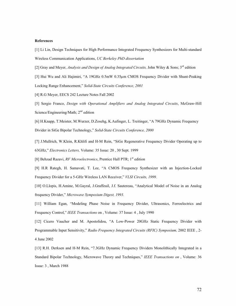
Figure 5-15 Die photo of the static wideband frequency divider
In this chapter, the operation of a wideband static frequency divider is discussed
and verified. The die photo of this divider is shown in Figure 5-15. Although digital
based dividers enjoy the wideband operation, they suffer from technology speed
limitation and high power dissipation by complete charging and discharging the parasitic
capacitors each cycle. These are major drawbacks of this type of divider. As carrier
frequency gets higher, digital based dividers may no longer be practical. The solution to
perform frequency division at higher frequency is to utilize analog based frequency
divider which is discussed in the next chapter.
72
References
[1] Li Lin, Design Techniques for High Performance Integrated Frequency Synthesizers for Multi-standard
Wireless Communication Applications, UC Berkeley PhD dissertation
[2] Gray and Meyer, Analysis and Design of Analog Integrated Circuits, John Wiley & Sons; 3rd edition
[3] Hui Wu and Ali Hajimiri, “A 19GHz 0.5mW 0.35µm CMOS Frequency Divider with Shunt-Peaking
Locking Range Enhancement,” Solid-State Circuits Conference, 2001
[4] R.G Meyer, EECS 242 Lecture Notes Fall 2002
[5] Sergio Franco, Design with Operational Amplifiers and Analog Integrated Circuits, McGraw-Hill
Science/Engineering/Math; 2nd edition
[6] H.Knapp, T.Meister, M.Wurzer, D.Zosehg, K.Aufinger, L. Treitinger, “A 79GHz Dynamic Frequency
Divider in SiGe Bipolar Technology,” Solid-State Circuits Conference, 2000
[7] J.Mullrich, W.Klein, R.Khlifi and H-M Rein, “SiGe Regenerative Frequency Divider Operating up to
63GHz,” Electronics Letters, Volume: 35 Issue: 20 , 30 Sept. 1999
[8] Behzad Razavi, RF Microelectronics, Prentice Hall PTR; 1st edition
[9] H.R Rategh, H. Samavati, T. Lee, “A CMOS Frequency Synthesizer with an Injection-Locked
Frequency Divider for a 5-GHz Wireless LAN Receiver,” VLSI Circuits, 1999.
[10] O.Llopis, H.Amine, M.Gayral, J.Graffeuil, J.f. Sautereau, “Analytical Model of Noise in an Analog
frequency Divider,” Microwave Symposium Digest, 1993.
[11] William Egan, “Modeling Phase Noise in Frequency Divider, Ultrasonics, Ferroelectrics and
Frequency Control,” IEEE Transactions on , Volume: 37 Issue: 4 , July 1990
[12] Cicero Vaucher and M. Apostolidou, “A Low-Power 20GHz Static Frequency Divider with
Programmable Input Sensitivity,” Radio Frequency Integrated Circuits (RFIC) Symposium, 2002 IEEE , 2-
4 June 2002
[13] R.H. Derksen and H-M Rein, “7.3GHz Dynamic Frequency Dividers Monolithically Integrated in a
Standard Bipolar Technology, Microwave Theory and Techniques,” IEEE Transactions on , Volume: 36
Issue: 3 , March 1988
73
Chapter 6
Injection-Locked Frequency Dividers
6.1 Introduction
In the previous chapter, we introduced wideband digital based dividers. This type
of divider is widely used in frequency synthesizers even though it can be extremely
power hungry at high frequency. In the 60GHz WLAN transceiver, digital-based dividers
will not be the preferable choice not only because they dissipate too much power, but in
fact these dividers simply cannot operate at the LO frequency with the given commercial
CMOS and SiGe processes. As a result, analog-based dividers must be considered as one
of the building blocks in the transceiver. In particular, a regenerative divider, the
injection-locked frequency divider is explored. In this chapter, we will first introduce the
concept of a regenerative divider, then the injection-locking phenomenon, and finally the
design techniques of injection-locked frequency divider (ILFD) are investigated.
6.2 Regenerative Divider
R.L. Miller originally proposed the regenerative divider method in 1939 [1]. This
analog-based divider utilizes a mixer and a low pass filter to obtain fraction of the input
frequency at the output. As shown in Figure 6-1, the input frequency is fed into a mixer,
which produces both the sum and difference frequencies at fin ± fout. This mixed signal is
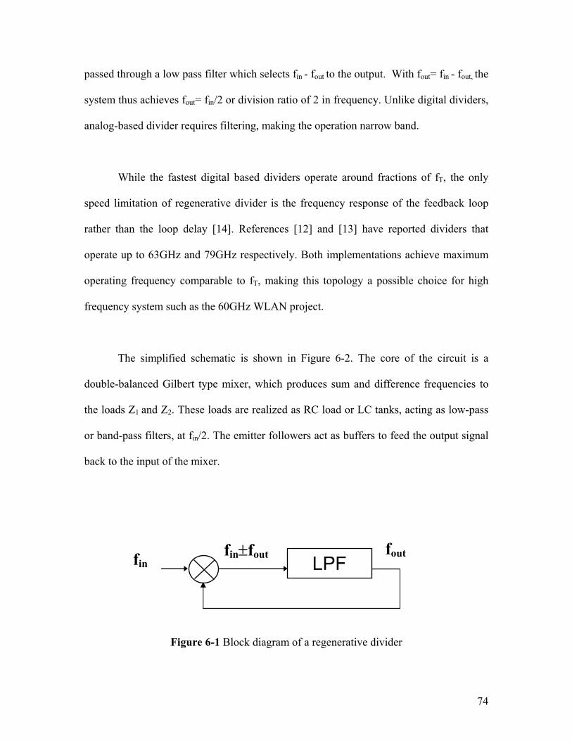
74
passed through a low pass filter which selects fin - fout to the output. With fout= fin - fout, the
system thus achieves fout= fin/2 or division ratio of 2 in frequency. Unlike digital dividers,
analog-based divider requires filtering, making the operation narrow band.
While the fastest digital based dividers operate around fractions of fT, the only
speed limitation of regenerative divider is the frequency response of the feedback loop
rather than the loop delay [14]. References [12] and [13] have reported dividers that
operate up to 63GHz and 79GHz respectively. Both implementations achieve maximum
operating frequency comparable to fT, making this topology a possible choice for high
frequency system such as the 60GHz WLAN project.
The simplified schematic is shown in Figure 6-2. The core of the circuit is a
double-balanced Gilbert type mixer, which produces sum and difference frequencies to
the loads Z1 and Z2. These loads are realized as RC load or LC tanks, acting as low-pass
or band-pass filters, at fin/2. The emitter followers act as buffers to feed the output signal
back to the input of the mixer.
Figure 6-1 Block diagram of a regenerative divider
LPF fin fin±fout fout

75
Figure 6-2 Simplified Schematic of Regenerative divider
The major drawback of regenerative divider is high power consumption, both
implementations [12] [13] dissipate up to 10 times higher power than digital based
divider would at the same operating frequency using special technology such as GaAs or
InP. One of the major sources of power dissipation is in the buffer feedback stage that has
to provide enough swing to fully switch input differential pairs while achieving optimal
frequency response. In general, unlike Figure 6-2, multiple Darlington emitter follower
configurations have to be realized to provide proper DC level shifting and reduce high
frequency parasitic loading effect.
+ Output -
+ Input -
Z1
Z2

76
To resolve this high power dissipation problem, the injection locked frequency
divider is proposed. This architecture is similar to regenerative divider where it is analog-
based, narrow band and can achieve high frequency of operation. As describe in the next
section, a free-running oscillator is locked to an external input frequency to achieve
frequency division. This approach not only achieves adequate frequency of operation but
it also enjoys lower power dissipation and low phase noise degradation.
6.3 Theory of Injection Locking
To understand ILFD, we have to first understand the origin of injection locking.
In oscillator design, injection locking is a well-known phenomenon. When a free-running
oscillator, operating at frequency f1, is being coupled intentionally or unintentionally by
an external incident signal, at frequency f2, eventually the oscillator is locked to the
injected signal at frequency f2, if f1~f2 and the injected signal has coupled enough energy
to the oscillator. This occurrence is sometimes known as injection-pulling or LO-pulling.
In most practical situations, LO-pulling is an undesirable phenomenon. One such
example occurs in a direct conversion transmitter where the RF carrier frequency is equal
to the LO frequency, see Figure 6-3. This architecture suffers from a drawback that there
is disturbance of LO signal from the power amplifier [1].

77
Figure 6-3 Direct Conversion System
The PA, which produces large output signal to the antenna at fRF may leak and
couple portion of the signal through the conductive substrate or other parasitic path back
to the local oscillator, causing injection locking. This is extremely undesirable since the
signal at the output of the PA contains modulated baseband information, which is
centered at the carrier frequency fRF. This “noisy” modulated spectrum is also centered at
fLO, corrupting the clean low phase noise oscillator as a result. When the local oscillator
is locked to this modulated signal, phase noise performance degrades significantly.
To alleviate this problem, careful shielding should be employed or different
frequency planning can be utilized as in Figure 6-4. The local oscillator is operating at a
fraction of the actual LO frequency, 2/3 fLO in this case, and is mixed with its own
divided-by-2 signal to produce fLO and 1/3 fLO. After filtering, fLO is generated. This
method separates the PA modulated high power signal from the LO frequency by 1/3 LO,
thus avoiding injection locking.
coupling
DAC PAfRF
fLO
fIF=DC

78
Figure 6-4 Fractional Frequency Generation
6.4 Introduction of Injection Locked Frequency Divider
We have seen the problems that injection locking can cause to a system, but
utilizing the very same principle, we can take advantage of injection locking. In
particular, when a high phase noise free-running oscillator is being locked by an accurate
and low noise signal, the oscillator eventually produces a well-defined and low noise
output tone. With that in mind, applying the regenerative divider concept, ILFD can be
realized as in Figure 6-5 [2].
Figure 6-5 Block Diagram of ILFD [2]
÷2
≈LOf
32
=
LOf31
=
LOLOf ,31
=
LOf =
Nonlinear Element
Gain Resonator
Injected signal
fo=fi/2
fi/2
fi fi/2, 3fi/2,…
oscillator core
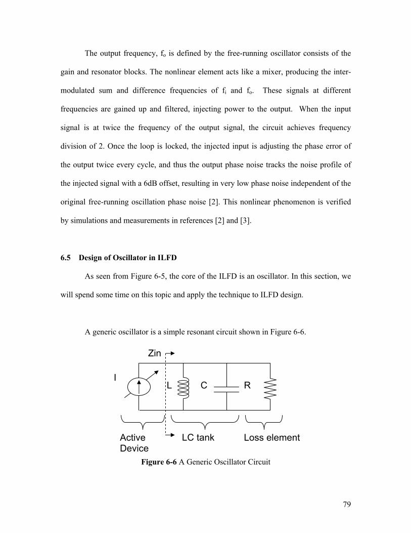
79
The output frequency, fo is defined by the free-running oscillator consists of the
gain and resonator blocks. The nonlinear element acts like a mixer, producing the inter-
modulated sum and difference frequencies of fi and fo. These signals at different
frequencies are gained up and filtered, injecting power to the output. When the input
signal is at twice the frequency of the output signal, the circuit achieves frequency
division of 2. Once the loop is locked, the injected input is adjusting the phase error of
the output twice every cycle, and thus the output phase noise tracks the noise profile of
the injected signal with a 6dB offset, resulting in very low phase noise independent of the
original free-running oscillation phase noise [2]. This nonlinear phenomenon is verified
by simulations and measurements in references [2] and [3].
6.5 Design of Oscillator in ILFD
As seen from Figure 6-5, the core of the ILFD is an oscillator. In this section, we
will spend some time on this topic and apply the technique to ILFD design.
A generic oscillator is a simple resonant circuit shown in Figure 6-6.
Figure 6-6 A Generic Oscillator Circuit
I L C R
Active Device
LC tank Loss element
Zin
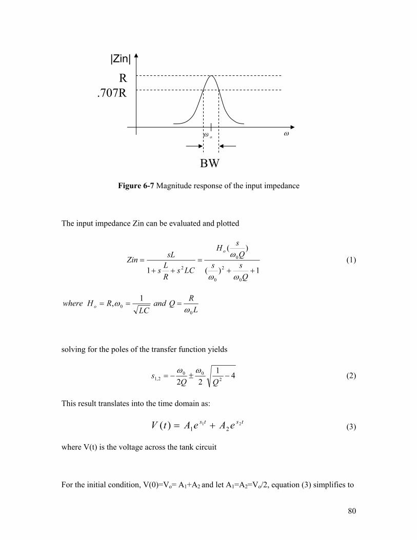
80
Figure 6-7 Magnitude response of the input impedance
The input impedance Zin can be evaluated and plotted
1)(
)(
10
2
0
0
2 ++=
++=
QssQ
sH
LCsRLs
sLZino
ωω
ω (1)
LRQand
LCRHwhere o
00
1,ω
ω ===
solving for the poles of the transfer function yields
4122 2
002,1 −±−=
QQs
ωω (2)
This result translates into the time domain as:
tsts eAeAtV 2121)( += (3)
where V(t) is the voltage across the tank circuit
For the initial condition, V(0)=Vo= A1+A2 and let A1=A2=Vo/2, equation (3) simplifies to
oω ω
|Zin|
R .707R
BW
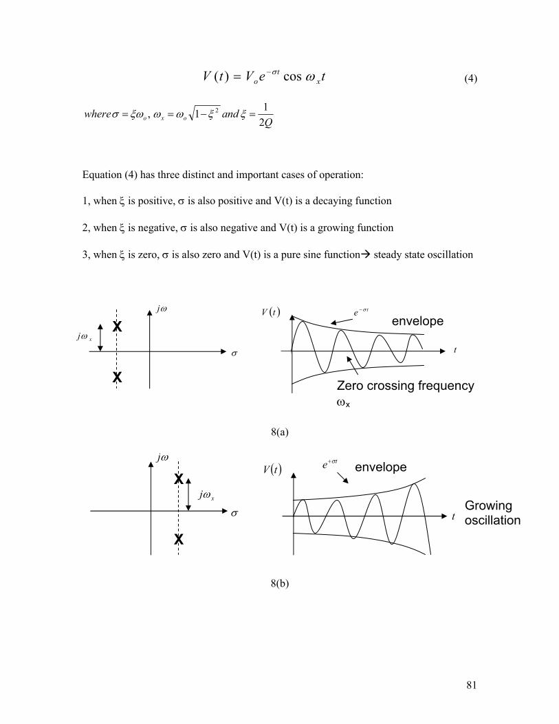
81
teVtV xt
o ωσ cos)( −= (4)
Qandwhere oxo 2
11, 2 =−== ξξωωξωσ
Equation (4) has three distinct and important cases of operation:
1, when ξ is positive, σ is also positive and V(t) is a decaying function
2, when ξ is negative, σ is also negative and V(t) is a growing function
3, when ξ is zero, σ is also zero and V(t) is a pure sine function steady state oscillation
8(a)
8(b)
X
X xjω
( )tV te σ−
envelope
Zero crossing frequency ωx
t
ωj
σ
Growing oscillation
X
X ( )tV
te σ+ envelope
t
ωj
σxjω

82
8(c)
Figure 6-8(a) Root locus and transient response of case 1; 8(b) case 2 and 8(c) case 3.
Clearly for oscillation to occur, the circuit must be able to locate the complex
conjugate poles to the right of the imaginary axis during start up (case 2) and then locate
the poles on the imaginary axis during steady state (case 3).
For this to happen, the quality factor, Q, which is defined as [4]
ondperlossenergystoredenergy
sec)(*Q ω
= (5)
has to be ∞ at resonance. We can intuitively note that the circuit must be able to provide
energy to the circuit exactly equal to the energy loss every cycle. This also implies that
active device(s) must be utilized in any oscillator. To accomplish that we will examine
the single transistor oscillator and then a differential approach is investigated. As we will
see, we can readily implement the ILFD from these oscillator topologies.
( )tV
t
ωx= ωo oV
X
X ωj
σojω
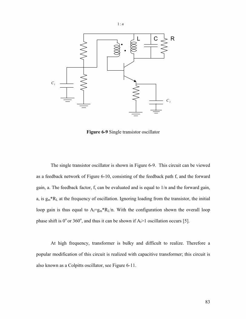
83
Figure 6-9 Single transistor oscillator
The single transistor oscillator is shown in Figure 6-9. This circuit can be viewed
as a feedback network of Figure 6-10, consisting of the feedback path f, and the forward
gain, a. The feedback factor, f, can be evaluated and is equal to 1/n and the forward gain,
a, is gm*RL at the frequency of oscillation. Ignoring loading from the transistor, the initial
loop gain is thus equal to Al=gm*RL/n. With the configuration shown the overall loop
phase shift is 0o or 360o, and thus it can be shown if Al>1 oscillation occurs [5].
At high frequency, transformer is bulky and difficult to realize. Therefore a
popular modification of this circuit is realized with capacitive transformer; this circuit is
also known as a Colpitts oscillator, see Figure 6-11.
L C R
•
•
1C
n:1
2C

84
Figure 6-10 Simplified block diagram
For the Colpitts oscillator or any oscillators, the initial loop gain must be designed
to be sufficient enough such that start up is guaranteed and not too excessive to avoid
latching. To achieve that, one should pick Al ~3 to 5 [5].
Figure 6-11 Colpitts Oscillator Circuit
R C L
1:n ••
Gain = a
f=1/n
EI
2C
1C
3C L
1/Gm

85
The major drawback of the Colpitts oscillator is that the loading from the active
device is quite significant. Accounting for loading, the loop gain can be solved, yielding
2
1n
)gmR(n-Al = (6)
by taking the differential of gmR and solve for the optimal transform ratio n:
02)1(
))1()1(2()( 2
=−
−−=
n
nnnAdngmRd
l (7)
2=optn
When Al≥1, n=2, minimum gmR must be greater than or equal to 4 [6]. This may not
seem like much gain; however with finite on-chip passives Q and transistors operating
close to fmax during resonance, this could be difficult to achieve.
Figure 6-12 is a differential oscillator, which does not suffer from this gain
limitation. This configuration is sometimes known as the negative resistance oscillator
because the impedance looking into the two cross-coupled transistors is Rneg = –2/gm.
This negative impedance “cancels” the losses introduced by the finite Q of the inductors,
capacitors and also the gate resistance and substrate loss of the transistor. The loop gain
of this oscillator is Al=(gm*Rp)2 and oscillation occurs when Al≥1, implying gm*Rp≥1.

86
As indicated, not only does this differential oscillator have lower gain
requirement, but this configuration also provides a natural divided-by-2 injection point
[2]. At the sources of the cross-coupled transistors, node X of Figure 6-12, the frequency
of oscillation is at twice the frequency of the output, due to the fact that each transistor
conducts half of the cycle and acts as a source follower when conducting. Even though
the voltage waveform at node X is not a sinusoidal signal but a rectified one, it consists of
rich second harmonic and other even harmonic tones, making injection locking easier to
realize. Therefore a differential topology is chosen to be the oscillator of ILFD.
Figure 6-12 Differential Oscillator
L LC
Rneg
RpRp
x
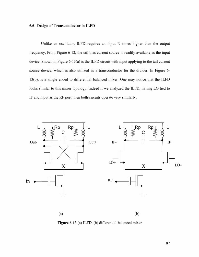
87
6.6 Design of Transconductor in ILFD
Unlike an oscillator, ILFD requires an input N times higher than the output
frequency. From Figure 6-12, the tail bias current source is readily available as the input
device. Shown in Figure 6-13(a) is the ILFD circuit with input applying to the tail current
source device, which is also utilized as a transconductor for the divider. In Figure 6-
13(b), is a single ended to differential balanced mixer. One may notice that the ILFD
looks similar to this mixer topology. Indeed if we analyzed the ILFD, having LO tied to
IF and input as the RF port, then both circuits operate very similarly.
(a) (b)
Figure 6-13 (a) ILFD, (b) differential-balanced mixer
L LC
Rp Rp
x
RF
IF- IF+
LO-LO+
L LC
Rp Rp
x
in
Out- Out+

88
The tail current source/transconductor should be implemented with multi-finger
transistor to reduce gate resistance Rg of equation 7 which is inversely proportional to n2.
LnWR
R sqg 2= (7)
Also the biasing level is chosen for adequate initial loop gain and unit-gain
frequency of the transistor since the input of the ILFD circuit is at the highest frequency.
By acquiring the biasing level and the Q of the LC tank, the output amplitude is defined.
In the case of divide-by-two, it can be shown that the locking range of the ILFD is
[7]
|2
||| 2
QVaH io
r
<∆ωω (8)
where
∆ω frequency offset from ωr;
ωr free-running oscillation frequency;
Vi incident amplitude;
Ho impedance of the RLC tank at resonance;
Q quality factor of the RLC tank;
a2 second-order coefficient of the non-linearity.
The higher the input amplitude, second-order distortion and tank impedance, the
higher the locking range will be. Also lowering the Q of the tank helps to improve
locking range because it makes the output response more broadband. This low Q tank

89
doesn’t degrade the phase noise performance after injection-locking, because as
mentioned earlier, the free-running jitter is adjusted by the incident input twice every
cycle; therefore the output phase noise tracks the input noise profile.
The second order coefficient is produced when the transconductor’s output
current is mixed with the differential pair’s harmonics. The ideal switching differential
pair has the transfer function:
....)5cos513cos
31(cos2
211 ttt
II
SS
d ωωωπ
+−+= (9)
which contains the fundamental, and odd harmonics only. Even harmonics exists only in
non-ideal situation, caused by mismatches between the devices. The tail current Iss has
input signal at 2ω in the divided-by-2 case
tII iSS ω2cos= (10)
substituting equation (10) into (9) yields:
tItttI id ωωωωπ
2cos*....)]5cos513cos
31(cos2
21[1 +−+=
)...)23(cos31)2((cos
22cos ωωωω
πω
±−±+= tItI ii (11)
from equation (11) one can see that through the process of mixing between 2ω and the
odd harmonics of ω gives intermodulation terms at ω and 3ω. The terms at ω further

90
reinforces the output, which is also oscillating at ω, creating injection pulling. Similarly,
one can show the operation of divided-by-N from this circuit, when N is even.
To further improve locking range, [2] suggests using shunt-peaking as shown in
Figure 6-14. The idea is to avoid injected signal to flow through the parasitic capacitor,
Cx, at node X. To accomplish that, a shunt inductor L is used to resonate out the effect of
Cx at the input frequency. This technique shows an improvement of almost 10% in
locking range. [2]
Figure 6-14 ILFD with shunt-peaking
L LC
RpRp
x
in
Out- Out+
Cx Ls
Ix

91
6.7 Measurement Results of ILFD
The ILFD is implemented in a commercial 120GHz SiGe BiCMOS process of the
type shown in Figure 6-13a. Overall measurement results agree with simulation, which
are summarized in Table 6-1. Figures 6-15 and 16 show typical result of injected input
power verse frequency for both the divide-by-2 and divide-by-4 cases.
Simulation Measured
Free-running oscillation frequency
4.8GHz 4.665GHz
VCO Tunning Range 10% 9.5%
Power dissipation with Buffers 17mW (Vcc=1.8V) 15mW (Vcc=1.8V)
Power dissipation without Buffers 1.7mW (Vcc=1.8V) NA
Divided-by-2 Locked Range 1.2GHz (8.5-9.7G) 1.07GHz (8.58-9.65G)
Divided-by-4 Locked Range 0.5GHz (18.9-19.4G) 0.21GHz(18.54-18.75G)
Table 6-1 Simulation and Measured results of ILFD
The input injection power of the divide-by-2 and divider-by-4 is shown. The results
seem to be higher than the expected value which is 0dBm. However due to the absence of
a input matching network, the power level shown in these figures did not represent the
actual power going to the input transistor. Input impedance must be measured in order,
to back calculate the actual input power to the transistor.
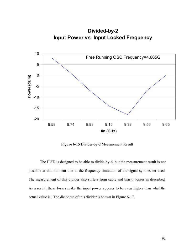
92
Divided-by-2Input Power vs Input Locked Frequency
-20
-15
-10
-5
0
5
10
8.58 8.74 8.88 9.15 9.38 9.56 9.65
fin (GHz)
Pow
er (d
Bm
)
Free Running OSC Frequency=4.665G
Figure 6-15 Divider-by-2 Measurement Result
The ILFD is designed to be able to divide-by-6, but the measurement result is not
possible at this moment due to the frequency limitation of the signal synthesizer used.
The measurement of this divider also suffers from cable and bias-T losses as described.
As a result, these losses make the input power appears to be even higher than what the
actual value is. The die photo of this divider is shown in Figure 6-17.

93
Divided-by-4Input Power Vs Input Locked Frequency
0
2
4
6
8
10
18.54 18.57 18.65 18.73 18.75
fin (GHz)
Pow
er (d
Bm
)
Free Running OSC Frequency=4.665G
Figure 6-16 Divider-by-4 Measurement Result
Figure 6-17 Die photo of ILFD

94
6.8 CMOS Injection-locked Frequency Divider
A second ILFD is designed in a commercial 0.13µm CMOS technology. The
output tank frequency is tuned to 30GHz and this divider in simulation is operational up
to 60GHz. The results are summarized in Table 6-2. However due to a PMOS current
source/transconductor stage is used, large input injection power is required. Furthermore,
the PMOS transistors do not have accurate model at 60GHz. In addition, the layout
requires a third RF probe, which is unavailable at this moment. As a result, this design
still requires more adjustments.
Vdd 1.2V Idd 8.5mA Free-running oscillation frequency
30GHz
Lock Range 6.7% (58G-62GHz) Table 6-2 Simulation results of a CMOS ILFD
Figure 6-18 Layout of a 60GHz COMS ILFD
95
References
[1] Behzad Razavi, RF Microelectronics, Prentice Hall PTR; 1st edition
[2] Hui Wu and Ali Hajimiri, “A 19GHz 0.5mW 0.35µm CMOS Frequency Divider with Shunt-Peaking
Locking-Range Enhancement and Slides,” Solid-State Circuits Conference, 2001
[3] Hamid R. Rategh, Dirad Samavati and Thomas Lee, “A CMOS Frequency Synthesizer with an
Injected-Locked Frequency Divider for a 5-GHz Wireless LAN Receiver,” VLSI Circuits, 1999.
[4] David Pozar, Microwave Engineering, John Wiley & Sons; 2nd Edition
[5] Robert Meyer, EE242 Lecture Notes
[6] Behzad Razavi, Design of Analog CMOS Integrated Circuits, McGraw-Hill Science/Engineering/Math
[7] H.R Rategh and T.H Lee, “Superharmonic injection-locked frequency dividers,” IEEE JSSC, vol. 34,
pp. 813-821, June 1999.
[8] O.Llopis, H.Amine, M.Gayral, J.Graffeuil, J.f. Sautereau, “Analytical Model of Noise in an Analog
frequency Divider,” Microwave Symposium Digest, 1993.
[9] William Egan, “Modeling Phase Noise in Frequency Divider, Ultrasonics, Ferroelectrics and Frequency
Control,” IEEE Transactions on , Volume: 37 Issue: 4 , July 1990
[10] D.Y.C. Lie, X. Yuan, L.E. Larson, T. Robinson, A. Senior, J. Mecke and X. Wang, “Phase Noise
Analysis of Fully-Integrated Digitally-Tuned Wideband Si/SiGe BiCMOS VCOs,” Bipolar/BiCMOS
Circuits and Technology Meeting, 2002
[11] Hao Li, and Hans-Martin Rein, “Millimeter-Wave VCOs with Tuning Range and Low Phase Noise,
Fully Integrated in a SiGe Bipolar Production Technology,” Solid-State Circuits, IEEE Journal of ,
Volume: 38 Issue: 2 , Feb. 2003
[12] J.Mullrich, W.Klein, R.Khlifi and H-M Rein, “SiGe Regenerative Frequency Divider Operating up to
63GHz,” Electronics Letters , Volume: 35 Issue: 20 , 30 Sept. 1999
[13] H.Knapp, T.Meister, M.Wurzer, D.Zosehg, K.Aufinger, L. Treitinger, “A 79GHz Dynamic Frequency
Divider in SiGe Bipolar Technology,” Solid-State Circuits Conference, 2000
[14] R.H. Derksen and H-M Rein, “7.3GHz Dynamic Frequency Dividers Monolithically Integrated in a
Standard Bipolar Technology,” Microwave Theory and Techniques, IEEE Transactions on , Volume: 36
Issue: 3 , March 1988
96
Chapter 7
Conclusions
In this work, the design technique of a 30GHz LNA is discussed. The LNA
achieves all the important requirements such as high gain, wideband, adequate
input/output match and low power dissipation despite multi-stage design used. Monte
Carlo simulations have shown excellent performance even with consideration of
component variations and interconnection parasitic.
The designs of two types of dividers are also presented. The static wideband
divider is designed and verified up to 20GHz while dissipating 3mW in the core circuitry.
The injection-locked divider is also designed and verified to be operational for the divide-
by-2 (9.4G to 4.8G) and divide-by-4 (18.8G to 4.8G). The ILFD dissipates only 1.7mW,
about half of the static divider. Both dividers are operational up to 30GHz according to
simulation results and will be verified from actual wafer measurement once the necessary
test equipments are available.
However there are a lot of areas for improvement. The LNA is targeted at 30GHz
as part of a 30GHz front-end receiver chain. The future work is definitely to verify its
performance. After that, the center frequency of the LNA should be scaled up to the
desired carrier frequency of 60GHz. Even though full chip metal layer EM simulation is
carefully performed and analyzed to account for inductive coupling, problems could still

97
arise due to unaccounted elements such as substrate network coupling and inaccurate
transistor models.
In addition, CMOS LNA implementation should be considered. Since baseband
circuitry requires digital processing, it would be desirable to implement both the analog
front end and digital circuits on the same substrate, reducing the cost of the entire system.
With CMOS technology, new challenges will arise and different design methodology
may be required.
The frequency scaling also applies to the dividers. These circuits should also be
considered in commercial low-cost CMOS processes as well. Furthermore, these
dividers may possibly be implemented as a part of the frequency synthesizer which is an
essential component in any frequency or phase modulation wireless system.
Although these transceiver building blocks are not the versions that will be used
in the final system, they serve as a good starting point for future 60GHz WLAN
microwave designs in commercial SiGe and CMOS processes. These circuits provide
useful results and potential shortcomings to design microwave circuitry utilizing these
standard processes.