Embed Size (px)
Citation preview

Robotics: Science and Systems 2005Cambridge, MA, USA, June 8-11, 2005
1
Abstract— The contact phase of an assembly task involving
micro and nano objects is complicated by the presence of surface and intermolecular forces such as electrostatic, surface-tension and Van der Waals forces. Assembly strategies must account for the presence of these forces in order to guarantee successful repeatable micro and nanoassemblies with high precision. A detailed model for this electrostatic interaction is developed and analyzed. Based on the results of this analysis, dielectrophoretic assembly principles of MEMS/NEMS devices are proposed and experimentally verified with microtweezers for micro Ni parts and with nanoelectrodes fabricated with electron-beam lithography for carbon nanotube assembly. The successful manipulation and assembly of single carbon nanotubes (CNTs) using dielectrophoretic forces produced by nanoelectrodes will lead to a higher integration of CNTs into both nanoelectronics and NEMS.
Index Terms— Microassembly, nanoassembly, MEMS, NEMS, dielectrophoresis, carbon nanotubes
I. INTRODUCTION HE scaling of micro/nanoparts leads to the dominance of surface and intermolecular forces such as electrostatic, van
der Waals, and surface tension forces. This dominance also results in complications in part handling and micro/nanomanipulation for creating component assemblies. Interactive forces are highly dependent on the operating environment and material properties of the contacting surfaces [1, 2, 3] making a priori estimation of these forces difficult. As a result, assembly strategies must be developed that account for interactive forces during all contact phases of the assembly. This requires a model of the interactive forces for understanding their influence on the assembly configuration.
A. Subramanian is with the Institute of Robotics and Intelligent Systems (IRIS) at the Swiss Federal Institute of Technology (ETH), Zürich (telephone: +41 44 632 68 64, email: [email protected]).
B. Vikramaditya is with Seagate Technology, Bloomington, MN 55435 (telephone: +1-952-402-8521, email: Barmeshwar.Vikramaditya@seagate. com).
L.X. Dong is with IRIS at ETH, Zürich (telephone: +41 44 632 25 39, email: [email protected]).
D. Bell is with IRIS at ETH, Zürich (telephone: +41 44 632 68 64, email: [email protected]).
B.J. Nelson heads IRIS at ETH, Zürich (telephone: +41 44 632 55 29, email: [email protected]).
As pointed out by Feddema et al. [4] the geometric constraints of the assembly planner and the free space path planning of the motion planner remain unchanged in the micro-domain. However, fine motion planning and precision motion at micro and nanoscales differ, particularly where contact is involved. Reversing the motion used to pick up a part will generally not release it. The specification of goals is different and must be correctly modeled.
Another important difference in manipulation at micro and nanoscales is that the attractive nature of interactive forces can also be exploited to allow for self-assembly. By achieving a suitable geometric preconfiguration, interactive forces can be leveraged to allow components to self-assemble and achieve the desired final configuration. The short range of the interactive forces allows for the use of existing global path planning techniques for coarse positioning, but new path planning methods are needed for fine positioning. By understanding the qualitative and quantitative nature of these forces, assembly strategies can be developed that leverage the interactions to enable robust assembly.
One of the forces of particular interest for MEMS and NEMS assembly is due to the phenomenon of dielectrophoresis (DEP). This phenomenon describes how certain uncharged materials placed in an electric field experience a net force and torque resulting in motion, which can be used for the manipulation of small parts. Assembly with dielectrophoresis is a potentially important bottom-up technology for the construction of MEMS and NEMS with as-fabricated and/or as-grown building blocks.
Carbon nanotubes (CNTs) are one of the most important nanomaterials for the construction of nanoelectronic devices and NEMS because of their exceptional properties and special structure. For NEMS, some of the most important characteristics of nanotubes include their nanometer diameter, large aspect ratio (10-1000), TPa scale Young’s modulus, excellent elasticity, ultra-small interlayer friction, sensitivity of conductance to various physical or chemical changes, and charge-induced bond-length change. Devices based on individual single- or multiwalled carbon nanotubes (SWNTs or MWNTs) are of increasing interest, indicating that capabilities for incorporating individual CNTs at specific locations on a device must be developed.
Random spreading [5], direct growth [6], self-assembly [7], and nanomanipulation [ 8 ] have been demonstrated for
Micro and Nanorobotic Assembly Using Dielectrophoresis
Arunkumar Subramanian, Barmeshwar Vikramaditya, Lixin Dong, Dominik Bell, and Bradley J. Nelson
T
positioning nanotubes on electrodes for the construction of these devices. The direct growth method has been used for the integration of CNTs on electrodes, e.g, thermal chemical vapor deposition (CVD) has been used to grow a single SWNT across a pair of electrodes with a high yield [9]. Growth was achieved, however, at a temperature of 900°C, which may be prohibitively high for making fully integrated devices. Furthermore, SWNT spacing of 500 µm or greater was necessary to avoid growth in unwanted directions. A chemical patterning method has been demonstrated to deposit discrete SWNTs by electrostatic interaction [ 10 , 11 , 12 ]. The processing steps, however, are sensitive to the chemical functionalization of both the SWNT and the substrate, which could be an issue both in processing and performance. Assembly with dielectrophoresis is a potentially important bottom-up technology for the mass production of NEMS with as-grown carbon nanotubes. There have been various approaches to exploiting dielectrophoretic assembly of nanoscale and microscale components. [13, 14, 15, 16]. An electric field method that mixes alternating current (AC) and direct current (DC) electric fields for achieving deposition of individual components in an array has been used recently to assemble discrete MWNTs across 100 opposing electrode pairs. This method lends itself to mass production [ 17 ]. The composite electric field with a particular ratio of the magnitudes of AC:DC electric fields was used to place a single MWNT spanning a pair of opposing electrodes separated by a gap. However, the electrodes themselves are still large, typically 4 µm gap distance and 300 µm width. To investigate the physical limitations of integration, we demonstrate the assembly of individual MWNTs using DEP forces as above, but with much smaller electrodes fabricated using electron-beam lithography.
This paper considers the use of electrostatic forces for self-assembly strategies of micro- and nanostructures. Previous approaches to stochastic self-assembly of MEMS devices are first described. Lessons from these approaches and an understanding of the nature of interactive forces are then used to develop deterministic assembly plans motivated by self-assembly principles. A pick-and-place task using micro tweezers is modeled for this purpose. Based on an understanding of the part-gripper interactions, assembly principles are devised for manipulating parts of varying geometric and material properties using electrostatic part interactions. Applying this same approach at the nanoscale provides a way to integrate as-grown carbon nanotubes into NEMS using nanoelectrodes.
II. APPROACH
A. Electrostatic Part Interactions In a uniform electric field there is no net force on a dipole,
however if the dipole moment is not aligned with the field, E, then there is an alignment torque per unit volume, T, given by
EPT ×= (1) where P is the polarization of the medium. For a linear dielec-tric this torque is zero because the polarization is induced by the field and hence aligned with it. In a nonuniform field the object experiences a net force in addition. The net force per unit volume, f, on the object given by
( )EPf •∇= (2) and if there is a net charge on the material then the total force per unit volume is
( ) EEPf fρ+•∇= (3)
where fρ is the free charge density on the medium. These
equations can be used to determine the force acting on a polarized medium in an electric field. As an example, the axial force on a permanently polarized medium and a linear polarized medium in a gripper configuration are given as [18]
0
20
0 εsdPVdPf x += (4)
and ( )
sdVf x
20εε −
= (5)
respectively, where P0 is the polarization of the permanently polarized medium, V is the applied potential difference, ε is the relative permittivity of the linearly polarized medium and d is the depth of the plates.
As a result, a permanently polarized medium can be either pulled in or pushed out of the gripper depending on the polarity and magnitude of the applied voltage, whereas, the linearly polarized medium is always pulled into the gripper irrespective of the voltage polarity. Most microfabricated devices are linearly polarized and as a result can be pulled into a parallel-jaw gripper by applying a potential across the plates. The pull-in force can be leveraged to align the parts within the gripper by shape forming the gripper to enable self-alignment of the parts. In addition, this force can also be used to ensure guaranteed release of parts by maintaining a potential differ-ence between the gripper and the placement substrate.
The behavior of objects with critical dimensions less than a millimeter in a dielectric media subjected to an electric field can be determined by the dielectrophoresis approximation [19]. Dielectrophoresis is the resultant of forces exerted upon noninteracting objects by (1) an externally imposed nonuniform electric field and (2) the mutual attractive or repulsive force between two or more closely spaced objects due to moments induced by an external electric field.
According to Jones, the time dependent force, )(tFDEP , and
torque, )(tT e , on a particle in an electric field, )(tE can be expressed in terms of the “effective moment” identified by the solutions of the induced electrostatic field due to the particle in an electric field and can be expressed as
EtptF efffDEP ))(()( •∇= (6)
)()()( tEtptT effe ×= (7)
where effp is a charge free point dipole which when immersed
in the same media as the original particle produces the same dielectric field. As an example, for a homogenous dielectric sphere with permittivity 2ε
in a media of permittivity 1ε
sub-
ject to a uniform electric field of intensity 0E , the effective dipole moment is
03
14 EKrpeff πε= (8)
where K is the Claussius-Mossotti function, which provides a measure of the strength of the effective polarization as a func-tion of the surrounding dielectric media with dielectric constant
2ε and
12
1221 2),(
εεεεεε
+−
=K (9)
This formulation is valid for a conducting sphere placed in a conductive media subject to a uniform electric field. In this case
the permittivities, 2,1ε , are replaced by conductivities, 2,1σ , and the Claussius-Mossotti function is given as
12
1221 2),(
σσσσσσ
+−
=K (10)
For the limiting case of a perfectly conductive sphere the effective dielectric moment is given as 0
310 4 Erp πε= .
An application of (6) for the case where a lossless spherical particle of permittivity ε2 is placed in a lossless dielectric medium of permittivity ε1 and subjected to a slightly nonuni-form electric field E0 , results in a net force on the particle given by
2021
31 ),(2 EKrFDEP ∇= εεπε (11)
For significantly nonuniform electric fields, higher order corrections are needed and multi-pole expansions are necessary. Based on these results the following conclusions can be made:
• The force experienced is proportional to the volume of the object.
• The force is proportional to the permittivity of the sus-pension media ε1.
• The force is directed along the gradient of electric field intensity, 2
0E∇ , which is not necessarily aligned with the applied electric field.
• The DEP force depends on the magnitude and sign of the Claussius-Mossotti function, K. For a positive K, objects are attracted to electric field intensity maxima and repelled from minima which is known as positive DEP. For a negative K, objects are attracted to electric field intensity minima and repelled from maxima which is known as negative DEP.
In addition to material property, shape anisotropy can also be exploited to generate both a DEP force and a torque. This effect can be exploited to orient and manipulate objects subject to electric and magnetic fields.
An ellipsoidal geometry is used to illustrate this feature. An isotropic ellipsoid of permittivityε2 with semi-axes a, b and c in a medium of permittivity ε1 subject to a uniform electric field
kEjEiEE zyx ++=0 which is not necessarily aligned with
any of the axes of the ellipsoid is subject to an alignment torque kTjTiTT zyx
e ++= with,
Fig. 1. Force on polarized medium in a gripper.
Fig. 3. Behavior of a rotated part during pickup using a parallel-jaw gripper.
Fig. 2. Simulation results for the release sequence of a Ni part.
⎥⎥⎦
⎤
⎢⎢⎣
⎡⎟⎟⎠
⎞⎜⎜⎝
⎛ −+
⎥⎥⎦
⎤
⎢⎢⎣
⎡⎟⎟⎠
⎞⎜⎜⎝
⎛ −+
−−=
zy
zyyxx
LL
EELLabcT
1
12
1
121
212
113
)()(4
εεε
εεεε
εεπ (12)
where zyxL ,, are the depolarization factors computed through
elliptical integrals [19]. The depolarization factors are related with 10 ,, ≤≤ zyxL and 1=++ zyx LLL . In addition,
01 ,,1
12 >⎟⎟⎠
⎞⎜⎜⎝
⎛ ++ zyxL
εεε . Similar expressions may be obtained
for the other components of the alignment torque. Qualitatively, zyyzx EELLT )( −∝ , xzzxy EELLT )( −∝ and
yxxyz EELLT )( −∝ . Simplifications can be obtained for pro-
late (cigar shaped) and oblate (lenticular) spheroids. The DEP force experienced by the ellipsoid in the presence
of a slightly nonuniform electric field is given by [19]
0
1
12
12 ...1
3)(4 E
xL
EabcF
y
xDEP
⎥⎥⎥⎥⎥
⎦
⎤
⎢⎢⎢⎢⎢
⎣
⎡
+∂∂
⎟⎟⎠
⎞⎜⎜⎝
⎛ −+
−=
εεε
εεπ (13)
The qualitative behavior of shape anisotropy based DEP force is similar to that of a spherical particle. Shape anisotropy also results in a torque in magnetic fields and magnetophoretic forces in a nonuniform magnetic field.
For more general part geometries a finite-element based simulation is necessary in order to estimate the interaction between contacting elements during the course of a microassembly task. Modeling and understanding the interactive forces yields feasible assembly plans. In addition, grippers can be designed to exploit the interactive forces to enable guaranteed pickup and release of parts. Substrate surfaces can be temporarily coated with conductive material to leverage the interactive forces to enable repeatable deterministic assembly. The formulations developed in this
section serve as guidelines for the design of dry self-assembling microstructures.
III. MOTIVATED BY SELF-ASSEMBLY The effects of electrostatic forces were observed during the
course of visually servoed microassembly tasks. This was unexpected as most of the guidelines for selection of gripper materials suggested by Fearing [2]. The gripper fingers were composed of a highly conductive Ni-Ti alloy that had been fabricated using electric-discharge machining which resulted in a rough contacting surface while hardening the surface as well. The guideline requiring a minimization of contact potential between the gripper and the objects could not be adhered to due to the requirements of the task. The part being manipulated was a LIGA microfabricated 150x100x100 µm cuboid made of Ni. The part was picked-and-placed on a dielectric Si wafer. The Si wafer had earlier been processed using LPCVD (low-pressure chemical vapor deposition) and sputtering in order to create alignment features on it for visual servoing resulting in nearly complete oxidation. This prevented the part from being grounded with respect to the gripper in addition to the geometric constraints due to the small size of the gripper fingers.
The grippers fingers were actuated by a piezoelectric linear actuator which was driven by a time varying 200 Vp-p supply. In addition, the gripper fingers rubbed against a metallic barrel during the course of opening and closing. Both these sources could be responsible for distributing surface charge on the gripper fingers. Since the part was being picked-and-placed from a dielectric surface, there was a possibility of contact electrification of the substrate which would then retain the charge.
Surface charge density is limited to 3x10⁻⁵ C/m2 according to Fearing [2]. Assuming a charge density of 2x10⁵ C/m2, the electrostatic pressure on the cuboid due to the charge distribution would be about 22 Pa. The nickel cuboid with density 8.9 g/cm3 weighs approximately 1.62x10⁻⁷ N, and the resulting electrostatic force is approximately 2.91x10⁻⁷ N, which is sufficient to manipulate the part. This suggests that electrostatic forces are sufficient to overcome inertial forces and should be able to cause motion of the part as was observed.
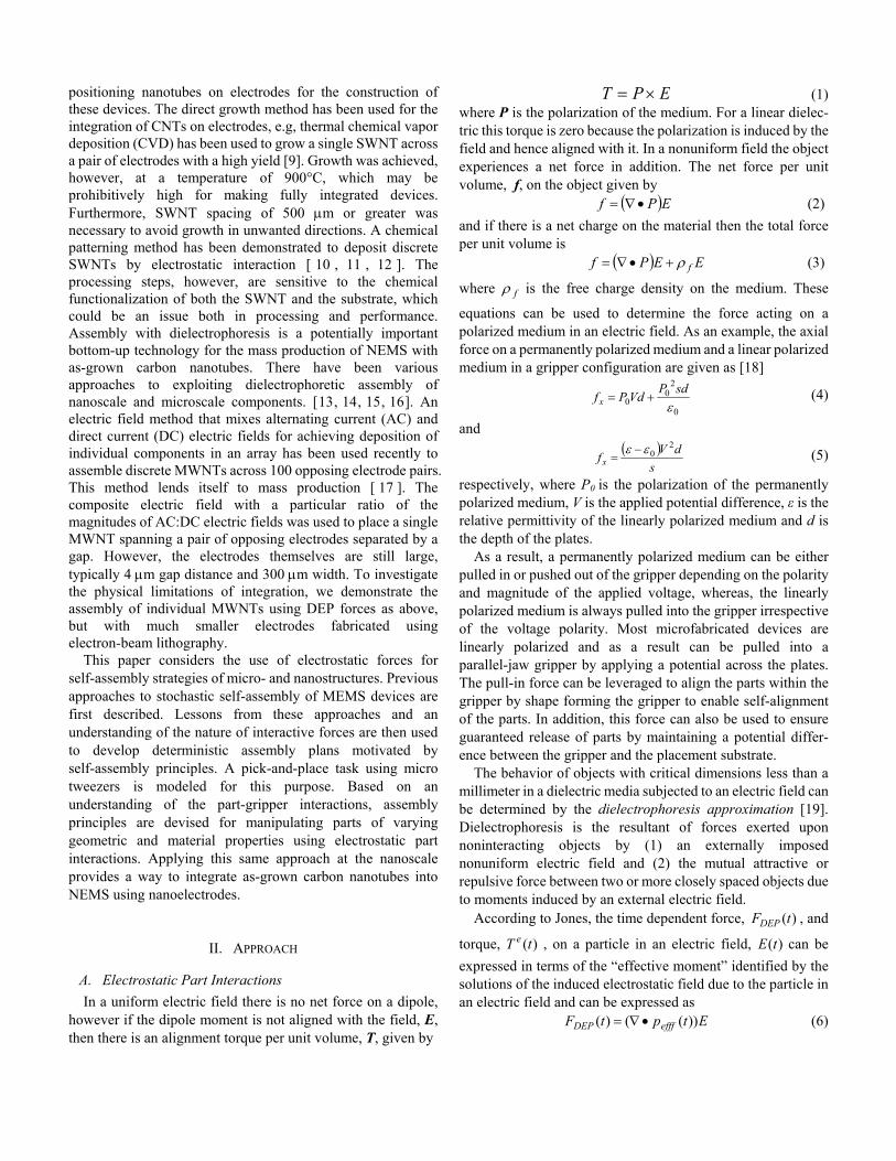
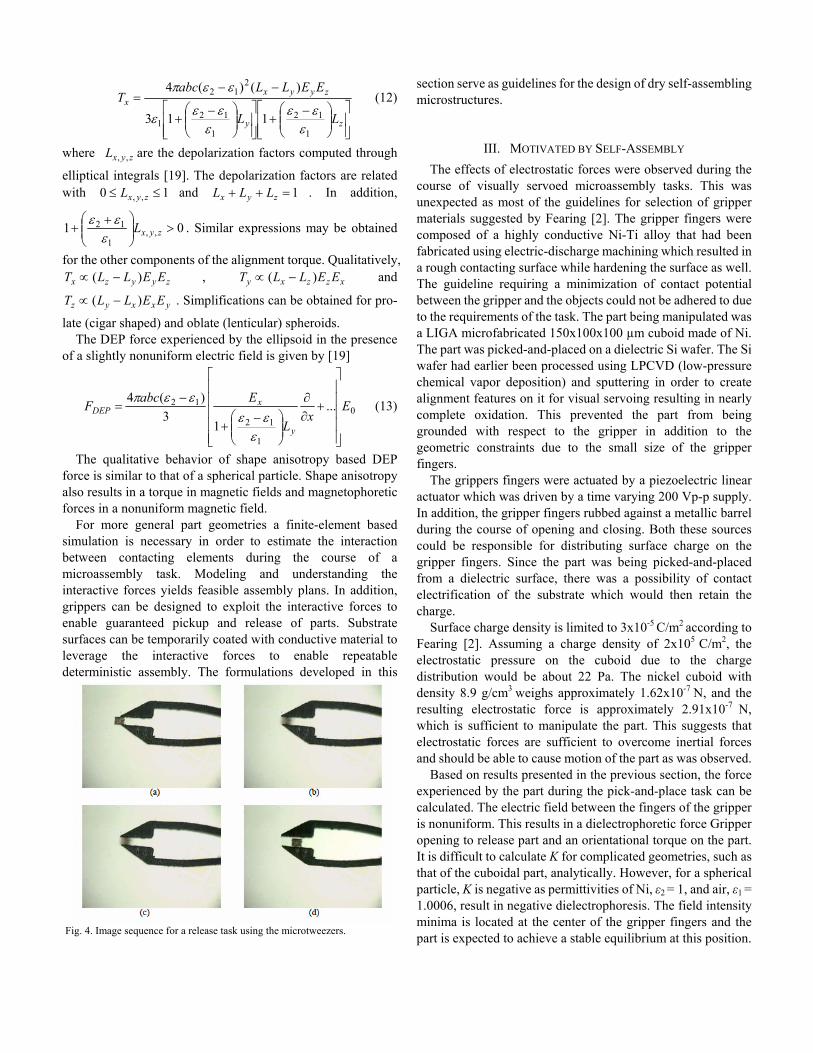
Based on results presented in the previous section, the force experienced by the part during the pick-and-place task can be calculated. The electric field between the fingers of the gripper is nonuniform. This results in a dielectrophoretic force Gripper opening to release part and an orientational torque on the part. It is difficult to calculate K for complicated geometries, such as that of the cuboidal part, analytically. However, for a spherical particle, K is negative as permittivities of Ni, ε2 = 1, and air, ε1 = 1.0006, result in negative dielectrophoresis. The field intensity minima is located at the center of the gripper fingers and the part is expected to achieve a stable equilibrium at this position. Fig. 4. Image sequence for a release task using the microtweezers.

In addition, the part has shape anisotropy which results in an orientational torque.
Finite element analysis using Ansoft Maxwell 2D Field Simulator was conducted for different stages of the pick-and-place task using a simplified geometry of the gripper. The gripper fingers (Ni-Ti alloy) were assumed to be at a potential of 200V, with a linearly polarized Ni part between the gripper fingers. The equipotential field lines are plotted as an arrow plot superposed on the figure. Results are shown in Fig. 2. As expected, the Ni part moves towards the minima of the electric field intensity. When the same simulation was run with a Si part ( ε2 = 11.9 ), positive DEP was observed, as expected by the positive Claussius-Mossotti function for a similar part composed of Si. The orientational torque for the Ni part tends to align the longer side parallel to the gripper jaws, which is used to guarantee the orientation of pick-and-place operations.
Experimental results correlate closely with the simulation results. The part clearly moves to the minima of electric field intensity upon release. This movement can be compensated for in the path plan. Alternatively, by picking up the part already centered within the jaws of the gripper, final position and orientation accuracy can be guaranteed.
The corresponding captured video sequence is shown in Fig. 4. The experiment was very repeatable and the same behavior was observed for all Ni parts that were manipulated. However, the repeatability for Si parts was not as good. This was in part due to the fabrication process of the Si parts which had been diced after several microfabrication steps. The orientation torque effects were also observed for some Si parts that were dimensionally equivalent to the simulated part.
IV. NANOASSEMBLY OF CARBON NANOTUBES ONTO NANOELECTRODES
In this section, we extend the previous discussion into the nanoscale and demonstrate the suitability of electric field directed assembly techniques to precisely place multi-walled carbon nanotubes from a suspension onto regions between gold nanoelectrodes patterned by electron beam lithography. Nanoassembly results are presented for electrophoresis driven by both pure AC and AC-DC composite fields. The influence of factors such as MWNT concentration in suspension, deposition time and AC-DC components of the electric field are discussed.
A. Theory Just as in the case of neutrally charged micron sized objects,
when a suspension containing multi-walled carbon nanotubes is placed in an AC electric field generated by nanoelectrodes, a dipole moment is induced in the nanotubes, and they experience a dielectrophoretic force that is given by (6). For long cylindrical objects such as nanotubes, this equation, which is a more general form of (11), may be written as [20]
20212 )},(Re{ EKFDEP ∇Γ= εεε (14)
where Г is a factor depending on geometry, ε2 represents the complex permittivity of the suspension medium, K(ε1,ε2) represents the complex polarization factor (for spherical objects this is know as the Claussius-Mossotti function) and E0 denotes the applied non-uniform electric field. For a nanotube of length l and radius r, the geometric factor Г is given by
6
2lrπ=Γ (15)
and the complex polarization factor is given by
2
2121 ),(
εεεεε −
=K (16)
where ε1 represents the complex permittivity of the nanotube. This dielectrophoretic force causes the nanotubes to align
themselves along the electric field and move towards either the electric field minima or maxima depending on the relative permittivity of the nanotubes with respect to the suspending medium.
Though the AC dielectrophoresis technique can selectively assemble nanotubes from a solution without impurities and also orient them along the field lines, it is difficult to assemble individual nanotubes with this method. A composite electrophoretic technique has been employed [17] to deposit individual nanotubes between microelectrodes. Here it is suggested that the vortex flows generated by the DC component of the electric field after the deposition of a multi-walled nanotube inhibit further deposition of nanotubes in its vicinity. In this effort, we have demonstrated this coupled field directed assembly in the nanoscale which is an important step towards realizing NEMS and other nanodevices.
B. Electrode Fabrication and Nanoassembly The steps involved in the electrode nanofabrication process
and the nanoassembly of multiwalled nanotubes is shown in Fig 5. First, a 100 nm layer of silicon dioxide was deposited on a silicon substrate for isolation. This was followed by the definition of 45 nm thick gold electrodes. The electrodes were defined by electron beam lithography and lift-off. A 15 nm layer of chromium was used to improve the adhesion of gold to the oxide.
Next, multi-walled nanotubes were deposited onto the electrodes by AC or coupled AC – DC electrophoresis. For this step, multi-walled nanotubes prepared by CVD were obtained from Nanolab Inc., USA and sonicated in Triton X – 100. The nanotubes in the suspension were 20 – 40 nm in diameter and about 5 – 20 µm long. A droplet of this suspension was placed on the chip and the electric field was applied with a high frequency function generator. Experiments were carried out with purely AC fields at 5 – 12 MHz as well as with coupled AC – DC fields. At the end of 30 – 60 sec, the droplet was blown off and the field was removed.
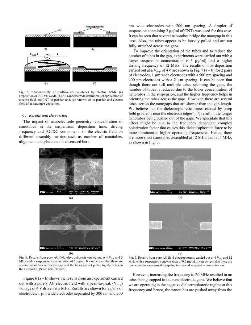
Fig. 5. Nanoassembly of multiwalled nanotubes by electric fields. (a) Deposition of PECVD oxide, (b) Au nanoelectrode definition, (c) application of electric field and CNT suspension and, (d) removal of suspension and electric field after nanotube deposition.
C. Results and Discussion The impact of nanoelectrode geometry, concentration of
nanotubes in the suspension, deposition time, driving frequency and AC/DC components of the electric field on different assembly metrics such as number of nanotubes, alignment and placement is discussed here.
(a)
(b)
Fig. 6. Results from pure AC field electrophoresis carried out at 4 Vp–p and 5 MHz with a suspension concentration of 2 µg/ml. It can be seen that there are several nanotubes across the gap, and the tubes are not pulled tightly between the electrodes. (Scale bars: 300nm)
Figure 6 (a – b) shows the results from an experiment carried
out with a purely AC electric field with a peak-to-peak (Vp– p) voltage of 4 V driven at 5 MHz. Results are shown for 2 pairs of electrodes, 1 µm wide electrodes separated by 300 nm and 200
nm wide electrodes with 200 nm spacing. A droplet of suspension containing 2 µg/ml of CNTs was used for this case. It can be seen that several nanotubes bridge the nanogap in this case. Also, the tubes appear to be loosely pulled and are not fully stretched across the gaps.
To improve the orientation of the tubes and to reduce the number of tubes in the gap, experiments were carried out with a lower suspension concentration (0.5 µg/ml) and a higher driving frequency of 12 MHz. The results of this deposition carried out at a Vp–p of 4V are shown in Fig. 7 (a – b) for 2 pairs of electrodes, 1 µm wide electrodes with a 500 nm spacing and 400 nm electrodes with a 2 µm spacing. It can be seen that though there are still multiple tubes spanning the gaps, the number of tubes is reduced due to the lower concentration of nanotubes in the suspension, and the higher frequency helps in orienting the tubes across the gaps. However, there are several tubes across the nanogaps that are shorter than the gap length. We believe that the dielectrophoretic forces caused by steep field gradients near the electrode edges [17] result in the longer nanotubes being pushed out of the gaps. We speculate that this effect might be due to the frequency dependant complex polarization factor that causes this dielectrophoretic force to be more dominant at higher operating frequencies. Hence, there are more short nanotubes assembled at 12 MHz than at 5 MHz, as shown in Fig. 7.
(a)
(b)
Fig. 7. Results from pure AC field electrophoresis carried out at 4 Vp–p and 12 MHz with a suspension concentration of 0.5 µg/ml. It can be seen that there are fewer nanotubes across the gap due to reduced suspension concentration.
However, increasing the frequency to 20 MHz resulted in no tubes being trapped in the nanoelectrode gaps. We believe that we are operating in the negative dielectrophoretic regime at this frequency and hence, the nanotubes are pushed away from the

electrodes towards the electric field minima. The results from this experiment carried out at a Vp–p of 10V and a suspension concentration of 0.5 µg/ml is shown for an array of 100 nm wide nanoelectrodes in Fig. 8 (a). It can be seen that even at a voltage that is much higher than the previous cases, there is no deposition of tubes and this confirms that we are operating above the crossover frequency for this nanoparticle – medium combination.
Also, the impact of the electrophoresis time on the number of tubes is shown in Fig. 8 (b). Here the assembly parameters are identical to that of the previous case shown in Fig. 7 (a), except for a reduced deposition time of 30 sec. It can be seen that the number of nanotubes spanning the gap is much lower, as is to be expected.
(a)
(b)
Fig. 8. (a) Results from pure AC field electrophoresis carried out at 10 Vp–p and 20 MHz with a suspension concentration of 0.5 µg/ml. It can be seen that there are no nanotubes across the gap due to negative dielectrophoresis. (b) Results from pure AC field electrophoresis carried out at 4 Vp–p and 12 MHz with a suspension concentration of 0.5 µg/ml. It can be seen that there are fewer nanotubes across the gap due to a reduced electrophoresis time of 30 sec.
Next, a composite electric field comprising an AC component and a DC bias was applied across the nanoelectrodes. Previously, this was experimentally shown at the microscale in [21] and the DC bias was believed to create vortex flows in the vicinity of an assembled nanotube that prevent further nanotube deposition. We have shown this principle to work in the nanoscale across nanoelectrode arrays with an Edc / Eac ratio of 0.7. The AC field was applied at a frequency of 12 MHz and the suspension concentration was 0.5 µg/ml. Since the DC field delays the deposition of the nanotubes, the electrophoresis time was increased to 240 sec. Also, to further delay the deposition of additional nanotubes
once the first tubes are attracted to the nanoelectrodes, a large impedance was introduced into the circuit in series with the nanoelectrodes. This was implemented by leaving one of the 2 nanoelectrodes floating and applying the bias between the other nanoelectrode and a bonding pad located on the chip at about 500 µm from the nano-electrode pair, as schematically illustrated in Fig. 9.
Fig. 9. Coupled field dielectrophoresis with a floating nanoelectrode
(a)
(b)
Fig. 10. Results from composite AC – DC field electrophoresis carried out at 4 Vp – p, 1 Vdc bias and 12 MHz, with a suspension concentration of 0.5 µg/ml. (a) It can be seen that individual nanotubes bridge the gap with increased inter-tube spacing. (b) A higher magnification image showing the individual tubes.
The results of coupled field dielectrophoretic nanoassembly are shown in Fig. 10 (a – b). It can be seen that the coupled field increases the spacing between nanotubes and helps in obtaining individual MWNTs across the nanoelectrode gaps. This is shown for 5 µm wide electrodes with a 300 nm gap.
Another parameter that improved the placement accuracy of individual nanotubes was electrode geometry. It was observed that having arrays of sharp nanoelectrode tips across large electrodes provides for local maxima in the electric fields and the nanotubes preferentially align in these regions across these nanoelectrode tips. This effect was investigated with 5 µm wide electrodes having a 2 µm spacing. A 100 nm nanoelectrode
~
Bias Electrodes
Floating Electrodes
~
Bias Electrodes
Floating Electrodes
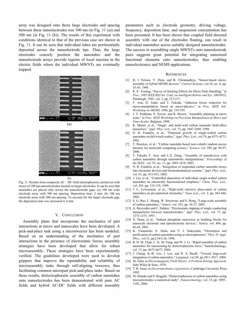
array was designed onto these large electrodes and spacing between these nanoelectrodes was 300 nm (in Fig. 11 (a)) and 500 nm (in Fig. 11 (b)). The results of this experiment with conditions identical to that of the previous case are shown in Fig. 11. It can be seen that individual tubes are preferentially deposited across the nanoelectrode tips. Thus, the large electrodes coarsely position the nanotubes and the nanoelectrode arrays provide regions of local maxima in the electric fields where the individual MWNTs are eventually trapped.
(a)
(b)
Fig. 11. Results from composite AC – DC field electrophoresis carried out with arrays of 100 nm nanoelectrodes located on larger electrodes. It can be seen that nanotubes are placed only across the nanoelectrode gaps. (a) 100 nm wide electrode array with 300 nm spacing. Deposition time: 2 min. (b) 100 nm electrode array with 500 nm spacing. To account for the larger electrode gap, the deposition time was increased to 4 min.
V. CONCLUSION Assembly plans that incorporate the mechanics of part
interactions at micro and nanoscales have been developed. A pick-and-place task using a microtweezer has been modeled. Based on an understanding of the mechanics of part interactions in the presence of electrostatic forces, assembly strategies have been developed that allow for robust microassembly. These strategies have been experimentally verified. The guidelines developed were used to develop grippers that improve the repeatability and reliability of microassembly tasks through self-aligning tweezers, thus facilitating common micropart pick-and-place tasks. Based on these results, dielectrophoretic assembly of carbon nanotubes onto nanoelectrodes has been demonstrated with pure AC fields and hybrid AC-DC fields with different assembly
parameters such as electrode geometry, driving voltage, frequency, deposition time, and suspension concentration has been presented. It has been shown that coupled field directed assembly with one of the electrodes floating, can result in individual nanotubes across suitably designed nanoelectrodes. The success in assembling single MWNTs onto nanoelectrode pairs suggests great potential for integrating nanosized functional elements onto nanoelectrodes, thus enabling nanoelectronics and NEMS applications.
REFERENCES [1] B. J. Nelson, Y. Zhou, and B. Vikramaditya, “Sensor-based micro-
assembly of hybrid MEMS devices,” Control Systems, vol.18, no. 6, pp. 35-45, 1998.
[2] R. S. Fearing, “Survey of Sticking Effects for Micro Parts Handling,” in Proc. 1995 IEEE/RSJ Int. Conf. on Intelligent Robots and Sys. (IROS95), Pittsburgh, 1995, vol. 2, pp. 212-217.
[3] F. Arai, D. Ando, and T. Fukuda, “Adhesion forces reduction for micro-manipulation based on micro-physics,” in Proc. IEEE Intl. Workshop on MEMS, 1996, pp. 354-359.
[4] J. T. Feddema, P. Xavier, and R. Brown, “Assembly planning at micro scale,” in Proc. IEEE Workshop on Precision Manipulation at Micro and Nano Scales, Belgium, 1998.
[5] R. Martel, et al., “Single- and multi-wall carbon nanotube field-effect transistors,” Appl. Phys. Lett., vol. 73, pp. 2447-2449, 1998.
[6] N. R. Franklin, et al., “Patterned growth of single-walled carbon nanotubes on full 4-inch wafers,” Appl. Phys. Lett., vol.79, pp.4571-4573, 2001.
[7] T. Rueckes, et al., “Carbon nanotube-based non-volatile random access memory for molecular computing science,” Science, vol. 289, pp. 94-97, 2000.
[8] T. Fukuda, F. Arai, and L.X. Dong, “Assembly of nanodevices with carbon nanotubes through nanorobotic manipulations,” Proceedings of the IEEE, vol. 91, no. 11, pp. 1803-1818, 2003.
[9] N. R. Franklin, et al., “Integration of suspended carbon nanotube arrays into electronic devices and electromechanical systems,” Appl. Phys. Lett., vol. 81, pp. 913-915, 2002.
[10] J. Liu, et al., “Controlled deposition of individual single-walled carbon nanotubes on chemically functionalized templates,” Chem. Phys. Lett., vol. 303, pp. 125-129, 1999.
[11] J. C. Lewenstein, et al., “High-yield selective place-ment of carbon nanotubes on pre-patterned electrodes,” Nano Lett., vol. 2, pp. 443-446, 2002.
[12] S. G. Rao, L. Huang, W. Setyawan, and S. Hong, “Large-scale assembly of carbon nanotubes,” Nature, vol. 425, pp. 36-37, 2003.
[13] A. Bezryadin and C. Dekker, “Electrostatic trapping of single conducting nanoparticles between nanoelectrodes,” Appl. Phys. Lett., vol. 71, pp. 1273-1275, 1997.
[14] X. Duan, et al., “Indium phosphide nanowires as building blocks for nanoscale electronic and optoelectronic devices,” Nature, vol. 409, pp. 66-69, 2001.
[15] K. Yamamoto, S. Akita, and Y. J. Nakayama, “Orientation and purification of carbon nanotubes using ac electrophoresis,” Phys. D: Appl. Phys., vol.31, pp.L34-L36, 1998.
[16] R. H. M. Chan, C. K. M. Fung, and W. J. Li, “Rapid assembly of carbon nanotubes for nanosensing by dielectrophoretic force,” Nanotechnology, vol. 15, pp. S672-S677, 2004.
[17] J. Chung, K.-H. Lee, J. Lee, and R. S. Ruoff, “Toward large-scale integration of carbon nanotubes,” Langmuir, vol.20, pp.3011-3017, 2004.
[18] M. Zahn, in Electromagnetic Field Theory: A Problem Solving Approach, John Wiley & Sons, 1979.
[19] T. B. Jones, in Electromechanics of particles, Cambridge University Press, 1995.
[20] M. Dimaki and P. Boggild, “Dielectrophoresis of carbon nanotubes using microelectrodes: a numerical study”, Nanotechnology, vol. 15, pp. 1095– 1102, 2004.