Embed Size (px)
Citation preview

MGM210L Wireless Gecko Multi-ProtocolLighting Module Data Sheet
The MGM210L is a module designed and built to meet the per-formance, security, and reliability requirements of line-powered,smart LED lighting products.
Based on the EFR32MG21 Gecko SoC, it enables Zigbee®, Thread®, Bluetooth® andmulti-protocol connectivity (Zigbee + Bluetooth) delivering best-in-class RF performance,CA Title 20 energy consumption compliance, future-proof capability for feature and OTAfirmware updates, enhanced security, and a form factor and temperature rating suitedfor enclosed operation in lightbulb housings.
The MGM210L is a complete solution that comes with fully-upgradeable, robust softwarestacks, world-wide regulatory certifications, advanced development and debuggingtools, and support that will simplify and minimize the development cycle and deploymentof your product helping to accelerate its time-to-market.
The MGM210L is targeted for key applications that include:• Smart LED lightbulbs• Connected lighting
KEY FEATURES
• Zigbee, Thread, Bluetooth 5.1 and multi-protocol connectivity
• PCB Trace antenna• +12.5 dBm max TX power• -104 dBm 802.15.4 RX sensitivity• -97 dBm Bluetooth RX sensitivity @ 1
Mbps• 32-bit ARM Cortex-M33 core at 38.4 MHz• 1024/96 kB of flash/RAM memory• Enhanced security features• Optimal set of MCU peripherals• 12 GPIO pins• -40 to (105 or 125)°C• 15.5 mm x 22.5 mm (custom form factor)
Timers and Triggers
32-bit bus
Peripheral Reflex System
Serial Interfaces
I/O Ports Analog I/F
Lowest power mode with peripheral operational:
USART
I2C
External Interrupts
General Purpose I/O
Pin Reset
Pin Wakeup
ADC
Analog Comparator
EM4—Shutoff
Energy Management
Brown-Out Detector
Voltage Regulator
Power-On Reset
SecurityClock Management
HF Crystal Oscillator
LFRC Oscillator
HFRC Oscillator
EM23 HF RC Oscillator
Crypto Acceleration
Secure Debug
Security CoreUltra LF RC Oscillator
Core / Memory
ARM CortexTM M33 processorwith DSP extensions,FPU and TrustZone
ETM Debug Interface RAM Memory LDMA Controller
Flash Program Memory
Real Time Capture Counter
Timer/Counter
Low Energy Timer Watchdog Timer
Protocol Timer
Radio Transceiver
DEMOD
AGC
IFADC
CR
C
BU
FC
MOD
FRC
RA
CFrequency Synth
PGA
EM3—StopEM2—Deep SleepEM1—SleepEM0—Active
True Random Number Generator
Fast StartupRC Oscillator
Back-Up Real Time Counter
RF FrontendI
Q
PA
LNA
PA
Crystal
38.4 MHz
Antenna
PCB Trace Antenna
Matching
LF Crystal Oscillator
silabs.com | Building a more connected world. Rev. 1.0
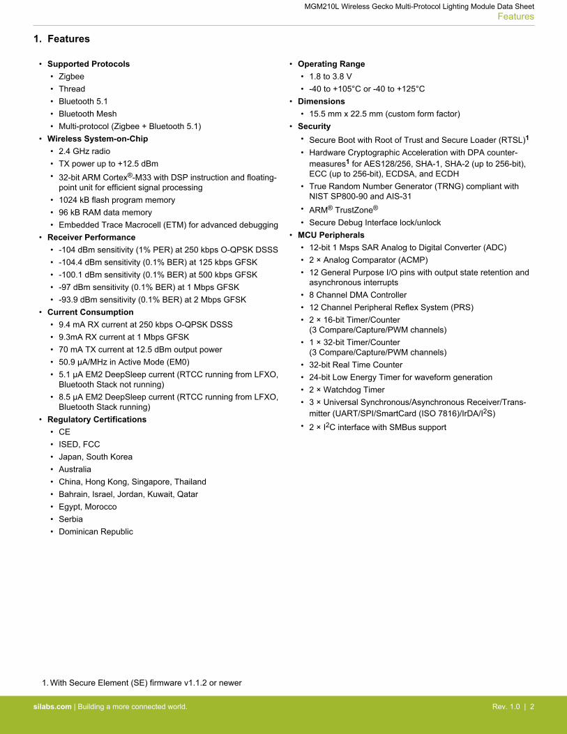
1. Features
• Supported Protocols• Zigbee• Thread• Bluetooth 5.1• Bluetooth Mesh• Multi-protocol (Zigbee + Bluetooth 5.1)
• Wireless System-on-Chip• 2.4 GHz radio• TX power up to +12.5 dBm• 32-bit ARM Cortex®-M33 with DSP instruction and floating-
point unit for efficient signal processing• 1024 kB flash program memory• 96 kB RAM data memory• Embedded Trace Macrocell (ETM) for advanced debugging
• Receiver Performance• -104 dBm sensitivity (1% PER) at 250 kbps O-QPSK DSSS• -104.4 dBm sensitivity (0.1% BER) at 125 kbps GFSK• -100.1 dBm sensitivity (0.1% BER) at 500 kbps GFSK• -97 dBm sensitivity (0.1% BER) at 1 Mbps GFSK• -93.9 dBm sensitivity (0.1% BER) at 2 Mbps GFSK
• Current Consumption• 9.4 mA RX current at 250 kbps O-QPSK DSSS• 9.3mA RX current at 1 Mbps GFSK• 70 mA TX current at 12.5 dBm output power• 50.9 µA/MHz in Active Mode (EM0)• 5.1 μA EM2 DeepSleep current (RTCC running from LFXO,
Bluetooth Stack not running)• 8.5 μA EM2 DeepSleep current (RTCC running from LFXO,
Bluetooth Stack running)• Regulatory Certifications
• CE• ISED, FCC• Japan, South Korea• Australia• China, Hong Kong, Singapore, Thailand• Bahrain, Israel, Jordan, Kuwait, Qatar• Egypt, Morocco• Serbia• Dominican Republic
• Operating Range• 1.8 to 3.8 V• -40 to +105°C or -40 to +125°C
• Dimensions• 15.5 mm x 22.5 mm (custom form factor)
• Security• Secure Boot with Root of Trust and Secure Loader (RTSL)1
• Hardware Cryptographic Acceleration with DPA counter-measures1 for AES128/256, SHA-1, SHA-2 (up to 256-bit),ECC (up to 256-bit), ECDSA, and ECDH
• True Random Number Generator (TRNG) compliant withNIST SP800-90 and AIS-31
• ARM® TrustZone®
• Secure Debug Interface lock/unlock• MCU Peripherals
• 12-bit 1 Msps SAR Analog to Digital Converter (ADC)• 2 × Analog Comparator (ACMP)• 12 General Purpose I/O pins with output state retention and
asynchronous interrupts• 8 Channel DMA Controller• 12 Channel Peripheral Reflex System (PRS)• 2 × 16-bit Timer/Counter
(3 Compare/Capture/PWM channels)• 1 × 32-bit Timer/Counter
(3 Compare/Capture/PWM channels)• 32-bit Real Time Counter• 24-bit Low Energy Timer for waveform generation• 2 × Watchdog Timer• 3 × Universal Synchronous/Asynchronous Receiver/Trans-
mitter (UART/SPI/SmartCard (ISO 7816)/IrDA/I2S)• 2 × I2C interface with SMBus support
1. With Secure Element (SE) firmware v1.1.2 or newer
MGM210L Wireless Gecko Multi-Protocol Lighting Module Data SheetFeatures
silabs.com | Building a more connected world. Rev. 1.0 | 2

2. Ordering Information
Table 2.1. Ordering Information
Ordering Code Protocol StackMax TXPower
FreqBand Antenna
Flash(kB)
RAM(kB) GPIO Temp Range Packaging
MGM210LA22JIF2 • Zigbee• Thread• Bluetooth 5.1
12.5 dBm 2.4 GHz Inverted-FPCB Trace
1024 96 12 -40 to 125 °C Cut Tape
MGM210LA22JIF2R • Zigbee• Thread• Bluetooth 5.1
12.5 dBm 2.4 GHz Inverted-FPCB Trace
1024 96 12 -40 to 125 °C Reel
MGM210LA22JNF2 • Zigbee• Thread• Bluetooth 5.1
12.5 dBm 2.4 GHz Inverted-FPCB Trace
1024 96 12 -40 to 105 °C Cut Tape
MGM210LA22JNF2R • Zigbee• Thread• Bluetooth 5.1
12.5 dBm 2.4 GHz Inverted-FPCB Trace
1024 96 12 -40 to 105 °C Reel
End-product manufacturers must verify that the module is configured to meet regulatory limits for each region in accordance with theformal certification test reports.
MGM210L modules are pre-programmed with UART XMODEM bootloader.
SLWRB4309B radio board is available for MGM210L evaluation and development.
The modules may be referred to by their product family name (MGM210L), model name (MGM210L22F) or full ordering code through-out this document.
MGM210L Wireless Gecko Multi-Protocol Lighting Module Data SheetOrdering Information
silabs.com | Building a more connected world. Rev. 1.0 | 3

Table of Contents1. Features . . . . . . . . . . . . . . . . . . . . . . . . . . . . . . . . . 2
2. Ordering Information . . . . . . . . . . . . . . . . . . . . . . . . . . . . 3
3. System Overview . . . . . . . . . . . . . . . . . . . . . . . . . . . . . . 63.1 Block Diagram . . . . . . . . . . . . . . . . . . . . . . . . . . . . . . 6
3.2 EFR32MG21 SoC . . . . . . . . . . . . . . . . . . . . . . . . . . . . . 6
3.3 Antenna . . . . . . . . . . . . . . . . . . . . . . . . . . . . . . . . 6
3.4 Power Supply . . . . . . . . . . . . . . . . . . . . . . . . . . . . . . 6
4. Electrical Specifications . . . . . . . . . . . . . . . . . . . . . . . . . . . 74.1 Electrical Characteristics . . . . . . . . . . . . . . . . . . . . . . . . . . 7
4.1.1 Absolute Maximum Ratings . . . . . . . . . . . . . . . . . . . . . . . . 74.1.2 General Operating Conditions . . . . . . . . . . . . . . . . . . . . . . . 84.1.3 MCU Current Consumption at 3.0V. . . . . . . . . . . . . . . . . . . . . . 94.1.4 Radio Current Consumption at 3.0V . . . . . . . . . . . . . . . . . . . . .104.1.5 RF Transmitter General Characteristics for the 2.4 GHz Band. . . . . . . . . . . . .114.1.6 RF Transmitter Characteristics for 802.15.4 DSSS-OQPSK in the 2.4 GHz Band . . . . . .114.1.7 RF Receiver General Characteristics for the 2.4 GHz Band . . . . . . . . . . . . .114.1.8 RF Receiver Characteristics for 802.15.4 DSSS-OQPSK in the 2.4 GHz Band . . . . . . .124.1.9 RF Receiver Characteristics for Bluetooth Low Energy at 1 Mbps . . . . . . . . . . .134.1.10 RF Receiver Characteristics for Bluetooth Low Energy at 2 Mbps . . . . . . . . . . .144.1.11 RF Receiver Characteristics for Bluetooth Low Energy at 500 kbps . . . . . . . . . .154.1.12 RF Receiver Characteristics for Bluetooth Low Energy at 125 kbps . . . . . . . . . .164.1.13 High-Frequency Crystal . . . . . . . . . . . . . . . . . . . . . . . . .174.1.14 GPIO Pins . . . . . . . . . . . . . . . . . . . . . . . . . . . . .174.1.15 Microcontroller Peripherals . . . . . . . . . . . . . . . . . . . . . . . .18
4.2 Typical Performance Curves . . . . . . . . . . . . . . . . . . . . . . . . .184.2.1 Antenna Radiation and Efficiency . . . . . . . . . . . . . . . . . . . . . .19
5. Reference Diagrams. . . . . . . . . . . . . . . . . . . . . . . . . . . . 20
6. Pin Definitions . . . . . . . . . . . . . . . . . . . . . . . . . . . . . . 216.1 Module Pinout . . . . . . . . . . . . . . . . . . . . . . . . . . . . . .21
6.2 Alternate Pin Functions . . . . . . . . . . . . . . . . . . . . . . . . . . .22
6.3 Analog Peripheral Connectivity . . . . . . . . . . . . . . . . . . . . . . . .22
6.4 Digital Peripheral Connectivity . . . . . . . . . . . . . . . . . . . . . . . . .23
7. Design Guidelines . . . . . . . . . . . . . . . . . . . . . . . . . . . . 267.1 Module Placement. . . . . . . . . . . . . . . . . . . . . . . . . . . . .26
7.2 Antenna Optimization. . . . . . . . . . . . . . . . . . . . . . . . . . . .27
7.3 Reset . . . . . . . . . . . . . . . . . . . . . . . . . . . . . . . . .27
7.4 Debug . . . . . . . . . . . . . . . . . . . . . . . . . . . . . . . . .27
7.5 Packet Trace Interface (PTI) . . . . . . . . . . . . . . . . . . . . . . . . .28
silabs.com | Building a more connected world. Rev. 1.0 | 4

8. Package Specifications . . . . . . . . . . . . . . . . . . . . . . . . . . 298.1 Package Outline . . . . . . . . . . . . . . . . . . . . . . . . . . . . .29
8.2 PCB Land Pattern . . . . . . . . . . . . . . . . . . . . . . . . . . . . .30
8.3 Package Marking . . . . . . . . . . . . . . . . . . . . . . . . . . . . .31
9. Soldering Recommendations . . . . . . . . . . . . . . . . . . . . . . . . 32
10. Tape and Reel . . . . . . . . . . . . . . . . . . . . . . . . . . . . .33
11. Certifications . . . . . . . . . . . . . . . . . . . . . . . . . . . . . . 3411.1 CE . . . . . . . . . . . . . . . . . . . . . . . . . . . . . . . . .34
11.2 FCC . . . . . . . . . . . . . . . . . . . . . . . . . . . . . . . . .35
11.3 ISED Canada . . . . . . . . . . . . . . . . . . . . . . . . . . . . . .36
11.4 Australia & New Zealand . . . . . . . . . . . . . . . . . . . . . . . . . .37
11.5 Dominican Republic . . . . . . . . . . . . . . . . . . . . . . . . . . . .37
11.6 Hong Kong . . . . . . . . . . . . . . . . . . . . . . . . . . . . . . .38
11.7 Israel . . . . . . . . . . . . . . . . . . . . . . . . . . . . . . . . .38
11.8 Jordan . . . . . . . . . . . . . . . . . . . . . . . . . . . . . . . .38
11.9 Kuwait . . . . . . . . . . . . . . . . . . . . . . . . . . . . . . . .38
11.10 Serbia . . . . . . . . . . . . . . . . . . . . . . . . . . . . . . . .38
11.11 Singapore. . . . . . . . . . . . . . . . . . . . . . . . . . . . . . .38
11.12 Kingdom of Bahrain . . . . . . . . . . . . . . . . . . . . . . . . . . .38
11.13 China . . . . . . . . . . . . . . . . . . . . . . . . . . . . . . . .38
11.14 Egypt . . . . . . . . . . . . . . . . . . . . . . . . . . . . . . . .38
11.15 Japan . . . . . . . . . . . . . . . . . . . . . . . . . . . . . . . .39
11.16 KC South Korea . . . . . . . . . . . . . . . . . . . . . . . . . . . .39
11.17 Morocco . . . . . . . . . . . . . . . . . . . . . . . . . . . . . . .39
11.18 Qatar . . . . . . . . . . . . . . . . . . . . . . . . . . . . . . . .39
11.19 Thailand . . . . . . . . . . . . . . . . . . . . . . . . . . . . . . .40
12. Revision History. . . . . . . . . . . . . . . . . . . . . . . . . . . . . 41
silabs.com | Building a more connected world. Rev. 1.0 | 5

3. System Overview
3.1 Block Diagram
The MGM210L module is a highly-integrated, high-performance system with all the hardware components needed to enable 2.4 GHzwireless connectivity and support robust networking capabilities via multiple protocols.
Built around the EFR32MG21 Wireless Gecko SoC, the MGM210L includes a built-in PCB trace antenna, an RF matching network (op-timized for transmit power efficiency), supply decoupling and filtering components, a 38.4 MHz reference crystal, and an RF shield. Ageneral block diagram of the module is shown below.
DEC
Silicon LabsEFR32MG21
HF XTAL
Supply Decoupling
RF SHIELD
VDD
GPIO
GND
(up to 12)RF Match
Antenna
LPF
Figure 3.1. MGM210L Block Diagram
3.2 EFR32MG21 SoC
The EFR32MG21 SoC features a 32-bit ARM Cortex M33 core, a 2.4 GHz high-performance radio, 1 MB of Flash memory, a dedicatedcore for security, a rich set of MCU peripherals, and various clock management and serial interfacing options. Consult the EFR32xG21Wireless Gecko Reference Manual and the EFR32MG21 Data Sheet for details.
3.3 Antenna
MGM210L modules include a meandered inverted-F antenna (MIFA) with the characteristics seen below.
Table 3.1. Antenna Efficiency and Peak Gain
Parameter With optimal layout Note
Efficiency -2 to -2.5 dB Antenna efficiency, gain and radiation pattern are highly depend-ent on the application PCB layout and mechanical design. Referto Section 7. Design Guidelines for PCB layout and antenna inte-gration guidelines to achieve optimal performance.
Peak gain 0.5 dBi
3.4 Power Supply
The MGM210L requires a single nominal supply level of 3.0 V. All the necessary decoupling and filtering components are included inthe module. The module can tolerate supply voltage noise of up to 700 mVpp.
The supply voltage is filtered internally in the module with a 100 kHz low-pass filter to guarantee operation across the full supply rangeof 1.8 to 3.8 V. Additional external filtering is neither required nor recommended as it may cause voltage drops below the minimum leveltolerable by the SoC (1.71 V) during transmit bursts.
For typical use cases, the decouple pin (DEC) should be left disconnected.
MGM210L Wireless Gecko Multi-Protocol Lighting Module Data SheetSystem Overview
silabs.com | Building a more connected world. Rev. 1.0 | 6

4. Electrical Specifications
4.1 Electrical Characteristics
All electrical parameters in all tables are specified under the following conditions, unless stated otherwise:• Typical values are based on TA=25 °C and VDD = 3.0 V, by production test and/or technology characterization.• Radio performance numbers are measured in conducted mode, based on Silicon Laboratories reference designs using output pow-
er-specific external RF impedance-matching networks for interfacing to a 50 Ω antenna.• Minimum and maximum values represent the worst conditions across supply voltage, process variation, and operating temperature,
unless stated otherwise.
4.1.1 Absolute Maximum Ratings
Stresses above those listed below may cause permanent damage to the device. This is a stress rating only and functional operation ofthe devices at those or any other conditions above those indicated in the operation listings of this specification is not implied. Exposureto maximum rating conditions for extended periods may affect device reliability. For more information on the available quality and relia-bility data, see the Quality and Reliability Monitor Report at http://www.silabs.com/support/quality/pages/default.aspx.
Table 4.1. Absolute Maximum Ratings
Parameter Symbol Test Condition Min Typ Max Unit
Storage temperature range TSTG -50 — +150 °C
Voltage on VDD supply pin VDDMAX -0.3 — 3.8 V
Voltage ramp rate on VDDsupply pin
VDDRAMPMAX — — 1.0 V / µs
DC voltage on any GPIO pin VDIGPIN -0.3 — VDD + 0.3 V
Total current into VDD pin IVDDMAX Source — — 200 mA
Total current into GND pin IGNDMAX Sink — — 200 mA
Current per I/O pin IIOMAX Sink — — 50 mA
Source — — 50 mA
Current for all I/O pins IIOALLMAX Sink — — 200 mA
Source — — 200 mA
Junction temperature TJMAX — — +125 °C
MGM210L Wireless Gecko Multi-Protocol Lighting Module Data SheetElectrical Specifications
silabs.com | Building a more connected world. Rev. 1.0 | 7

4.1.2 General Operating Conditions
This table specifies the general operating temperature range and supply voltage range for all supplies. The minimum and maximumvalues of all other tables are specifed over this operating range, unless otherwise noted.
Table 4.2. General Operating Conditions
Parameter Symbol Test Condition Min Typ Max Unit
Operating ambient tempera-ture range
TA -N temperature grade -40 — +105 °C
-I temperature grade -40 — +125 ° C
VDD Supply Voltage VDD 1.8 3.0 3.8 V
HCLK and Core frequency fHCLK MODE = WS1, RAMWSEN = 11 — — 80 MHz
MODE = WS1, RAMWSEN = 01 — — 50 MHz
MODE = WS0, RAMWSEN = 01 — — 39 MHz
PCLK frequency fPCLK — — 50 MHz
EM01 Group A clock fre-quency
fEM01GRPACLK — — 80 MHz
HCLK Radio frequency fHCLKRADIO — 38.4 — MHz
Note:1. Flash wait states are set by the MODE field in the MSC_READCTRL register. RAM wait states are enabled by setting the RAMW-
SEN bit in the SYSYCFG_DMEM0RAMCTRL register.
MGM210L Wireless Gecko Multi-Protocol Lighting Module Data SheetElectrical Specifications
silabs.com | Building a more connected world. Rev. 1.0 | 8
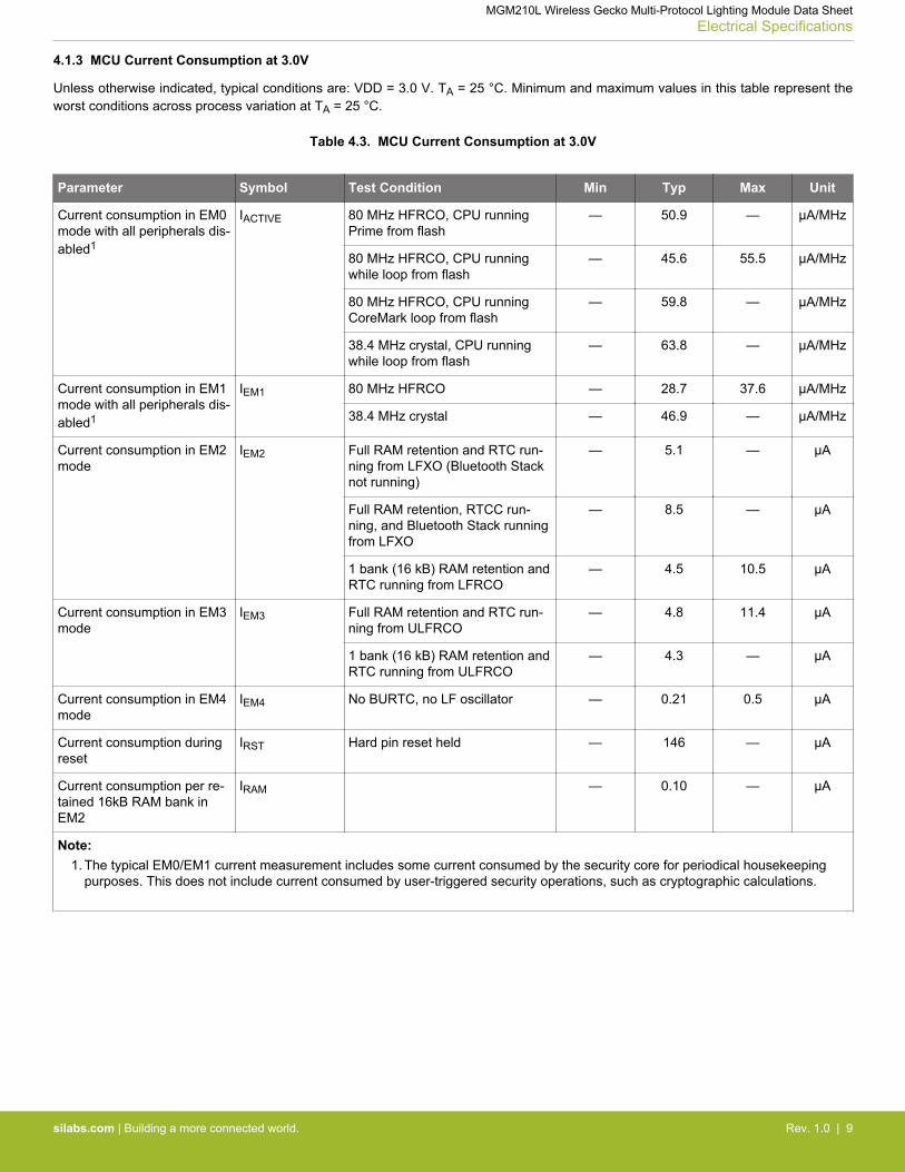
4.1.3 MCU Current Consumption at 3.0V
Unless otherwise indicated, typical conditions are: VDD = 3.0 V. TA = 25 °C. Minimum and maximum values in this table represent theworst conditions across process variation at TA = 25 °C.
Table 4.3. MCU Current Consumption at 3.0V
Parameter Symbol Test Condition Min Typ Max Unit
Current consumption in EM0mode with all peripherals dis-abled1
IACTIVE 80 MHz HFRCO, CPU runningPrime from flash
— 50.9 — µA/MHz
80 MHz HFRCO, CPU runningwhile loop from flash
— 45.6 55.5 µA/MHz
80 MHz HFRCO, CPU runningCoreMark loop from flash
— 59.8 — µA/MHz
38.4 MHz crystal, CPU runningwhile loop from flash
— 63.8 — µA/MHz
Current consumption in EM1mode with all peripherals dis-abled1
IEM1 80 MHz HFRCO — 28.7 37.6 µA/MHz
38.4 MHz crystal — 46.9 — µA/MHz
Current consumption in EM2mode
IEM2 Full RAM retention and RTC run-ning from LFXO (Bluetooth Stacknot running)
— 5.1 — µA
Full RAM retention, RTCC run-ning, and Bluetooth Stack runningfrom LFXO
— 8.5 — µA
1 bank (16 kB) RAM retention andRTC running from LFRCO
— 4.5 10.5 µA
Current consumption in EM3mode
IEM3 Full RAM retention and RTC run-ning from ULFRCO
— 4.8 11.4 µA
1 bank (16 kB) RAM retention andRTC running from ULFRCO
— 4.3 — µA
Current consumption in EM4mode
IEM4 No BURTC, no LF oscillator — 0.21 0.5 µA
Current consumption duringreset
IRST Hard pin reset held — 146 — µA
Current consumption per re-tained 16kB RAM bank inEM2
IRAM — 0.10 — µA
Note:1. The typical EM0/EM1 current measurement includes some current consumed by the security core for periodical housekeeping
purposes. This does not include current consumed by user-triggered security operations, such as cryptographic calculations.
MGM210L Wireless Gecko Multi-Protocol Lighting Module Data SheetElectrical Specifications
silabs.com | Building a more connected world. Rev. 1.0 | 9

4.1.4 Radio Current Consumption at 3.0V
RF current consumption measured with MCU in EM1, HCLK = 38.4 MHz, and all MCU peripherals disabled. Unless otherwise indica-ted, typical conditions are: VDD = 3.0V. TA = 25 °C. Minimum and maximum values in this table represent the worst conditions acrossprocess variation at TA = 25 °C.
Table 4.4. Radio Current Consumption at 3.0V
Parameter Symbol Test Condition Min Typ Max Unit
Current consumption in re-ceive mode, active packetreception
IRX_ACTIVE 125 kbit/s, 2GFSK, f = 2.4 GHz,Bluetooth stack running
— 9.3 — mA
500 kbit/s, 2GFSK, f = 2.4 GHz,Bluetooth stack running
— 9.3 — mA
1 Mbit/s, 2GFSK, f = 2.4 GHz,Bluetooth stack running
— 9.3 — mA
2 Mbit/s, 2GFSK, f = 2.4 GHz,Bluetooth stack running
— 9.9 — mA
802.15.4 receiving frame, f = 2.4GHz, ZigBee stack running
— 9.4 — mA
Current consumption in re-ceive mode, Stack running
IRX_LISTEN 125 kbit/s, 2GFSK, f = 2.4 GHz,Bluetooth stack running
— 9.1 — mA
500 kbit/s, 2GFSK, f = 2.4 GHz,Bluetooth stack running
— 9.1 — mA
1 Mbit/s, 2GFSK, f = 2.4 GHz,Bluetooth stack running
— 9.1 — mA
2 Mbit/s, 2GFSK, f = 2.4 GHz,Bluetooh stack running
— 9.8 — mA
802.15.4, f = 2.4 GHz, ZigBeestack running
— 9.2 — mA
Current consumption intransmit mode
ITX f = 2.4 GHz, CW, 12.5 dBm outputpower, VDD = 3.3 V
— 70 — mA
MGM210L Wireless Gecko Multi-Protocol Lighting Module Data SheetElectrical Specifications
silabs.com | Building a more connected world. Rev. 1.0 | 10

4.1.5 RF Transmitter General Characteristics for the 2.4 GHz Band
Unless otherwise indicated, typical conditions are: TA = 25 °C, VDD = 3.0V. RF center frequency 2.45 GHz. 1
Table 4.5. RF Transmitter General Characteristics for the 2.4 GHz Band
Parameter Symbol Test Condition Min Typ Max Unit
RF tuning frequency range FRANGE 2400 — 2483.5 MHz
Maximum TX power 23 POUTMAX 12 dBm PA, VDD = 3.3 V — 12.5 — dBm
Minimum active TX Power POUTMIN 12 dBm PA, VDD = 3.3 V — -20.5 — dBm
Output power variation vsVDD supply voltage varia-tion, frequency = 2450MHz
POUTVAR_V 12 dBm PA Pout = POUTMAX out-put power with VDD voltage sweptfrom 3.8V to 3.0V.
— +/- 0.5 — dB
12 dBm PA Pout = POUTMAX out-put power with VDD voltage sweptfrom 3.8V to 1.8V
— +0.5/-4.5 — dB
Output power variation vs RFfrequency
POUTVAR_F 12 dBm PA, POUTMAX, VDD =3.3 V.
— +/- 0.1 — dB
Note:1. For regulatory compliance please refer to the official certification test reports2. Supported transmit power levels are determined by the ordering part number (OPN). Transmit power ratings for all devices cov-
ered in this data sheet can be found in the TX Power column of the Ordering Information Table.3. The maximum TXP to comply with ETSI PSD and EIRP limits depend on antenna gain which in turn depend on the end product
mechanical design. In optimal conditions the module is compliant to the ETSI PSD and EIRP limits at maximum TXP of 8.2 dBm.End product manufacturer must ensure compliance to the limits for CE marking of the end product.
4.1.6 RF Transmitter Characteristics for 802.15.4 DSSS-OQPSK in the 2.4 GHz Band
Unless otherwise indicated, typical conditions are: TA = 25 °C, VDD = 3.0V. RF center frequency 2.45 GHz.
Table 4.6. RF Transmitter Characteristics for 802.15.4 DSSS-OQPSK in the 2.4 GHz Band
Parameter Symbol Test Condition Min Typ Max Unit
Error vector magnitude per802.15.4-2011
EVM Average across frequency, signalis DSSS-OQPSK reference pack-et, VDD = 3.3 V, Pout = POUTMAX
— 2.7 — % rms
4.1.7 RF Receiver General Characteristics for the 2.4 GHz Band
Unless otherwise indicated, typical conditions are: TA = 25 °C, VDD = 3.0V. RF center frequency 2.45 GHz.
Table 4.7. RF Receiver General Characteristics for the 2.4 GHz Band
Parameter Symbol Test Condition Min Typ Max Unit
RF tuning frequency range FRANGE 2400 — 2483.5 MHz
MGM210L Wireless Gecko Multi-Protocol Lighting Module Data SheetElectrical Specifications
silabs.com | Building a more connected world. Rev. 1.0 | 11

4.1.8 RF Receiver Characteristics for 802.15.4 DSSS-OQPSK in the 2.4 GHz Band
Unless otherwise indicated, typical conditions are: TA = 25 °C, VDD = 3.0V. RF center frequency 2.45 GHz.
Table 4.8. RF Receiver Characteristics for 802.15.4 DSSS-OQPSK in the 2.4 GHz Band
Parameter Symbol Test Condition Min Typ Max Unit
Max usable receiver inputlevel, 1% PER
SAT Signal is reference signal1, packetlength is 20 octets
— 10 — dBm
Sensitivity, 1% PER SENS Signal is reference signal, packetlength is 20 octets
— -104 — dBm
Co-channel interferer rejec-tion, 1% PER
CCR Desired signal 3 dB above sensi-tivity limit
— -0.2 — dB
Adjacent channel rejection,Interferer is reference signal,1% PER, desired is refer-ence signal at 3 dB abovereference sensitivity level2
ACRREF1 Interferer is reference signal at +1channel spacing
— 39.9 — dB
Interferer is reference signal at -1channel spacing
— 39.2 — dB
Alternate channel rejection,interferer is reference signal,1% PER, desired is refer-ence signal at 3 dB abovereference sensitivity level2
ACRREF2 Interferer is reference signal at +2channel spacing
— 51.1 — dB
Interferer is reference signal at -2channel spacing
— 51.6 — dB
Image rejection, 1% PER,desired is reference signal at3 dB above reference sensi-tivity level2
IR Interferer is CW in image band3 — 43.5 — dB
Blocking rejection of all otherchannels, 1% PER, desiredis reference signal at 3 dBabove reference sensitivitylevel2, interferer is referencesignal
BLOCK Interferer frequency < desired fre-quency -3 channel spacing
— 57.6 — dB
Interferer frequency > desired fre-quency +3 channel spacing
— 57.5 — dB
RSSI resolution RSSIRES -100 dBm to +5 dBm — 0.25 — dB
RSSI accuracy in the linearregion as defined by802.15.4-2003
RSSILIN — +/-6 — dB
Note:1. Reference signal is defined as O-QPSK DSSS per 802.15.4, Frequency range = 2400-2483.5 MHz, Symbol rate = 62.5 ksym-
bols/s.2. Reference sensitivity level is -85 dBm.3. Due to low-IF frequency, there is some overlap of adjacent channel and image channel bands. Adjacent channel CW blocker
tests place the Interferer center frequency at the Desired frequency ± 5 MHz on the channel raster, whereas the image rejectiontest places the CW interferer near the image frequency of the Desired signal carrier, regardless of the channel raster.
MGM210L Wireless Gecko Multi-Protocol Lighting Module Data SheetElectrical Specifications
silabs.com | Building a more connected world. Rev. 1.0 | 12

4.1.9 RF Receiver Characteristics for Bluetooth Low Energy at 1 Mbps
Unless otherwise indicated, typical conditions are: TA = 25 °C, VDD = 3.0V. RF center frequency 2.45 GHz.
Table 4.9. RF Receiver Characteristics for Bluetooth Low Energy at 1 Mbps
Parameter Symbol Test Condition Min Typ Max Unit
Max usable receiver inputlevel
SAT Signal is reference signal, packetlength is 37 bytes1
— 10 — dBm
Sensitivity SENS Signal is reference signal, 37 bytepayload1
— -97 — dBm
With non-ideal signals2 1 — -96.5 — dBm
Signal to co-channel interfer-er
C/ICC (see notes)1 3 — +6.6 — dB
N ± 1 Adjacent channel se-lectivity
C/I1 Interferer is reference signal at +1MHz offset1 4 3 5
— -8.3 — dB
Interferer is reference signal at -1MHz offset1 4 3 5
— -8.7 — dB
N ± 2 Alternate channel se-lectivity
C/I2 Interferer is reference signal at +2MHz offset1 4 3 5
— -42.1 — dB
Interferer is reference signal at -2MHz offset1 4 3 5
— -48.9 — dB
N ± 3 Alternate channel se-lectivity
C/I3 Interferer is reference signal at +3MHz offset1 4 3 5
— -42.4 — dB
Interferer is reference signal at -3MHz offset1 4 3 5
— -54.8 — dB
Selectivity to image frequen-cy
C/IIM Interferer is reference signal at im-age frequency with 1 MHz preci-sion1 5
— -42.1 — dB
Selectivity to image frequen-cy ± 1 MHz
C/IIM_1 Interferer is reference signal at im-age frequency +1 MHz with 1MHz precision1 5
— -42.4 — dB
Interferer is reference signal at im-age frequency -1 MHz with 1 MHzprecision1 5
— -8.3 — dB
Intermodulation performance IM n = 3 6 — -23 — dBm
Note:1. 0.1% Bit Error Rate.2. With non-ideal signals as specified in Bluetooth Test Specification RF-PHY.TS.5.0.1 section 4.7.13. Desired signal -67 dBm.4. Desired frequency 2402 MHz ≤ Fc ≤ 2480 MHz.5. With allowed exceptions.6. As specified in Bluetooth Core specification version 5.1, Vol 6, Part A, Section 4.4
MGM210L Wireless Gecko Multi-Protocol Lighting Module Data SheetElectrical Specifications
silabs.com | Building a more connected world. Rev. 1.0 | 13
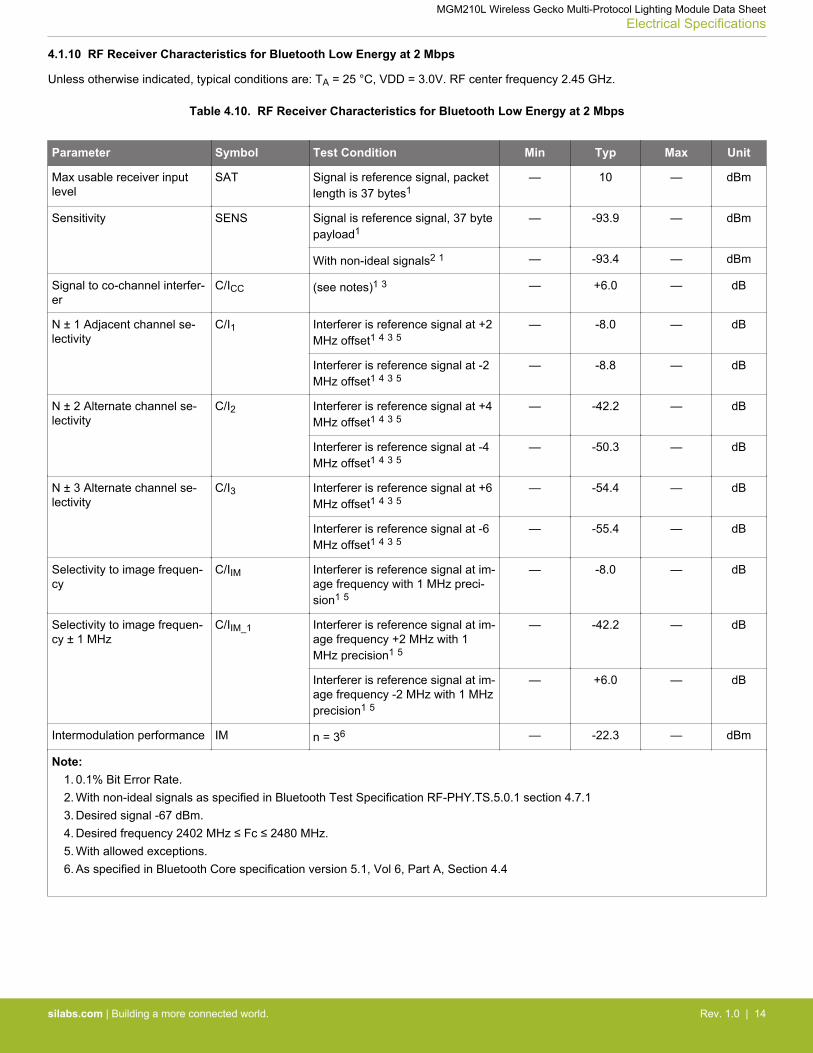
4.1.10 RF Receiver Characteristics for Bluetooth Low Energy at 2 Mbps
Unless otherwise indicated, typical conditions are: TA = 25 °C, VDD = 3.0V. RF center frequency 2.45 GHz.
Table 4.10. RF Receiver Characteristics for Bluetooth Low Energy at 2 Mbps
Parameter Symbol Test Condition Min Typ Max Unit
Max usable receiver inputlevel
SAT Signal is reference signal, packetlength is 37 bytes1
— 10 — dBm
Sensitivity SENS Signal is reference signal, 37 bytepayload1
— -93.9 — dBm
With non-ideal signals2 1 — -93.4 — dBm
Signal to co-channel interfer-er
C/ICC (see notes)1 3 — +6.0 — dB
N ± 1 Adjacent channel se-lectivity
C/I1 Interferer is reference signal at +2MHz offset1 4 3 5
— -8.0 — dB
Interferer is reference signal at -2MHz offset1 4 3 5
— -8.8 — dB
N ± 2 Alternate channel se-lectivity
C/I2 Interferer is reference signal at +4MHz offset1 4 3 5
— -42.2 — dB
Interferer is reference signal at -4MHz offset1 4 3 5
— -50.3 — dB
N ± 3 Alternate channel se-lectivity
C/I3 Interferer is reference signal at +6MHz offset1 4 3 5
— -54.4 — dB
Interferer is reference signal at -6MHz offset1 4 3 5
— -55.4 — dB
Selectivity to image frequen-cy
C/IIM Interferer is reference signal at im-age frequency with 1 MHz preci-sion1 5
— -8.0 — dB
Selectivity to image frequen-cy ± 1 MHz
C/IIM_1 Interferer is reference signal at im-age frequency +2 MHz with 1MHz precision1 5
— -42.2 — dB
Interferer is reference signal at im-age frequency -2 MHz with 1 MHzprecision1 5
— +6.0 — dB
Intermodulation performance IM n = 36 — -22.3 — dBm
Note:1. 0.1% Bit Error Rate.2. With non-ideal signals as specified in Bluetooth Test Specification RF-PHY.TS.5.0.1 section 4.7.13. Desired signal -67 dBm.4. Desired frequency 2402 MHz ≤ Fc ≤ 2480 MHz.5. With allowed exceptions.6. As specified in Bluetooth Core specification version 5.1, Vol 6, Part A, Section 4.4
MGM210L Wireless Gecko Multi-Protocol Lighting Module Data SheetElectrical Specifications
silabs.com | Building a more connected world. Rev. 1.0 | 14

4.1.11 RF Receiver Characteristics for Bluetooth Low Energy at 500 kbps
Unless otherwise indicated, typical conditions are: TA = 25 °C, VDD = 3.0V. RF center frequency 2.45 GHz.
Table 4.11. RF Receiver Characteristics for Bluetooth Low Energy at 500 kbps
Parameter Symbol Test Condition Min Typ Max Unit
Max usable receiver inputlevel
SAT Signal is reference signal, packetlength is 37 bytes1
— 10 — dBm
Sensitivity SENS Signal is reference signal1 — -100.1 — dBm
With non-ideal signals2 1 — -99.5 — dBm
Signal to co-channel interfer-er
C/ICC (see notes)1 3 — +2.1 — dB
N ± 1 Adjacent channel se-lectivity
C/I1 Interferer is reference signal at +1MHz offset1 4 3 5
— -9.0 — dB
Interferer is reference signal at -1MHz offset1 4 3 5
— -9.5 — dB
N ± 2 Alternate channel se-lectivity
C/I2 Interferer is reference signal at +2MHz offset1 4 3 5
— -44.4 — dB
Interferer is reference signal at -2MHz offset1 4 3 5
— -51.9 — dB
N ± 3 Alternate channel se-lectivity
C/I3 Interferer is reference signal at +3MHz offset1 4 3 5
— -44.3 — dB
Interferer is reference signal at -3MHz offset1 4 3 5
— -58.3 — dB
Selectivity to image frequen-cy
C/IIM Interferer is reference signal at im-age frequency with 1 MHz preci-sion1 5
— -44.4 — dB
Selectivity to image frequen-cy ± 1 MHz
C/IIM_1 Interferer is reference signal at im-age frequency +1 MHz with 1MHz precision1 5
— -44.3 — dB
Interferer is reference signal at im-age frequency -1 MHz with 1 MHzprecision1 5
— -9.0 — dB
Note:1. 0.1% Bit Error Rate.2. With non-ideal signals as specified in Bluetooth Test Specification RF-PHY.TS.5.0.1 section 4.7.13. Desired signal -72 dBm.4. Desired frequency 2402 MHz ≤ Fc ≤ 2480 MHz.5. With allowed exceptions.
MGM210L Wireless Gecko Multi-Protocol Lighting Module Data SheetElectrical Specifications
silabs.com | Building a more connected world. Rev. 1.0 | 15

4.1.12 RF Receiver Characteristics for Bluetooth Low Energy at 125 kbps
Unless otherwise indicated, typical conditions are: TA = 25 °C, VDD = 3.0V. RF center frequency 2.45 GHz.
Table 4.12. RF Receiver Characteristics for Bluetooth Low Energy at 125 kbps
Parameter Symbol Test Condition Min Typ Max Unit
Max usable receiver inputlevel
SAT Signal is reference signal, packetlength is 37 bytes1
— 10 — dBm
Sensitivity SENS Signal is reference signal1 — -104.4 — dBm
With non-ideal signals2 1 — -104.1 — dBm
Signal to co-channel interfer-er
C/ICC (see notes)1 3 — +0.8 — dB
N ± 1 Adjacent channel se-lectivity
C/I1 Interferer is reference signal at +1MHz offset1 4 3 5
— -13.1 — dB
Interferer is reference signal at -1MHz offset1 4 3 5
— -13.6 — dB
N ± 2 Alternate channel se-lectivity
C/I2 Interferer is reference signal at +2MHz offset1 4 3 5
— -49.5 — dB
Interferer is reference signal at -2MHz offset1 4 3 5
— -56.9 — dB
N ± 3 Alternate channel se-lectivity
C/I3 Interferer is reference signal at +3MHz offset1 4 3 5
— -47.0 — dB
Interferer is reference signal at -3MHz offset1 4 3 5
— -63.1 — dB
Selectivity to image frequen-cy
C/IIM Interferer is reference signal at im-age frequency with 1 MHz preci-sion1 5
— -49.5 — dB
Selectivity to image frequen-cy ± 1 MHz
C/IIM_1 Interferer is reference signal at im-age frequency +1 MHz with 1MHz precision1 5
— -47.0 — dB
Interferer is reference signal at im-age frequency -1 MHz with 1 MHzprecision1 5
— -13.1 — dB
Note:1. 0.1% Bit Error Rate.2. With non-ideal signals as specified in Bluetooth Test Specification RF-PHY.TS.5.0.1 section 4.7.13. Desired signal -79 dBm.4. Desired frequency 2402 MHz ≤ Fc ≤ 2480 MHz.5. With allowed exceptions.
MGM210L Wireless Gecko Multi-Protocol Lighting Module Data SheetElectrical Specifications
silabs.com | Building a more connected world. Rev. 1.0 | 16

4.1.13 High-Frequency Crystal
Table 4.13. High-Frequency Crystal
Parameter Symbol Test Condition Min Typ Max Unit
Crystal frequency fHFXTAL — 38.4 — MHz
Initial calibrated accuracy ACCHFXTAL -10 — +10 ppm
Temperature drift DRIFTHFXTAL Across specified temperaturerange
-30 — +30 ppm
4.1.14 GPIO Pins
Unless otherwise indicated, typical conditions are: VDD = 3.0 V.
Table 4.14. GPIO Pins
Parameter Symbol Test Condition Min Typ Max Unit
Leakage current ILEAK_IO MODEx = DISABLED, VDD =1.71V
— 1.9 — nA
MODEx = DISABLED, VDD = 3.0V
— 2.5 — nA
Input low voltage1 VIL Any GPIO pin — — 0.3 * VDD V
Input high voltage1 VIH Any GPIO pin 0.7 * VDD — — V
Output low voltage VOL Sinking 20mA, VDD = 3.0 V — — 0.2 * VDD V
Sinking 8mA, VDD = 1.62 V — — 0.4 * VDD V
Output high voltage VOH Sourcing 20mA, VDD = 3.0 V 0.8 * VDD — — V
Sourcing 8mA, VDD = 1.62 V 0.6 * VDD — — V
GPIO rise time TGPIO_RISE VDD = 3.0V, Cload = 50pF, SLEW-RATE = 4, 10% to 90%
— 8.4 — ns
VDD = 1.7V, Cload = 50pF, SLEW-RATE = 4, 10% to 90%
— 13 — ns
GPIO fall time TGPIO_FALL VDD = 3.0V, Cload = 50pF, SLEW-RATE = 4, 90% to 10%
— 7.1 — ns
VDD = 1.7V, Cload = 50pF, SLEW-RATE = 4, 90% to 10%
— 11.9 — ns
Pull up/down resistance2 RPULL pull-up: MODEn = DISABLEDOUT=1, pull-down: MODEn =WIREDORPULLDOWN DOUT =0
35 44 55 kΩ
Maximum filtered glitch width TGF MODE = INPUT, DOUT = 1 — 26 — ns
Note:1. GPIO and RESETn input thresholds are proportional to the VDD supply.2. GPIO and RESETn pull-ups connect to the VDD supply. Pull-downs on GPIO connect to VSS.
MGM210L Wireless Gecko Multi-Protocol Lighting Module Data SheetElectrical Specifications
silabs.com | Building a more connected world. Rev. 1.0 | 17

4.1.15 Microcontroller Peripherals
The MCU peripherals set available in MGM210L modules includes:• 12-bit 1 Msps ADC• Analog Comparators• 16-bit and 32-bit Timers/Counters• 24-bit Low Energy Timer for waveform generation• 32-bit Real Time Counter• USART (UART/SPI/SmartCards/IrDA/I2S)• I2C peripheral interfaces• 12 Channel Peripheral Reflex System
For details on their electrical performance, consult the relevant portions of Section 4 in the SoC datasheet.
To learn which GPIO ports provide access to every peripheral, consult Section 6.3 Analog Peripheral Connectivity and Section6.4 Digital Peripheral Connectivity.
4.2 Typical Performance Curves
Typical performance curves indicate typical characterized performance under the stated conditions.
MGM210L Wireless Gecko Multi-Protocol Lighting Module Data SheetElectrical Specifications
silabs.com | Building a more connected world. Rev. 1.0 | 18

4.2.1 Antenna Radiation and Efficiency
Typical MGM210L antenna radiation patterns and efficiency under optimal operating conditions are plotted in the figure below. Antennagain and radiation patterns have a strong dependence on the size and shape of the application PCB the module is mounted on and,also, on the proximity of any mechanical design to the antenna.
Figure 4.1. Typical 2D Antenna Radiation Patterns and Efficiency
Top Left: Phi 0o, Top Right: Phi 90o, Bottom Left: Theta 90o, Bottom Right: Radiation Efficiency
MGM210L Wireless Gecko Multi-Protocol Lighting Module Data SheetElectrical Specifications
silabs.com | Building a more connected world. Rev. 1.0 | 19

5. Reference Diagrams
A typical application circuit for the MGM210L module is shown below.
xGM210L
17PC04 16PC03 15PC02 14GND 13VDD
12D
NC
11RES
ET
9PD
01
8PC
01
7PC
00
6 GND
5 DEC
3 PA03
2 PA02
1 PA01
4 PA04
18PC05
10PD
00
U1
SWCLKSWDIO
SWO/TDOTDI
UART
_TX
UART
_RX
RES
ET
GPI
OG
PIO
VDD
MINI SIMPLICITY CONNECTOR FOR DEBUGGING
135
246
7 89 10
J5
HEADER_10PIN_1.27MM_SMD_DUAL
UART_RXSWO/TDOSWCLKPTI_DATA
VDD
UART_RTSUART_CTSPTI_DATAPTI_SYNC
UART_TXRESET
SWDIOPTI_SYNC
Figure 5.1. MGM210L Application Schematic
Interconnection labels correspond to supported pin functions described in 7.4 Debug, 7.5 Packet Trace Interface (PTI) and 6.4 DigitalPeripheral Connectivity.
Placing the module horizontally on the end-application board permits access to all module pins. Placing it vertically restricts access topins 13 through 18 only. The reference schematic above is applicable for the former case only. Refer to 7. Design Guidelines for moredetails.
MGM210L Wireless Gecko Multi-Protocol Lighting Module Data SheetReference Diagrams
silabs.com | Building a more connected world. Rev. 1.0 | 20

6. Pin Definitions
6.1 Module Pinout
Figure 6.1. MGM210L Lighting Module Pinout
The next table shows the MGM210L pinout and general descriptions for each pin. Refer to 6.2 Alternate Pin Functions, 6.3 Analog Pe-ripheral Connectivity, and 6.4 Digital Peripheral Connectivity for details on functions and peripherals supported by GPIOs.
Table 6.1. MGM210L Lighting Module Pin Definitions
Pin Name Pin(s) Description Pin Name Pin(s) Description
PA01 1 GPIO/Debug PA02 2 GPIO/Debug
PA03 3 GPIO/Debug PA04 4 GPIO/Debug
DEC 5 Decouple1 GND 6 Ground
PC00 7 GPIO PC01 8 GPIO
PD01 9 GPIO PD00 10 GPIO
RESETn 11 Reset Pin3 DNC 12 Do not connect
VDD 13 VDD GND 14 Ground
PC02 15 GPIO2 PC03 16 GPIO2
PC04 17 GPIO2 PC05 18 GPIO2
Note:1. Available for powering module through external PMIC. Should be left disconnected typically. Do not use Decouple supply to pow-
er external circuitry.2. Internally terminated with series 56 ohm resistor.3. Connected to pull-up resistor to VDD internally. External pull-up is not required.
MGM210L Wireless Gecko Multi-Protocol Lighting Module Data SheetPin Definitions
silabs.com | Building a more connected world. Rev. 1.0 | 21

6.2 Alternate Pin Functions
Some GPIOs support alternate functions like debugging, wake-up from EM4, access to an external low frequency crystal, etc.. The fol-lowing table shows which module pins have alternate capabilities and the functions they support. Refer to the SoC's reference manualfor more information.
Table 6.2. GPIO Alternate Functions Table
GPIO Alternate Function
PA01 GPIO.SWCLK
PA02 GPIO.SWDIO
PA03 GPIO.SWV GPIO.TDO GPIO.TRACEDATA0
PA04 GPIO.TDI GPIO.TRACECLK
PC00 GPIO.EM4WU6
PD01 LFXO.LFXTAL_I LFXO.LF_EXTCLK
PD00 LFXO.LFXTAL_O
PC05 GPIO.EM4WU7
6.3 Analog Peripheral Connectivity
Many analog resources are routable and can be connected to numerous GPIO's. The table below indicates which peripherals are avali-able on each GPIO port. When a differential connection is being used Positive inputs are restricted to the EVEN pins and Negativeinputs are restricted to the ODD pins. When a single ended connection is being used positive input is avaliable on all pins. See thedevice Reference Manual for more details on the ABUS and analog peripherals.
Table 6.3. ABUS Routing Table
Peripheral Signal PA PC PD
EVEN ODD EVEN ODD EVEN ODD
ACMP0 ana_neg Yes Yes Yes Yes Yes Yes
ana_pos Yes Yes Yes Yes Yes Yes
ACMP1 ana_neg Yes Yes Yes Yes Yes Yes
ana_pos Yes Yes Yes Yes Yes Yes
IADC0 ana_neg Yes Yes Yes Yes Yes Yes
ana_pos Yes Yes Yes Yes Yes Yes
MGM210L Wireless Gecko Multi-Protocol Lighting Module Data SheetPin Definitions
silabs.com | Building a more connected world. Rev. 1.0 | 22

6.4 Digital Peripheral Connectivity
Many digital resources are routable and can be connected to numerous GPIO's. The table below indicates which peripherals are avalia-ble on each GPIO port.
Table 6.4. DBUS Routing
Peripheral.Resource PORT
PA PC PD
ACMP0.DIGOUT Available Available Available
ACMP1.DIGOUT Available Available Available
CMU.CLKIN0 Available Available
CMU.CLKOUT0 Available Available
CMU.CLKOUT1 Available Available
CMU.CLKOUT2 Available
FRC.DCLK Available Available
FRC.DFRAME Available Available
FRC.DOUT Available Available
I2C0.SCL Available Available Available
I2C0.SDA Available Available Available
I2C1.SCL Available Available
I2C1.SDA Available Available
LETIMER0.OUT0 Available
LETIMER0.OUT1 Available
PRS.ASYNCH0 Available
PRS.ASYNCH1 Available
PRS.ASYNCH10 Available Available
PRS.ASYNCH11 Available Available
PRS.ASYNCH2 Available
PRS.ASYNCH3 Available
PRS.ASYNCH4 Available
PRS.ASYNCH5 Available
PRS.ASYNCH6 Available Available
PRS.ASYNCH7 Available Available
PRS.ASYNCH8 Available Available
PRS.ASYNCH9 Available Available
PRS.SYNCH0 Available Available Available
PRS.SYNCH1 Available Available Available
PRS.SYNCH2 Available Available Available
PRS.SYNCH3 Available Available Available
MGM210L Wireless Gecko Multi-Protocol Lighting Module Data SheetPin Definitions
silabs.com | Building a more connected world. Rev. 1.0 | 23

Peripheral.Resource PORT
PA PC PD
TIMER0.CC0 Available Available Available
TIMER0.CC1 Available Available Available
TIMER0.CC2 Available Available Available
TIMER0.CDTI0 Available Available Available
TIMER0.CDTI1 Available Available Available
TIMER0.CDTI2 Available Available Available
TIMER1.CC0 Available Available Available
TIMER1.CC1 Available Available Available
TIMER1.CC2 Available Available Available
TIMER1.CDTI0 Available Available Available
TIMER1.CDTI1 Available Available Available
TIMER1.CDTI2 Available Available Available
TIMER2.CC0 Available
TIMER2.CC1 Available
TIMER2.CC2 Available
TIMER2.CDTI0 Available
TIMER2.CDTI1 Available
TIMER2.CDTI2 Available
TIMER3.CC0 Available Available
TIMER3.CC1 Available Available
TIMER3.CC2 Available Available
TIMER3.CDTI0 Available Available
TIMER3.CDTI1 Available Available
TIMER3.CDTI2 Available Available
USART0.CLK Available Available Available
USART0.CS Available Available Available
USART0.CTS Available Available Available
USART0.RTS Available Available Available
USART0.RX Available Available Available
USART0.TX Available Available Available
USART1.CLK Available
USART1.CS Available
USART1.CTS Available
USART1.RTS Available
USART1.RX Available
USART1.TX Available
MGM210L Wireless Gecko Multi-Protocol Lighting Module Data SheetPin Definitions
silabs.com | Building a more connected world. Rev. 1.0 | 24

Peripheral.Resource PORT
PA PC PD
USART2.CLK Available Available
USART2.CS Available Available
USART2.CTS Available Available
USART2.RTS Available Available
USART2.RX Available Available
USART2.TX Available Available
MGM210L Wireless Gecko Multi-Protocol Lighting Module Data SheetPin Definitions
silabs.com | Building a more connected world. Rev. 1.0 | 25

7. Design Guidelines
7.1 Module Placement
The MGM210L should be placed at the edge of the end-application PCB as seen below. The copper clearance area under the antennamust be void of traces or components to prevent parasitic loading or undesired coupling of signals or noise to the antenna. The width ofthe GND pour on the end-application PCB should match at least the width of the antenna (e.g. 12.5 mm or greater) to have negligibleeffect on antenna performance.
12.5 mm
5.0 mm
Figure 7.1. Inverted-F Antenna Clearance
MGM210L modules do not support the use of an external, alternative antenna. The U.FL connector land pattern on the top layer of themodule should not be used, populated or tampered with.
Figure 7.2 Horizontal Mounting on page 26 illustrates the placement recommended when mounting the module horizontally to an end-application PCB. It also shows examples of layout cases that will result in severe RF performance degradation for the module.
Figure 7.2. Horizontal Mounting
Vertical mounting provides mechanical design flexibility that could be advantageous for certain applications. Figure 7.3 Vertical Mount-ing on page 27 illustrates the placement recommended when mounting the module vertically to an end-application PCB. It also showslayout examples that will result in severe RF performance degradation for the module.
MGM210L Wireless Gecko Multi-Protocol Lighting Module Data SheetDesign Guidelines
silabs.com | Building a more connected world. Rev. 1.0 | 26

Notice that vertical mounting limits the number of pins available to interact with the module to six (VDD, GND and four GPIOs) whichmay be suitable for specific use cases only (e.g. to generate PWM outputs for LED control). The trade offs of vertical mounting shouldbe carefully considered prior to choosing such arrangement.
5.0 mm
Figure 7.3. Vertical Mounting
7.2 Antenna Optimization
Due to the nature of PCB trace antennas, the MGM210L is sensitive to the thickness of the application PCB on which it is mounted, aswell as to any plastics, metal or dielectric materials in close proximity to the antenna. The layout guide shown in Figure 7.2 HorizontalMounting on page 26 is optimal for an application board thickness of 0.8 mm.
For cases where the application board is of a thickness different than the optimal, the impedance and performance of the antenna maybe experimentally adjusted by
1. Cutting out the end-application PCB's FR4 material that is under the antenna, or by2. Adjusting the separation between the lower side of the antenna and the edge of the application board's GND plane underneath the
module
Impedance and performance optimization can be verified by measuring RSSI or radiated output power until either is maximized.
7.3 Reset
The MGM210L can be reset by pulling the RESET line low, by the internal watchdog timer, or by software command. All three methodsare applicable when the module is mounted horizontally on a given end-application board and, hence, all module pins are accessible.When mounted vertically, however, only the second and third methods apply.
The reset state does not provide power saving functionality and it is not recommended as a means to conserve power.
7.4 Debug
See AN958: Debugging and Programming Interfaces for Custom Designs.
MGM210L Wireless Gecko Multi-Protocol Lighting Module Data SheetDesign Guidelines
silabs.com | Building a more connected world. Rev. 1.0 | 27
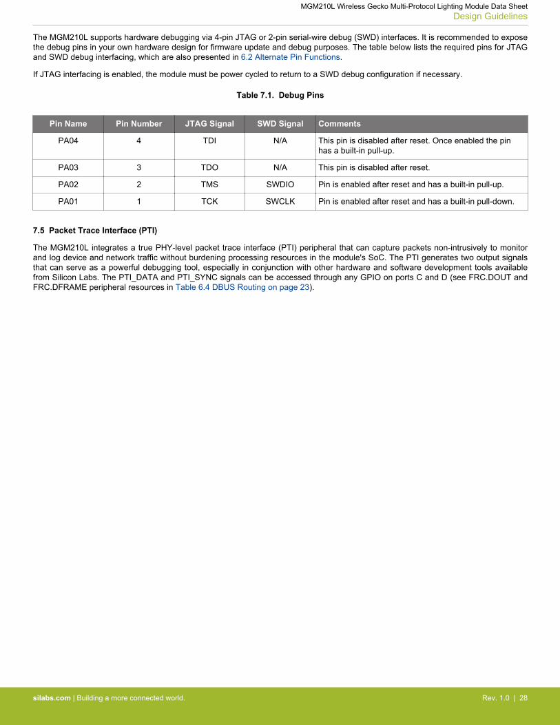
The MGM210L supports hardware debugging via 4-pin JTAG or 2-pin serial-wire debug (SWD) interfaces. It is recommended to exposethe debug pins in your own hardware design for firmware update and debug purposes. The table below lists the required pins for JTAGand SWD debug interfacing, which are also presented in 6.2 Alternate Pin Functions.
If JTAG interfacing is enabled, the module must be power cycled to return to a SWD debug configuration if necessary.
Table 7.1. Debug Pins
Pin Name Pin Number JTAG Signal SWD Signal Comments
PA04 4 TDI N/A This pin is disabled after reset. Once enabled the pinhas a built-in pull-up.
PA03 3 TDO N/A This pin is disabled after reset.
PA02 2 TMS SWDIO Pin is enabled after reset and has a built-in pull-up.
PA01 1 TCK SWCLK Pin is enabled after reset and has a built-in pull-down.
7.5 Packet Trace Interface (PTI)
The MGM210L integrates a true PHY-level packet trace interface (PTI) peripheral that can capture packets non-intrusively to monitorand log device and network traffic without burdening processing resources in the module's SoC. The PTI generates two output signalsthat can serve as a powerful debugging tool, especially in conjunction with other hardware and software development tools availablefrom Silicon Labs. The PTI_DATA and PTI_SYNC signals can be accessed through any GPIO on ports C and D (see FRC.DOUT andFRC.DFRAME peripheral resources in Table 6.4 DBUS Routing on page 23).
MGM210L Wireless Gecko Multi-Protocol Lighting Module Data SheetDesign Guidelines
silabs.com | Building a more connected world. Rev. 1.0 | 28

8. Package Specifications
8.1 Package Outline
12.5 mm
4.5 mm
5.0 mm
12.0 mm
1.0 mm
2.5 mm
13.0 mm
11.0 mm
11.5 mm
3.0 mm
2.5 mm
9.5 mm
1.35 mm
22.5 mm
0.9 mm
(±0.2)
(±0.1)(±0.1)
(±0.1)(±0.2)
(±0.1)
(±0.1)
(±0.1)
(±0.1)
(±0.1)
0.9 mm
2.25 mm(±0.2)
10.18 mm (±0.1)
15.50 mm (±0.2)
(±0.1)
Figure 8.1. Top and Side Views
Figure 8.2. Bottom View
NOTE: Solder paste thickness adds 0.1 ± 0.05 mm to overall module height
MGM210L Wireless Gecko Multi-Protocol Lighting Module Data SheetPackage Specifications
silabs.com | Building a more connected world. Rev. 1.0 | 29
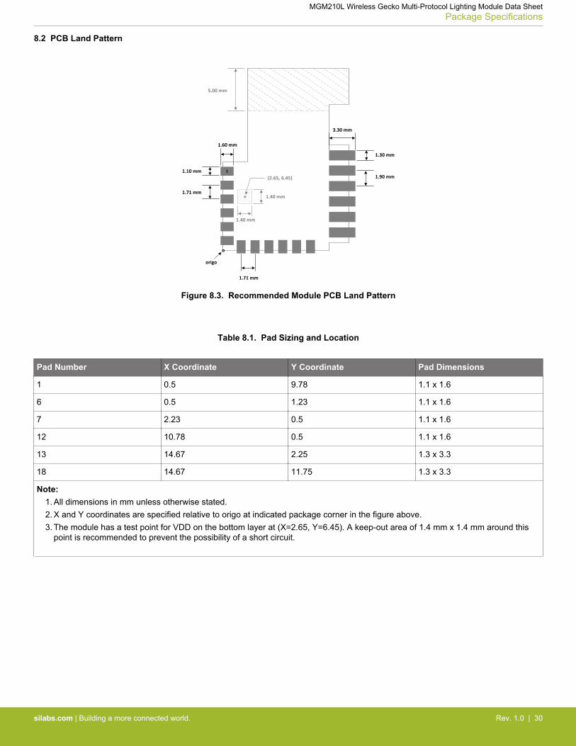
8.2 PCB Land Pattern
11.10 mm
1.71 mm
1.60 mm
3.30 mm
1.30 mm
1.90 mm
1.71 mm
origo
o
5.00 mm
1.40 mm
1.40 mm
(2.65, 6.45)
Figure 8.3. Recommended Module PCB Land Pattern
Table 8.1. Pad Sizing and Location
Pad Number X Coordinate Y Coordinate Pad Dimensions
1 0.5 9.78 1.1 x 1.6
6 0.5 1.23 1.1 x 1.6
7 2.23 0.5 1.1 x 1.6
12 10.78 0.5 1.1 x 1.6
13 14.67 2.25 1.3 x 3.3
18 14.67 11.75 1.3 x 3.3
Note:1. All dimensions in mm unless otherwise stated.2. X and Y coordinates are specified relative to origo at indicated package corner in the figure above.3. The module has a test point for VDD on the bottom layer at (X=2.65, Y=6.45). A keep-out area of 1.4 mm x 1.4 mm around this
point is recommended to prevent the possibility of a short circuit.
MGM210L Wireless Gecko Multi-Protocol Lighting Module Data SheetPackage Specifications
silabs.com | Building a more connected world. Rev. 1.0 | 30
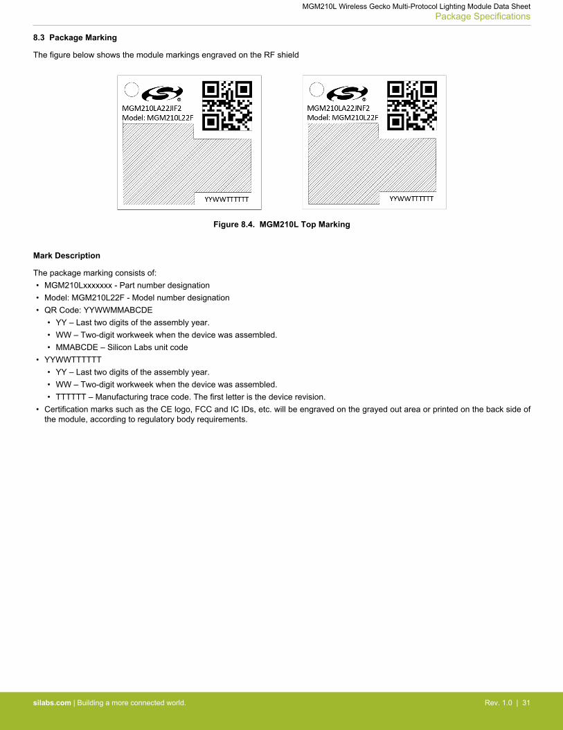
8.3 Package Marking
The figure below shows the module markings engraved on the RF shield
Figure 8.4. MGM210L Top Marking
Mark Description
The package marking consists of:• MGM210Lxxxxxxx - Part number designation• Model: MGM210L22F - Model number designation• QR Code: YYWWMMABCDE
• YY – Last two digits of the assembly year.• WW – Two-digit workweek when the device was assembled.• MMABCDE – Silicon Labs unit code
• YYWWTTTTTT• YY – Last two digits of the assembly year.• WW – Two-digit workweek when the device was assembled.• TTTTTT – Manufacturing trace code. The first letter is the device revision.
• Certification marks such as the CE logo, FCC and IC IDs, etc. will be engraved on the grayed out area or printed on the back side ofthe module, according to regulatory body requirements.
MGM210L Wireless Gecko Multi-Protocol Lighting Module Data SheetPackage Specifications
silabs.com | Building a more connected world. Rev. 1.0 | 31

9. Soldering Recommendations
It is recommended that final PCB assembly of the MGM210L follows the industry standard as identified by the Institute for Printed Cir-cuits (IPC). This product is assembled in compliance with the J-STD-001 requirements and the guidelines of IPC-AJ-820. Surfacemounting of this product by the end user is recommended to follow IPC-A-610 to meet or exceed class 2 requirements.
CLASS 1 General Electronic Products
Includes products suitable for applications where the major requirement is function of the completed assembly.
CLASS 2 Dedicated Service Electronic Products
Includes products where continued performance and extended life is required, and for which uninterrupted service is desired but notcritical. Typically the end-use environment would not cause failures.
CLASS 3 High Performance/Harsh Environment Electronic Products
Includes products where continued high performance or performance-on-demand is critical, equipment downtime cannot be tolerated,end-use environment may be uncommonly harsh, and the equipment must function when required, such as life support or other criticalsystems.
MGM210L Wireless Gecko Multi-Protocol Lighting Module Data SheetSoldering Recommendations
silabs.com | Building a more connected world. Rev. 1.0 | 32

10. Tape and Reel
All dimensions are given in mm unless otherwise indicated.
Figure 10.1. Carrier Tape Dimensions
Figure 10.2. Reel Dimensions
MGM210L Wireless Gecko Multi-Protocol Lighting Module Data SheetTape and Reel
silabs.com | Building a more connected world. Rev. 1.0 | 33
11. Certifications
This section details the regulatory certification status of the module in various regions.
The address for the module manufacturer and certification applicant is:
SILICON LABORATORIES FINLAND OYAlberga Business Park, Bertel Jungin aukio 3,02600 Espoo, Finland
11.1 CE
The MGM210L module is in conformity with the essential requirements and other relevant requirements of the Radio Equipment Direc-tive (RED) (2014/53/EU). Please note that every application using the MGM210L will need to perform the radio EMC tests on the endproduct, according to EN 301 489-17. It is ultimately the responsibility of the manufacturer to ensure the compliance of the end-product.The specific product assembly may have an impact to RF radiated characteristics, and manufacturers should carefully consider RFradiated testing with the end-product assembly. A formal Declaration of Conformity (DoC) is available via https://www.silabs.com/.
The MGM210L is compliant with EN 300 328 at nominal TX power levels of +11 dBm for Zigbee and +8 dBm for Bluetooth. The maxi-mum TX power allowed depends on the gain of the antenna which, in turn, depends on assembly characteristics of the end product.Hence, it is the end product manufacturer's responsibility to ensure compliance with the PSD and EIRP limits defined in EN 300 328.
MGM210L Wireless Gecko Multi-Protocol Lighting Module Data SheetCertifications
silabs.com | Building a more connected world. Rev. 1.0 | 34

11.2 FCC
This device complies with Part 15 of the FCC Rules. Operation is subject to the following two conditions:1. This device may not cause harmful interference, and2. This device must accept any interference received, including interference that may cause undesirable operation.
Any changes or modifications not expressly approved by Silicon Labs could void the user’s authority to operate the equipment.
FCC RF Radiation Exposure Statement:
This equipment complies with FCC radiation exposure limits set forth for an uncontrolled environment. End users must follow the specif-ic operating instructions for satisfying RF exposure compliance. This transmitter meets both portable and mobile requirements in ac-cordance to the limits exposed in the RF Exposure Analysis. This transmitter must not be co-located or operating in conjunction withany other antenna or transmitter except in accordance with FCC multi-transmitter product procedures.
OEM Responsibilities to comply with FCC Regulations:
OEM integrator is responsible for testing their end-product for any additional compliance requirements needed with this module instal-led (for example, digital device emissions, PC peripheral requirements, etc.). Additionally, investigative measurements and spot check-ing are strongly recommended to verify that the full system compliance is maintained when the module is integrated, in accordance tothe "Host Product Testing Guidance" in FCC's KDB 996369 D04 Module Integration Guide V01.• In the typical case when the integral antenna of the MGM210L is used, a minimum separation distance of 12 mm must be main-
tained at all times between the human body and the radiator (antenna) to meet the SAR exemption for portable conditions.• The transmitter module must not be co-located or operating in conjunction with any other antenna or transmitter except in accord-
ance with FCC multi-transmitter product procedures.
Important Note:
In the event that these conditions cannot be met, then for the FCC authorization to remain valid the final product will have to undergoadditional testing to evaluate the RF exposure, and a permissive change will have to be applied with the help of the customer's ownTelecommunication Certification Body.
End Product Labeling
The variants of MGM210L Modules are labeled with their own FCC ID. If the FCC ID is not visible when the module is installed insideanother device, then the outside of the device into which the module is installed must also display a label referring to the enclosedmodule. In that case, the final end product must be labeled in a visible area with the following:
"Contains Transmitter Module FCC ID: QOQMGM210L"
Or
"Contains FCC ID: QOQMGM210L"
The OEM integrator has to be aware not to provide information to the end user regarding how to install or remove this RF module orchange RF related parameters in the user manual of the end product.
Class B Device Notice
Note: This equipment has been tested and found to comply with the limits for a Class B digital device, pursuant to part 15 of the FCCRules. These limits are designed to provide reasonable protection against harmful interference in a residential installation. This equip-ment generates, uses, and can radiate radio frequency energy and, if not installed and used in accordance with the instructions, maycause harmful interference to radio communications. However, there is no guarantee that interference will not occur in a particular in-stallation. If this equipment does cause harmful interference to radio or television reception, which can be determined by turning theequipment off and on, the user is encouraged to try to correct the interference by one or more of the following measures:• Reorient or relocate the receiving antenna• Increase the separation between the equipment and receiver• Connect the equipment into an outlet on a circuit different from that to which the receiver is connected• Consult the dealer or an experienced radio/TV technician for help
MGM210L Wireless Gecko Multi-Protocol Lighting Module Data SheetCertifications
silabs.com | Building a more connected world. Rev. 1.0 | 35

11.3 ISED Canada
ISEDC
This radio transmitter (IC: 5123A-MGM210L) has been approved by Industry Canada to operate with the embedded antenna. Any otherantenna types are strictly prohibited for use with this device.
This device complies with Industry Canada’s license-exempt RSS standards. Operation is subject to the following two conditions:1. This device may not cause interference; and2. This device must accept any interference, including interference that may cause undesired operation of the device
RF Exposure Statement
Exception from routine SAR evaluation limits are given in RSS-102 Issue 5.
The module meets the given requirements when the minimum separation distance to human body is 20 mm.
RF exposure or SAR evaluation is not required when the separation distance is same or more than stated above. If the separation dis-tance is less than stated above the OEM integrator is responsible for evaluating the SAR.
OEM Responsibilities to comply with IC Regulations
The module has been certified for integration into products only by OEM integrators under the following conditions:• The antenna must be installed such that a minimum separation distance as stated above is maintained between the radiator (anten-
na) and all persons at all times.• The transmitter module must not be co-located or operating in conjunction with any other antenna or transmitter.
As long as the two conditions above are met, further transmitter testing will not be required. However, the OEM integrator is still respon-sible for testing their end-product for any additional compliance requirements required with this module installed (for example, digitaldevice emissions, PC peripheral requirements, etc.).
IMPORTANT NOTE
In the event that these conditions cannot be met (for certain configurations or co-location with another transmitter), then the ISEDCauthorization is no longer considered valid and the IC ID cannot be used on the final product. In these circumstances, the OEM integra-tor will be responsible for re-evaluating the end product (including the transmitter) and obtaining a separate ISEDC authorization.
End Product Labeling
The MGM210L module is labeled with its own IC ID. If the IC ID is not visible when the module is installed inside another device, thenthe outside of the device into which the module is installed must also display a label referring to the enclosed module. In that case, thefinal end product must be labeled in a visible area with the following:
“Contains Transmitter Module IC: 5123A-MGM210L ”
or
“Contains IC: 5123A-MGM210L”
The OEM integrator has to be aware not to provide information to the end user regarding how to install or remove this RF module orchange RF related parameters in the user manual of the end product.
MGM210L Wireless Gecko Multi-Protocol Lighting Module Data SheetCertifications
silabs.com | Building a more connected world. Rev. 1.0 | 36

ISEDC (Français)
Industrie Canada a approuvé l’utilisation de cet émetteur radio (IC: 5123A-MGM210L) en conjonction avec l'antenne intégrée. L’utilisa-tion de tout autre type d’antenne avec ce composant est proscrite.
Ce composant est conforme aux normes RSS, exonérées de licence d'Industrie Canada. Son mode de fonctionnement est soumis auxdeux conditions suivantes:
1. Ce composant ne doit pas générer d’interférences.2. Ce composant doit pouvoir est soumis à tout type de perturbation y compris celle pouvant nuire à son bon fonctionnement.
Déclaration d'exposition RF
L'exception tirée des limites courantes d'évaluation SAR est donnée dans le document RSS-102 Issue 5.
Le module répondent aux exigences requises lorsque la distance minimale de séparation avec le corps humain est de 20 mm.
La déclaration d’exposition RF ou l'évaluation SAR n'est pas nécessaire lorsque la distance de séparation est identique ou supérieure àcelle indiquée ci-dessus. Si la distance de séparation est inférieure à celle mentionnées plus haut, il incombe à l'intégrateur OEM deprocédé à une évaluation SAR.
Responsabilités des OEM pour une mise en conformité avec le Règlement du Circuit Intégré
Le module a été approuvé pour l'intégration dans des produits finaux exclusivement réalisés par des OEM sous les conditions sui-vantes:• L'antenne doit être installée de sorte qu'une distance de séparation minimale indiquée ci-dessus soit maintenue entre le radiateur
(antenne) et toutes les personnes avoisinante, ce à tout moment.• Le module émetteur ne doit pas être localisé ou fonctionner avec une autre antenne ou un autre transmetteur que celle indiquée
plus haut.
Tant que les deux conditions ci-dessus sont respectées, il n’est pas nécessaire de tester ce transmetteur de façon plus poussée. Ce-pendant, il incombe à l’intégrateur OEM de s’assurer de la bonne conformité du produit fini avec les autres normes auxquelles il pour-rait être soumis de fait de l’utilisation de ce module (par exemple, les émissions des périphériques numériques, les exigences de pé-riphériques PC, etc.).
REMARQUE IMPORTANTE
Ans le cas où ces conditions ne peuvent être satisfaites (pour certaines configurations ou co-implantation avec un autre émetteur), l'au-torisation ISEDC n'est plus considérée comme valide et le numéro d’identification ID IC ne peut pas être apposé sur le produit final.Dans ces circonstances, l'intégrateur OEM sera responsable de la réévaluation du produit final (y compris le transmetteur) et de l'ob-tention d'une autorisation ISEDC distincte.
Étiquetage des produits finis
Les modules MGM210L sont étiquetés avec leur propre ID IC. Si l'ID IC n'est pas visible lorsque le module est intégré au sein d'unautre produit, cet autre produit dans lequel le module est installé devra porter une étiquette faisant apparaitre les référence du moduleintégré. Dans un tel cas, sur le produit final doit se trouver une étiquette aisément lisible sur laquelle figurent les informations suivantes:
“Contient le module transmetteur: 5123A-MGM210L ”
or
“Contient le circuit: 5123A-MGM210L”
L'intégrateur OEM doit être conscient qu’il ne doit pas fournir, dans le manuel d’utilisation, d'informations relatives à la façon d'installerou de d’enlever ce module RF ainsi que sur la procédure à suivre pour modifier les paramètres liés à la radio.
11.4 Australia & New Zealand
The MGM210L22F is compliant to RCM requirements in Australia and New Zealand and it is labeled with the RCM mark. The formalDoC is available at https://www.silabs.com/.
11.5 Dominican Republic
The MGM210L22F has INDOTEL type approval in the Dominican Republic. The formal type approval certificate is available at https://www.silabs.com/.
MGM210L Wireless Gecko Multi-Protocol Lighting Module Data SheetCertifications
silabs.com | Building a more connected world. Rev. 1.0 | 37

11.6 Hong Kong
The MGM210L has approval in Hong Kong. The formal type approval certificate is available at https://www.silabs.com/.
11.7 Israel
11.8 Jordan
The MGM210L has type approval in Jordan with type approval number TRC/SS/2019/211. The type approval is valid until 06/05/2020.
11.9 Kuwait
The MGM210L has type approval in Kuwait. The formal type approval certificate is available at https://www.silabs.com/.
11.10 Serbia
The MGM210L has type approval in Serbia. The formal type approval certificate is available at https://www.silabs.com/.
11.11 Singapore
The MGM210L has been registered with the Info-communications Media Development Authority under regulation 20(6) of the Telecom-munications (Dealers) Regulations (Cap 323, Rg 6) (the "Dealers Regulations") and approved for sale in Singapore. The registrationnumber is N1436-19.
11.12 Kingdom of Bahrain
The MGM210L22F is compliant to IGA requirements in the Kingdom of Bahrain. The formal IGA Approval Certificate is available athttps://www.silabs.com/.
11.13 China
The MGM210L22F conforms to SRRC provisions in China with RTE Type Approval Certificate CMIIT ID: 2019DJ13179.
11.14 Egypt
The MGM210L22F is compliant to NTRA requirements in Egypt and is labeled with the CE mark. The formal NTRA certificate is availa-ble at https://www.silabs.com/.
MGM210L Wireless Gecko Multi-Protocol Lighting Module Data SheetCertifications
silabs.com | Building a more connected world. Rev. 1.0 | 38

11.15 Japan
The MGM210L22F is certified in Japan with number 203-JN1039.
It is the end product manufacturer's responsibility to ensure that the module is configured to meet the limits documented in the formalcertification test report available at https://www.silabs.com/. The maximum TX power allowed for regulatory compliance in Japan is +9.5dBm.
Since September 1, 2014 it is allowed (and highly recommended) that a manufacturer who integrates a radio module in their hostequipment can place the certification mark and certification number (the same marking/number as depicted on the label of the radiomodule) on the outside of the host equipment. The certification mark and certification number must be placed close to the text in theJapanese language which is provided below. This change in the Radio Law has been made in order to enable users of the combinationof host and radio module to verify if they are actually using a radio device which is approved for use in Japan.
Certification Text to be Placed on the Outside Surface of the Host Equipment:
Translation of the text:
“This equipment contains specified radio equipment that has been certified to the Technical Regulation Conformity Certification underthe Radio Law.”
The "Giteki" marking shown in the figure below must be affixed to an easily noticeable section of the specified radio equipment. Notethat additional information may be required if the device is also subject to a telecom approval.
Figure 11.1. GITEKI Mark
11.16 KC South Korea
The MGM210L22F is certified in South Korea with number R-C-BGT-MGM210L22F.
It is the end product manufacturer's responsibility to ensure that the module is configured to meet the limits documented in the formalcertification test report available at https://www.silabs.com/. The maximum TX power allowed for regulatory compliance in South Koreais +10 dBm.
11.17 Morocco
The MGM210L22F is compliant to ANRT requirements in Morocco with Certificate Number MR 19523 ANRT 2019 and Date of Issue30/04/2019. The formal ANRT Certificate is available at https://www.silabs.com/.
11.18 Qatar
The MGM210L22F is compliant to CRA requirements in Qatar with ictQATAR certification number CRA/SM/2019/R-7905. The formalCRA Certificate of Type Approval is available at https://www.silabs.com/.
MGM210L Wireless Gecko Multi-Protocol Lighting Module Data SheetCertifications
silabs.com | Building a more connected world. Rev. 1.0 | 39
11.19 Thailand
The MGM210L is compliant to NTC requirements in Thailand. The formal DoC is available at https://www.silabs.com/.
MGM210L Wireless Gecko Multi-Protocol Lighting Module Data SheetCertifications
silabs.com | Building a more connected world. Rev. 1.0 | 40

12. Revision History
Revision 1.0
January, 2020
• Corrected LETIMER's lowest power mode in front page block diagram from EM2 to EM3• Resolved remaining TBD entries in Section 4.1 Electrical Characteristics• Changed "3.3V" net label in Figure 5.1 MGM210L Application Schematic on page 20 to "VDD", pin U1-12 to DNC and direction of
some interconnection labels; also added note on module placement and pinout• Updated Note 1, added Note 3, changed pin 12 from "GND" to "DNC" and corrected descriptions for pins 1-4 to "GPIO/Debug" and
pins 7, 8 to "GPIO" in Table 6.1 MGM210L Lighting Module Pin Definitions on page 21• Updated text for 6.2 Alternate Pin Functions• Added text on U.FL land pattern and vertical mounting in Section 7.1 Module Placement• Updated text for Section 7.2 Antenna Optimization• Added 7.3 Reset, 7.4 Debug, and 7.5 Packet Trace Interface (PTI)• Renamed section 8.1 Dimensions as 8.1 Package Outline• Renamed Fig 8.1 Module Dimensions as Figure 8.1 Top and Side Views on page 29• Added missing outline dimensions and tolerances to Figure 8.1 Top and Side Views on page 29• Added Figure 8.2 Bottom View on page 29 and note on impact of solder paste on overall module height• Updated Figure 8.2 Bottom View on page 29 and Figure 8.3 Recommended Module PCB Land Pattern on page 30 to show location
of bottom layer VDD test point• Updated Section 11.1 CE• Added 11.12 Kingdom of Bahrain, 11.13 China, 11.14 Egypt, 11.15 Japan, 11.16 KC South Korea, 11.17 Morocco, 11.18 Qatar,
11.19 Thailand
Revision 0.5.1
September, 2019• Updated Ordering Information with "210LA" OPNs• Updated Package Specifications with corresponding "210LA" top mark figures
Revision 0.5
August, 2019• Initial Production Release.• Updated Features with latest values, certifications, security, etc• Updated Ordering Information with OPNs for Reel packaging• Added System Overview• Updated Electrical Specifications with latest values• Updated Tables 6.2 - 6.4 in Pin Definitions• Updated wording and figures in Design Guidelines• Updated figures in Package Specifications and added Marking section• Added Tape and Reel dimensions• Updated list of regions/countries in Certifications• General wording, spelling, and grammar fixes.
Revision 0.2
July, 2019• Updated typical specification values to reflect module measurements.• Wording, spelling, and grammar fixes.
Revision 0.1
April, 2019• Initial Release.
MGM210L Wireless Gecko Multi-Protocol Lighting Module Data SheetRevision History
silabs.com | Building a more connected world. Rev. 1.0 | 41

Simplicity StudioOne-click access to MCU and wireless tools, documentation, software, source code libraries & more. Available for Windows, Mac and Linux!
IoT Portfoliowww.silabs.com/IoT
SW/HWwww.silabs.com/simplicity
Qualitywww.silabs.com/quality
Support and Communitycommunity.silabs.com
http://www.silabs.com
Silicon Laboratories Inc.400 West Cesar ChavezAustin, TX 78701USA
DisclaimerSilicon Labs intends to provide customers with the latest, accurate, and in-depth documentation of all peripherals and modules available for system and software implementers using or intending to use the Silicon Labs products. Characterization data, available modules and peripherals, memory sizes and memory addresses refer to each specific device, and "Typical" parameters provided can and do vary in different applications. Application examples described herein are for illustrative purposes only. Silicon Labs reserves the right to make changes without further notice to the product information, specifications, and descriptions herein, and does not give warranties as to the accuracy or completeness of the included information. Without prior notification, Silicon Labs may update product firmware during the manufacturing process for security or reliability reasons. Such changes will not alter the specifications or the performance of the product. Silicon Labs shall have no liability for the consequences of use of the information supplied in this document. This document does not imply or expressly grant any license to design or fabricate any integrated circuits. The products are not designed or authorized to be used within any FDA Class III devices, applications for which FDA premarket approval is required, or Life Support Systems without the specific written consent of Silicon Labs. A "Life Support System" is any product or system intended to support or sustain life and/or health, which, if it fails, can be reasonably expected to result in significant personal injury or death. Silicon Labs products are not designed or authorized for military applications. Silicon Labs products shall under no circumstances be used in weapons of mass destruction including (but not limited to) nuclear, biological or chemical weapons, or missiles capable of delivering such weapons. Silicon Labs disclaims all express and implied warranties and shall not be responsible or liable for any injuries or damages related to use of a Silicon Labs product in such unauthorized applications.
Trademark InformationSilicon Laboratories Inc.®, Silicon Laboratories®, Silicon Labs®, SiLabs® and the Silicon Labs logo®, Bluegiga®, Bluegiga Logo®, ClockBuilder®, CMEMS®, DSPLL®, EFM®, EFM32®, EFR, Ember®, Energy Micro, Energy Micro logo and combinations thereof, "the world’s most energy friendly microcontrollers", Ember®, EZLink®, EZRadio®, EZRadioPRO®, Gecko®, Gecko OS, Gecko OS Studio, ISOmodem®, Precision32®, ProSLIC®, Simplicity Studio®, SiPHY®, Telegesis, the Telegesis Logo®, USBXpress® , Zentri, the Zentri logo and Zentri DMS, Z-Wave®, and others are trademarks or registered trademarks of Silicon Labs. ARM, CORTEX, Cortex-M3 and THUMB are trademarks or registered trademarks of ARM Holdings. Keil is a registered trademark of ARM Limited. Wi-Fi is a registered trademark of the Wi-Fi Alliance. All other products or brand names mentioned herein are trademarks of their respective holders.

Mouser Electronics
Authorized Distributor
Click to View Pricing, Inventory, Delivery & Lifecycle Information: Silicon Laboratories:
MGM210LA22JIF2 MGM210LA22JIF2R MGM210LA22JNF2 MGM210LA22JNF2R