Embed Size (px)
Citation preview

7/25/2019 Methods for a Systematic Analysis of Power Converters
http://slidepdf.com/reader/full/methods-for-a-systematic-analysis-of-power-converters 1/30
Methods for a systematic analysis of power converters
C. De Almeida Martins
CERN, Geneva, Switzerland
Abstract
This contribution aims at presenting fundamental principles and theoretical
tools for a comprehensive study and systematic analysis of generic power
conversion circuits. The contents are divided into three main parts. Part I
presents a new graphical technique for the state analysis of the so-called
‘fundamental LCEI type circuit’, which is found in sequences of many
practical power converter topologies. In Part II, this graphical technique is
used within a straightforward sequence-by-sequence algorithm to study the
intrinsic functionality of power converters and to describe the evolution in
time of their main quantities (state variables) and the conditions governingswitch commutations and state transitions. Part III is devoted to power
converter modelling techniques, a major advance for stable control loop
design.
1 Introduction
In many practical situations the power electronics engineer is confronted with the hard task of
understanding how a given new electronic circuit works. This is for instance the case in some ‘reverse
engineering’ studies or when someone not familiar with new power conversion topologies wishes to
acquire a deep understanding thereof. A typical problem can be stated as follows: how to define the
status evolution of the switches over time and to draw the waveforms of the voltages and currentsacross the main elements in a power electronic circuit, consisting of DC sources (voltage and/or
current) reactive passive components (inductances/capacitors) and electronic semiconductor switches
(thyristors, diodes, IGBTs). Answering this kind of question is of course mandatory not only to
understand the circuit functionality but also for dimensioning purposes. During the 1970s the LEEI
laboratory in Toulouse, France, developed a technique to systematically analyse any power conversion
circuit, based on a sequence-by-sequence approach. The study starts with a known or ‘guessed’
sequence, corresponding to the state of a particular set of switches. For that sequence, different steps
(up to six as shown later on) will be followed in the specific order given by a flowchart. This
procedure includes, for instance, in one step a test of compatibility to find out if a given sequence
really exists, i.e., if all the voltages and currents on the switches are compatible with the initial ‘guess’
and no contradictions occur (such as voltage and current sources found to be short circuited and open
circuited, respectively; diodes found in open state with a positive voltage or thyristors with negativecurrents). In another step, the evolution of the so-called ‘state variables’ of the circuit is obtained,
leading to the step in which the events that may result in a switch to the next sequence will be
considered. All the steps are based on simple logical procedures and require little mathematical
calculations except for the one corresponding to the computation of the evolution of the state variables
with time. Fortunately, for the majority of the practical cases, each sequence corresponds either to a
first- or second-order circuit which can be modelled by a differential equation of the first or second
order, taking into account the right initial conditions. In order to further simplify this task, LEEI has
developed a graphical method called ‘phase plane representation’. Any second-order circuit can
therefore be represented graphically by using this method. An elementary second-order circuit, called
LCEI circuit, formed by one DC voltage source, one DC current source, one inductor and one
capacitor, can be found in many practical sequences and its thorough study is essential for
103

7/25/2019 Methods for a Systematic Analysis of Power Converters
http://slidepdf.com/reader/full/methods-for-a-systematic-analysis-of-power-converters 2/30
understanding the basics of any phase plane representation. Part I of this paper deals with the
theoretical background of the phase plane representation of the elementary LCEI circuit. Several
practical examples of direct use of this technique will also be given. In Part II, after a brief
classification of the different methods of study of power converters, the sequential analytical method
will be presented including the flowchart of the systematic analysis. A case study, based on a thyristor
chopper circuit, will be developed as an example of the proposed methodology.
Another important issue in power converter studies is the techniques for modelling them. Most
of the power converters need feedback-based control loops. In order to analyse the stability of these
loops and to tune the controllers’ parameters to obtain the best possible performance, a mathematical
model of the power converter circuit has to be developed. The particularity of power converter
modelling is that the system mixes time-discrete and continuous signals. For instance, the output of the
plant may be the voltage across a capacitor (continuous variable), whereas the input of the plant may
be the control signal of one transistor (digital signal). In part III, a generic modelling technique (called
‘state space modelling’) will be explained in detail using state space theory. An alternative, more
direct and practical method, entitled ‘equivalent average circuit modelling’ will also be presented.
Part I – The phase plane representation
2 Forced state and free state in first- and second-order circuits—recall
2.1 State variables
Any linear system behaviour can be described by a set of main variables, whose values directly define
its state. Any other quantities of the system can be expressed as a function of these state variables and
system inputs.
An important property of state variables is that they cannot change value instantaneously. Theyhave to be continuous functions in time. In any electrical circuit, the state variables are
– the currents flowing through each independent inductor,
– the voltages across each independent capacitor.
Of course, if two inductors are connected in series in one branch of the circuit, this leads to only
one state variable because the current flowing through the first inductor is the same as the current
flowing through the second one. Likewise, the direct connection of two capacitors in parallel results in
a single state variable as the voltage across both units has to be the same.
2.2 Response of a linear system
Any linear system (electrical circuit) can be described mathematically by a set of differential
equations. For instance, the elementary LCEI circuit shown in Fig. 1 can be described by the
differential equation system shown on the right.
Fig. 1: LCEI type circuit with the corresponding differential equation system
C. DE ALMEIDA MARTINS
104

7/25/2019 Methods for a Systematic Analysis of Power Converters
http://slidepdf.com/reader/full/methods-for-a-systematic-analysis-of-power-converters 3/30
The full response of any linear system in the time domain R (t ) is equal to the sum of the free-
state response R
(t ) and of the forced state response R F(t ) assuming the forced-state response is finite:
F( ) ( ) ( ) . R t R t R t Φ
= + (1)
In the case of an electrical circuit:
– The free-state response RΦ(t ) is the response of the circuit without excitation sources, i.e.,
voltage sources short-circuited and current sources in open circuit.
– The forced-state response R F (t ) is the response of the circuit in steady state. If all the
excitation sources are DC, all capacitors in the circuit behave like open circuits and all
inductors like short circuits.
In the case of the LCEI circuit of Fig. 1, the free-state and the forced-state solutions of the
differential equation with regard to the variable vc(t ) are, respectively:
( ) cos( )C v t A t ω Φ
= , CF ( )v t Const E = = . (2)
The full response is therefore:
C CΦ CF( ) ( ) ( ) cos( )v t v t v t A t E ω = + = + . (3)
The constant A in Eq. (3) can be computed from the initial conditions statement:
C CΦ CF(0) (0) (0)v v v A E = + = + ⇒ C (0) A v E = − (4)
where vc(0) is the initial charge of the capacitor.
In any linear circuit, the order of the system (circuit) is equal to the total count of state variables,
which is the sum of independent capacitors and of independent inductors.
In Fig. 2 several examples of linear circuit responses with the equivalent circuits giving either
the free state or the forced state responses are shown.
E I i L
E
vC i
L I
Free state Forced stateCircuit
Oscillated circuit
Oscillated circuit
Non-oscillated circuit
Non-oscillated circuit
)()()( t Rt Rt R F += Φ
)()()( t Rt Rt R F +=
Φ
t L
E it i L L += 0
)( E t v C =)(
t L
E it i L L += 0)(
t C
I vt v C C += 0)(
E
vC
I
i L
vC
i L
E
vC
I
i L
E I
i L
vC
i L
vC
E I
i L
vC
E
vC i
L I
vC i
L
E I i L
vC
i L
vC
Fig. 2: Examples of free-state and forced-state circuit responses
METHODS FOR A SYSTEMATIC ANALYSIS OF POWER CONVERTERS
105

7/25/2019 Methods for a Systematic Analysis of Power Converters
http://slidepdf.com/reader/full/methods-for-a-systematic-analysis-of-power-converters 4/30
In the first case, the free state corresponds to a series LC circuit, yielding a second-order circuit
with oscillating response. In the second case, the configuration of the free-state circuit is the same,
therefore giving also a second-order circuit with oscillating response.
However, in the third case, the free-state circuit leads to both the capacitor and the inductor
being in short circuit. Thus it is a non-oscillating circuit, and the response in time is quite easy toobtain by direct inspection: the current in the inductor increases linearly with time and the voltage
across the capacitor is constant and equal to E .
The fourth case is also a non-oscillating circuit because the free-state circuit has an inductor in
short circuit and a capacitor in open circuit. It is also obvious to determine the time domain response.
3 Response of a LCEI type circuit to voltage and current steps: the phase plane
method
The objective is now to study the response of the elementary LCEI circuit with two DC excitation
sources (voltage, E , and current, I ) and given initial conditions for the inductor current, iL0, and
capacitor voltage, vc0. At first all power losses in the circuit will be neglected. In practice, there are
losses especially in the internal resistance of the inductor. However, the time constant of the inductor
is often so much larger than the switching period that the damping effect can be neglected at the
switching period scale. Damping effect due to losses will be discussed later in Section 3.3.
3.1 Theoretical analysis: state equations
The free-state and steady-state circuits of the LCEI circuit are shown in Fig. 3:
C E
L vC
i L
I
LCEI circuit
C
L vC
i L
Free state
i L0
vC0
E
vC =E
i L=I
I
Steady state Forced
Fig. 3: Free-state and forced-state circuits of the LCEI circuit
The forced-state response, [iLF(t ), vCF(t )], can be directly expressed by:
LF
CF
( )
( )
i t I
v t E
=⎧⎨
=⎩ . (5)
The free-state circuit can be modelled by the following differential equations:
Cφ
Lφ
Lφ
Cφ
d
d
d
d
vi C
t
iv L
t
⎧=⎪⎪
⎨⎪
= −⎪⎩
(6)
which can be merged into the following one:
2Lφ
Lφ 2
d0
d
ii LC
t + = . (7)
C. DE ALMEIDA MARTINS
106

7/25/2019 Methods for a Systematic Analysis of Power Converters
http://slidepdf.com/reader/full/methods-for-a-systematic-analysis-of-power-converters 5/30
The solution to this equation system, giving the free-state response of the circuit, [iLΦ(t ), vCΦ(t )],
is:
Lφ
Cφ
( ) cos( ) sin( )
( ) cos( ) sin( )
i t A t B t
v t BL t AL t
ω ω
ω ω ω ω
= +⎧⎪⎨
= − +
⎪⎩
(8)
with ω being the resonance frequency of the circuit, 1/ LC ω = .
The full response [iL(t ), vC(t )] is therefore:
L
C
( ) cos( ) sin( )
( ) cos( ) sin( )
i t I A t B t
v t E B L t A L t
ω ω
ω ω ω ω
= + +⎧⎨
= − +⎩ . (9)
Constants A and B depend on the initial conditions of the circuit, and can be obtained by
evaluating Eq. (9) for t = 0:
L L0
C C0
(0)
(0)
i i I A
v v E B Lω
= = +⎧⎨
= = −⎩ ;
L0
C0C0( )
A i I
E v C B E v
L Lω
= −⎧⎪⎨ −
= = −⎪⎩
. (10)
By replacing A and B from Eq. (10) in Eq. (9), the full response equation is obtained:
L L0 C0
C C0 L0
( ) ( )cos( ) ( )sin( )
( ) ( )cos( ) ( )sin( )
C i t I i I t v E t
L
Lv t E v E t i I t
C
ω ω
ω ω
⎧= + − − −⎪
⎪⎨⎪
= + − + −⎪⎩
. (11)
It is shown below that, with the appropriate scale, Eq. (11) gives, in polar coordinates, the
equation of a circle. In order to demonstrate this statement, the following expression is derived from
Eq. (11):
( ) ( )22
L C
2 2 2 2L0 L0 C0 C0
2 2 2 2C0 C0 L0 L0
2 2L0 C0
( ) ( )
( ) cos ( ) 2 ( )( )cos( )sin( ) ( ) sin ( )
( ) cos ( ) 2 ( )( )cos( )sin( ) ( ) sin ( )
( ) ( ) .
Li t I v t E
C
L Li I t i I v E t t v E t
C C
L L
v E t v E i I t t i I t C C
Li I v E
C
ω ω ω ω
ω ω ω ω
− + − =
= − − − − + − +
+ − + − − + − =
= − + −
(12)
Or, which is equivalent:
( )
2
2 2 2L C L0 C0( ) ( ) ( ) ( )
L L Li t I v t E i I v E
C C C
⎛ ⎞− + − = − + −⎜ ⎟⎜ ⎟
⎝ ⎠. (13)
Considering the following relationships:
METHODS FOR A SYSTEMATIC ANALYSIS OF POWER CONVERTERS
107

7/25/2019 Methods for a Systematic Analysis of Power Converters
http://slidepdf.com/reader/full/methods-for-a-systematic-analysis-of-power-converters 6/30
L C
F F
0 L0 0 C0
( ) ; ( )
;
;
L y i t x v t
C
L y I x E
C
L y i x v
C
= =
= =
= =
Eq. (13) can be re-written according to (14):
y
x
y F
x F
r 2
x0
y0
( ) ( )2 2 2 2
F F 0 F 0 F( ) ( ) y y x x y y x x− + − = − + − . (14)
This corresponds to the equation of a circle in Cartesian coordinates. The circle is centred in the
point given by the forced state response ( xF, yF) and it passes through the point corresponding to the
initial conditions ( x0, y0). Note that in order to obtain a circle, the ordinate (inductor current) has to be
multiplied by the scale factor / L C .
3.2 Graphical representation
In conclusion, the LCEI type circuit generates an oscillating response which can be represented
graphically in the phase plane ( L /i L C versus Cv ) as follows (see Fig. 4):
Fig. 4: Phase plane representation of the LCEI elementary circuit
– First, the point corresponding to the forced state is plotted in the graph (symbol x). In this
case the point is E for the abscissas and / L CI for the ordinates;
– Second, the point corresponding to the initial conditions (symbol 0). is plotted: 0C v for the
abscissas and L0/ L Ci for the ordinates;
– Third, a circle is centred on the forced state point and drawn through the initial conditions
point. The rotation is clockwise. Note that for this sense of rotation to be correct, the
capacitor voltage has to be in the same sense as the DC voltage source E , and the inductor
current in the same sense as the DC current source I (current and voltage arrows oriented tip-
to-tip, see Fig. 4).
LiC
L
C v
0 LiC
L
I C
L
E
0C vC E
L vC
i L
I
C. DE ALMEIDA MARTINS
108

7/25/2019 Methods for a Systematic Analysis of Power Converters
http://slidepdf.com/reader/full/methods-for-a-systematic-analysis-of-power-converters 7/30
The waveforms for the inductor current and the capacitor voltage in the time domain can be
obtained directly from the phase plane representation (see Fig. 5).
LiC
L
C v
0 Li
C L
I C
L
E
0C v
M
t
LiC
L
t
Fig. 5: Obtaining the waveforms in the time domain
As the point M moves clockwise around the circle with constant speed ω ,
– the inductor current corresponds to the points in the ordinate;
– the voltage across the capacitor to the points in the abscissa.
The resulting waveforms are sinusoids with average values equal to the steady state current and
voltages, and with a frequency equal to the oscillation frequency of the circuit, 1/ LC ω = .
Some waveform quantities, such as the maximum and minimum values of inductor current and
capacitor voltage can also be directly computed from the phase plane:
oscillating magnitude (radius), 2 2C0 L0( ) ( )
Lr v E i I
C = − + − (15)
maximum inductor current,2 2
L C0 L0max( ) ( )
C C i I r I v E i I
L L= + = + − + − (16)
minimum inductor current, 2 2L C0 L0min
( ) ( )C C
i I r I v E i I
L L
= − = − − + − (17)
maximum capacitor voltage,2 2
C C0 L0max( ) ( )
Lv E r E v E i I
C = + = + − + − (18)
minimum capacitor voltage, 2 2C C0 L0min
( ) ( ) L
v E r E v E i I C
= − = − − + − . (19)
3.3 Response of a LCEI circuit with damping effect
If the damping effect has to be considered, owing for instance to the internal resistance in series of the
inductance, the differential equation given by (7) now becomes:
METHODS FOR A SYSTEMATIC ANALYSIS OF POWER CONVERTERS
109

7/25/2019 Methods for a Systematic Analysis of Power Converters
http://slidepdf.com/reader/full/methods-for-a-systematic-analysis-of-power-converters 8/30
2Lφ Lφ
Lφ 2
d d0
d d
i ii RC LC
t t + + = . (20)
The corresponding full response, in the case of a light damping effect ( / 1/ R L LC << ), is given
by:
[ ]
[ ]
L 1 2
C 3 4
( ) cos( ) sin( )
( ) cos( ) sin( )
t
t
i t I e C t C t
v t E e C t C t
α
α
ω ω
ω ω
−
−
⎧ = + +⎪⎨
= + +⎪⎩ (21)
where C 1, C 2, C 3, and C 4 are constants which depend on the initial conditions.
The phase plane representation of Eq. (21) gives a spiral instead of a circle (see Fig. 6).
Fig. 6: Phase plane representation of the elementary LCEI circuit in case of ‘light’ damping
The spiral starts at the initial conditions point, runs clockwise, initially along the undamped
circle, and converges towards the steady state operating point.
3.4 Practical examples
In this subsection, some simple examples of phase plane representations of power electronic circuits,
including power switches, are given.
3.4.1
Charging a capacitor fr om a DC voltage source
The following circuit can be used to charge a capacitor with a limited current peak, from a constant
DC voltage source (see Fig. 7). The charging process can be launched by firing the thyristor.
C E
L vC
i LTh
Capacitor charger circuit F ree state
C
L vC
i L
E
LvC
i L
Steady state
Fig. 7: Capacitor charger circuit with associated free-state and steady-state circuits, when the thyristor is ‘on’
The phase plane corresponding to the charging process is depicted in Fig. 8, together with the
plots of the voltage and current waveforms in the time domain.
The forced state point coordinates, corresponding to the steady-state circuit of Fig. 7, are ( E , 0)
because the DC current source is non-existent. Assuming the capacitor initially fully discharged
LiC
L
C v
0 LiC
L
I C
L
E 0C v
C. DE ALMEIDA MARTINS
110

7/25/2019 Methods for a Systematic Analysis of Power Converters
http://slidepdf.com/reader/full/methods-for-a-systematic-analysis-of-power-converters 9/30
(thyristor ‘off’), the initial conditions point is (0, 0). These points are marked in the phase plane of Fig.
8 by x and o, respectively.
Once the thyristor is fired, the operating point moves clockwise in a half circle centred at point
( E , 0) and starting at point (0, 0). The capacitor voltage increases up to twice the value of the DC
voltage source E . The inductor current starts by increasing, reaches the maximum value once thecapacitor voltage is equal to E, and decreases back to zero at the end of the charging period.
LiC
L
C v E
Phase plane
t=0
Thyristor
«on»
Thyristor
«off»
LiC
L
t
C v
Time domain waveform
Fig. 8: Phase plane representation and time domain waveforms during the charge period, assuming zero initial
conditions (thyristor off, capacitor fully discharged)
3.4.2
Thyr istor rectif ier with f ree-wheel thyr istor CROWBAR
This example corresponds to a practical case study at CERN, the SPS main power converters. In many
bipolar power converters, the three-phase network is rectified by a thyristor full bridge. The voltage
ripple resulting from this rectification process is smoothed by a passive LC filter. Because the supply
is supposed to be bipolar, free-wheeling diodes can not be used to discharge the magnet current in case
of any converter’s fault. Instead, a thyristor is typically used, mounted according to a free-wheel
thyristor (FWT) CROWBAR configuration. For the sake of simplicity and reliability, this thyristor isoften triggered by a BOD (break-over diode) circuit connected between the anode and the gate. The
idea is that when the voltage across the FWT reaches the break over voltage the BOD collapses,
injecting a current pulse in the gate which fires the thyristor. This thyristor switches ‘off’ naturally,
once its current reaches zero.
Most of the time, the CROWBAR system is placed as shown in Fig. 9, case 1. However, in this
case a high current spike is generated in the capacitor when the FWT switches on. In order to bound
this spike, the FWT can be located as shown in case 2, thus the capacitor current due to the discharge
is limited by the filtering inductor at no extra cost.
C
L/2 vC
i L
L/2
i L
v BR
I
Rectifier
bridgemagnet
F W T
BOD
Case 1
C
L/2 vC
i L
L/2
i L
v BR
I
Rectifier
bridgemagnet
F W T
BOD
Case 2
Fig. 9: Free-Wheel Thyristor (FWT) CROWBAR system to discharge the magnet in case of power converter
failure: two different possible locations
It was observed that when the main network shuts down, the FWT occasionally switches ‘on’
and ‘off’ periodically (BANG BANG mode), instead of switching ‘on’ and remaining so until the
magnet is discharged.
METHODS FOR A SYSTEMATIC ANALYSIS OF POWER CONVERTERS
111

7/25/2019 Methods for a Systematic Analysis of Power Converters
http://slidepdf.com/reader/full/methods-for-a-systematic-analysis-of-power-converters 10/30
What is the explanation for this phenomenon and when does it occur? This question can be
easily answered by using the phase plane representation.
In case 2, after the mains network shuts down, the last two conducting thyristors of the rectifier
bridge remain ‘on’ for a short time. At this point, the FWT is still ‘off’. The equivalent circuit with its
free state and forced (or steady) state sub circuits is shown in Fig. 10.
C
L/2 vC
i L
i L
I
magnet
Rectifier
bridge
after
shutdown
L/2Case 2
F W T
BO D
C
L/2 vC
i L
i L
I
magnet
Rectifier
bridge
after
shutdown
L/2Case 2
F W T
BO D
V C =
v BR0
i L
i L
Free state
C
L/2
L/2
vC
i L
i L
I
Steady state
Fig. 10: Equivalent circuit after mains network shutdown; free-state and forced- (or steady-) state subcircuits
The forced state point is (0, / L CI ) and, assuming the initial voltage on the capacitor is equal
to vBR0, the initial conditions point is therefore (vBR0, / L CI ). The circuit response is oscillating,
therefore corresponding to part of a circle in the phase plane.
LiC
L
C v
0 BRv
Phase plane
Bridge
«off »
I C
L
BODv−
FWT «on»
FWT «off»
t=0
LiC
L
I C
L
t
t
C v
0 BRv
BODv−
t1 t 2
LiC
L
I C
L
t
t
C v
0 BRv
BODv−
t1 t 2
Fig. 11: Phase plane and waveforms in the time domain. Deviations from circle represent a light damping effect.
As shown in Fig. 11, once the inductor current reaches zero, both the rectifier bridge thyristors
switch ‘off’ (gating signals are inhibited after mains network shutdown detection), and because the
capacitor voltage remains positive, the FWT remains ‘off’. The magnet current, which is considered to
be constant at this time scale, will then flow through the capacitor. The inductor current is then zero
and the capacitor voltage decreases linearly in time and becomes negative (straight line in the phase
plane). Once the voltage reaches the break-over voltage of the BOD in the negative sense (– vBOD), the
FWT will be triggered ‘on’. The free-state and forced-state circuits are the same as the former ones, as
the FWT is in parallel with the rectifier bridge. The operating point follows another part of a newcircle, cantered in (0, / L CI ) and starting in the new initial conditions point (– vBOD, 0).
Once the inductor current reaches zero again, the FWT switches ‘off’, and the process is
repeated several times until the magnet is discharged.
The voltage and currents in the time domain can be directly obtained from the phase plane, by
employing the process depicted in Fig. 5.
As can be seen from the phase plane, the above-mentioned process takes place only if the
magnet current is low enough for the rectifier bridge thyristors to switch off once the inductor current
reaches zero (condition A in Fig. 12). If the magnet current is high enough, the inductor current
remains always positive and therefore the two last conducting rectifier bridge thyristors will assure the
full discharge of the magnet. This case (identified in Fig. 12 by condition B) may be destructive for
C. DE ALMEIDA MARTINS
112

7/25/2019 Methods for a Systematic Analysis of Power Converters
http://slidepdf.com/reader/full/methods-for-a-systematic-analysis-of-power-converters 11/30
those thyristors which are not dimensioned to resist the full magnet discharge, while starting with the
high junction temperature, resulting from their previous normal operation.
Li
C
L
C v
Condition A
I C
L
BODv−
α
MAX LiC L .
MAX C v .
r
t2
t1
t=0
0 BRv
LiC
L
C v
I C
L t=0
Condition B 0 BRv
Fig. 12: Two possible conditions for magnet discharging
In summary:
Condition A (as explained above) , BR0 /v L CI > :
The rectifier bridge thyristors switch ‘off’. The FWT assures the magnet discharge in BANG-
BANG mode. The maximum inductor current, maximum capacitor voltage and oscillating frequency
can be expressed, in this order and neglecting damping effect, by the following equations:
2 2BODmax L
C i I I v
L≈ + + (22)
2 2C BODmax
Lv I vC
≈ + (23)
BOD21
Cvt
I ≈ ;
BOD
/2 2 tan
I L C t a LC
vπ
⎡ ⎤⎛ ⎞≈ +⎢ ⎥⎜ ⎟⎜ ⎟
⎢ ⎥⎝ ⎠⎣ ⎦ ; OSC
1
1 2 f
t t =
+ . (24)
Condition B , BR0 /v L CI <
The rectifier bridge thyristors remain switched ‘on’ and assure full magnet discharge. The FWT
never switches ‘on’ because it remains short circuited by the rectifier bridge thyristors.
Part II – Methods of study of power converters
4 Classification of the methods of study
Different methodologies apply to the study, analysis, simulation, or functional understanding of power
converter circuits. Some of them are well suited to approximate quick engineering understanding and
dimensioning, others are more oriented toward detailed simulation purposes. One possible
classification is briefly presented below.
METHODS FOR A SYSTEMATIC ANALYSIS OF POWER CONVERTERS
113

7/25/2019 Methods for a Systematic Analysis of Power Converters
http://slidepdf.com/reader/full/methods-for-a-systematic-analysis-of-power-converters 12/30
4.1 Analytical methods
These methods are based on the mathematical modelling of the circuit by a set of differential
equations. Once the differential equations system is defined for a certain state of the power switches
(sequence), the response of the circuit can be obtained by solving the differential equations system,
taking into account the correct initial conditions of the state variables (inductor currents, capacitorvoltages), which correspond to the values obtained at the end of the former sequence.
4.2 Graphical representations
This method consists in direct utilization of pre-computed look-up-tables, abacus, characteristics plots
in p.u. units, etc.
4.3 Graphical/analytical methods: the phase plane
This is a mixture of the above two methods. It corresponds to the application of mathematical
differential equations, supported by a graphical approach (like, for instance, time-domain waveform
drawing) or tool (like the phase plane representation).
4.4 Simulation methods
These are based on specific computer software and CAD tools for complex analog and digital circuitry
simulation. Some examples are: PSPICE, SABER, MATHLAB/SIMULINK, SIMPLORER, and
PSIM.
This category of methods can be divided into two sub-groups.
4.4.1 Functional based methods
The power converter is considered as a ‘black-box’: only the input/output relationship or function is
taken into account as a block diagram. No internal behaviour is analysed. This method presupposes
that the output depends on the input variables only. It is not valid, for instance, in discontinuous mode, because in this case the output also depends on the internal state variables.
4.4.2
Sequential anal ytical methods
The converter operation is broken down into different sequences. In each sequence, all the power
switches remain in the same state so that an equivalent linear circuit can be redrawn by replacing
closed and opened switches by short circuits and open circuits, respectively. The method consists
therefore in studying, in parallel, each individual sequence and the transition conditions between
sequences. This sub-group can again be broken down into two classes: the methods without a priori
knowledge where all possible sequences of the power converter are extensively analysed, and the
methods with a priori knowledge in which additional information, often acquired by experience, is
taken into account to discard some sequences that are a priori known to be unfeasible. This lastmethod, which is one of the most efficient for numerous practical cases, will be detailed below.
5 Sequential analytical methods
5.1 The principle
The principle is based on the description of the power converter in a sequence-by-sequence approach.
In order to accomplish this procedure, two major tasks have to be accomplished in parallel for each
sequence:
a) analysing the conditions for a sequence transition;
C. DE ALMEIDA MARTINS
114

7/25/2019 Methods for a Systematic Analysis of Power Converters
http://slidepdf.com/reader/full/methods-for-a-systematic-analysis-of-power-converters 13/30
b) computing the state evolutions during each sequence.
A sequence transition (task a) is accomplished whenever one or several switches change state.
Examples of conditions for switching ‘on’ events are: diodes: V T > 0; thyristors: V T > 0 and gate
signal ‘on’; transistors: gate signal ‘on’.
Examples of conditions for switching ‘off’ events are: diodes and thyristors: I T = 0; transistors:
gate signal ‘off’.
In order to accomplish task b, the voltages across each independent capacitor and the current in
each independent inductor have to be derived by any analytical/graphical method. The initial
conditions are the same as the final state values of the former sequence.
Knowing the expressions for these state variables, the expressions for the currents on each
closed switch and for the voltage across each open switch can be derived.
At this stage, the analysis flow leads back to task a where the conditions for transition to the
next sequence are evaluated.
5.2 Flowchart for a systematic analysis — remarks
The full procedure can be systematized by the following flowchart where each operation is done in the
order indicated.
For a given sequence
1. Search for the order of the system
As explained in Section 2.2, the order of the system is equal to the number of state variables,
which is the sum of independent capacitors and independent inductors.
2. Compute the expressions for:
voltage across open switches and current flowing through closed switches, as a function of
sources values and state variables (even though the expressions of the latter are not known at
this stage).
Remarks:
1. The current flowing through each switch is taken as positive when it flows in the sense of the
semiconductor conduction.
2. The voltage across each switch is taken in the opposite sense of the current
flow (reception convention).
3. Each switch at closed state is considered as a voltage source, V D = ∆ (pn
junction directly polarized).
3.
Tests of compatibi li ty: check f or the existence of the given sequence
For all switches except the last one changing state, check for instance that the voltage across
each open diode is negative, the current flowing through each closed switch is positive.
Remarks:
1. A state change of a switch may induce an instantaneous change on another switch, leading to several
switching events at the same instant.
2. This new switching event produces another sequence.
3. A new test of compatibility has to be performed in order to find the stable sequence.
v D
i D
DT
vT
iT
+
+
METHODS FOR A SYSTEMATIC ANALYSIS OF POWER CONVERTERS
115

7/25/2019 Methods for a Systematic Analysis of Power Converters
http://slidepdf.com/reader/full/methods-for-a-systematic-analysis-of-power-converters 14/30
4. Compute the expressions for the state variables
Find the solution of the equation system in forced and free states, taking as initial conditions the
final conditions of the former sequence. In the case of LCEI type circuits, the phase plane
representation (as will be seen in the next example) is an extremely powerful tool. It avoids
finding the analytical equations at each point in time, by instead just drawing the curves in the
phase plane.
5.
Check for the events that may generate a switching
Types of events leading to a possible sequence transition are
Switches with natural switching:natural turning off: current on the switch at closed state = 0;
natural turning on: voltage across the switch at open state ≥ 0.
Switches with forced switching:
forced turning off: current on the switch at closed state > 0 & gate signal ‘off’;
forced turning on: voltage across the switch at open state > 0 & gate signal ‘on’.
6. Selection of the event leading to a sequence transition
Find the first event occurring among those listed in point 5.
This task often demands deep thought and knowledge of the system operating conditions.
5.3 Choice of the first sequence
In any problem of circuit analysis, the first question often asked is “Where to start?” In some cases, a
poor choice of first sequence may lead to a ‘divergent’ result in the circuit analysis (turn-around). This
is the case of circuits where initial conditions for a steady state cycle are not obvious to determine:
they depend on the way transient operation behaves, pre-charging procedures, etc.
However, when the process starts with a ‘good sequence’, then the former algorithm leads, step-
by-step, directly to the end of the study, without any possibility for errors like missing sequence or
deadlocks.
This is the only part of the algorithm which is not fully automatic and where some prior
knowledge or feeling about the circuit can be tremendously helpful.
It is not possible to systematically define rules for this starting point. However, there are some
practical rules for choosing the first sequence, which result in consistency of the analysis and
convergence:
1. choose a sequence where the load is connected to the source or (active phase);
2. choose a sequence corresponding to a free-wheeling state;
3. choose a sequence corresponding to a discontinuous conduction state.
E I
ld
T
D
T on => D off ; instantaneously
T off => D on ; instantaneously
T on and D on: inexistent sequence
C. DE ALMEIDA MARTINS
116

7/25/2019 Methods for a Systematic Analysis of Power Converters
http://slidepdf.com/reader/full/methods-for-a-systematic-analysis-of-power-converters 15/30
In some cases, one of these rules is initially applied and if any mismatch occurs later, others are
tried.
5.4 Example: study of a thyristor chopper
C
E
L
vC i L T
P
T A D
A
D P
Rld L
ld
ild
vld
T Pg
T Ag
t
t
Fig. 13: Thyristor chopper circuit and firing signals
The example of the power electronics circuit shown in Fig. 13 illustrates the principle of the method. It
is called a thyristor chopper because it generates a chopped voltage from a constant DC source E with
a variable average value. The thyristor T P is fired ‘on’ when the gate signal T Pg is applied and it is
switched ‘off’ once the auxiliary thyristor T A is fired ‘on’ by the signal T Ag. The analysis proceduregiven by the flowchart of Section 5.2 is described sequence-by-sequence below. The time domain
waveforms of the main variables are drawn further on Fig. 14.
Sequence 1
For the initial sequence, an active phase is considered (T P ‘on’ and DP ‘off’) and the voltage across the
capacitor vC is assumed to be negative.
E
vC
i L
I ld v
DP
iTP
v DA vTA
1) Search for the order of the systemLC circuit is open ⇒ No evolution of the state variables
2)
Vol tages & currents on semiconductors
TA Cv v= − ; DA Cv v= + ; DPv E = − ; TP ldi I =
3) Test of compatibil ity
DA 0v < ; DP 0v < ; TP 0i > ; TA ( )0 no gate signal v >
Seq. OK
4) Evoluti on of state variables No evolution
5) Events that may generate a switching
C TA0 0v v< ⇒ > ⇒ T A switches ‘on’ if gate signal applied
6)
The event leading to a sequence transiti onT A switches ‘on’ when a gate signal is applied
Final condition: C C0v v= ; L 0i =
Note:
In (3) the voltage across DP is negative. Because vC < 0, the voltage across DA is also negative. The
current flowing through the closed thyristor T P is positive. The voltage across the open thyristor T A is
positive, but no gate signal is applied yet. The sequence exists.
METHODS FOR A SYSTEMATIC ANALYSIS OF POWER CONVERTERS
117

7/25/2019 Methods for a Systematic Analysis of Power Converters
http://slidepdf.com/reader/full/methods-for-a-systematic-analysis-of-power-converters 16/30
Sequence 2 (T A has switched ‘ on’ )
E
vC
i L
I ld v DP
iTP
v DA
iTA
FreeS
ForcedS
vCF
LiC
L
C v
vC0
ld I C
L
vC1
1) Search for the order of the system
Free-state circuit of 2nd order ⇒ Circle in the phase plane
2)
Vol tages & currents on semiconductors
TA Li i= ; DAv = − ∆ ; DPv E = − ; TP ld Li I i= −
3) Test of compatibil ity
DA 0v < ; DP 0v < ; TP 0i > ; Seq. OK
4) Evoluti on of state variables
Circle: Centre @ (vCF , iLF) = (0, 0);
Starting point @ (vC0; iL0) = (vC0, 0)
5) Events that may generate a switching
T A may switch off if iTA = 0 => iL = 0; DA and DP keep off;
T P may switch off if iTP = 0 => iL= I ld 6) The event leading to a sequence transiti on
T P switches ‘off’ before T A
Final condition: C C1 L ld;v v i I = =
Note:
In (3) the sequence exists because the voltages across all open diodes are negative and the current flowing
through the closed thyristor T P is positive. Note that no evaluation is made for T A because it is the last switch
changing state (see explanation of task 3 in Section 5.2).
Sequence 3 (T P has switched ‘off ’ )
E
vC
i L
I ld v
DP
vTP
v DA
iTA
FreeS
LiC
L
C v
vC0
ld I
C
L
vC1
1) Search for the order of the system
Free-state circuit in open loop ⇒ straight line in the phase plane
2) Vol tages & cur rents on semiconductors
TA L ldi i I = = ; DAv = − ∆ ; DP C L Cv E v v E v= − + + = − + ;
TP C L Cv v v v= + =
3) Test of compatibil ity
DA 0v < ; DP C1 0v E v= − + < ; TA L ld 0i i I = = > ; Seq. OK
4) Evoluti on of state variables
Straight line: iL = I ld = Cst ; vC(t ) = I ld /C*t + vC1
5) Events that may generate a switching
T A keeps on; DA keeps off; DP switches on if vC > E ;
T P switches on if vC > 0 and gate signal applied
6) The event l eading to a sequence transiti on
T P must not switch on (lost of control); D P switches ‘on’ when vC > E
Final condition: Cv E = ; L ldi I =
C. DE ALMEIDA MARTINS
118

7/25/2019 Methods for a Systematic Analysis of Power Converters
http://slidepdf.com/reader/full/methods-for-a-systematic-analysis-of-power-converters 17/30
Note:
In (1) the capacitor is charged with constant current (load current).In (3) the sequence exists because the
voltages across all open diodes are negative and the current flowing through the closed thyristor T A is positive.
No evaluation of T P.In (6) the T P must not be switched on at this stage to avoid loss of control. T P can be
switched on again when the transient state of the circuit is completely finished.
Sequence 4 (D P has switched ‘on’ )
E
vC
i L
I ld i
DP
vTP
v DA
iTA
FreeS
ForcedS E
vCF
I ld
i LF
LiC
L
C v
vC0
ld I C
L
vC1 E
1) Search for the order of the system
Free-state circuit of 2nd order ⇒ Circle in the phase plane
2) Vol tages & cur rents on semiconductors
TA Li i= ; DAv = − ∆ ; DP ld Li I i= − ; TPv E =
3) Test of compatibil ity
DA 0v < ; TA L 0i i= > ; TP ( )0 no gate signal v E = > ;Seq. OK
4) Evoluti on of state variables
Circle: (vCF, iLF ) = ( E , 0); (vC0, i L0) = ( E , I ld)
5) Events that may generate a switching
T A switches off if iL = 0; DA keeps off; DP switches off if iL = I ld T P switches on if gating signal applied
6) The event l eading to a sequence transiti on
T P must not switch on (lost of control); T A switches ‘off’ before DP
Final condition: C ld L/ ; 0v E I L C i= + =
Sequence 4a (T A has switched ‘off’ )
E
vC
i L
I ld i DP
vTP v DA
vTA
LiC
L
C v
vC0
ld I C
L
vC1 E
1) Search for the order of the system
LC circuit is open ⇒ No evolution of the state variables
2) Vol tages & cur rents on semiconductors
TA Cv E v= − ; DA Cv v E = − ; DP ldi I = ; TPv E =
3)
Test of compatibil ityDA C 0v v E = − > ; TP ( )0 no gate signal v E = > ; DP 0i > ;
Seq. not OK
The voltage across diode D A is positive.
This sequence has no physical existence
(D A switches on at the same time T A switches off).
METHODS FOR A SYSTEMATIC ANALYSIS OF POWER CONVERTERS
119

7/25/2019 Methods for a Systematic Analysis of Power Converters
http://slidepdf.com/reader/full/methods-for-a-systematic-analysis-of-power-converters 18/30
Sequence 5 (D A has switched ‘on’ )
E
vC
i L
I ld i DP
vTP i DA
vTA
FreeS
ForcedS E
vCF
I ld
i LF
Li
C
L
C v
vC0
ld I C
L
vC1 E
1) Search for the order of the system
Free-state circuit of 2
nd
order⇒
Circle in the phase plane2) Vol tages & cur rents on semiconductors
TAv = − ∆ ; DA Li i= − ; DP ld Li I i= − ; TPv E =
3) Test of compatibil ity
TA 0v < ; DP 0i > ; TP ( )0 no gate signal v > ;
Seq. OK
4) Evoluti on of state variables
Circle: (vCF, iLF) = ( E , 0); (vC0; iL0) = ld( / , 0) E I L C +
5) Events that may generate a switching
T A keeps off; DA switches off if iL = 0; DP switches off if iL = I ld T P switches on if gating signal applied
6) The event l eading to a sequence transiti on
T P must not switch on (loss of control); D A switches ‘off’ before DP.
Final condition: C ld L/ ; 0v E I L C i= − = .
Sequence 6 (D A has switched ‘off ’ )
E
vC
i L
I ld i DP
vTP v DA
vTA
1) Search for the order of the system
LC circuit is open ⇒ No evolutions of the state variables;
2) Vol tages & cur rents on semiconductors
TA Cv E v= − ; DA Cv v E = − ; DP ldi I = ; TPv E =
3) Test of compatibil ity
TA ( )0 no gate signal v > ; DP 0i > ; TP ( )0 no gate signal v > ;
Seq. OK
4) Evoluti on of state variables
No evolution
5) Events that may generate a switching
T A switches on if gate signal; DA keeps off; DP keeps on;
T P switches on if gate signal applied
6) The event l eading to a sequence transiti on
T A must not switch on (loss of control); T P switches on with gate
signal.
Final condition: C ld L/ ; 0v E I L C i= − = .
C. DE ALMEIDA MARTINS
120

7/25/2019 Methods for a Systematic Analysis of Power Converters
http://slidepdf.com/reader/full/methods-for-a-systematic-analysis-of-power-converters 19/30

7/25/2019 Methods for a Systematic Analysis of Power Converters
http://slidepdf.com/reader/full/methods-for-a-systematic-analysis-of-power-converters 20/30
LiC
L
C v
vC0 vC1 E
1 2
3
4
5
6
7
ld I C
L
ld I C
L E −
ld I C
L E +
T Pg
T Ag
t
t
vC
t
i L
t
vT P
t
vT A
t
iT P
t
i D P
t
v ld
t
2 3 4 5 6 17
Fig. 14: Phase plane representation and time domain waveforms
As shown in Fig. 14, at the beginning of the cycle the current on the inductor is zero and the
capacitor is charged at the initial negative voltage C0 ld/v E L CI = − + (sequence 1). Once T P is fired
the cycle starts with sequence 2. Voltage vC decreases in absolute value while iL increases to reach I ld,
following a sine wave. In sequence 3, iL remains constant and equal to I ld, while vC increases linearlyin time to reach E . In sequences 4 and 5, iL decreases down to zero following a cosine function in time.
Voltage vC increases and then decreases following a sine wave with offset E . Once iL reaches zero
(sequence 6), the chopper is definitely at the ‘on’ state. The auxiliary capacitor is charged with a
positive voltage ld/ E L CI − and ready to block T P during the second part of the cycle (sequence 6).
This second part starts when the auxiliary thyristor T A is triggered (sequence 7). The inductor current
iL increases in the negative sense following a sine wave, whereas vC decreases following a cosine
function. The sequence and cycle end when iL reaches zero. Once the waveforms of the state variables
iL and vC are known, it is very easy to compute all the other waveforms from the equations that have
been derived within each sequence.
Part III – Modelling power converters for control loop design
In this part we overview some techniques for power converter modelling, the objective being to
establish the transfer function between the input, usually a duty-cycle signal, and the output (i.e. output
voltage, current, etc.). Any switch mode power converter is hybrid system: thus electronic switches
with discrete time behaviour are mixed with passive devices like capacitors and inductors which have
continuous time behaviour (capacitor voltages and inductor currents cannot change value
instantaneously). In control theory semantics, the power converter can be classified as an actuator
delivering power to a load by acting on a reference signal. The reference signal is analog, the output
variable to be controlled is also analog, but the internal behaviour of the power converter as an
actuator is mixed digital and analog. How to cope with this peculiarity is explained below.
C. DE ALMEIDA MARTINS
122

7/25/2019 Methods for a Systematic Analysis of Power Converters
http://slidepdf.com/reader/full/methods-for-a-systematic-analysis-of-power-converters 21/30
6 Modelling techniques for power converters
6.1 The purpose: control oriented modelling
The power converter is considered as an actuator delivering an output quantity, y(t )—load voltage or
current—as a function of an input signal, u(t ) —duty-cycle, firing angle—directly linked to the controlof the electronic switches. Several external perturbations, p(t ) —mains disturbances, sensors noise—
may have an influence on the dynamic behaviour (Fig. 15).
power
converter u(t) y(t)
p(t)
u(t)
y(t)
p(t)
residual oscillations
static
error
Fig. 15: Open loop system
power
converter u(t) y(t)
p(t)
controller
sensors
r(t)
ym(t)
u(t)
y(t)
p(t)
Fig. 16: Closed loop system
Power converters are usually integrated in closed loop schemes (Fig. 16) in order to improve the
dynamic response of the global system to an input command, r (t ), to avoid or reduce residual
oscillations and static errors and to improve immunity to external perturbations. Application of
modelling techniques is therefore mandatory for an efficient analysis of the loop stability and
calculation of the controllers’ parameters, in order to tune the system to achieve the specified dynamic
performances.
6.2 State space models
In the state space domain, the system is represented by the following state equations:
⎩⎨⎧
+=
+=
DuCx y
Bu Ax x (25)
where: u is the input reference vector, x the state vector, y the output variables vector, and A,B,C,D are
the constant matrices.
As an example, the boost DC/DC converter of Fig. 17 is considered. Afterwards, the method is
generalized.
METHODS FOR A SYSTEMATIC ANALYSIS OF POWER CONVERTERS
123

7/25/2019 Methods for a Systematic Analysis of Power Converters
http://slidepdf.com/reader/full/methods-for-a-systematic-analysis-of-power-converters 22/30
T
D
C R E
L
vc
i L
SC
α
α
Ts
Ton α =Ton/Ts (duty-cycle)SC
Fig. 17: Boost DC/DC converter
The objective of the present case study is to establish the transfer function between the transistor
duty cycle α and the output voltage vC in Laplace domain. For the sake of simplicity, the inductor
current i L will be considered always positive (continuous mode operation). In this case, the circuit
operation can be decomposed into only two sequences: sequence 1, where transistor T is closed and
diode D is open, and sequence 2, where transistor T is open and diode D is closed. The state space
representation is shown below, for each sequence.
Sequence 1, duration T S :
T C R E
L
vc
i L
Sequence (1)
CLC
dd;
d d
vi E L v RC
t t
= = −
E L
v
i
RC v
i
C
L
C
L
⎥⎦
⎤⎢⎣
⎡+⎥
⎦
⎤⎢⎣
⎡
⎥⎥
⎦
⎤
⎢⎢
⎣
⎡
−=⎥
⎦
⎤⎢⎣
⎡
0
/11
0
00
x 1 A x1 B u
⎩⎨⎧
+=
+=
u D xC y
u B x A x
11
11
Sequence 2, duration (1-
)T S :
D
C R E
L
vc
i L
Sequence (2)
C CLC L
dd;
d d
v vi E L v i C
t t R
= + = +
E L
v
i
RC C
L
v
i
C
L
C
L
⎥⎦
⎤⎢⎣
⎡+⎥
⎦
⎤⎢⎣
⎡
⎥⎥
⎦
⎤
⎢⎢
⎣
⎡
−
−
=⎥⎦
⎤⎢⎣
⎡
0
/11
/1
/10
x 2 A x2 B u
⎩⎨⎧
+=
+=
u D xC y
u B x A x
22
22
If the output vector y is supposed to be the output voltage vC then C 1 2 [0, 1]; y v C C = ⇒ = = .
The next step is to solve the differential equation system over a switching period, in order to
extract the state vector x.
Because u(t ) = constant = E , the integration of the first state space equation yields:
( )
0
1
( ) (0)
( ) (0) ( ) .
t At A t
At At
x Ax Bu x t e x e B Ed
t e x A e I B E
τ τ −
−
= + ⇒ = + ⋅
⇒ = + − ⋅
∫ (26)
C. DE ALMEIDA MARTINS
124

7/25/2019 Methods for a Systematic Analysis of Power Converters
http://slidepdf.com/reader/full/methods-for-a-systematic-analysis-of-power-converters 23/30
SC
vC (t)
i L
(t)
0 α T S
T S
x(0)= x( α T S )=
⎥⎦
⎤⎢⎣
⎡
)(
)(
S C
S L
T v
T i
α
α ⎥⎦
⎤⎢⎣
⎡
)0(
)0(
C
L
v
i
x(T S )=
⎥⎦
⎤⎢⎣
⎡
)(
)(
S C
S L
T v
T i
Fig. 18: State variable evolution at the switching period scale
By applying Eq. (26) to the present example, the state space vector is computed at eachtransition instant of one period as follows:
1 S 1 S
2 S 2 S
1S 1 1
(1 ) (1 )1S S 2 2
( ) (0) ( )
( ) ( ) ( )
A T A T
A T A T
x T e x A e I B E
T e x T A e I B E
α α
α α
α
α
−
− −−
⎧ = + −⎪⎨
= + −⎪⎩ ,
or:
S 1 1
S 2 S 2
( ) (0)
( ) ( )
x T F x G E
T F x T G E
α
α
= +⎧⎨
= +⎩ with
1 S 1 S
2 S 2 S
11 1 1 1
(1 ) (1 )12 2 2 2
; ( )
; ( )
A T A T
A T A T
F e G A e I B E
F e G A e I B E
α α
α α
−
− −−
= = −
= = − (27)
where x(0), x(α T S), x(T S) are the state vector, respectively, at the beginning of the switching period, at
the instant of sequence transition, and at the end of the switching period (Fig. 18).
By substituting the first equation of (27) into the second one, a unique equation giving the state
vector at each sampling period is obtained:
S 2 1 1 2
2 1 2 1 2
S
( ) ( (0) )
(0) ( )
( ) (0)
T F F x G E G E
F F x F G G E
x T Fx GE
= + +
= + +
= +
with 21212 , GG F G F F F +== . (28)
Matrices F and G contain terms with exponential matrices. They can be further simplified by
approximating the exponential to the first order. This approximation is valid if the state variable time
constants are larger compared to the switching period (at least 3 times).
1 S
2 S
21 S
1 S
2(1 ) 2 S
2 S
( )...
2!
( (1 ) )(1 ) ...
2!
A T
A T
A T e I A T
A T e I A T
α
α
α α
α α
−
≈ + + +
−≈ + − + +
By neglecting the second-order terms:
1 S
2 S
1 S
(1 )2 S(1 )
A T
A T
e I A T
e I A T
α
α
α
α −
≈ +
≈ + − . (29)
METHODS FOR A SYSTEMATIC ANALYSIS OF POWER CONVERTERS
125

7/25/2019 Methods for a Systematic Analysis of Power Converters
http://slidepdf.com/reader/full/methods-for-a-systematic-analysis-of-power-converters 24/30
By substituting, first (29) into (27) and then (27) into (28), and neglecting second-order terms in2
ST , the following result for matrices F and G is obtained:
2 S 1 S 1 S 2 S
1 12 S 1 1 S 1 2 2 S 2
S 1 S 2
( (1 ) ) ( ) (1 )
( (1 ) ) ( ( ) ) ( (1 ) )
(1 ) .
F I A T I A T I A T A T
G I A T A I A T I B A I A T I B
T B E T B E
α α α α
α α α
α α
− −
≈ + − ⋅ + = + + −
≈ + − ⋅ + − ⋅ + + − − ⋅
= + −
(30)
By substituting (30) into (28), the discrete-time state equation giving the state variables at the
end of each switching period is obtained as follows:
S
1 S 2 S 1 S 2 S
( ) (0)
( (1 ) ) (0) ( (1 ) ) .
x T Fx GE
I A T A T x B T B T E α α α α
= + =
= + + − + + − (31)
Applying a linear approximation to the state variables within a switching period (Fig. 19), the
continuous-time state equation can be derived from Eq. (31) by linear interpolation:
[ ] [ ]S1 2 1 2 S
( ) (0)(1 ) (0) (1 )
S A B
x T x A A x B B T E
T
α α α α −
= = + − + + −
. (32)
TsTs
exact waveform
averaged waveform (first
order approximation)
Fig. 19: State variable averaging
In general, any power converter with two sequences can be modelled in state space by the
following state space equations:
Averaged state space model
Ax B E
y Cx D E
= + ⋅⎧⎨
= + ⋅⎩
with
⎩⎨⎧
−+=
−+=
)1(
)1(
21
21
α α
α α
B B B
A A A and
⎩⎨⎧
−+=
−+=
)1(
)1(
21
21
α α
α α
D D D
C C C . (33)
Rule for setting up the averaged state space model
The matrix A of the global circuit is the sum of the matrices of the circuit corresponding
to each sequence (A1 and A2), weighted by their ‘existence duration’. The same applies to
matrices B , C, and D .
Note, however that, according to the assumptions made above, this model can be applied only in
the following conditions:
a) the time constants of all state variables are significantly higher than the switching period;
b) the dynamic behaviour of all state variables is not influenced by their harmonic content at
switching frequency and higher terms. This is a consequence of the linear interpolation and
averaging illustrated in Fig. 19.
C. DE ALMEIDA MARTINS
126

7/25/2019 Methods for a Systematic Analysis of Power Converters
http://slidepdf.com/reader/full/methods-for-a-systematic-analysis-of-power-converters 25/30
Coming back to the former boost DC/DC converter example, matrices A1, B1, A2, B2 of the first
equation of the state space system are recalled below:
1 1
0 01/
;1
00
L A B
RC
⎡ ⎤⎡ ⎤⎢ ⎥= = ⎢ ⎥⎢ ⎥
− ⎣ ⎦⎢ ⎥⎣ ⎦
2 2
0 1/1/
;1
01/
L L
A B
C RC
−⎡ ⎤⎡ ⎤⎢ ⎥= = ⎢ ⎥⎢ ⎥
− ⎣ ⎦⎢ ⎥⎣ ⎦
. (34)
Using the above rule, matrices A and B become:
1 2
0 0 0 1/
(1 )1 10 1/C
A A
L
A
RC RC
α α
−⎡ ⎤ ⎡ ⎤⎢ ⎥ ⎢ ⎥= + −⎢ ⎥ ⎢ ⎥− −⎢ ⎥ ⎢ ⎥⎣ ⎦ ⎣ ⎦
1 2
1/
0
B B
L B
=
⎡ ⎤= ⎢ ⎥
⎣ ⎦ . (35)
By applying Eq. (33), the first equation of the state space model is
(Averaged state space model for the boost DC/DC converter)
10 (1 )
1/
1 1 0
B
A
L L x E
C RC
α
α
⎡ ⎤− −⎢ ⎥ ⎡ ⎤
= +⎢ ⎥ ⎢ ⎥−⎢ ⎥ ⎣ ⎦−
⎢ ⎥⎣ ⎦
. (36)
As can be seen, matrix A depends on α . This result, which applies to the majority of power
converters, means that the system is non-linear. In order to study the system behaviour in the vicinity
of a given operating point, a small-signal linear model will be derived.
Small -signal l ineari zation
By assuming E to be constant, only x and α may vary with time:
0 0
is constant [ ( ) ]
ˆˆ ;
E E s E
x x x α α α
=
= + = + (37)
where x0 and α 0 are, respectively, the state vector and the duty cycle in steady state, for the given
operating point; x̂ and α ˆ are the small-signal quantities for the state vector and duty cycle,
respectively.
Computation of the DC operating point
10 0 0
( ) ( )
0 ( ) ( ) .
x A x B E
x x A B E
α α
α α −
= +
= ⇒ = − ⋅ ⋅
(38)
Linearization
Because x = f ( x,α , E ), / E = const, the small signal equation can be derived from Eq. (38), by
partial derivation:
0 0 0 0( , ) ( , )
ˆˆ ˆ x x
f f x x
x α α
α α
∂ ∂= +
∂ ∂
. (39)
By applying Eq. (39) to the former averaged state space model (33), one obtains:
METHODS FOR A SYSTEMATIC ANALYSIS OF POWER CONVERTERS
127
7/25/2019 Methods for a Systematic Analysis of Power Converters
http://slidepdf.com/reader/full/methods-for-a-systematic-analysis-of-power-converters 26/30
[ ]
[ ]α α
α α
ˆ)()(ˆ)(ˆ
ˆ.)()(ˆ)(ˆ
00
00
210210
210210
DC
B A
E D D xC C xC y
E B B x A A x A x
−+−+=
−+−+=
. (40)
Note that in Eq. (39) the new input of the system becomes ˆ.α .
Small -signal average state space model
D xC y
B x A x
⎪⎩
⎪⎨⎧
+=
+=
α
α
ˆˆˆ
ˆˆˆ
00
00
with⎩⎨⎧
−+−==
−+−==
E D D xC C D C C
E B B x A A B A A
)()();(
)()();(
21021000
21021000
α
α . (41)
By applying Laplace transformation to Eq. (41), the small signal-transfer functions are obtained
as a result:
0 0 ˆˆ ˆ( ) ( ) ( ) sx s A x s B sα = + ⇒
[ ]1
0 0
10 0 0 0
ˆ( )
ˆ( )ˆ( )
( )ˆ( )
x s sI A B
s y s
C sI A B D s
α
α
−
−
⎧= − ⋅⎪
⎪⎨⎪ = − +⎪⎩
. (42)
Small-signal average state space model of the boost DC/DC converter
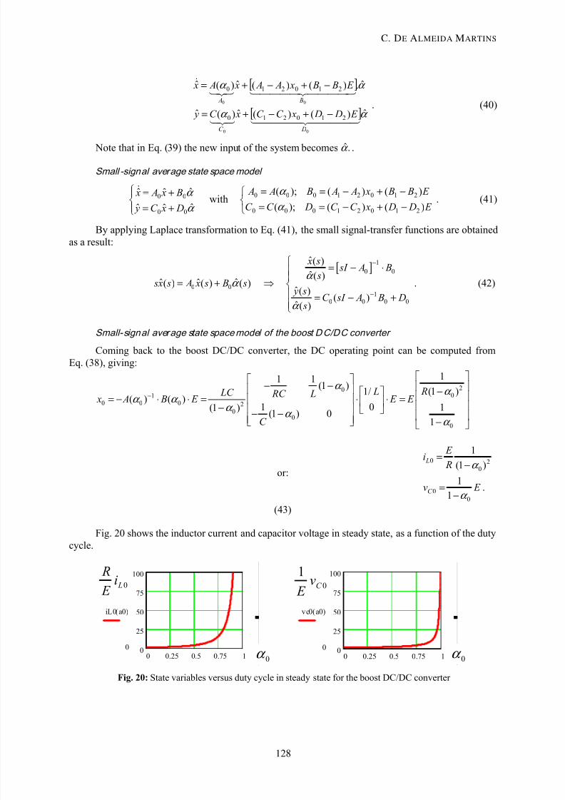
Coming back to the boost DC/DC converter, the DC operating point can be computed from
Eq. (38), giving:
2001
0 0 0 20
0 0
11 1(1 )
(1 )1/( ) ( )
1 0 1(1 )(1 ) 0
1
R L LC RC L x A B E E E
C
α α
α α α
α α
−
⎡ ⎤⎡ ⎤− − ⎢ ⎥⎢ ⎥ −⎡ ⎤ ⎢ ⎥= − ⋅ ⋅ = ⋅ ⋅ =⎢ ⎥ ⎢ ⎥ ⎢ ⎥− ⎢ ⎥ ⎣ ⎦− −
⎢ ⎥⎢ ⎥ −⎣ ⎦ ⎣ ⎦
or:
.1
1
)1(
1
0
0
20
0
E v
R
E i
C
L
α
α
−=
−=
(43)
Fig. 20 shows the inductor current and capacitor voltage in steady state, as a function of the duty
cycle.
0 0.25 0.5 0.75 10
25
50
75
100100
0
iL0 a0( )
0 Li E
R
0α
0 0.25 0.5 0.75 10
25
50
75
100100
0
vc0 a0( )
0
1C v
E
0α
Fig. 20: State variables versus duty cycle in steady state for the boost DC/DC converter
C. DE ALMEIDA MARTINS
128

7/25/2019 Methods for a Systematic Analysis of Power Converters
http://slidepdf.com/reader/full/methods-for-a-systematic-analysis-of-power-converters 27/30
From Eq. (41):
0 0ˆˆ ˆ x A x B α = + with
00
0 0
0 20
110 (1 )
1 ;
11 1(1 ) (1 )
E
L L A B
E
RC C RC
α α
α α
⎡ ⎤⎡ ⎤− − ⎢ ⎥⎢ ⎥ −
⎢ ⎥= =⎢ ⎥⎢ ⎥⎢ ⎥
−− − ⎢ ⎥⎢ ⎥ −⎣ ⎦ ⎣ ⎦
. (44)
Finally, the small signal transfer function, in Laplace, are derived from the first equation of (42):
[ ]0 01
0 02 2
02
0
1 2 1
(1 ) (1 )ˆ( ) 1
1 1ˆ( ) 1(1 ) 1(1 )
E E s
L RCL x s sI A B
s E L s s s RC LC LC R
α α
α α
α
−
⎡ ⎤⎛ ⎞+⎢ ⎥⎜ ⎟
− −⎝ ⎠⎢ ⎥= − ⋅ = ⎢ ⎥
⎛ ⎞+ + − ⎢ ⎥−⎜ ⎟⎜ ⎟⎢ ⎥−⎝ ⎠⎣ ⎦
which gives:
0 0
2 20
1 2 1
ˆ (1 ) (1 )( )
1 1ˆ( )(1 )
L
E E s
L RCLi s
s s s
RC LC
α α
α α
⎛ ⎞+⎜ ⎟
− −⎝ ⎠=
+ + −
and
20
2 20
11
(1 )ˆ ( )
1 1ˆ ( )(1 )
C
E L s
LC Rv s
s s s
RC LC
α
α α
⎛ ⎞−⎜ ⎟
−⎝ ⎠=
+ + −
(45)
6.3 Equivalent average circuit models
Here we present a more straightforward and practical method to derive the state space model. It is an
alternative method which gives, in the cases where it can be applied, the same results as the full
mathematical approach.
This method can be applied only if the following conditions are met:
The time constants of all the state variables in the circuit are significantly higher (approximately 3
times greater) than the switching period.
The duration of all the sequences of the circuit are known and imposed only by the control signals of
the electronic switches. Note that this condition is not met in cases where discontinuous conduction
exists. Indeed, in these cases the duration of the sequence corresponding to the discontinuous
conduction (all switches off) also depends on the values of the state variables. To illustrate this
statement, note that discontinuous conduction often occurs at low inductor current levels but not at
higher levels; thus the duration of this sequence, when it exists, depends on the average current level.
As in state space models obtained by the full mathematical derivation, the dynamic behaviour of all
state variables are not influenced by their harmonic contents at switching frequency and higher terms.This is a consequence of the linear interpolation and averaging illustrated in Fig. 19, which is also
fundamental in this modelling technique.
The principle of the method consists in replacing all the switches in the circuit by equivalent
voltage or current sources in order to obtain an equivalent linear and time-continuous circuit. The
equivalent circuit, free from all electronic switches, can therefore be modelled by any circuit theory
technique and also in particular by state space.
‘Recipe’ to obtain the equivalent average cir cui t
1. Select any sequence of known duration.
2. For that sequence, compute:
METHODS FOR A SYSTEMATIC ANALYSIS OF POWER CONVERTERS
129

7/25/2019 Methods for a Systematic Analysis of Power Converters
http://slidepdf.com/reader/full/methods-for-a-systematic-analysis-of-power-converters 28/30
– the current through all closed switches as a function of state variables and/or source values;
– the voltages across all open switches as a function of state variables and/or source values.
3. Draw an equivalent circuit, by replacing:
–
the closed switches by their current pondered by the existence duration; – the open switches by their voltage sources pondered by the existence duration.
Appli cation to the BOOST converter
By applying the above described ‘recipe’ to the circuit of Fig. 17, choosing sequence 1, the
following equivalent circuit is obtained (Fig. 21):
C R E
L
vC
i L
vC
i L
Sequence 1: - durationα
C R E
L
vC
i L
α vC
- +
α i L
Sequence 1: - durationα
Fig. 21: BOOST DC/DC converter circuit in sequence 1 and equivalent average circuit
The transistor in closed state (see Fig. 17) was replaced by a current source whose value is the
on-state transistor current (iL) multiplied by the sequence existence duration (α ). The diode in open
state (Fig. 17) is replaced by a voltage source whose value is the voltage across it ( vC), again
multiplied by the sequence duration.
The equivalent average circuit can now be easily modelled by the following system of
equations.
LC C
C CL L
d
d.
d
d
i E L v v
t
v vi i C
t R
α
α
⎧= − +⎪⎪
⎨⎪ − = +⎪⎩
(46)
If sequence 2 were chosen instead, the equivalent average circuit would be (Fig. 22):
C R E
L
vC
i L
i L
vC
Sequence 2: - duration(1−α)
C
R E
L
vC
i L
(1 -α )i L
(1 -α )vC
Sequence 2: - du ration(1−α)
| +
Fig. 22: BOOST DC/DC converter circuit in sequence 2 and equivalent average circuit
In this case, the open transistor is replaced by a voltage source with value equal to the voltage
across its terminals multiplied by this sequence existence duration (1– α ). In the same way, the closed
diode is replaced by a current source with value equal to the current flowing through ( iL) multiplied by
the same sequence existence duration.
This equivalent average circuit can also be easily modelled by the system of equations below:
C. DE ALMEIDA MARTINS
130

7/25/2019 Methods for a Systematic Analysis of Power Converters
http://slidepdf.com/reader/full/methods-for-a-systematic-analysis-of-power-converters 29/30
LC
C CL
d(1 )
d
d(1 )
d
i E L v
t
v vi C
t R
α
α
⎧= + −⎪⎪
⎨⎪ − = +⎪⎩
. (47)
Note that the equation systems given by (46) and (47) are identical and can be modelled in state
space by the following state space equation:
LL
CC
10
1/
1 1 0 u
B x x
A
i Li L E
vv
C RC
α
α
−⎡ ⎤−⎢ ⎥⎡ ⎤ ⎡ ⎤ ⎡ ⎤
= +⎢ ⎥⎢ ⎥ ⎢ ⎥ ⎢ ⎥−⎢ ⎥ ⎣ ⎦⎣ ⎦⎣ ⎦ −
⎢ ⎥⎣ ⎦
. (48)
The DC operating point can be computed from Eq. (49):
10 0 0( ) ( ) A B E α α
−= − ⋅ ⋅ ⇒
2L0 0
0
C0
0
1
(1 )
1
1
E
Ri x
v E
α
α
⎡ ⎤
⎢ ⎥−⎡ ⎤ ⎢ ⎥= =⎢ ⎥ ⎢ ⎥⎣ ⎦⎢ ⎥
−⎣ ⎦
. (49)
A small signal model can also be derived by linearization of the state equation around an
operating point:
const E
E) , f(x, x
=
= α ; α
α α α
ˆˆˆ),(),( 0000 x x
f x
x
f x
∂
∂+
∂
∂= ; α
α α
α
ˆˆ)(ˆ
0
0
0
0
)(
0
B A
x A
x A x∂
∂+= ,
or:
00
00
0 20
110 (1 )
(1 )ˆˆ ˆ
11 1(1 )
(1 ) A B
E
L L x x
E
RC C RC
α α
α
α α
⎡ ⎤⎡ ⎤− − ⎢ ⎥⎢ ⎥ −
⎢ ⎥= +⎢ ⎥⎢ ⎥⎢ ⎥ −− − ⎢ ⎥⎢ ⎥ −⎣ ⎦ ⎣ ⎦
. (50)
By applying the Laplace transformation to Eq. (50), the transfer functions between the input
duty cycle and the state variables are obtained:
[ ]1
0 0
ˆ( )
ˆ ( )
x s sI A B
sα
−= − ⋅
0 0L
2 20
1 2 1
ˆ (1 ) (1 )( )
1 1ˆ( )(1 )
E E s
L RCLi s
s s s
RC LC
α α
α α
⎛ ⎞+⎜ ⎟
− −⎝ ⎠=
+ + −
;
20C
2 20
11
(1 )ˆ ( )
1 1ˆ( )(1 )
E L s
LC Rv s
s s s
RC LC
α
α α
⎛ ⎞−⎜ ⎟
−⎝ ⎠=
+ + −
. ( 51 )
The expressions given by (51) are the same as the ones obtained with the state modelling
approach based on the mathematical developments (45).
METHODS FOR A SYSTEMATIC ANALYSIS OF POWER CONVERTERS
131

7/25/2019 Methods for a Systematic Analysis of Power Converters
http://slidepdf.com/reader/full/methods-for-a-systematic-analysis-of-power-converters 30/30
7 Conclusion
The phase plane representation is a straightforward graphical tool for the analysis of power converters
formed by sequences with up-to second-order circuits. The evolution of the state variables (inductor
current and capacitor voltage) within a switching cycle can be easily drawn by following the specific
set of rules described. The corresponding time domain waveforms can also be directly derived.
This graphical tool is used within a sequential analytical method of study, in which the power
converter circuit is decomposed into different sequences, each one corresponding to one configuration
of states of the electronic switches. In each sequence, the state variables evolution in the phase plane is
derived and the conditions for transition to another sequence are evaluated. By following the specified
flowchart, any power converter can be analysed in a systematic approach, avoiding dead-locks and
turn-arounds in the study flow and being sure that all possible sequences are considered.
Two modelling techniques of power converters are presented: the first one, more general, is
based on mathematical developments in the state space domain; the second one, more direct and
practical, in which a linear and time-continuous equivalent average circuit is drawn. The validity
assumptions of both techniques are presented and discussed.
Acknowledgements
The author would like to express his deep gratitude to the researchers of the LEEI laboratory, in
Toulouse, France, who have been engaged throughout the last 20 years in the preparation and
consolidation of the methods of study of power converters presented here. The author would like to
thank in particular Dr Thierry Meynard and Dr Michel Metz for their support in the preparation of this
document.
Bibliography
Y. Cheron, T. Meynard and C. Goodman, Soft Commutation (Chapman & Hall, 1992).
Y. Cheron, La commutation douce dans la conversion statique de l’energie electrique (Technique et
Documentation Lavoisier, 1989) (in French).
Foch et al., Méthodes d’études des convertisseurs statiques, Lecture notes in Power Electronics
(ENSEEIHT, Institut National Polytechnique de Toulouse, April 1988) (in French).
K. Ogata, Modern Control Engineering, 4th edition (Prentice Hall, 2001).
C. DE ALMEIDA MARTINS