Embed Size (px)
Citation preview

800.0117
METHODS AND APPARATUS FOR SINGLE STAGE GALOIS FIELD OPERATIONS
Field of the Invention
The present invention relates generally to improvements to digital signal processing and
more particularly to advantageous methods and apparatus for providing improved Galois field
operations.
Background of the Invention
The operations of addition and multiplication utilizing Galois field (GF) arithmetic are
very different from the usual multiply and add instructions in digital signal processors (DSPs).
Specialized instructions are therefore typically needed to perform the computations in a
reasonable amount of time. The specialized instructions specify the inputs, the result destination
and the type of GF operation to be executed. A GF multiplication operation of two input
elements is an important function which signal processing units and DSPs may need to perform.
In considering GF operations, there are at least two different ways to encode the elements of a
GF: 1) using the polynomial coefficients as a vector of bits, or 2) using the exponent form. Both
of these two encodings make the calculation of one of the operations easy, but the other more
complex to calculate. For example, the GF addition in utilizing the polynomial coefficients
approach is an exclusive or (XOR), while a multiplication of two elements in exponent form is
an addition of the exponents. However, the multiplication operation, utilizing the polynomial
coefficient form, and, the addition operation, utilizing the exponent form, are typically both
more complex to implement.
1

Further details of several prior art approaches are found in the following patents: “Galois
Field Computer,” U.S. Patent No. 4,162,480, “Multiplier in a Galois Field,” U.S. Patent No.
4,918,638, and “Galois Field Arithmetic Apparatus and Method,” U.S. Patent No. 6,134,572.
The first patent describes a table lookup for the GF multiplication of GF(25). The second patent
uses two function stages to calculate a GF multiplication utilizing a binary multiplier array for a
first function stage and a polynomial reducer for the second function stage. The third patent uses
the exponent representation form.
Summary of the Invention
Galois fields (GF) and the multiplication operation in such fields, have many applications
in communication systems. Some examples are their utilization for error detection and/or
correction, for cryptography, and the like. Due to the special meaning of GF multiplication,
however, standard signal processors typically are inefficient in performing such a computation.
It is therefore important to consider techniques and designs to efficiently compute the operations
needed in a signal processor, such as a DSP or a fixed function signal processor, over different
Galois extension fields and generator polynomials. The present invention advantageously
calculates the GF multiplication in polynomial coefficients form as a single function stage
calculation by merging two function stages into a single new function stage. The new single
function stage GF(2m) multiplication further advantageously uses an m-by-m single function
stage calculation array utilizing only m-bits per internal logic stage as compared with the
previous two function stage approach of U.S. Patent No. 4,918,638, which calculated 2m-1 bits
from the first stage multiplication array as inputs to the second stage polynomial reducer. The
present invention provides a savings of m-1 bits per logic stage that do not need to be accounted
for in the internal array implementation. One regular m-by-m array in accordance with the
2

invention may be constructed by replicating a common cell circuit design allowing for futher
optimizations, for example, using custom logic design techniques to produce a common cell that
is of higher performance and reduced area. In addition, the GF multiplication array can be
physically instantiated multiple times and used by DSP software programs with a specialized
instruction to perform multiple GF multiplications on multiple data elements in a packed data
format. For parallel DSPs with multiple processing elements (PEs), the specialized instruction
can be used in programs to perform the packed data format GF multiplications on the multiple
PEs in parallel.
These and other advantages and aspects of the present invention will be apparent from the
drawings and the Detailed Description which follow below.
Brief Description of the Drawings
Fig. 1A illustrates a first function stage for computing polynomial multiplication terms in
a traditional two function stage GF multiplication approach showing exemplary calculation
traces for two polynomial multiplications;
Figs. 1B and 1C illustrate the first function stage polynomial multiplications as if done by
hand for the two examples of Fig. 1A;
Fig. 2 illustrates a second function stage for performing polynomial division in a
traditional two function stage approach showing two reductions of the two dividends from Fig.
1A to generate two remainders which are the result of the GF multiplications;
Fig. 3A illustrates a first logic stage with i=1 calculating Y(1) for m=3 in accordance
with the present invention;
3

Fig. 3B illustrates first and second logic stages with i=2 calculating Y(2) for m=3 in
accordance with the present invention;
Fig. 3C illustrates first, second and third logic stages with i=3 calculating Y(3), the GF
multiplication result, for m=3 in accordance with the present invention;
Fig. 4 illustrates a GF multiplication cell for construction of an m-by-m GF multiplication
array in accordance with the present invention;
Fig. 5 illustrates a single m=8 GF multiplication unit which may suitably be used in a
ManArray architecture processor in accordance with the present invention;
Fig. 6 illustrates a Manta-type processor, a subset of the ManArray architecture, which
may be suitably adapted for use in conjunction with the present invention;
Fig. 7A illustrates an exemplary encoding format for a packed data finite field multiply
instruction (MPYGF) in accordance with the present invention; and
Fig. 7B shows a syntax/operation table for the MPYGF instruction of Fig. 7A.
Detailed Description
To provide context for a hardware implementation, and instructions and software
techniques for GF multiplication in accordance with the present invention, a brief description of
GF arithmetic follows below. A field F(S,+,*,0,1) defines an algebraic entity consisting of a set
of elements S, two arithmetic operations, addition and multiplication, denoted by the symbols +
and *, respectively, closed over S and the corresponding identity elements for these operations,
denoted by 0 and 1, respectively. A Galois field is a defined subset of a general field which is a
set, such as the set of rational numbers, that can be manipulated by the mathematical operations
of addition and multiplication. A Galois field is represented as GF(q) where q represents the
finite number of elements of the field, for this case the integers {0,1, … , q-1}. For example, let
4

q=2 such that GF(2) has elements {0,1}. An extension field of interest is GF(2m) where m is a
positive integer. This Galois field has 2m elements of the vector space of dimension m over
GF(2). It has been proven that every finite field is isomorphic to a Galois field. Also, any field
GF(2m) can be generated using a primitive polynomial P of degree m over GF(2), and the
arithmetic performed in the GF(2m) field is modulo this primitive polynomial.
A traditional implementation of GF multiplication consists of two function stages, which
perform the GF multiplication much as it would be computed by hand. For further exemplary
details of such an implementation, see U.S. Patent No. 4,918,638. During a first function stage, a
polynomial multiplication is implemented, where the polynomials have coefficients from GF[2].
This operation is a modification of a typical multiplier where the carries are not calculated or
propagated. In the second function stage, the corresponding polynomial division by the
generator polynomial is implemented where the remainder is calculated as discussed further
below.
The GF multiplication can be derived as follows: let g[x] be the generator polynomial of
GF[2m]. Let polynomials p[x] and q[x] be members of GF[2m] / g[x]. The GF multiplication is
the calculation of the remainder of the polynomial division of the product p[x]*q[x] divided by
g[x] in GF[2] arithmetic. It is noted that a polynomial with coefficients in GF[2] multiplied by
the monomial xm is equivalent to shifting the bit vector of the polynomial coefficients to the left
m positions with zero fill in. Polynomial addition is equivalent to performing a bit wise
exclusive or (XOR) operation. Also, note that subscripts represent a specific bit position in a bit
vector, the asterisk symbol (*) represents bit ANDs, and the symbols + and ⊕ represent the XOR
operation.
5

Polynomial multiplication may be calculated by a recurrence relation equation 1 that
defines the polynomial S(i) :
S(i) = S(i-1) + qm-i* p * xm-i , for i = 1...m, and where S(0) = 0 Equation 1
where S(m) is the polynomial product of p[x]*q[x]. For example, Fig. 1A shows a first stage
polynomial multiplication table 100 with equation 1 multiplication terms 102 and calculation
results 104 and 106 for a common input p=(p4 p3 p2 p1 p0) and two different inputs q=(q4 q3 q2 q1
q0) for m=5. For calculation results 104, p=11101 and q=10111. For calculation results 106,
p=11101 and q=10010. Figs. 1B and 1C show multiplication operations 150 and 170 for the two
examples 104 and 106, respectively, of Fig. 1A as if done by hand.
The polynomial remainder of the division of p[x]*q[x] divided by g[x] is calculated by
the recurrence relation equation that defines the polynomial Z(i) :
Z(i) = Z(i-1) + Z(i-1)2m-i* g * xm-i , for i = 2...m, and where Z(1) = S(m) Equation 2
The remainder is given by the least significant m-bits of Z(m).
In one traditional approach to GF multiplication in which polynomial multiplication is
followed by a polynomial division, the result of the multiplication becomes the dividend for the
reduction operation. For example, Fig. 2 illustrates a second polynomial division stage reduction
operation 200 where remainder terms 202 and division operations 204 and 206 continue the
examples shown in Fig. 1A. The generator polynomial is g(x) = x5 + x2 + 1, that is, the
coefficients of the divisor are given in binary form as (100101) . For the first example of a
division operation 204, the binary dividend (110000011) 210 corresponds to the polynomial x8 +
x7 + x + 1. In the other example of a division operation 206, the binary dividend (111101010)
212 corresponds to the polynomial x8 + x7 + x6 + x5 + x3 + x .
Returning to Fig. 1A, the equation 1 multiplication terms 102 with m=5, are as follows:
6

S(0)=0 107
S(1) = S(0) + q4*p*x4 = q4*p*x4 108
S(2) = S(1) + q3*p*x3 = q4*p*x4 + q3*p*x3 109
S(3) = S(2) + q2*p*x2 = q4*p*x4 + q3*p*x3 + q2*p*x2 110
S(4) = S(3) + q1*p*x1 = q4*p*x4 + q3*p*x3 + q2*p*x2 + q1*p*x1 111
S(m) = S(5) = S(4) + q0*p*x0 = q4*p*x4 + q3*p*x3 + q2*p*x2 + q1*p*x1+ q0*p*x0 112
The exemplary multiplication operations shown in Figs. 1B and 1C include reference numbers
corresponding to those in the calculation result columns 104 and 106 of Fig. 1A. Note that
equation 1 generates 2m-1 bits, as can be seen for the result S(5) 112 and the examples 150 and
170. Thus, the results 135 and 136 have 2(5)-1 or 9 bits. It is further noted that for GF
multiplication, the carries are not calculated or propagated.
Next equation 2 is discussed with reference numbers included in the equation steps
corresponding to the rows of the exemplary calculations shown in Fig. 2. Fig. 2 shows
remainder terms 202, calculation results 204 for p=11101, q=10111 and g=10010, and
calculation results 206 for p=11101, q=10010 and g=10010. For m=5 and i=1, the first term
Z(1) is defined as:
Z(1) = S(m) = S(5) 208
For i=2, the next term Z(2) is:
Z(2) = Z(1) + Z(1)8*g*x3 214
For i=3, the next term Z(3) is:
Z(3) = Z(2) + Z(2)7*g*x2 220
For i=4, the next term Z(4) is:
Z(4) = Z(3) + Z(3)6*g*x1 226
7

For i=5, the next term Z(5) is:
Z(5) = Z(4) + Z(4) 5*g*x0 232
For calculation results of the division operations 204 and 206 of Fig. 2, equation 2
specifies the remainders, and thus the GF products 240 and 242, which are (11010) and (11100),
respectively. The first GF product 240 corresponds to x4+x3+x and the second GF product 242
corresponds to x4+x3+x2 . Note that the calculation of equation 2 requires the use of 2m-1 bits as
shown in each calculation step in the table 200 calculation results columns 204 and 206.
With the above discussion of Figs. 1A, 1B and 2 as background, it is next shown how the
present invention computes the GF multiplication in a single new function stage. In the approach
of the present invention, equation 2 is expanded by incorporating the input Z(1)=S(m) terms and
combining the terms in the equation in such a way as to create a new and different recurrence
relation that represents a single function stage calculation of a GF(2m) multiplication.
For m=5 and i=1, the first term Z(1) is defined as:
Z(1) = S(m) = S(5) = q4*p*x4 + q3*p*x3 + q2*p*x2 + q1*p*x1+ q0*p*x0
Using equation 2 and i=2, the next term Z(2) can be written as:
Z(2) = Z(1) + Z(1)8*g*x3
Substituting for Z(1) leads to:
Z(2) = q4*p*x4 + q3*p*x3 + q2*p*x2 + q1*p*x1+ q0*p*x0+ Z(1)8*g*x3
Combining the common x3 terms of the input S(5), q3*p*x3, with the division recurrence term,
Z(1)8*g*x3, changes the nature of the equation being evaluated as can be seen in the following
steps and discussed further below. The Z(2) term using combined input terms is:
Z(2) = q4*p*x4 + (q3*p + Z(1)8*g)*x3 + q2*p*x2+ q1*p*x1+ q0*p*x0
Using equation 2 and i=3, the next term Z(3) can be written as:
8

Z(3) = Z(2) + Z(2)7*g*x2
Substituting for Z(2) leads to:
Z(3) = q4*p*x4 + (q3*p + Z(1)8*g)*x3 + q2*p*x2 + q1*p*x1+ q0*p*x0+ Z(2)7*g*x2
Combining the common x2 terms of the input S(5), q2*p*x2, with the division recurrence term,
Z(2)7*g*x2, yields:
Z(3) = q4*p*x4 + (q3*p + Z(1)8*g)*x3 + (q2*p + Z(2)7*g)*x2 + q1*p*x1+ q0*p*x0
Using equation 2 and i=4, the next term Z(4) can be written as:
Z(4) = Z(3) + Z(3)6*g*x1
Substituting for Z(3) leads to:
Z(4) = q4*p*x4 + (q3*p + Z(1)8*g)*x3 + (q2*p + Z(2)7*g)*x2 + q1*p*x1+ q0*p*x0 + Z(3)6*g*x1
Combining the common x1 terms of the input S(5), q1*p*x1, with the division recurrence term,
Z(3)6*g*x1, yields:
Z(4) = q4*p*x4 + (q3*p + Z(1)8*g)*x3 + (q2*p + Z(2)7*g)*x2 + (q1*p + Z(3)6*g) *x1 + q0*p*x0
Using equation 2 and i=5, the next term Z(5) can be written as:
Z(5) = Z(4) + Z(4) 5*g*x0
Substituting for Z(4) leads to:
Z(5) = q4*p*x4 + (q3*p + Z(1)8*g)*x3 + (q2*p + Z(2)7*g)*x2 + (q1*p + Z(3)6*g) *x1 +
q0*p*x0 +Z(4) 5*g*x0
Combining the common x0 terms of the input S(5), q0*p*x0, with the division recurrence term,
Z(4) 5*g*x0, yields:
Z(5) = q4*p*x4 + (q3*p + Z(1)8*g)*x3 + (q2*p + Z(2)7*g)*x2 + (q1*p + Z(3)6*g) *x1 +
(q0*p+ Z(4) 5*g) *x0 Equation 3
9

Due to the combining of the common input terms with the division recurrence terms,
equation 3 represents a new recurrence relation that can be written in a general form as follows:
Y(i) = Y(i-1) + (qm-i*p + Y(i-1)2m-i*g)*xm-i , i=1, 2, …, m and where Y(0) = 0 Equation 4
Note that Y(m) = Z(m) but, because of the combining of the terms as described above, Y(a) ≠
Z(a) when a<m. The intermediate terms Y(a) are not output results and the final answer Y(m) is
all that is needed. Equation 4 can be implemented as an advantageous merging of the two
previously separate function stages into a single function stage that is represented by the new
recurrence relation equation 4. As indicated by Equation 4, there is no inherent algorithmic
limitation to handling arbitrary values of m with the approach of the present invention.
Equation 4 can be simplified further by examining the Y(i-1)2m-i term by first specifying i
as i-1 and then substituting i-1 into Equation 4 for the purpose of determining the 2m-i bit.
Y(i-1)2m-i = (Y(i-2) + (qm-(i-1)*p + Y(i-2)2m-(i-1)*g)*xm-(i-1) )2m-i , which is valid for i=2, 3, …, m
and where Y(0) = 0. Because polynomial addition is equivalent to performing a bit wise
exclusive or operation with no carries calculated, a bit of a vector exclusive or result is equal to
the exclusive or of the input bits. Thus:
Y(i-1)2m-i = Y(i-2)2m-i + ((qm-(i-1)*p + Y(i-2)2m-(i-1)*g)*xm-(i-1) )2m-i .
As noted earlier, a polynomial with coefficients in GF[2] multiplied by the monomial xm
is equivalent to shifting the bit vector of the polynomial coefficients to the left m positions with
zero fill in. Consequently, a bit represented by (A* xm-(i-1))2m-i is equivalent to A2m-i-(m-(i-1))=Am-1.
Therefore, Y(i-1)2m-i = Y(i-2)2m-i + (qm-i+1*p + Y(i-2)2m-i+1*g)2m-i – (m-(i-1)) and simplifying yields:
Y(i-1)2m-i = Y(i-2)2m-i + (qm-i+1*p + Y(i-2)2m-i+1*g)m-1 Equation 5
which is valid for i=2, 3, …, m and where Y(0) = 0.
10
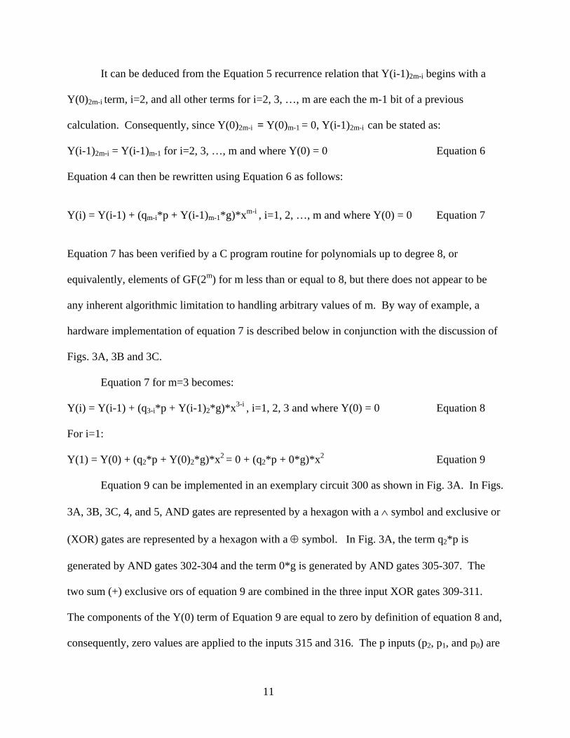
It can be deduced from the Equation 5 recurrence relation that Y(i-1)2m-i begins with a
Y(0)2m-i term, i=2, and all other terms for i=2, 3, …, m are each the m-1 bit of a previous
calculation. Consequently, since Y(0)2m-i = Y(0)m-1 = 0, Y(i-1)2m-i can be stated as:
Y(i-1)2m-i = Y(i-1)m-1 for i=2, 3, …, m and where Y(0) = 0 Equation 6
Equation 4 can then be rewritten using Equation 6 as follows:
Y(i) = Y(i-1) + (qm-i*p + Y(i-1)m-1*g)*xm-i , i=1, 2, …, m and where Y(0) = 0 Equation 7
Equation 7 has been verified by a C program routine for polynomials up to degree 8, or
equivalently, elements of GF(2m) for m less than or equal to 8, but there does not appear to be
any inherent algorithmic limitation to handling arbitrary values of m. By way of example, a
hardware implementation of equation 7 is described below in conjunction with the discussion of
Figs. 3A, 3B and 3C.
Equation 7 for m=3 becomes:
Y(i) = Y(i-1) + (q3-i*p + Y(i-1)2*g)*x3-i , i=1, 2, 3 and where Y(0) = 0 Equation 8
For i=1:
Y(1) = Y(0) + (q2*p + Y(0)2*g)*x2 = 0 + (q2*p + 0*g)*x2 Equation 9
Equation 9 can be implemented in an exemplary circuit 300 as shown in Fig. 3A. In Figs.
3A, 3B, 3C, 4, and 5, AND gates are represented by a hexagon with a ∧ symbol and exclusive or
(XOR) gates are represented by a hexagon with a ⊕ symbol. In Fig. 3A, the term q2*p is
generated by AND gates 302-304 and the term 0*g is generated by AND gates 305-307. The
two sum (+) exclusive ors of equation 9 are combined in the three input XOR gates 309-311.
The components of the Y(0) term of Equation 9 are equal to zero by definition of equation 8 and,
consequently, zero values are applied to the inputs 315 and 316. The p inputs (p2, p1, and p0) are
11

applied to inputs 317, 318 and 319, respectively, and the generator polynomial coefficients g
inputs (g2, g1, and g0) are applied to inputs 320, 321 and 322, respectively. The input Y(0)2=0 is
provided on input 323, a zero is provided on input 324 being at the edge of the array, and q2 is
provided on input 325. The results Y(1)2 , Y(1)1 , and Y(1)0 of circuit 300 appear at outputs 326,
327, and 328, respectively. To allow the use of a common cell for implementing the array, a
third XOR input on border cells, such as input 324 of cell 329 is set to zero.
Continuing for i=2:
Y(2) = Y(1) + (q1*p + Y(1)2*g)*x1 = (q2*p + 0*g)*x2 + (q1*p + Y(1)2*g)*x1 Equation 10
Equation 10 can be implemented in an exemplary circuit 330 as shown in Fig. 3B. In Fig. 3B,
the term q1*p = q1 331 * (p2 317 p1 318 p0 319) is generated by AND gates 332-336 and the term
Y(1)2*g = Y(1)2 326 * (g2 320 g1 321 g0 322) is generated by AND gates 340-344. The two
required sum (+) exclusive ors are combined in the three input XOR gates 350-354. Note that
due to the x2 and x1 terms in Equation 10, there is a shift of 1 bit in the exclusive or inputs
accounting for paths 327 and 328 for Y(1)1 and Y(1)0, respectively. Border cell 355 has its
XOR third input 356 set to zero. The results of circuit 330 are outputs Y(2)2 357, Y(2)1 358, and
Y(2)0 359.
Continuing for i=3:
Y(3) = Y(2) + (q0*p + Y(2)2*g)*x0
Y(3) = (q2*p + 0*g)*x2 + (q1*p + Y(1)2*g)*x1 + (q0*p + Y(2)2*g)*x0 Equation11
Equation 11 can be implemented in an exemplary circuit 360 shown in Fig. 3C where the term
q0*p = q0 361 * (p2 317 p1 318 p0 319) is generated by AND gates 372-376 and the term Y(2)2*g
= Y(2)2 357 * (g2 320 g1 321 g0 322) is generated by AND gates 380-384. The two required sum
(+) exclusive ors are combined in the three input XOR gates 390-392. Note that due to the x0
12

term in Equation 11 there is a shift of 1 bit in the exclusive or inputs accounting for paths 358
and 359 for Y(2)1 and Y(2)0, respectively. Border cell 395 has its XOR third input 396 set to
zero. The results of circuit 360 are outputs Y(3)2 397, Y(3)1 398, and Y(3)0 399.
It is noted that the above described implementation of equation 7 requires only m bits for
each logic stage, as shown in the exemplary circuits of Fig. 3A, 3B, and 3C. By contrast, the
previous calculation techniques for the examples of Figs. 1A-1C and Fig. 2 required 2m-1 bits
per logic stage. This reduction represents a savings of m-1 bits per internal logic stage that do
not have to be accounted for in an implementation.
Fig. 4 illustrates a GF multiplication cell 400 where cell output bit Y(i)j 402 depends on
the most significant bit of the previous calculation Y(i-1)m-1 404, the value of its right neighbor
bit Y(i-1)j-1 406 the result of the previous calculation, bit qm-i 408, bit pj 410, and bit gj 412.
Internal to the GF multiplication cell 400 are two 2-input AND gates 414 and 416 and a 3-input
XOR gate 418. The three logic gates are connected based on Equation 7, repeated here for easy
reference to the logic gates of Fig. 4, Y(i) = Y(i-1) + (qm-i*p + Y(i-1)m-1*g)*xm-i . The qm-i*p
AND is accomplished for the jth bit position by AND gate 414, the Y(i-1)m-1*g AND for the jth
bit position is accomplished by the AND gate 416, the XOR of these two AND results is
accomplished by XOR gate 418. The third input 406 to the XOR gate 418 is for the Y(i-1) j-1
term, which, due to the xm-i term of equation 7, has a shift of one bit between the previous Y(i-1)
value and the (qm-i*p + Y(i-1)m-1*g) value. This one-bit shift is accomplished for the bit position
Y(i)j 402 by XOR 418 having its third input being the previous Y term shifted by 1 bit, in other
words bit Y(i-1)j-1 406.
Note that for border cells on the rightmost edge of a GF multiplication array, for
example, cells 329, 355 and 395 as shown in Fig. 3C, the third XOR inputs, 324, 356, and 396,
13

respectively, are set to zero. The same is true for input 406 in general cell 400 when the cell is
used as a border cell on the rightmost edge of a GF multiplication array. A regular m-by-m
array is constructed by replicating a common cell circuit design, such as circuit 400 of Fig. 4,
allowing for futher optimizations, for example, using custom logic design techniques to produce
a common cell that is of higher performance and reduced area.
A single exemplary m=8 GF multiplication unit 500 is shown in Fig. 5. Unit 500 consists
of an m-by-m=8x8 array of the GF cells 400 shown in Fig. 4. The inputs q = (q7 q6 q5 q4 q3 q2 q1
q0) 504, p = (p7 p6 p5 p4 p3 p2 p1 p0) 508, g = (g7 g6 g5 g4 g3 g2 g1 g0) 512 are provided from an
external source such as the read ports of at least two registers or a register file or memory device.
The Y(i-1)m-1 and the Y(i-1)j-1 array border GF multiplication circuit cell input values 516 and
520 are set to 0. The result Y = (Y(8)7 Y(8)6 Y(8)5 Y(8)4 Y(8)3 Y(8)2 Y(8)1 Y(8)0) output 524 is
provided to an external destination such as the write port of a register or a register file or memory
device.
The present invention computes the GF multiplication in a single stage. In one
implementation, it may be embodied as an instruction for the MANARRAYTM architecture
wherein 8 GF multipliers are incorporated in each processing element. This arrangement allows
a GF multiplication instruction, as described in more detail below, using the same generator
polynomial for each GF multiplication, to cause 8 GF multiplications to be calculated
simultaneously on each processing element by using 8 GF multiplication units 500. The GF
multiplication instruction implemented for the MANARRAY™ architecture accomplishes the 8
GF multiplications by operating on packed data of 8 bytes producing 8 results on each
processing element every cycle. With a four PE array, 32 GF multiplications can be obtained
each cycle. For reasons of programming flexibility, the GF multiplication instruction also
14

specifies 4 GF multiplications for operation on 4 bytes packed in 32-bit words and 8 GF
multiplications for operations on 8 bytes packed in 64-bit double words.
More specifically and in an illustrative embodiment of the present invention, an
exemplary ManArray 2x2 iVLIW single instruction multiple data stream (SIMD) processor 600,
representative of the Manta processor and mobile media processor (MMP) which are both
subsets of the ManArray architecture, as shown in Fig. 6, may be adapted as described further
below for use in conjunction with the present invention. Processor 600 comprises a sequence
processor (SP) controller combined with a processing element-0 (PE0) to form an SP/PE0
combined unit 601, as described in further detail in U.S. Patent No. 6,219,776. Three additional
PEs 651, 653, and 655 are also labeled with their matrix positions as shown in parentheses for
PE0 (PE00) 601, PE1 (PE01)651, PE2 (PE10) 653, and PE3 (PE11) 655. The SP/PE0 601
contains an instruction fetch (I-fetch) controller 603 to allow the fetching of “short” instruction
words (SIW) or abbreviated- instruction words from a B-bit instruction memory 605, where B is
determined by the application instruction-abbreviation process to be a reduced number of bits
representing ManArray native instructions. If an instruction abbreviation apparatus is not used,
then B is determined by the SIW format.
The fetch controller 603 provides the typical functions needed in a programmable
processor, such as a program counter (PC), a branch capability, and eventpoint loop operations.
It also provides the instruction memory control which could include an instruction cache if
needed by an application. In addition, the I-fetch controller 603 controls the dispatch of
instruction words, such as a GF multiplication instruction, and instruction control information to
the other PEs in the system by means of a D-bit instruction bus 602. D is determined by the
implementation taking into account the SIW format, which for the exemplary ManArray
15

coprocessor D=32-bits. The instruction bus 602 may include additional control signals as needed
to distribute instructions to the multiple processing elements.
In this exemplary system 600, common elements are used throughout to simplify the
explanation, though actual implementations are not limited to this restriction. For example, the
execution units 631 in the combined SP/PE0 601 can be separated into a set of execution units
optimized for the control functions of the SP. Fixed point execution units can be used in the SP,
while PE0 and the other PEs can be optimized for a floating point application. For the purposes
of this description, it is assumed that the execution units 631 are of the same type in the SP/PE0
and the PEs. The MAU execution units 632, 633, 634 and 635 each contain eight GF
multiplication units, each of the type 500 shown in Fig. 5, for GF multiplication instruction
execution capability. The MAUs provide the GF multiplication units with register file access
interfaces. Each of the register files contained in the SP/PE0 and the other PEs are a common
design PE configurable register file, 611, 627, 627', 627'', and 627''', which is described in further
detail in U.S. Patent No. 6,343,356.
The SP/PE0 and the other PEs use a five instruction slot indirect very long instruction
word (iVLIW) architecture which contains a VLIW instruction memory (VIM) 609 and an
instruction decode and VIM controller functional unit 607 which receives instructions as
dispatched from the SP/PE0’s I-fetch unit 603 and generates VIM addresses and control signals
608 required to access the iVLIWs stored in the VIM. Referenced instruction types are
identified by the letters SLAMD in VIM 609, where the letters are matched up with instruction
types as follows: Store (S), Load (L), ALU (A), MAU (M), and DSU (D). The basic concept of
loading the iVLIWs is described in further detail in U.S. Patent No. 6,151,668. A VLIW, which
may contain a GF multiplication instruction in the MAU slot position, may be indirectly
16
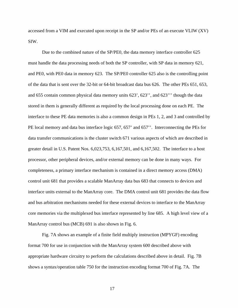
accessed from a VIM and executed upon receipt in the SP and/or PEs of an execute VLIW (XV)
SIW.
Due to the combined nature of the SP/PE0, the data memory interface controller 625
must handle the data processing needs of both the SP controller, with SP data in memory 621,
and PE0, with PE0 data in memory 623. The SP/PE0 controller 625 also is the controlling point
of the data that is sent over the 32-bit or 64-bit broadcast data bus 626. The other PEs 651, 653,
and 655 contain common physical data memory units 623’, 623’’, and 623’’’ though the data
stored in them is generally different as required by the local processing done on each PE. The
interface to these PE data memories is also a common design in PEs 1, 2, and 3 and controlled by
PE local memory and data bus interface logic 657, 657’ and 657’’. Interconnecting the PEs for
data transfer communications is the cluster switch 671 various aspects of which are described in
greater detail in U.S. Patent Nos. 6,023,753, 6,167,501, and 6,167,502. The interface to a host
processor, other peripheral devices, and/or external memory can be done in many ways. For
completeness, a primary interface mechanism is contained in a direct memory access (DMA)
control unit 681 that provides a scalable ManArray data bus 683 that connects to devices and
interface units external to the ManArray core. The DMA control unit 681 provides the data flow
and bus arbitration mechanisms needed for these external devices to interface to the ManArray
core memories via the multiplexed bus interface represented by line 685. A high level view of a
ManArray control bus (MCB) 691 is also shown in Fig. 6.
Fig. 7A shows an example of a finite field multiply instruction (MPYGF) encoding
format 700 for use in conjunction with the ManArray system 600 described above with
appropriate hardware circuitry to perform the calculations described above in detail. Fig. 7B
shows a syntax/operation table 750 for the instruction encoding format 700 of Fig. 7A. The
17

MPYGF instruction 700 calculates the remainder of the polynomial division of the product of
two polynomials with coefficients from Galois field GF[2]. Four GF multiplications can be
specified and calculated simultaneously as shown in syntax/operations description 752 and eight
GF multiplications can be specified and calculated simultaneously as shown in
syntax/operations description 754. The input polynomial coefficients are represented as bits in 4,
or 8, unsigned bytes in source 32-bit registers Rx and Ry or 64-bit register pairs Rxe-Rxo, and
pair Rye-Ryo, respectively. The results of the GF multiplication are stored in the corresponding
bytes of register Rt, or Rte-Rto, respectively. The arithmetic scalar flags (ASFs), representing
possible side effects of the MPYGF operation, are affected only by the least significant sub-
operation of a packed data operation. The C, N and V flags are not affected by the least
significant sub-operation while the Z flag is set to a 1 if the least significant sub-operation is a
zero. Otherwise the Z flag is 0. The MPYGF instruction is defined to take 1 execution cycle.
A polynomial setup register (PSR) located in a register in a miscellaneous register file
(MRF) extension 1 defined in the ManArray architecture to contain the generator polynomial
(PSR.B0) and degree (PSR.B1) of the finite field, with the polynomial coefficients set as bits of
byte PSR.B0. The generator polynomial must be loaded into the PSR using either a Load or a
DSU instruction. Note that m cannot exceed 8 for this instruction due to the present hardware
specification, but, as shown by Equation 7, there does not appear to be any algorithmic
limitation to handling arbitrary values of m.
By way of example, to calculate sixteen GF(25) multiplications of unsigned bytes stored
in the compute register file registers Rx.B0 times Ry.B0 in a four PE system such as shown in
Fig. 6, in the field generated by the generator polynomial g(x) = x5 + x2 + 1, a program first loads
the PSR byte 0 and byte 1 with the generator coefficients and m respectively, and then issues the
18

mpygf instruction, mpygf.sm.4ub Rt, Rx, Ry to all four PEs. When the instruction is executed,
four sets of m-bit results are stored in register file target register Rt in each PE. For example,
one of the calculations in one of the PEs that executes the mpygf.sm.4ub Rt, Rx, Ry instruction
could be Rx.B0=(11101) times Ry.B0=(10111) producing the result (11010) which is stored in
the register file target register Rt.B0 755. Note that three other mpygf operations 757 also occur
in parallel on this PE as specified by the quad operation mpygf instruction 700 and a total of
sixteen GF multiplications occur in parallel on all four PEs.
A program or programs, that emulate a GF multiplication or use a GF multiplication
instruction based on the principles of the present invention, can be stored in an electronic form
on a computer useable medium which can include diskettes, CD-ROM, DVD-ROM, storage on a
hard drive, storage in a memory device using random access memory, flash memory, Read Only
Memory or the like, in downloadable form for downloading through an electronic transport
medium, and the like.
While the present invention has been disclosed in the context of various aspects of
presently preferred embodiments, it will be recognized that the invention may be suitably applied
to other environments and applications consistent with the claims which follow.
19

We claim:
1. A method for Galois field (GF(2m)) multiplication, where m is a positive integer,
and the GF(2m) multiplication operation calculates the multiplication of two polynomials
producing a product which is divided by a generator polynomial, and wherein the multiplication
operation is further combined with the division operation whereby the GF(2m) multiplication
may be computed in a single logic stage, the method comprising:
generating xm-i polynomial coefficient terms from multiplication and division
operations, where i is a variable;
combining like xm-i polynomial coefficient terms from the multiplication and
division operations; and
computing a recurrence relation using the combined xm-i polynomial
coefficient terms for the single GF(2m) multiplication function.
2. The method of claim 1 wherein the recurrence relation for a single GF(2m)
multiplication function is Y(i) = Y(i-1) + (qm-i*p + Y(i-1)2m-1*g)*xm-i , i=1, 2, …, m and where
Y(0) = 0.
3. The method of claim 1 further comprising:
outputting results from computing the recurrence relation; and
storing the results in computer readable form.
4. A method for Galois field (GF(2m)) multiplication, where m is a positive integer,
and the GF(2m) multiplication operation calculates the multiplication of two polynomials
producing a product which is divided by a generator polynomial, and wherein the multiplication
20

operation is further combined with the division operation whereby the GF(2m) multiplication
may be computed in a single logic stage, the method comprising:
generating xm-i polynomial coefficient terms from multiplication and division
operations, where i is a variable;
combining like xm-i polynomial coefficient terms from the multiplication and
division operations; and
computing a simplified recurrence relation using the combined xm-i
polynomial coefficient terms for the single GF(2m) multiplication function thereby calculating m
by m bits for the simplified GF(2m) multiplication function.
5. The method claim 4 wherein the simplified the recurrence relation for the single
GF(2m) multiplication function is Y(i) = Y(i-1) + (qm-i*p + Y(i-1)m-1*g)*xm-i , i=1, 2, …, m and
where Y(0) = 0.
6. The method of claim 4 further comprising:
outputting results from computing the simplified recurrence relation; and
storing the results in computer readable form.
7. A GF multiplication circuit cell producing result Y(i)j for i ∈ {1, 2, …, m}, j ∈ {0,
1, …, m-1}, where m is a positive integer, and a selected i and j value comprising:
a bit qm-i selected from the set {qm-1, qm-2, …, qm-i, …, q0} of first product
inputs;
a bit pj selected from the set {pm-1, pm-2, …, pj, …, p0}of second product
inputs;
21

a bit gj selected from the set {gm-1, gm-2, …, gj, …, g0} of generator polynomial
coefficients;
the most significant bit Y(i-1)m-1 of the previous GF multiplication circuit cell
values;
the value of the rightmost neighbor bit Y(i-1)j-1 of a previous GF
multiplication cell;
a logic device producing qm-i AND pj as output A;
a logic device producing Y(i-1)m-1 AND gj as output B; and
a logic device producing A XOR B XOR Y(i-1)j-1 as output Y(i)j.
8. The GF multiplication circuit cell of claim 7 disposed within an m-by-m array of
GF multiplication circuit cells for producing a Galois Field (2m) multiplication result Y, where m
is a positive integer, further comprising:
input operand q = (qm-1 qm-2 … q0);
input operand p = (pm-1 pm-2 … p0);
input operand g = (gm-1 gm-2 … g0);
the Y(i-1)m-1 and the Y(i-1)j-1 array border GF multiplication circuit cell input
values set to 0;
output Y results; and
an m-by-m array of interconnected GF multiplication circuit cells.
9. The GF multiplication circuit cell of claim 8 wherein the m-by-m array of
interconnected GF multiplication circuit cells further comprises:
the interconnections of the GF multiplication circuit cells governed by the
equation
22

Y(i) = Y(i-1) + (qm-i*p + Y(i-1)m-1*g)*xm-i , i=1, 2, …, m and where Y(0) = 0.
10. The GF multiplication circuit cell of claim 8 wherein the m-by-m array of GF
multiplication circuit cells is further disposed within a grouping of multiple m-by-m arrays in a
processor execution unit and further comprises:
a GF (2m) multiplication instruction with a data type field specifying at least
one GF (2m) multiplication operation; and
means for connecting the multiple m-by-m arrays inputs and outputs for
performing at least one GF (2m) multiplication in the execution of the GF (2m) multiplication
instruction.
11. The GF multiplication circuit cell of claim 8 wherein the input operands q =
(qm-1 qm-2 … q0), p = (pm-1 pm-2 … p0), and g = (gm-1 gm-2 … g0) are connected to read outputs of
at least one storage unit in a processor system.
12. The GF multiplication circuit cell of claim 8 wherein the output Y results are
connected to at least one storage unit write inputs in a processor system.
13. The GF multiplication circuit cell of claim 11 wherein the at least one storage
unit is a processor accessible register file.
14. The GF multiplication circuit cell of claim 12 wherein the at least one storage
unit is a processor accessible register file.
15. An apparatus for computing a GF (2m) multiplication, where m is a positive
integer, the apparatus comprising:
means to calculate a portion of the GF (2m) multiplication function in a GF
multiplication circuit cell;
means to interconnect an m-by-m array of GF multiplication circuit cells;
23

means to connect a plurality of inputs to the m-by-m array; and
means for storing the results of the GF (2m) multiplication.
16. A computer-readable medium whose contents cause a computer system to
perform at least one GF multiplication, the computer system having a program storage unit
where at least one GF multiplication instruction is stored and program execution means
including at least one m-by-m array of GF multiplication circuit cells responsive to a GF
multiplication instruction in an execution unit, by performing:
fetching the GF multiplication instruction from the program storage unit; and
executing the GF multiplication instruction whereby the computer system
performs at least one GF (2m) multiplication by the program execution means.
17. The computer-readable medium of claim 16 wherein the program execution
means further comprises:
a plurality of processing elements (PEs);
means to distribute instructions fetched from the program storage unit to the
PEs; and
each PE having at least one m-by-m array of GF multiplication circuit cells in
an execution unit whereby more than one GF multiplication is accomplished in parallel.
18. A method for executing at least one GF multiplication instruction contained in a
very long instruction word (VLIW) on a computer system having VLIW execution means
including a VLIW storage unit and at least one m-by-m array of GF multiplication circuit cells
responsive to a GF multiplication instruction in an execution unit, the method comprising:
fetching the VLIW from the VLIW storage unit; and
24

executing the VLIW including the GF multiplication instruction whereby the
computer system performs at least one GF (2m) multiplication by the VLIW execution means.
19. The method of claim 18 wherein the VLIW execution means further comprises:
a plurality of processing elements (PEs);
each PE having at least one m-by-m array of GF multiplication circuit cells in
an execution unit; and
means to invoke a VLIW containing a GF multiplication instruction on each
PE in parallel whereby more than one GF multiplication is accomplished in parallel.
25

Abstract
Techniques for single function stage Galois field (GF) computations are described.
The new single function stage GF multiplication requires only m-bits per internal logic stage, a
savings of m-1 bits per logic stage that do not have to be accounted for as compared with a
previous two function stage approach. Also, a common design GF multiplication cell is
described that may be suitably used to construct an m-by-m GF multiplication array for the
calculation of GF[2m] / g[x]. In addition, these techniques are further described in the context of
packed data form computation, VLIW processing, and processing on multiple processing
elements in parallel.
26


FILE NO. A1559 PATENT
ASSIGNMENT FOR GOOD AND VALUABLE CONSIDERATION, the receipt, sufficiency and adequacy of which are hereby acknowledged, the undersigned, do hereby:
SELL, ASSIGN AND TRANSFER to PTS CORPORATION (the “Assignee”), being incorporated under the laws of the State of Delaware, having a place of business 101 Innovation Drive, San Jose, CA 95134, the entire right, title and interest for the United States and all foreign countries in and to (1) any and all improvements which are disclosed in the application for United States Letters Patent and is entitled “Methods and Apparatus for Single Stage Galois Field Operations,” (2) such application and all divisional, continuing, continuation-in-part, substitute, renewal, reissue and all other applications for patent which have been or shall be filed in the United States and all foreign countries on any of such improvements; and (3) any and all original and reissued patents which have been or shall be issued in the United States and all foreign countries on such improvements; and specifically including the right to file foreign applications under the provisions of any convention or treaty and claim priority based on such applications in the United States; AUTHORIZE AND REQUEST the issuing authority to issue any and all United States and foreign patents granted on such improvements to the Assignee; WARRANT AND COVENANT that no assignment, grant, mortgage, license or other agreement affecting the rights and property herein conveyed has been or will be made to others by the undersigned, and that the full right to convey the same as herein expressed is possessed by the undersigned; COVENANT, when requested and at the expense of the Assignee, to carry out in good faith the intent and purpose of this assignment, the undersigned will execute all divisional, continuing, substitute, renewal, reissue, and all other patent applications on any and all such improvements; execute all rightful oaths, declarations, assignments, powers of attorney and other papers; communicate to the Assignee all facts known to the undersigned relating to such improvements and the history thereof; and generally do everything possible which the Assignee shall consider desirable for vesting title to such improvements in the Assignee, and for securing, maintaining and enforcing proper patent protection for such improvements; TO BE BINDING on the heirs, assigns, representatives and successors of the undersigned and extend to the successors, assigns and nominees of the Assignee. (Signature):
Date:
Nikos P. Pitsianis

(Signature):
Date:
Gerald George Pechanek
(Signature):
Date:
(Signature):
Date:
(Signature):
Date: