Embed Size (px)
Citation preview

Masaru Nonomura
MEMS - General and Plasma Dicing Process
Manager Process Equipment Development Department, Panasonic Smart Factory Solutions
Bernhard HolzManager Process Technology, ACCRETECH Europe GmbH

Agenda
• Dicing solutions for MEMS devices
• Mechanical Dicing
• Internally Focused LASER Dicing
• Plasma Dicing
• Conclusion

Dicing solutions for MEMS devices

Representative MEMS structures
Challenging process steps are “D/C tape mounting”, “Dicing” and “Die pick up” since they must not damage or contaminate the fragile MEMS structure.
In principle there are 3 different types of structures:
A) Without cavity B) With breathable
cavity
C) With non-breathable
cavity
Fragile mechanical structures
Cavity CavitySi SiSi
D/C tape D/C tape D/C tape

MEMS Dicing methods
1. Mechanical dicing (with protection tape)… is still used in the market due to lower investment cost. However, it is a complicated process causing low yield.
2. Internally Focused LASER Dicing… is widely used for MEMS but especially needed for “Microphone”, “Pressure sensor” and “Inkjet device” since those devices cannot be covered by a cap.
3. Plasma dicing… is just starting to get introduced to the MEMS market. It is the only way to minimize particle count towards “Zero” during dicing.

Mechanical Dicing

Mechanical dicing with protection tape
The protection tape on the wafer surface is required to protect fragile MEMS structures against water splash and silicon dust that is generated by dicing.
Protection tape
UV irradiation
UV lamp
Blade dicing
Diamond blade
Protection tape
WaferFrame
D/C tape
Self peeling
Heating

ACCRETECH’s mechanical dicing tools
Model SS10 SS20 SS30 AD20T AD2000T AD3000T PS300
Work size 6 inch 8 inch 12 inch 8 inch 8 inch 12 inch 12 inch
Spindle Single Single Single Twin Twin Twin Twin
Loader No No No No Yes Yes Handler
http://www.accretech.jp
SS / AD / PS series

Internally FocusedLASER Dicing

As MEMS devices contain a fragile structure, a dicing technology is required which applies only little stress. Furthermore it should ensure…
1) Completely Dry Dicing Process
2) Non-contact Type Dicing Process
Internally Focused LASER Dicing
Si
Modification layer
Dicing tape
MEMS device side
Process Direction
YCrack length
200µm
Multi Beam
cutting sample
Cross section view

Conventional Blade Dicing vs Internally Focused LASER Dicing
Laser No water
Internally Focused Laser Dicing
No Kerf loss
No chipping
Water
Blade Dicing
Saw Dust
Chipping (particles)
Wide Kerf losst=400µm
Less particles

ACCRETECH’s LASER dicing tools
Model ML200EX ML300EX FH ML300EX WH ML300EX FHWH
Work size 8 inch 12 inch 12 inch 12 inch
Loading port 2 (Dicing Cassette) 1 (Dicing Cassette) 2 (Wafer Carrier)1 (Dicing Cassette)1 (Wafer Carrier)
Handling Frame Frame Wafer Frame and Wafer
ML series
1st LASER dicer released to the market in 2005
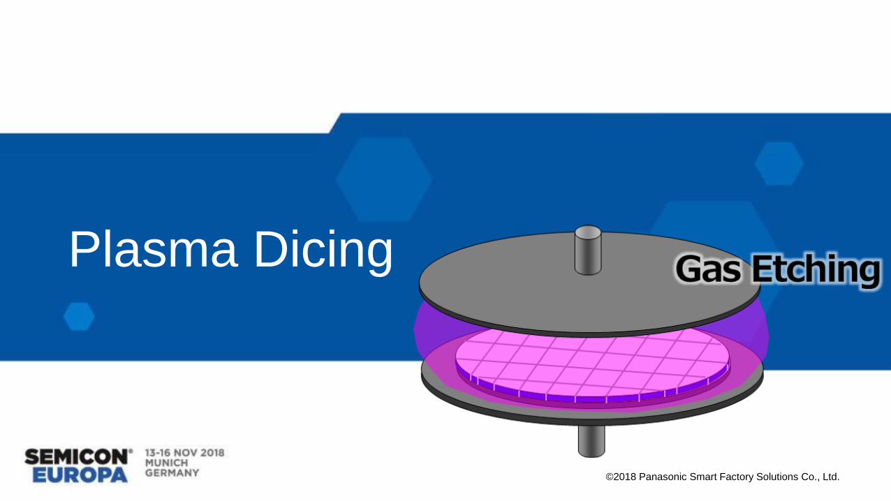
Plasma Dicing
©2018 Panasonic Smart Factory Solutions Co., Ltd.

IoT business growth and device evolution
MEMS sensors
Image sensors
= Integration
(sensor/
function integration)
= Miniaturization (CSPs)
Communication devices/
AP&BB/memory
= Higher frequency
= Integration (e.g. BB+RF)
= Thinner designs
CPU/GPU
memory
= Greater capacity,
faster
= Integration (3DIC, etc.)
Key devices
Sensing
High-speed processing
High-speed communication
Cloud
Business cycle with IoT applicationIoT business growth
IoT devices×100
millions
0
200
400
600
800
1,000
1,200
1,400
'15 '17 '19 '21 '23 '25 '27 '29
CAGR 12.1%’20⇒’30
5G
Phase1
5G
Phase2
Source: IHS Technology
High-speed communication
©2018 Panasonic Smart Factory Solutions Co., Ltd.

Demands for Dicing process
Trends of MEMS device.✓Low cost and High reliability✓High specification✓Down sizing (Light, Thin, small)✓Flexible design
Demands for Dicing process✓ Higher throughput✓ Damage free and stress free process✓ Higher accuracy dicing
©2018 Panasonic Smart Factory Solutions Co., Ltd.

Introduction of new process “Plasma dicing”
Blade dicing Plasma dicing
Gas Etching
✓ Damage Free✓ Need Mask Patterning
Mechanical
Chipping
✓ Damage✓ Low Machine Cost
©2018 Panasonic Smart Factory Solutions Co., Ltd.

Process flow with Laser and Plasma dicerPlasma Dicing Process
Mask patterning Dicing
Resist Coating Laser patterning Plasma dicing
Photo resist
Si
Mask
Metal/Low-k
TEG
Laser
Si
Mask
Si
Mask
Metal/Low-k
TEG
ACCRETECH Panasonic
APX300-DMAL300P
©2018 Panasonic Smart Factory Solutions Co., Ltd.

Process Flow
©2018 Panasonic Smart Factory Solutions Co., Ltd.

High reliable damage-less process
©2018 Panasonic Smart Factory Solutions Co., Ltd.

Blade dicing Plasma dicing
Optical
TEM
Damage & Chipping free
TEM
BG side
Chipping Nochipping
Damage(stress)
Nodamage
Device side
BG side
Device side
BG side
Chippingfree
BG side
Plasma dicing is no chipping and no damage process
©2018 Panasonic Smart Factory Solutions Co., Ltd.
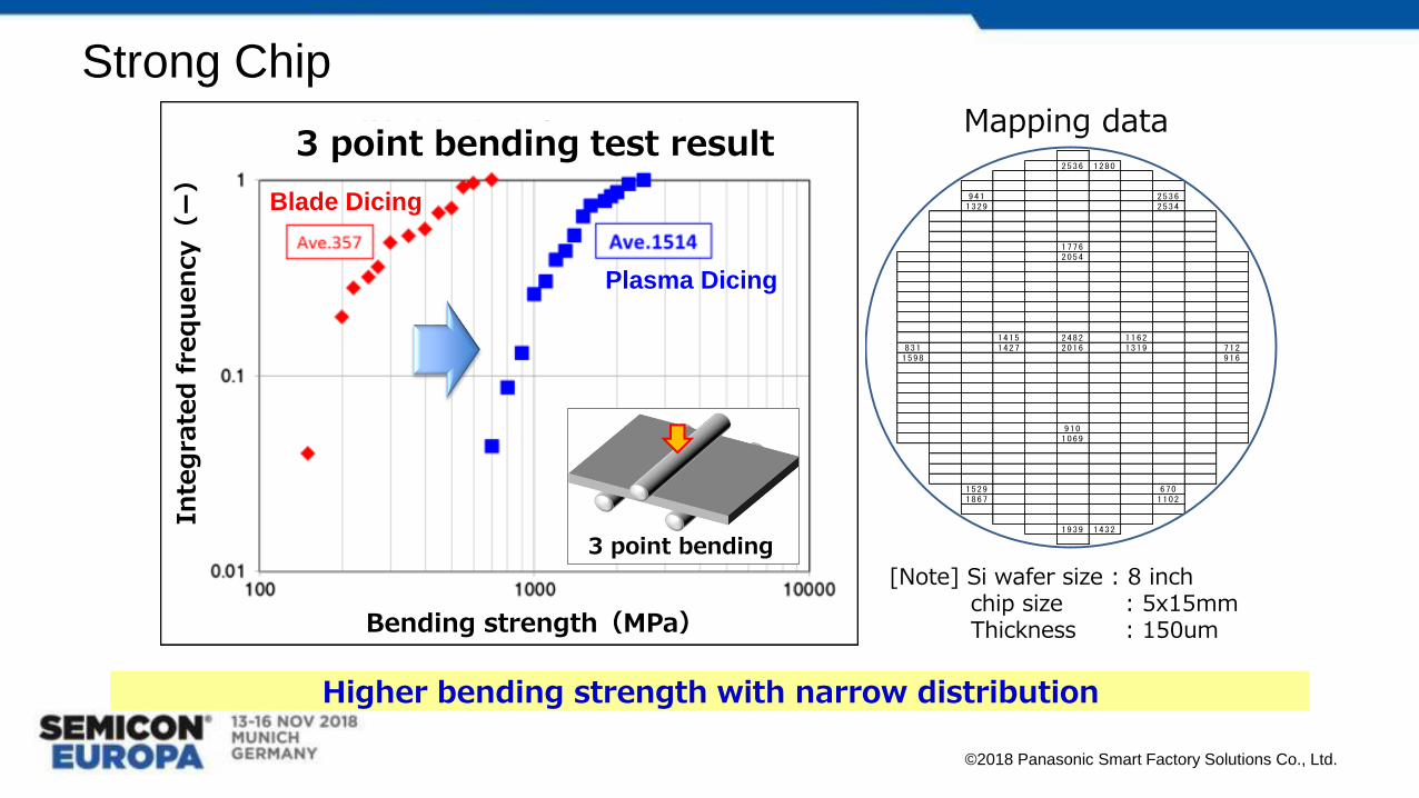
Strong Chip
2536 1280
941 25361329 2534
17762054
1415 2482 1162831 1427 2016 1319 7121598 916
9101069
1529 6701867 1102
1939 1432
Higher bending strength with narrow distribution
Mapping data
Plasma Dicing
Blade Dicing
[Note] Si wafer size : 8 inchchip size : 5x15mmThickness : 150um
3 point bending
Bending strength(MPa)
In
teg
rate
d f
req
uen
cy(
ー)
3 point bending test result
©2018 Panasonic Smart Factory Solutions Co., Ltd.

Comparison of breaking mode
Chipping due to dicing damage
Start breaking from chipping
No chipping
Original destruction mode of silicon
Blade dicing( Cleavage mode )
Plasma dicing( Crushing mode )
Brakingmode
Beforechip strength test
Afterchip strength test
Plasma dicing increases chip strength to original silicon strength
©2018 Panasonic Smart Factory Solutions Co., Ltd.

High accuracy dicing
©2018 Panasonic Smart Factory Solutions Co., Ltd.

High accuracy dicing
Blade dicing Plasma dicing
60μm
20μm
Wide chip marginMinimize chip margin
Device area
Device area
©2018 Panasonic Smart Factory Solutions Co., Ltd.

High yield process
©2018 Panasonic Smart Factory Solutions Co., Ltd.

More chips by street reduction
Blade dicing Plasma dicing
Num. of chips from one wafer
Blade Plasma
20µm
29,800
Street width
Num. of chips
60µm
27,500
+8% or more
(φ8inch, □1mm)
Morechips
60μm
20μm
Device area
Device area
©2018 Panasonic Smart Factory Solutions Co., Ltd.

Narrower dicing line
Die size: □1mm
©2018 Panasonic Smart Factory Solutions Co., Ltd.
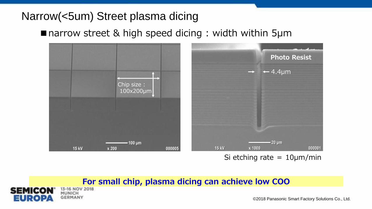
■narrow street & high speed dicing : width within 5μm
Silicon(50μm etching)
Narrow(<5um) Street plasma dicing
Si etching rate = 10μm/min
Chip size :100x200μm
4.4μm
Photo Resist
For small chip, plasma dicing can achieve low COO
©2018 Panasonic Smart Factory Solutions Co., Ltd.

Zigzag layout
©2018 Panasonic Smart Factory Solutions Co., Ltd.

Flexible design for MEMS
©2018 Panasonic Smart Factory Solutions Co., Ltd.
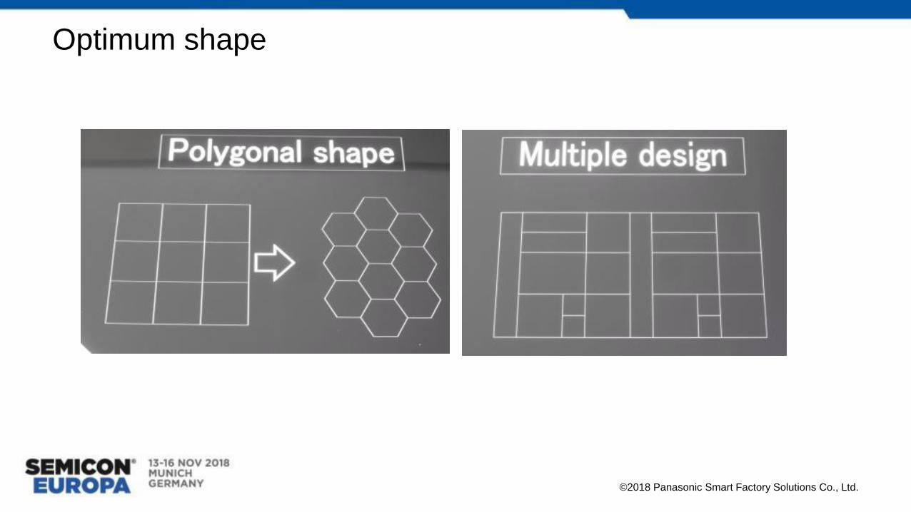
Optimum shape
©2018 Panasonic Smart Factory Solutions Co., Ltd.

SummaryPanasonic plasma can help high quality and low cost MEMS device production.
✓High reliabilityDamage-less and stress-free process
✓Optimum shapeFlexible mask design by laser patterning
✓High accuracy dicingChipping-free and Damage-free process
✓Maximum chip yieldMinimize dicing street and Zigzag layout
©2018 Panasonic Smart Factory Solutions Co., Ltd.

Plasma Dicing Demo Center in PSFS, Osaka, Japan
✓Total process can be test with entire plasma dicing method.
✓Collaborative researching on plasma dicing with our partner companies.
Material
Resist coater
System
Process
BG tape
BG
Plasma Dicer
Rinser
Measuring
DC tape
Plasma Dicing Demo Center
©2018 Panasonic Smart Factory Solutions Co., Ltd.

Conclusion

Conclusion
It will be required higher reliability process on the automotive market. Plasma dicing is able to meet this requirement.
Dicing method
and tools
Mechanical Internally focused LASER Plasma
Diamond Blade NIR pulse LASERLASER patterning and Plasma
etching
Surface protection Required protection film Not Required Required mask coating
Cleaning Required to remove protection film Not Required Required to remove mask
DamageRisk for mounting on and peeling off
the tapeNo damage No damage
Particle A large amount of particle Slight particle No particle
Die strength Low High Very high
Variant die
(Hexagon, etc.)Impossible Supported Supported
CoC Low LowLow
(Depend on wafer thickness and die size)
Reliability Low Middle High
Overall
There are a lot of risk on this
process. It will be able to apply
only for some specific MEMS.
It will be able to apply for most
of the MEMS devices. However
it is NOT perfect solution for
particle free.
It will be able to apply for most
of the MEMS. Moreover it is
perfect solution to avoid
contamination.

Thank you for your attention.