Embed Size (px)
Citation preview
IEEE JOURNAL OF QUANTUM ELECTRONICS, VOL. 56, NO. 1, FEBRUARY 2020 8400210
MEMS-Enabled Silicon Photonic IntegratedDevices and Circuits
Niels Quack , Senior Member, IEEE, Hamed Sattari , Alain Yuji Takabayashi, Yu Zhang, Peter Verheyen,
Wim Bogaerts , Senior Member, IEEE, Pierre Edinger , Carlos Errando-Herranz ,
and Kristinn B. Gylfason , Member, IEEE
(Invited Paper)
Abstract— Photonic integrated circuits have seen a dramaticincrease in complexity over the past decades. This developmenthas been spurred by recent applications in datacenter commu-nications and enabled by the availability of standardized maturetechnology platforms. Mechanical movement of wave-guidingstructures at the micro- and nanoscale provides unique oppor-tunities to further enhance functionality and to reduce powerconsumption in photonic integrated circuits. We here demon-strate integration of MEMS-enabled components in a simplifiedsilicon photonics process based on IMEC’s Standard iSiPP50GSilicon Photonics Platform and a custom release process.
Index Terms— Integrated optics, microelectromechanical sys-tems, nanophotonics, photonic integrated circuits, siliconphotonics.
I. INTRODUCTION
THE field of Silicon Photonics has been evolving rapidlyover the past decades [1], and today’s advanced standard-
ized technology platforms offered by specialized foundries,provide access to a broad catalog of high performancestandardized library components [2]–[5]. Passive componentsinclude low loss waveguides, crossings, grating and edge cou-plers, splitters and combiners, etc., while heaters, high-speedmodulators, and detectors, are representative of the active
Manuscript received June 21, 2019; revised September 17, 2019; acceptedOctober 7, 2019. Date of publication October 10, 2019; date of currentversion November 27, 2019. This work was supported by the EuropeanUnion’s Horizon 2020 Research and Innovation Programme (MORPHIC)under Agreement 780283. The work of N. Quack was supported by theSwiss National Science Foundation (SNSF) under Grant 157566. The workof H. Sattari was supported by the Hasler Foundation under Grant 17008.(Corresponding author: Niels Quack.)
N. Quack, H. Sattari, and A. Y. Takabayashi are with the École Polytech-nique Fédérale de Lausanne (EPFL), CH-1015 Lausanne, Switzerland (e-mail:[email protected]; [email protected]; [email protected]).
Y. Zhang is with Beihang University, Beijing 100083, China, and also withthe École Polytechnique Fédérale de Lausanne (EPFL), CH-1015 Lausanne,Switzerland (e-mail: [email protected]).
P. Verheyen is with the Interuniversity Microelectronics Centre (IMEC),3001 Leuven, Belgium (e-mail: [email protected]).
W. Bogaerts is with the Interuniversity Microelectronics Centre (IMEC),Department of Information Technology, 3001 Leuven, Belgium, and also withthe Center for Nano- and Biophotonics (NB Photonics), 9000 Ghent, Belgium(e-mail: [email protected]).
P. Edinger, C. Errando-Herranz, and K. B. Gylfason are with the Divisionof Micro and Nanosystems, School of Electrical Engineering and ComputerScience, KTH Royal Institute of Technology, SE-100 44 Stockholm, Sweden(e-mail: [email protected]; [email protected]; [email protected]).
Color versions of one or more of the figures in this article are availableonline at http://ieeexplore.ieee.org.
Digital Object Identifier 10.1109/JQE.2019.2946841
device selection. The tremendous advances in technologydevelopment allow to constantly augment the current technol-ogy platforms, and foundries continuously strive to integrateadditional technology modules to provide new functionalities.
Currently actively explored avenues for the enhancementof Photonic Integrated Circuit (PIC) technology seek toexploit high-performance materials [6], broaden the opticalwavelength range [7], integrate sources [8], enable biosens-ing [9], or to integrate quantum devices [10]. The integrationof such technology modules permits for example to overcomecurrent performance limits, to develop new applications, or toaddress entirely new concepts.
The combination of high performance photonic componentsat very large scale allows in particular to conceive fully recon-figurable photonic integrated circuits [11]–[13], providing apath for generic or ‘field-programmable’ PICs, where a singlephysical photonic network on-chip can be dynamically re-configured to address multiple functions [14].
This approach lowers the entry barrier for access to state-of-the art high performance PIC technology, and promisesat the same time a drastically reduced development timeand associate cost reductions. While implementations of suchprogrammable photonic integrated circuits have recently beendemonstrated experimentally [15], they remain at small scalewith up to a few tens of components only, limited by theinefficiency of the physical tuning mechanisms available incurrent PIC technology, such as the thermo-optic or the plasmadispersion effect.
Effectively, the scaling to very large photonic integratedcircuits imposes stringent requirements on the performanceof photonic components and requires suitable circuit archi-tectures and interfaces. In particular, any photonic devicefor large-scale integration has to provide (1) low opticalloss, (2) small footprint and (3) very low power consump-tion at the same time. In addition, (4) compatibility withexisting technology platforms is required to leverage thehigh performance achieved by the developments of the pastdecades.
Photonic devices augmented with micro-electromechanicalsystems (MEMS) exploit displacement or strain at the micro-and nanoscale, and provide a promising approach to addressthese challenges with compact, low-loss and low-powerconsumption actuation mechanisms. With Silicon Photonic
This work is licensed under a Creative Commons Attribution 4.0 License. For more information, see http://creativecommons.org/licenses/by/4.0/

8400210 IEEE JOURNAL OF QUANTUM ELECTRONICS, VOL. 56, NO. 1, FEBRUARY 2020
MEMS, strong optical effects can be achieved, and non-volatile states can be implemented by mechanical latching.In addition, MEMS represent a mature technology, and can bereadily integrated in existing technology platforms, reusing thefull library of existing high-performance photonic components.
II. MECHANICS FOR PHOTONICS
The integration of MEMS in PICs offers a range of physicalmechanisms to precisely control the optical signals on-chipand to provide added functionality. This section introducesthe salient aspects of mechanics for photonics, while a com-prehensive discussion of mechanical tuning in PICs and theoptical functions enabled thereby can be found in [16].
The underlying mechanics can be categorized into three cat-egories: displacement, strain, and buckling/stress (i.e., latch-ing). Displacement of a slab of material or a second waveguideinto the evanescent field of an active, light-carrying waveguidecan have one of two effects. If the slab material is notphase-matched to the active waveguide, it can induce lossesvia absorption, radiation, or scattering, or it can modify theeffective index of the waveguide. The former produces avariable optical attenuator (VOA) and the latter yields a phaseshifter, the effect for both of which is determined by thegap between slab material and waveguide. This gap is alsoimportant to the second case, where the movable body is asecond waveguide that can now support a guided mode of itsown. In this case, the gap, commonly referred to as a couplingdistance, can be varied to split various portions of the lightbetween the two waveguides. This type of device is a MEMS-tunable directional coupler and can be used as an optical powerdivider, or an optical switch when the power distribution in thebranches varies digitally.
Applying compressive or tensile stress to a waveguideintroduces a strain, which has been demonstrated to affectboth absorption and refraction [17]. When the strain primarilyaffects absorption, there is mechanical control over loss andthe result is once again a type of VOA. Similarly, modulatingthe refraction corresponds to changing the effective indexand the device acts as a phase shifter. The magnitude ofthe effect depends on the material properties and on thedevice orientation, as given by the elasto-optic matrix andthe mechanical and optical anisotropy. Furthermore, inducedstrain can also change waveguide length, which can be usedfor generating additional phase shifts.
The use of buckling/pre-stressed structures and latches isan approach enabled by MEMS that provides access to non-volatile states, and thus provides a path to ultra-low powerconsumption devices. In particular, after inducing the desiredoptical behavior using one of the above mechanisms, the phys-ical state of the system can be preserved without additionalconsumption of power. Buckling/pre-stressed beams have twomechanically stable states between which they can “snap”when displaced in a way that the induced stress exceeds ageometrically defined critical stress. Contact between comple-mentary hooks on functional and latching structures constitutesanother method for maintaining stable states. The hooks onthe latch are released to allow the functional body to moveand then are locked to prevent a return to the initial position.
Fig. 1. (a) In-plane and (b) out-of-plane electrostatic devices.
In both cases, the only energy expenditure is in transitioningbetween states; thus, the possibility of zero-passive powermechanical latching is an additional benefit of using MEMSto realize optical functions.
III. SILICON PHOTONIC MEMS
The mechanics for photonics discussed in the previoussection all rely on actuation mechanisms to generate forces thatare translated either to a displacement or to stress. In SiliconPhotonics, electrostatic actuation is commonly used, due toits ease of integration, low power consumption, fast responsetimes, large displacements and fine displacement resolution.A variety of additional actuation mechanisms for PhotonicMEMS are possible and are discussed in more detail in [16].
Electrostatic actuation relies on the attractive force betweenthe movable and fixed plates of a charged capacitor and therestoring spring force of a suspension. By varying the voltage,the movable plate undergoes displacement, the direction ofwhich depends on the mechanical degree of freedom and thecapacitor geometry. Typically, parallel-plate arrangements areemployed for out-of-plane movement and the interdigitatedfinger structure of comb-drives are used for in-plane move-ment. These devices can be fabricated both in single andstacked photonic layer arrangements.
A. Single Photonic Layer MEMS
In the single photonic layer approach, the actuators arepatterned in the device layer of a silicon-on-insulator (SOI)wafer and released in a post-fabrication step through removalof the sacrificial, buried oxide (BOX) layer. Both in-plane [18]and out-of-plane [19] arrangements are possible as shown inFig. 1.
B. Stacked Photonic Layer MEMS
Stacked photonic layers provide an attractive alternativeapproach with additional degrees of freedom: a second pho-tonic MEMS layer is deposited atop a sacrificial material,and its vertical spacing to the first layer is defined by a setof mechanical stoppers. However, this approach requires cus-tomized process steps which are not part of today’s standardsilicon photonic platforms, which can provide challenges intemperature budget and processing compatibility with highperformance photonic devices. Still, dedicated processes haveyielded the largest scale integrated photonic switches to date[20], [21] and digital phase shifters [22]. Further, designs forVOAs [23], analog phase shifters [24], and latched devices[25] have been proposed. A schematic cross-section showinga standard parallel-plate capacitor arrangement, and one usingvertical comb-drives and bistable beams is given in Fig. 2.

QUACK et al.: MEMS-ENABLED SILICON PHOTONIC INTEGRATED DEVICES AND CIRCUITS 8400210
Fig. 2. Multilayer electrostatic devices (a) parallel-plate driven (b) verticalcomb-drive driven with bistability.
IV. INTEGRATED DEVICES
In order to integrate Silicon Photonic MEMS devices inexisting Silicon Photonics platforms, mechanical degrees offreedom have to be provided. Typically, this requires theselective removal of the cladding oxide around the siliconwaveguides in certain areas on the photonic integrated cir-cuit, which enables both movable structures as electrostaticactuation as described in section section III.A. Such a selec-tive removal can be achieved by a dedicated post-processingsequence using standard microfabrication techniques on fullyprocessed Silicon Photonics substrates.
In addition, the introduction of MEMS capability to siliconphotonics requires the design and development of a basicset of dedicated components. Among the enabling functionsfor a MEMS-enhanced silicon photonics platform are low-loss optical transitions between oxide-clad and air-clad siliconwaveguides, resonators, couplers and phase-shifters.
This section describes in detail the manufacturing processfor MEMS-enabled integrated devices in Silicon Photon-ics, and introduces design and experimental results for aset of selected basic, fully released components. While theresults demonstrate the capability of the MEMS integrationapproach and the performance of selected MEMS components,the impact of this powerful technique extends far beyondthe demonstrated devices, as it will enable photonic circuitdesigners with a powerful toolbox to conceive an entirely newclass of integrated silicon photonic MEMS devices.
A. Fabrication Process
Devices were designed and fabricated in a simplified versionof IMEC’s iSiPP50G standard silicon photonics technologyplatform [2], [26], where several process modules (such as formodulators, detectors and metal routing) have been omitted tospeed up process development while maintaining full passivesfunctionality as well as topology and surface finish which arerepresentative for the full process. The release process wasdeveloped and performed at the Center of MicroNanoTech-nology (CMi) at EPFL [27]. A graphic representation of therelease process is shown in Fig. 3.
The fully processed 200 mm silicon photonics wafers arefirst diced into 12 coupons, each of which consists of fourdies (22 mm × 24 mm). The coupon size is chosen forease of handling and minimizing process development risks.Although process development and MEMS release wereperformed on coupon- and chip-level, all process steps arewafer-level compatible, allowing direct transfer to a foundryand also to include wafer level packaging for hermetic sealingat a later stage.
After a thorough removal of the photoresist (PR) layer usedas a protective layer for transport, coupons are subjected toatomic layer deposition (ALD, Beneq TFS200) of 50 nmAlumina (Al2O3) at 200 ◦C, during roughly 40 minutes.Alumina serves as an excellent hardmask against vapor HFand its refractive index of 1.75 in the C-band is sufficientlyclosely matched to that of silicon dioxide, precluding theneed to remove it above grating couplers used for optical I/O.The alumina thickness is selected by considering the tradeoffbetween the minimum thickness needed to provide sufficientcoverage across the wafer topology and the maximum tolerablethickness for reducing its influence on optical behavior. Depo-sition by ALD produces layers that are uniform, conformal,and pin-hole free, providing excellent protection against HFvapor attack of any underlying oxide layers.
The patterning of the alumina to open up regions withinthe MEMS cavities begins with an exposure of the 6 μmthick photoresist (AZ ECI 3027) using direct laser-writing(Heidelberg Maskless Aligner MLA150). A thick photoresistis used to provide adequate coverage of the topology and useof the maskless aligner allows for adjustment of the aluminaopenings in a layout editing software without the need tocreate a new physical photomask. The alignment accuracy ofthe exposure is within ± 600 nm, which is adequate for thepositioning of the release windows. Next, the alumina is etchedin an inductively coupled plasma etcher where a 10% overetchis added to ensure that the alumina is fully removed in regionswhere the oxide should be exposed to the vapor HF.
Post-etch PR removal starts with a 2-minute low-power oxy-gen plasma strip to remove the topmost layer and is followedby a full 15-minute immersion in a heated liquid remover(Remover 1165 at 70 ◦C). The final step is an additionaloxygen plasma strip to ensure no PR-based residues remain.Dicing of the coupons into individual chips is performed usingan automatic dicing saw (Disco DAD321).
Vapor phase HF (SPTS uEtch) is chosen for the removalof the oxide to reduce the risk of stiction and because liquidphase HF can attack aluminum, which is typically used inmetallization layers for bondpads. The release process takesupwards of 4 hours and is performed at a low chamber pressure(80 Torr) in a sequence of 12 cycles, each of which includesa stabilization period, an etch sequence, and a purge/pumpstep to remove the water byproduct of the etch. The processis repeatable and designed to be fully compatible with theiSiPP50G platform. The vapor phase HF does not attack thebond pads and the alumina passivation sufficiently protects theMEMS cavity sidewalls lining the back-end-of-line (BEOL)stack.
B. Experimental Characterization
A schematic representation of the characterization setupis depicted in Fig. 4(a). It includes a tunable laser (Agilent8164A) with tuning range from 1460 nm to 1580 nm, a detec-tor module, a polarization controller, a fiber array with 127 μmfiber pitch, and a pair of electrical probe tips. The polarizedlight from the tunable laser is guided by a single mode fiber,and it couples vertically to the photonic circuit. An efficient

8400210 IEEE JOURNAL OF QUANTUM ELECTRONICS, VOL. 56, NO. 1, FEBRUARY 2020
Fig. 3. Silicon Photonic MEMS release process: (a) 200 mm Silicon Photon-ics Wafer, diced into 44 mm × 48 mm coupons with initial cross section (b),followed by (c) alumina atomic layer deposition, (d) photolithography andalumina opening by inductively coupled plasma etching. (e) Separation ofcoupons into 22 mm × 24 mm dies before (f) selective etching of the buriedoxide layer by vapor HF etching to achieve stiction free MEMS release.
Fig. 4. (a) Schematic of the characterization setup. (b) Arrangement of thefiber array, the photonic chip, and the electrical probe tips.
fiber to chip light coupling is enabled by an integrated gratingcoupler on the chip. After on-chip propagation, the light isout-coupled from the chip to another fiber in the fiber arrayby means of one of the integrated grating couplers. The out-coupled light is guided by the fiber to the detector where wecan extract the transmission spectrum of the integrated deviceunder test. The picture in Fig. 4(b) shows the arrangementof the fiber array, photonic chip and the electrical probe tips.A precise alignment between the fiber array and the integratedgrating couplers is essential to have an efficient light couplingbetween the fibers and the grating couplers. This is accessibleby precise tuning of the fiber array position over the chip usinga positioning stage with six degrees of freedom. Furthermore,we mount the chip on a stage with three degrees of freedomin positioning which facilitates precise fiber array alignmentto the chip. We measure a ∼3.1 dB coupling loss per gratingcoupler at 1530 nm, which is obtained by measuring lighttransmission from one grating coupler to the other one with noother integrated device interacting with the propagating light.We use a grating-to-grating transmission spectrum in each setof measurements for normalization of the transmission spectraof the test devices to discard loss introduced by the couplers.
Fig. 5. (a) Optical image of a series of 22 optical transitions integrated withtwo grating couplers, (b) a close-up of the transitions. The color change onthe tapered part shows the etched oxide front due to the HF vapor release step,and (c) the simulated normalized electric field profile in the optical transitionat λ = 1550 nm.
C. Low-Loss Optical Transitions for MEMS Devices
Inside the MEMS cavities the components are exposed toair, while on the remaining areas of the PIC, the photonicdevices are fully oxide-clad. When entering the MEMS cavity,the guided light experiences a transition from the air-clad zoneto the oxide-clad zone, and consequently a residual amountof light is reflected back due to a mismatch of mode indexbetween the two environments. In addition, for most of thefreestanding components in this platform the optical transitionsact also as mechanical anchors. Therefore, a careful design ofthe optical transition in the border of the MEMS cavities isrequired to first minimize scattering loss and reflection back tothe circuit, and secondly, to prevent HF vapor from penetratinginto the materials of the BEOL stack atop the oxide cladding.
We implement various types of optical transitions in theplatform using: deep-to-shallow tapered waveguide structures,multimode interference (MMI)-based structures, and photoniccrystal-based structures. Our inspections show that the deep-to-shallow tapered structures have an excellent performancefrom the standpoint of loss values and blocking HF vaporaccess to the BEOL. In this kind of transition the guidedmode in the freestanding fully etched (wire or ridge) 214 nmhigh and 450 nm wide waveguide smoothly transfers to aguided mode in a 70 nm shallow etched rib waveguide withthe same width. The mode transition happens along a 15 μmlong waveguide tapering.
In order to experimentally estimate the loss of an individualoptical transition we measure the transmission of a waveguidewhich passes through several (22, 30, 42) transitions, andextrapolate the loss for a single transition from a linear datafit. An optical microscope recording of a series of 22 air-to-oxide transitions is shown in Fig. 5(a). A closer view of thecomponent in Fig. 5(b) shows the HF vapor etch-front which isstopped by the shallow waveguide at the border of the MEMS

QUACK et al.: MEMS-ENABLED SILICON PHOTONIC INTEGRATED DEVICES AND CIRCUITS 8400210
Fig. 6. (a) The measured transmission spectra for three series of opticaltransitions and (b) the simulated transmission and reflection spectra for asingle optical transition. The layout of the optical transition is presented inthe inset.
cavity. In Fig. 5(c) we present the normalized electric fielddistribution at λ = 1550 nm while the light passes from the aircladding to the oxide cladding through the optical transition,which is extracted from a 3D finite difference time domain(FDTD) simulation.
The measurements for all three sets of transitions are shownin Fig. 6(a) and performing a linear fit on the case of 22 and30 transitions yields a loss of approximately 0.07 dB pertransition at λ = 1550 nm. The case for 42 transitions isomitted from the regression because the large ripples are bothuncharacteristic and unexpected. We attribute this ripple inthe spectra to backreflections from the MEMS cavity borders,which build up along the waveguide sections inside the cavity.This effect is expected to be minimized by further designoptimization. Our 3D FDTD simulations predict a very lowreturn loss of ∼ 37 dB per transition at λ = 1550 nm dueto the waveguide cladding mismatch for this type of opticaltransition. The simulation results for a single optical transitionis presented in Fig. 6(b).
D. Suspended Directional Coupler
Directional couplers are an essential building block of anyintegrated photonic circuit for photonic routing and powerdistribution between components. For integration with MEMSin PICs, specific implementation of a freestanding directionalcoupler is thus required. For such a directional coupler a minia-turized footprint and a low loss performance are paramount toreduce risk of stress-related and release process failures andto keep the overall area of the circuit small in order to scaleto circuits with numerous directional couplers.
We here present an implementation of a compact widebanddirectional coupler for MEMS-enabled integrated components[28]. A representative schematic (not to scale) of the compo-nent with the related dimensions is presented in Fig. 7(a).
The coupling region includes two symmetric arms eachincluding two tapered and one narrow straight waveguides.
Fig. 7. (a) The schematic of the suspended directional coupler (not to scale).The optical mode profile is shown for two cross-sections: at the input and inthe middle of the coupler. (b) SEM image of the released directional coupler.
Fig. 8. Measured and simulated power spectra, normalized to the gratingcouplers and straight waveguides, at the drop and through ports of thefreestanding directional coupler.
The tapered waveguides are tapered from 450 nm to 300 nmin width along 10 μm, and are connected to a 300 nm wideand 1 μm long straight section in the middle. The couplingregion is supported by a set of 5 μm radius bent waveguides.This leads to a compact footprint of ∼ 30×20 μm2 by takinginto account the waveguide anchors (transitions).
Performance of the component is simulated using theFDTD method which gives the transmission spectrum of thecomponent and also the optical mode profile in any desiredcross-section. The scanning electron microscope (SEM) imageof the realized component is depicted in Fig. 7(b) whichexhibits the MEMS release window and the optical air-to-oxide cladding transitions waveguides and anchors. The SEMrecording reveals a cleanly released component with couplerarms well-positioned with respect to each other (parallel).
The measured and simulated power spectra at the throughand drop ports of the coupler are presented in Fig. 8.

8400210 IEEE JOURNAL OF QUANTUM ELECTRONICS, VOL. 56, NO. 1, FEBRUARY 2020
Fig. 9. The dimensions of the freestanding silicon photonic (a) disk and (b)ring resonators.
Fig. 10. SEM micrographs of (a) the disk and (b) the ring resonatorswith freestanding coupling waveguides, oxide cladding openings and releasewindows.
The component is designed to operate in telecommunicationC-band (1530 nm – 1565 nm). Although the port extinctionratio (ER) measured across the full C-band is less than 10 dB,there is a good ER of 25 dB at the targeted 1550 nmwavelength, with a more modest 20 dB ER within a 10 nmbandwidth around this central wavelength. The lowest inser-tion loss of 0.5 dB is measured at 1560 nm. Note thatthere is a 5 nm discrepancy between the simulated and themeasured spectra which we attribute to possible fabricationbias or residual misalignment between the waveguides.
E. Freestanding Disk and Ring Resonators
Disk and ring resonators serve as spectral filters andswitches in photonic integrated circuits [29]. Applying theselective MEMS release process introduced in section IV.Aallows to provide mechanical degrees of freedom, and fullyintegrated optomechanical oscillators [30] can be obtained inthis way [31]. In combination with movable waveguides, diskand ring resonators can be explored for MEMS tunable filterswith add/drop capabilities. We implemented disk and ringresonators with dimensions as shown in Fig. 9.
The radius of the disk is 10 μm, and the air gap betweendisk and coupling waveguide is 140 nm. For the ring resonator,the outside and inside radii are 20 μm and 14 μm, respec-tively, and the air gap is 130 nm. The thickness of couplingwaveguides is 214 nm, the 450 nm wide waveguide extends48 μm with a low loss transition on each side, and with thedisk/ring of corresponding radius located at the center. SEMrecordings of the coupling waveguide with the disk and ringresonators are shown in Fig. 10.
The disk and ring resonators are anchored to the substrate bycentral silicon oxide pillars, which have not been fully etched,and the freestanding coupling waveguides are suspended atboth sides.
Fig. 11. Measured transmission spectra of (a) the disk resonator and (b) thering resonator with optical Q-factor more than 3.6 × 10⁴ and extinction ratiolarger than 20 dB.
In the same figure, the oxide cladding opening and releasewindow can clearly be distinguished. Optical characterizationis performed by means of the experimental setup describedin Section IV-B. The experimentally recorded transmissionspectrum of the disk and ring resonators are represented inFig. 11.
The optical Q-factors are obtained by fitting a Lorentzianfunction to the resonances. Both for the freestanding diskresonator and the ring resonator, we confirm a high loadedoptical Q-factor up to 3.6×10⁴ with an extinction ratio largerthan 20 dB.
F. Photonic MEMS Actuation
Applying the release process introduced in section IV.Ato waveguides with MEMS actuation structures allows forMEMS-actuated photonic devices. As introduced in III.A.,when using the single-layer approach the displacement caneither be in-plane (comb-drive actuators), or out-of-plane(parallel-plate actuation).
In order to validate the platform for actuation, phase shifterswere designed and experimentally tested. We have validatedsuch devices on simple SOI wafers with identical device layer/ buried oxide layer dimensions previously [32], and slightlydifferent SOI stacks have been reported by other groups aswell [33]. Compared to previously reported prototypes basedon e-beam lithography, the here reported devices additionallybenefit from doping and low-resistance contacts and willenable time responses limited by the mechanics only.
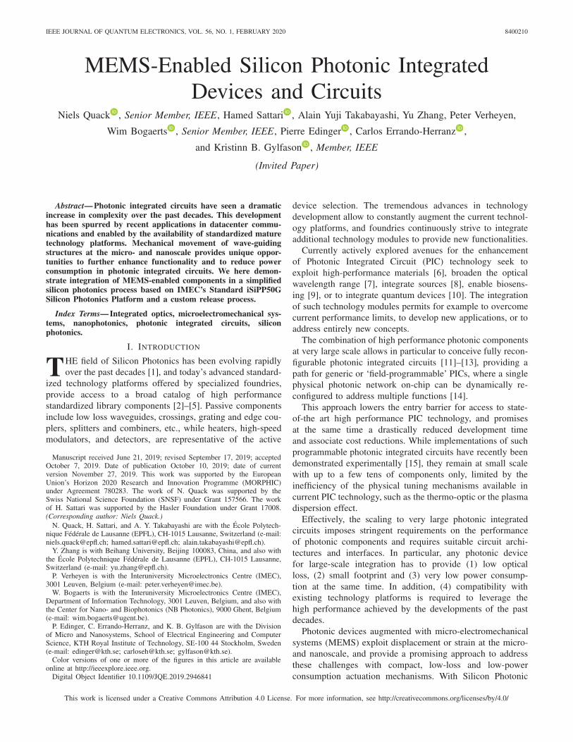
Two representative examples of phase shifters are shownin Fig. 12, using out-of-plane (a) and in-plane (b) actua-tion respectively. The out-of-plane version relies on parallel-plate actuation of a suspended membrane to move a narrowbeam downwards away from the waveguiding beam, whichdecreases the effective index. The in-plane version utilizescomb-drive actuators to increase the gap between suspendedwaveguide and narrow beam horizontally, similarly reducingthe effective index. Both types of phase shifters were insertedin unbalanced Mach-Zehnder Interferometers (MZI) with lowFree Spectral Range (FSR), in order to experimentally extract
QUACK et al.: MEMS-ENABLED SILICON PHOTONIC INTEGRATED DEVICES AND CIRCUITS 8400210
Fig. 12. (a) Effective index tuning with in-plane or out-of-plane displacementof a narrow Si beam. (b) Phase shifter relying on out-of-plane displacementof a narrow Si beam, and (c) Similar tuning but with in-plane displacement,thanks to a comb-drive actuator.
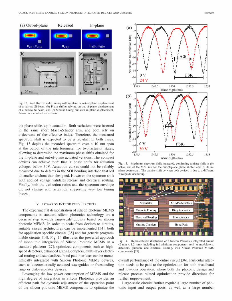
the phase shifts upon actuation. Both variations were insertedin the same short Mach-Zehnder arm, and both rely ona decrease of the effective index. Therefore, the measuredspectrum shift is expected to be a red-shift in both cases.Fig. 13 depicts the recorded spectrum over a 10 nm spanat the output of the interferometer for two actuator states,allowing to determine the maximum phase shifts obtained forthe in-plane and out-of-plane actuated versions. The compactdevices can achieve more than π phase shifts for actuationvoltages below 30V. Actuation curves could not be reliablymeasured due to defects in the SOI bonding interface that ledto smaller anchors than designed. However, the spectrum shiftwith applied voltage validates release and electrical routing.Finally, both the extinction ratios and the spectrum envelopedid not change with actuation, suggesting very low tuninglosses.
V. TOWARDS INTEGRATED CIRCUITS
The experimental demonstration of silicon photonic MEMScomponents in standard silicon photonics technology are adecisive step towards large-scale circuits based on siliconphotonic MEMS. In order to scale from devices to circuits,suitable circuit architectures can be implemented [34], bothfor application specific circuits [35] and for generic program-mable circuits [14]. Fig. 14 illustrates the powerful approachof monolithic integration of Silicon Photonic MEMS in astandard platform [27]: optimized components such as high-speed detectors, enhanced grating-couplers, multi-layer electri-cal routing and standardized bond pad interfaces can be mono-lithically integrated with Silicon Photonic MEMS devices,such as electrostatically actuated waveguides or freestandingring- or disk-resonator devices.
Leveraging the low power consumption of MEMS and thehigh degree of integration in Silicon Photonics provides anefficient path for dynamic adjustment of the operation pointof the silicon photonic MEMS components to optimize the
Fig. 13. Maximum spectrum shift measured, confirming a phase shift in theactive arm of the MZI. (a) For the out-of-plane phase shifter, and (b) its in-plane counterpart. The passive shift between both devices is due to a differentwaveguide anchoring.
Fig. 14. Representative illustration of a Silicon Photonics integrated circuit(2 mm × 1.2 mm), including full platform components such as modulators,detectors, photonic and electrical routing, with Silicon Photonic MEMScomponents [27].
overall performance of the entire circuit [36]. Particular atten-tion needs to be paid to the optimization for both broadbandand low-loss operation, where both the photonic design andrelease process related optimization provide directions forfurther improvement.
Large-scale circuits further require a large number of pho-tonic input and output ports, as well as a large number

8400210 IEEE JOURNAL OF QUANTUM ELECTRONICS, VOL. 56, NO. 1, FEBRUARY 2020
of electrical interfaces for both low-frequency (<10 MHz)for MEMS actuation, as well as for high-speed (>50 GHz)modulators and photodetectors. Current integration efforts areaddressing these challenges [37]. The voltage levels requiredin demonstrated Silicon Photonic MEMS devices are typicallyseveral 10s of volts. While discrete electronic amplifier arrayscan reach such relatively high voltages, lowering the requiredactuation voltages can provide benefits in terms of integrationwith integrated electronic circuits. Avenues to reach loweractuation voltages can be explored with adequate MEMSdesign, such as by decreasing the spring constant of thewaveguide suspension. However, a tradeoff in actuation speedhas to be taken into consideration in view of the resulting lowermechanical resonance frequencies. Finally, in order to ensurelong-term stability of the MEMS devices [38], sealing of theMEMS cavities is required, for which wafer-level packagingtechniques for MEMS [39] can be employed.
VI. CONCLUSION
We have demonstrated the integration of MEMS-enableddevices based on a simplified silicon photonics platform witha custom post-processing module. Experimental results onoptical performance for selected representative Silicon Pho-tonic MEMS components including freestanding broadbanddirectional couplers, MEMS-actuated phase shifters, oxide-clad to air-clad waveguide transitions and ring/disk resonatorsare reported.
We demonstrate a MEMS release process that is entirelycompatible with IMEC’s standard ISIPP50G platform. In par-ticular, no high-temperature processing is required and therelease step preserves the integrity of the metal contact padsby virtue of the anhydrous HF etching process.
In summary, Silicon Photonic MEMS provide an outstand-ing potential for low-power and high-performance photonicdevices and lay the ground for efficient integration in verylarge-scale photonic integrated circuits such as required inprogrammable and reconfigurable photonic integrated circuits.
ACKNOWLEDGMENT
The MEMS release process was performed at the Centerfor Micro- and Nanotechnology (CMi) at EPFL. The authorswish to acknowledge the support by the CMi technical staffin the development of the release process.
REFERENCES
[1] R. Soref, “The past, present, and future of silicon photonics,” IEEEJ. Sel. Topics Quantum Electron., vol. 12, no. 6, pp. 1678–1687,Nov. 2006.
[2] M. Pantouvaki et al., “50Gb/s Silicon Photonics Platform for Short-Reach Optical Interconnects,” in Opt. Fiber Commun. Conf. (OSA)Tech. Dig. Washington, DC, USA: OSA, 2016, Paper Th4H.4. [Online].Available: https://www.osapublishing.org/abstract.cfm?uri=OFC-2016-Th4H.4
[3] K. Giewont et al., “300-mm monolithic silicon photonics foundrytechnology,” IEEE J. Sel. Topics Quantum Electron., vol. 25, no. 5,Sep./Oct. 2019, Art. no. 8200611.
[4] E. Timurdogan et al., “AIM process design kit (AIMPDKv2.0): Siliconphotonics passive and active component libraries on a 300mm wafer,”in Proc. Opt. Fiber Commun. Conf. Expo., Mar. 2018, pp. 1–3.
[5] A. E.-J. Lim et al., “Review of silicon photonics foundry efforts,”IEEE J. Sel. Topics Quantum Electron., vol. 20, no. 4, Jul./Aug. 2014,Art. no. 8300112.
[6] B. Desiatov, A. Shams-Ansari, M. Zhang, C. Wang, and M. Loncar,“Ultra-low-loss integrated visible photonics using thin-film lithium nio-bate,” Optica, vol. 6, no. 3, pp. 380–384, Mar. 2019.
[7] P. Muñoz et al., “Silicon nitride photonic integration platforms forvisible, near-infrared and mid-infrared applications,” Sensors, vol. 17,no. 9, p. 2088, Sep. 2017.
[8] J. Zhang et al., “Transfer-printing-based integration of a III-V-on-silicondistributed feedback laser,” Opt. Exp., vol. 26, no. 7, pp. 8821–8830,Apr. 2018.
[9] K. De Vos, I. Bartolozzi, E. Schacht, P. Bienstman, and R. Baets,“Silicon-on-insulator microring resonator for sensitive and label-freebiosensing,” Opt. Exp., vol. 15, no. 12, pp. 7610–7615, Jun. 2007.
[10] J. W. Silverstone, D. Bonneau, J. L. O’Brien, and M. G. Thompson,“Silicon quantum photonics,” IEEE J. Sel. Topics Quantum Electron.,vol. 22, no. 6, pp. 390–402, Nov./Dec. 2016.
[11] J. Carolan et al., “Universal linear optics,” Science, vol. 349,pp. 711–716, Aug. 2015.
[12] J. Capmany, I. Gasulla, and D. Pérez, “Microwave photonics: Theprogrammable processor,” Nature Photon., vol. 10, no. 1, pp. 6–8,Jan. 2016.
[13] D. Pérez, I. Gasulla, J. Capmany, and R. A. Soref, “Reconfigurablelattice mesh designs for programmable photonic processors,” Opt. Exp.,vol. 24, no. 11, pp. 12093–12106, May 2016.
[14] D. Pérez et al., “Multipurpose silicon photonics signal processor core,”Nature Commun., vol. 8, no. 1, p. 636, Sep. 2017.
[15] A. Ribeiro, A. Ruocco, L. Vanacker, and W. Bogaerts, “Demonstra-tion of a 4×4-port universal linear circuit,” Optica, vol. 3, no. 12,pp. 1348–1357, Dec. 2016.
[16] C. Errando-Herranz, A. Y. Takabayashi, P. Edinger, H. Sattari,K. B. Gylfason, and N. Quack, “MEMS for photonic integratedcircuits,” IEEE J. Sel. Topics Quantum Electron., to be published.[Online]. Available: https://ieeexplore.ieee.org/document/8847362. doi:10.1109/JSTQE.2019.2943384.
[17] Y. Kim, M. Takenaka, T. Osada, M. Hata, and S. Takagi, “Strain-inducedenhancement of plasma dispersion effect and free-carrier absorption inSiGe optical modulators,” Sci. Rep., vol. 4, p. 4683, Apr. 2014.
[18] S. Han, T. J. Seok, C.-K. Kim, R. S. Müller, and M. C. Wu, “Mul-ticast silicon photonic MEMS switches with gap-adjustable directionalcouplers,” Opt. Exp., vol. 27, no. 13, pp. 17561–17570, Jun. 2019.
[19] S. Han, T. J. Seok, N. Quack, B.-W. Yoo, and M. C. Wu, “Large-scalesilicon photonic switches with movable directional couplers,” Optica,vol. 2, no. 4, pp. 370–375, 2015.
[20] T. J. Seok, N. Quack, S. Han, R. S. Müller, and M. C. Wu, “Large-scale broadband digital silicon photonic switches with vertical adiabaticcouplers,” Optica, vol. 3, no. 1, pp. 64–70, Jan. 2016.
[21] T. J. Seok, K. Kwon, J. Henriksson, J. Luo, and M. C. Wu, “Wafer-scalesilicon photonic switches beyond die size limit,” Optica, vol. 6, no. 4,pp. 490–494, Apr. 2019.
[22] J. Henriksson, T. J. Seok, J. Luo, K. Kwon, N. Quack, and M. C. Wu,“Digital silicon photonic MEMS phase-shifter,” in Proc. Int. Conf. Opt.MEMS Nanophoton., Lausanne, Switzerland, Jul./Aug. 2018, pp. 1–2.
[23] T. Graziosi, H. Sattari, T. J. Seok, S. Han, M. C. Wu, and N. Quack,“Silicon photonic MEMS variable optical attenuator,” Proc. SPIE,MOEMS and Miniaturized Systems XVII, vol. 10545, Feb. 2018,Art. no. 105450H. [Online]. Available: https://www.spiedigitallibrary.org/conference-proceedings-of-spie/10545/105450H/Silicon-photonic-MEMS-variable-optical-attenuator/10.1117/12.2317507.short
[24] H. Sattari et al., “Silicon photonic MEMS phase-shifter,” Opt. Exp.,vol. 27, no. 13, pp. 18959–18969, Jun. 2019.
[25] H. Sattari, A. Toros, T. Graziosi, and N. Quack, “Bistable siliconphotonic MEMS switches,” Proc. SPIE, MOEMS and MiniaturizedSystems XVIII, vol. 10931, Mar. 2019, Art. no. 109310D. [Online].Available: https://www.spiedigitallibrary.org/conference-proceedings-of-spie/10931/2507192/Bistable-silicon-photonic-MEMS-switches/10.1117/12.2507192.full
[26] P. P. Absil et al., “Imec iSiPP25G silicon photonics: A robust CMOS-based photonics technology platform,” Proc. SPIE, vol. 9367, Feb. 2015,Art. no. 93670V.
[27] J. Jacobs et al., “Die level release of silicon photonic MEMS,” in Proc.Int. Conf. Opt. MEMS Nanophoton., Jul./Aug. 2016, pp. 1–2.
[28] H. Sattari, Y. Zhang, A. Y. Takabayashi, and N. Quack, “Silicon photonicbroadband suspended directional coupler,” in Proc. Int. Conf. Opt.MEMS Nanophoton. Daejeon, South Korea: KAIST, Jul./Aug. 2019,pp. 214–215.
[29] W. Bogaerts et al., “Silicon microring resonators,” Laser Photon. Rev.,vol. 6, no. 1, pp. 47–73, Jan. 2012.

QUACK et al.: MEMS-ENABLED SILICON PHOTONIC INTEGRATED DEVICES AND CIRCUITS 8400210
[30] M. Aspelmeyer, T. J. Kippenberg, and F. Marquardt, “Cavity optome-chanics,” Rev. Mod. Phys., vol. 86, no. 4, pp. 1391–1452, Dec. 2014.
[31] Y. Zhang, A. Y. Takabayashi, H. Sattari, and N. Quack, “Freestandingsilicon photonic ring and disk resonators,” in Proc. Int. Conf. Opt. MEMSNanophoton. Daejeon, South Korea: KAIST, Jul./Aug. 2019, pp. 212–213.
[32] P. Edinger, C. Errando-Herranz, and K. Gylfason, “Low-loss MEMSphase shifter for large scale reconfigurable silicon photonics,” presentedat the 32nd IEEE Int. Conf. Micro Electro Mech. Syst., 2019.
[33] T. Ikeda, K. Takahashi, Y. Kanamori, and K. Hane, “Phase-shifterusing submicron silicon waveguide couplers with ultra-small electro-mechanical actuator,” Opt. Exp., vol. 18, no. 7, pp. 7031–7037,Mar. 2010.
[34] D. P. López and J. Capmany, “Programmable multifunctionalnanophotonic ICs: Architectures, performance, and challenges,”Proc. SPIE, Smart Photonic and Optoelectronic IntegratedCircuits XXI, vol. 10922, Mar. 2019, Art. no. 1092213. [Online].Available: https://www.spiedigitallibrary.org/conference-proceedings-of-spie/10922/1092213/Programmable-multifunctional-nanophotonic-ICs-architectures-performance-and-challenges/10.1117/12.2511257.full
[35] D. Celo et al., “32×32 silicon photonic switch,” in Proc. 21st OptoElec-tron. Commun. Conf. (OECC) Held Jointly Int. Conf. Photon. Switching,Jul. 2016, pp. 1–3.
[36] I. Zand, B. Abasahl, U. Khan, and W. Bogaerts, “Controlling parasitics inlinear optical processors,” in Proc. IEEE Photon. Benelux Chapter/Annu.Symp., Brussels, Belgium, Jun. 2018, pp. 1–4.
[37] H. Y. Hwang et al., “Flip chip packaging of digital silicon photonicsMEMS switch for cloud computing and data centre,” IEEE Photon. J.,vol. 9, no. 3, Jun. 2017, Art. no. 2900210.
[38] T. J. Seok, N. Quack, S. Han, W. Zhang, R. S. Müller, andM. C. Wu, “Reliability study of digital silicon photonic MEMSswitches,” in Proc. IEEE 12th Int. Conf. Group IV Photon., Vancouver,BC, Canada, Aug. 2015, pp. 205–206.
[39] M. Lapisa, G. Stemme, and F. Niklaus, “Wafer-level heterogeneousintegration for MOEMS, MEMS, and NEMS,” IEEE J. Sel. TopicsQuantum Electron., vol. 17, no. 3, pp. 629–644, May/Jun. 2011.
Niels Quack (S’05–M’11–SM’15) received theM.Sc. degree from the École Polytechnique Fédéralede Lausanne (EPFL), Switzerland, in 2005, andthe Dr.Sc. degree from Eidgenössische TechnischeHochschule Zürich (ETH), Switzerland, in 2010.From 2011 to 2015, he was a Post-DoctoralResearcher and a Visiting Scholar with the Univer-sity of California at Berkeley, CA, USA, within theIntegrated Photonics Laboratory, Berkeley Sensorand Actuator Center. From 2014 to 2015, he wasa Senior MEMS Engineer with Sercalo Microtech-
nology, Neuchâtel, Switzerland. He is currently an SNSF Assistant Professorwith the École Polytechnique Fédérale de Lausanne (EPFL), Lausanne,Switzerland. He has authored or coauthored more than 50 articles in leadingtechnical journals and conferences. His research interests include photonicmicro- and nanosystems, with an emphasis on diamond photonics and siliconphotonic MEMS. He is a member of the OSA and SPIE and a SteeringCommittee Member of the IEEE International Conference on Optical MEMSand Nanophotonics (OMN). He was also the General Chair of the IEEE OMNin 2018.
Hamed Sattari received the M.Sc. and Ph.D.degrees in photonics-telecommunication from theUniversity of Tabriz, Iran, in 2010 and 2014, respec-tively. After his Ph.D., he joined the Researchand Development Unit of Nanotechnology ResearchCenter (NANOTAM), Bilkent University, Turkey,where he was designing plasmonic nano-antennas.In September 2016, he held a post-doctoral posi-tion at the Q-Lab, École Polytechnique Fédéralede Lausanne (EPFL), where he received a SwissGovernment Excellence Scholarship. Since Septem-
ber 2017, he has been involved in silicon photonics projects with goal ofrealizing MEMS-based reconfigurable components, including switches, phaseshifters, and variable optical attenuators. His current research is funded bythe H2020 MORPHIC Project and Hasler Stiftung.
Alain Yuji Takabayashi received the M.Sc. degreein electrical engineering and information technol-ogy from Eidgenössische Technische HochschuleZürich (ETHZ) in 2017. He is currently pursuing thePh.D. degree with the Institute of Microengineering,École Polytechnique Fédérale de Lausanne (EPFL),Switzerland. His current research is focused on thedesign, fabrication, and characterization of siliconphotonic MEMS.
Yu Zhang received the bachelor’s degreein instrument and detection technologyfrom the Beijing University of Posts andTelecommunications, Beijing, China, in 2013.After finishing her studies on the master level,she began her Ph.D. research with the Schoolof Instrumentation Science and Opto-electronicsEngineering, Beihang University, Beijing, in2015. She is currently a Visiting Student withthe École Polytechnique Fédérale de Lausanne(EPFL), Switzerland. She is working on the design,
fabrication, and characterization of silicon photonic MEMS devices.
Peter Verheyen received the degree in electricalengineering and the Ph.D. degree from KatholiekeUniversiteit Leuven, Leuven, Belgium, in 1996 and2003, respectively. He was a Doctoral Researcherwith the Interuniversity Microelectronics Center,Leuven, involved in advanced CMOS integrationand MEMS integration. He is currently a memberof the Silicon Photonics Staff as a part of the 3DIntegration Group.
Wim Bogaerts received the Ph.D. degree inthe modeling, design, and fabrication of siliconnanophotonic components from Ghent Universityin 2004.
During his work, he started the first silicon pho-tonics process on IMEC’s 200 mm pilot line, whichformed the basis of the multi-project-wafer serviceePIXfab. In 2014, he co-founded Luceda Photonics,a spin-off company of Ghent University—IMEC,and the University of Brussels (VUB). Luceda Pho-tonics develops unique software solutions for silicon
photonics design, using the IPKISS design framework. Since 2016, he hasbeen a full-time Professor at Ghent University, looking into novel topologiesfor large-scale programmable photonic circuits. He is currently a Professorwith the Photonics Research Group, Ghent University—IMEC. His currentresearch focuses on the challenges for large-scale silicon photonics: designmethodologies and controllability of complex photonic circuits. He wassupported by a consolidator grant of the European Research Council (ERC).He has a strong interest in telecommunications, information technology, andapplied sciences. He is a member of the Optical Society of America (OSA)and SPIE.
Pierre Edinger received the joint M.Sc. degreein micro and nanotechnologies for integrated sys-tems from INPG Phelma, France, the Politecnicodi Torino, Italy, and EPFL, Switzerland, in 2017.He is currently pursuing the Ph.D. degree with theDepartment of Micro and Nanosystems, KTH RoyalInstitute of Technology, Stockholm, Sweden. Hiscurrent research is focused on silicon photonics andMEMS.

8400210 IEEE JOURNAL OF QUANTUM ELECTRONICS, VOL. 56, NO. 1, FEBRUARY 2020
Carlos Errando-Herranz received the M.Sc.degree in automatic and electronic engineeringfrom the Universitat Politècnica de València (UPV),Spain, in 2013, and the Ph.D. degree in microand nanosystems from the KTH Royal Institute ofTechnology, Stockholm, Sweden, in 2018, wherehe is currently a Post-Doctoral Researcher withthe Quantum Nanophotonics Group. His currentresearch interests include integrated photonics, quan-tum photonics, and MEMS.
Kristinn B. Gylfason (M’99) received the B.Sc.and M.Sc. degrees in electrical engineering fromthe University of Iceland in 2001 and 2003, respec-tively, and the Ph.D. degree in electrical engineer-ing from the KTH Royal Institute of Technologyin 2010, where he also received the job title ofDocent in micro- and nano-systems in 2015. From2003 to 2005, he was a Research Engineer withLyfjathroun Biopharmaceuticals, Iceland. He is cur-rently an Associate Professor, leading the team witha focus on photonic nanodevices for biomedical and
communications applications. In 2005, he received the Steinmaur FoundationNanotechnology Graduate Study Scholarship.