Embed Size (px)
Citation preview

Optics Communications ∎ (∎∎∎∎) ∎∎∎–∎∎∎
Contents lists available at ScienceDirect
Optics Communications
http://d0030-40
n CorrE-m
Pleas
journal homepage: www.elsevier.com/locate/optcom
Passive silicon photonic devices for microwave photonic signalprocessing
Jiayang Wu, Jizong Peng, Boyu Liu, Ting Pan, Huanying Zhou, Junming Mao, Yuxing Yang,Ciyuan Qiu, Yikai Su n
State Key Lab of Advanced Optical Communication Systems and Networks, Department of Electronic Engineering, Shanghai Jiao Tong University, Shanghai200240, China
a r t i c l e i n f o
Article history:Received 23 March 2015Received in revised form18 June 2015Accepted 6 July 2015
Keywords:Microwave photonicsSignal processingSilicon photonics
x.doi.org/10.1016/j.optcom.2015.07.04518/& 2015 Elsevier B.V. All rights reserved.
esponding author. Fax: þ86 21 34204370.ail address: [email protected] (Y. Su).
e cite this article as: J. Wu, et al., Op
a b s t r a c t
We present our recent progress on microwave signal processing (MSP) using on-chip passive siliconphotonic devices, including tunable microwave notch filtering/millimeter-wave (MMW) signal genera-tion based on self-coupled micro-resonators (SCMRs), and tunable radio-frequency (RF) phase shiftingimplemented by a micro-disk resonator (MDR). These schemes can provide improved flexibility andperformances of MSP. The experimental results are in good agreement with theoretical predictions,which validate the effectiveness of the proposed schemes.
& 2015 Elsevier B.V. All rights reserved.
1. Introduction
Microwave signal processing (MSP) plays an important role andfinds wide applications in high-capacity wireless access networks,radar systems, satellite communications, ultrafast noninvasivemeasurements, and radio astronomy [1–5]. In most of these ap-plication fields, there are increasing demands for processingspeed, cost effectiveness, energy efficiency, and improved pro-cessing performances. Conventional electronic processing, whichsuffers from fundamental speed limitation as well as degradationat microwave frequency range, may not well satisfy these re-quirements [2–4]. In comparison with the electronic counterpart,processing microwave signals using photonic technologies couldovercome the bandwidth bottleneck of electronic processing, thusallowing certain functions that are complex or even impossible torealize in the radio frequency (RF) domain. Moreover, microwavephotonic signal processing also exhibits other attractive meritsincluding low loss, high flexibility, and strong immunity to elec-tromagnetic interference, which are crucial for the improvementof the performances of the microwave and millimeter-wave(MMW) systems.
Owing to the compatibility with the well-developed siliconintegrated circuit (IC) manufacturing platform, silicon photonicsallows large-scale integration of photonic devices and is an activeand fast growing photonic technology [5,6]. Performing MSP based
tics Communications (2015
on silicon photonic devices could offer competitive advantages ofcompact device footprint, low fabrication cost, low power con-sumption, and high robustness [5,7], thus holding great promisefor future MSP systems. To date, a number of MSP applicationsusing silicon photonic devices have been proposed and demon-strated, such as arbitrary waveform generation [8,9], photonicgeneration of ultra-wide-band (UWB) and MMW signals [10–14],microwave filters [15–20], RF phase shifters [21–25], and so forth.
In this paper, we report our recent progress on three typicalMSP functions including spectral notch filtering, MMWgeneration,and RF phase shifting using compact passive silicon photonic de-vices. The paper is structured as follows. Section 2 presents theprinciple and demonstration of a continuously tunable microwavephotonic notch filter using the through port of a self-coupledmicro-resonator (SCMR). In Section 3, we discuss photonic MMWgeneration using the drop port of the SCMR. Section 4 describes atunable photonic RF phase shifter based on a microdisk resonator(MDR) with increased tunable range approaching 2π. Finally, wesummarize these results in Section 5.
2. Tunable microwave photonic notch filter based on a siliconSCMR
Microwave notch filters are widely used for interference miti-gation in wideband wireless networks, phased-array radars, andsatellite communications where the systems carry not only thedesired signal but also interfering signals such as local oscillator
), http://dx.doi.org/10.1016/j.optcom.2015.07.045i

Fig. 1. (a) Schematic configuration of the proposed SCMR. (b) Normalized transmission spectrum from port IN to port OUT of the device in (a). (c) Zoom-in view of (b) aroundone split resonance marked with dashed box for various coupling strength of the central coupler in (a). The dashed vertical line in (c) shows symmetry axis of the splittransmission notches.
J. Wu et al. / Optics Communications ∎ (∎∎∎∎) ∎∎∎–∎∎∎2
leakage, pilot tones, and jamming signals [26–28]. Conventionalelectronic microwave notch filters based on resistor-inductor-ca-pacitor (RIC) circuits suffer from the intrinsic bottleneck of pro-cessing bandwidth and tunable range, which cannot meet therequirements in dynamic wideband MSP systems [26,28]. Siliconphotonics technology could offer a low-cost and compact solutionto these challenges by employing silicon photonic filters [15–19].In this section, a tunable microwave photonic notch filter based onan on-chip SCMR with a compact footprint of �25 mm�90 mm isproposed and experimentally demonstrated. By changing themutual mode coupling strength in the proposed device, the notchfrequency of the microwave photonic filter can be continuouslytuned. In the experiment, we obtain a high rejection ratio over25 dB and a wide tuning range over 20 GHz.
2.1. Device configuration and operation principle
Fig. 1(a) shows the schematic configuration of the proposedSCMR composed of a self-coupled resonant loop and a bus wa-veguide. The bus waveguide is side-coupled to the resonant loopand acts as the system input and output channels. There is acentral coupler formed by the coupled waveguides of the resonantloop, which excites mutual mode coupling in the resonant cavity[29]. The central coupler together with the upper part of the re-sonant loop can be considered as a Sagnac reflector [30]. Due tothe backward reflection induced by the Sagnac reflector, there ismutual coupling between the clockwise (CW) mode and counter-clockwise (CCW) mode in the bottom ring. Using the scatteringmatrix method (SMM), we obtain the power transmission functionfrom port IN to port OUT as follows:
TF R t a e F a e
t a e F t a e2 1,
1SCMR T
S S ri
S ri
ri
S ri
22 2
1 12 2 2
12
12 2 2
1
2r r
r r
κ κ=
( − ) −− + ( )
φ φ
φ φ−
where Fs and Rs denote the transfer function for the forward andreflection ports of the Sagnac reflector, respectively, which can beexpressed as follows:
F t a e , 2S si
22
22 sκ= ( − ) ( )φ
R it a e2 . 3S si
2 2 sκ= ( )φ
In (Eqs. (1)–3), ti and κi (i¼1, 2) are the transmission and cross-coupling coefficients of the two couplers in Fig. 1(a), respectively.as and ar are transmission factors along the Sagnac loop and thebottom ring, respectively. φs and φr are the phase shifts along theSagnac loop and the bottom ring, respectively.
In Fig. 1(b), we plot the normalized transmission spectrum ofthe SCMR obtained from Eq. (1) for t1¼0.88 and t2¼0.968. In thesimulation, the physical lengths of the Sagnac loop and the bottom
Please cite this article as: J. Wu, et al., Optics Communications (2015
ring are set to be 70 mm and 63 mm, respectively. Based on ourpreviously fabricated devices, we also assume that the waveguidegroup index and transmission loss factor are ng¼4.33 andα¼4.5 dB/cm, respectively. Owing to the mutual mode coupling inthe resonant cavity, one can see that there are split resonanceswith bimodal distribution in the simulated transmission spectrum.By changing the coupling strength of the central coupler, variedreflectance of the Sagnac reflector can be obtained, thus leading totunable interval between the two split transmission notches. InFig. 1(c), decreased t2, i.e., increased coupling strength of thecentral coupler results in enhanced resonance splitting with in-creased interval between the split notches. For κ2¼1, there is atheoretical maximum interval between the split notches thatequals the free spectra range (FSR) of the SCMR. Using the coupledmode theory [29], one can also obtain the spectral transfer func-tion around any given resonance of the SCMR as follows:
T
Q j
j
12
1
1,
4
e Q Q Q
Q Q Q
0
0 2 2 2
0 2 2 2
u e i
u e i
0 0 0
0 0 0
ωω
ω ω
ω ω
( )
= − [( − + ) + +
+( − − ) + +
]( )
ω ω ω
ω ω ω
where ω and ω0 are the angular frequency variable and the re-sonance angular frequency, respectively. Qi, Qe, and Qu denote thequality factors related to internal cavity loss, external couplingbetween the self-coupled resonant loop and the bus waveguide,and mutual coupling between the CW and CCW modes, respec-tively. For the split resonances at ω¼ω0þω0/Qu andω¼ω0þω0/Qu, the extinction ratio of the split notches can beexpressed as follows:
ER TQ
TQ
10 log2
10 log2
,5u u
10 00
2
10 00
2
ωω
ωω
= − ( − ) = − ( + )( )
For Δω satisfying the following equation:
TQ
TQ2 2 2 2
0.5,6u u
00
2
00
2
ωω Δω ω
ω Δω( − + ) = ( − − ) =( )
the Q-factor of the split notch can be given by Q¼ω0/Δω.Fig. 2(a) shows the block diagram of the system used to test the
frequency response of the proposed microwave notch filter. Aninput RF signal at a frequency of fRF is modulated onto a con-tinuous-wave (CW) optical carrier at the wavelength of the sym-metry axis in Fig. 1(c) using an electro-optic (EO) modulator. Afterthat, the modulated signal is fed into the proposed SCMR as apassive photonic filter, and then converted into an output RF signalby a photodetector (PD). The schematic illustration of the opera-tion principle is shown in Fig. 2(b). A Mach–Zehnder modulator(MZM) biased at the linear region is employed as the EO
), http://dx.doi.org/10.1016/j.optcom.2015.07.045i
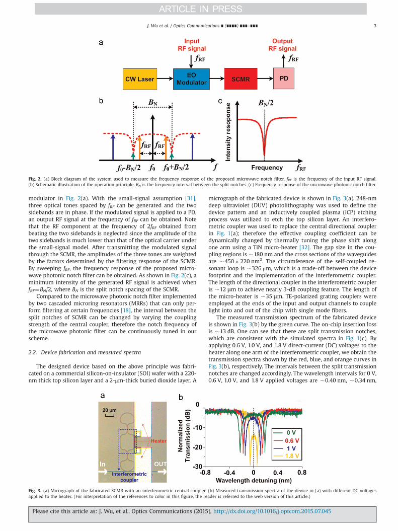
Fig. 2. (a) Block diagram of the system used to measure the frequency response of the proposed microwave notch filter. fRF is the frequency of the input RF signal.(b) Schematic illustration of the operation principle. BN is the frequency interval between the split notches. (c) Frequency response of the microwave photonic notch filter.
J. Wu et al. / Optics Communications ∎ (∎∎∎∎) ∎∎∎–∎∎∎ 3
modulator in Fig. 2(a). With the small-signal assumption [31],three optical tones spaced by fRF can be generated and the twosidebands are in phase. If the modulated signal is applied to a PD,an output RF signal at the frequency of fRF can be obtained. Notethat the RF component at the frequency of 2fRF obtained frombeating the two sidebands is neglected since the amplitude of thetwo sidebands is much lower than that of the optical carrier underthe small-signal model. After transmitting the modulated signalthrough the SCMR, the amplitudes of the three tones are weightedby the factors determined by the filtering response of the SCMR.By sweeping fRF, the frequency response of the proposed micro-wave photonic notch filter can be obtained. As shown in Fig. 2(c), aminimum intensity of the generated RF signal is achieved whenfRF¼BN/2, where BN is the split notch spacing of the SCMR.
Compared to the microwave photonic notch filter implementedby two cascaded microring resonators (MRRs) that can only per-form filtering at certain frequencies [18], the interval between thesplit notches of SCMR can be changed by varying the couplingstrength of the central coupler, therefore the notch frequency ofthe microwave photonic filter can be continuously tuned in ourscheme.
2.2. Device fabrication and measured spectra
The designed device based on the above principle was fabri-cated on a commercial silicon-on-insulator (SOI) wafer with a 220-nm thick top silicon layer and a 2-mm-thick buried dioxide layer. A
Fig. 3. (a) Micrograph of the fabricated SCMR with an interferometric central coupler.applied to the heater. (For interpretation of the references to color in this figure, the re
Please cite this article as: J. Wu, et al., Optics Communications (2015
micrograph of the fabricated device is shown in Fig. 3(a). 248-nmdeep ultraviolet (DUV) photolithography was used to define thedevice pattern and an inductively coupled plasma (ICP) etchingprocess was utilized to etch the top silicon layer. An interfero-metric coupler was used to replace the central directional couplerin Fig. 1(a); therefore the effective coupling coefficient can bedynamically changed by thermally tuning the phase shift alongone arm using a TiN micro-heater [32]. The gap size in the cou-pling regions is �180 nm and the cross sections of the waveguidesare �450�220 nm2. The circumference of the self-coupled re-sonant loop is �326 mm, which is a trade-off between the devicefootprint and the implementation of the interferometric coupler.The length of the directional coupler in the interferometric coupleris �12 μm to achieve nearly 3-dB coupling feature. The length ofthe micro-heater is �35 μm. TE-polarized grating couplers wereemployed at the ends of the input and output channels to couplelight into and out of the chip with single mode fibers.
The measured transmission spectrum of the fabricated deviceis shown in Fig. 3(b) by the green curve. The on-chip insertion lossis �13 dB. One can see that there are split transmission notches,which are consistent with the simulated spectra in Fig. 1(c). Byapplying 0.6 V, 1.0 V, and 1.8 V direct-current (DC) voltages to theheater along one arm of the interferometric coupler, we obtain thetransmission spectra shown by the red, blue, and orange curves inFig. 3(b), respectively. The intervals between the split transmissionnotches are changed accordingly. The wavelength intervals for 0 V,0.6 V, 1.0 V, and 1.8 V applied voltages are �0.40 nm, �0.34 nm,
(b) Measured transmission spectra of the device in (a) with different DC voltagesader is referred to the web version of this article.)
), http://dx.doi.org/10.1016/j.optcom.2015.07.045i

Fig. 4. Experimental setup for system demonstration of tunable microwave notchfiltering. PC: polarization controller. EA: electrical amplifier. MZM: Mach–Zehndermodulator. EDFA: erbium-doped fiber amplifier. TOF: tunable optical filter. DUT:device under test. OSA: optical spectrum analyzer. VOA: variable optical attenuator.PD: photodetector. NA: network analyzer.
J. Wu et al. / Optics Communications ∎ (∎∎∎∎) ∎∎∎–∎∎∎4
�0.27 nm, and �0.10 nm, respectively, corresponding to fre-quency intervals of �50 GHz, �42 GHz, �34 GHz, and �13 GHz,respectively. Note that the applied voltage also induces slightredshift of the transmission spectra, the symmetric axes of thethree spectra in Fig. 3(b) are aligned for comparisons of the tuningeffect. By further increasing the applied voltage, the spectral rangebetween the split notches decreases until the split notches finallymerge to a single one with increased depth. Theoretically, there isa maximum insertion loss if t2¼κ2, and the insertion loss increaseswith the increased voltage as a result of decreased couplingstrength of the central coupler. But the change of the insertion lossis so small that one cannot observe obvious difference in theexperiment.
2.3. System demonstration of the tunable microwave photonic notchfilter
We use the experimental setup shown in Fig. 4 to test theperformance of the fabricated device as a tunable microwavephotonic notch filter. A CW light from a tunable laser with a tuningresolution of 0.001 nm is employed as an optical carrier. Thegenerated CW light is modulated using a MZM with a modulationbandwidth of 40 GHz. The MZM is driven by an RF signal from anetwork analyzer (NA) (Agilent N5247A) and biased at the linearregion. The NA used to sweep RF frequencies has a maximumbandwidth of 27 GHz. The modulated signal is boosted by an er-bium-doped fiber amplifier (EDFA), followed by a tunable opticalfilter (TOF) to suppress the amplified spontaneous emission (ASE)noise. A polarization controller (PC) is inserted before the deviceunder test (DUT) to minimize the coupling loss of the TE-polarizedgrating couplers. An optical isolator is employed to block the un-desired reflection from the DUT. The output signal from the DUT issplit into two parts by a fiber optic power splitter. One part is fed
Fig. 5. (a) Measured frequency responses of the proposed microwave photonic notch filtverses the applied DC voltage.
Please cite this article as: J. Wu, et al., Optics Communications (2015
into an optical spectrum analyzer (OSA), and the other part isamplified by another EDFA and converted to electrical signal by aPD before finally sent to the NA.
The measured frequency responses recorded by the NA areshown in Fig. 5(a). The DC voltages applied to the heater are thesame as those in Fig. 3(b). The wavelength of the CW light isslightly tuned to align with the symmetry axis of the split trans-mission notches when applying different DC voltages. From Fig. 5(a), it can be seen that the frequency responses show notch fil-tering shapes, which are in agreement with the predictions inFig. 2(c). The filtering notch exhibits increased asymmetry anddecreased rejection ratio as the notch frequency decreases, whichis mainly induced by the filtering shape of the SCMR as well asincreased phase difference at the split notches. The maximumrejection ratio is over 25 dB, and a wide tunable range over 20 GHzis obtained. The increased DC voltage leads to increased 3-dBbandwidth of the photonic notch filter. When the applied DCvoltage is changed from 0.6 V to 1.0 V, the corresponding 3-dBbandwidth of the filtering notch is increased from �8.4 GHz to�8.7 GHz, respectively. The 3-dB bandwidth of the notch filter isdetermined by the Q-factor of the split resonances and the wa-velength accuracy of the optical carrier. Reduced 3-dB bandwidthcan be achieved with lower waveguide propagation loss. Fig. 5(b) shows that the notch frequency of the microwave photonicfilter can be continuously tuned by changing the applied DC vol-tage. These experimental results verify the feasibility of the fab-ricated device as a tunable microwave photonic notch filter.
3. Photonic generation of MMW signal based on frequencyextraction using a SCMR
MMW generation is a key technique in the broadband wirelessaccess networks and radar systems [33]. Conventional photonicsystems to generate MMW mostly rely on discrete optoelectronicdevices [34,35] and fiber-based components [36]. These archi-tectures are usually bulky, costly, and lack of flexibility and stabi-lity. Photonic generations of MMW using silicon photonic devicesare promising to solve these problems, as they can provide re-duced system volume, low cost, and improved stability. Severalschemes for photonic MMW generations based on silicon deviceshave been demonstrated [13,14]. In the section, we propose andexperimentally demonstrate photonic MMW generation using acompact on-chip silicon SCMR. Base on frequency extracting usingthe drop port of the proposed device, MMW signal can be easilygenerated. The frequency of the generated MMW signal can betuned by changing the interval between the split resonances. Inthe experiment, we have demonstrated photonic generation of�39-GHz and �29-GHz MMW signals using the fabricateddevices.
er when the applied DC voltages are 0 V, 0.6 V, 1.0 V, and 1.8 V. (b) Notch frequency
), http://dx.doi.org/10.1016/j.optcom.2015.07.045i

Fig. 6. (a) Schematic configuration of the SCMR with a drop output. (b) Normalized transmission spectrum from port IN to port OUT of the device in (a). (c) Zoom-in view of(b) around one split resonance marked with dashed box for various coupling strength of the central coupler in (a). The dashed vertical line in (c) shows symmetry axis of thesplit transmission peaks. (d) Schematic illustration of the frequency extraction principle.
J. Wu et al. / Optics Communications ∎ (∎∎∎∎) ∎∎∎–∎∎∎ 5
3.1. Device configuration and operation principle
The schematic configuration of the silicon device used for thephotonic MMW generation is shown in Fig. 6(a), which is similarto that in Fig. 1(a) except that there is another bus waveguide sidecoupled to the top of the Sagnac reflector serving as a drop outputchannel. The normalized transmission spectrum for t1¼0.95 andt2¼0.97 is shown in Fig. 6(b). The other parameters are the sameas those used in the simulation of Fig. 1(b). There are also splitresonances with bimodal distribution induced by the mutualmode coupling. Different from the split transmission notches inFig. 1(b), there are split transmission peaks in Fig. 6(b). In Fig. 6(c),we plot the transmission spectra around one split resonance forvaried t2. It can be seen that tunable interval between the two splittransmission peaks can also be obtained by changing the couplingstrength of the central coupler. As shown in Fig. 6(d), MMW can begenerated by using the proposed silicon device to extract a pair oftones from an optical frequency comb and then beating them in aPD. The frequency of the generated MMW equals BP, which is thefrequency interval between the split transmission peaks. Sincevaried frequency interval between the split transmission peaks can
Fig. 7. (a) Micrograph of a fabricated SCMR with a drop output channel. (b) Measuredreferences to color in this figure, the reader is referred to the web version of this articl
Please cite this article as: J. Wu, et al., Optics Communications (2015
be obtained for different t2, the frequency of the generated MMWsignal can be changed accordingly.
3.2. Device fabrication and measured spectra
Similar to that in Section 2.2, a number of devices were fabri-cated on a commercial SOI wafer with a CMOS compatible fabri-cation process. The micrograph for one of the fabricated devices isshown in Fig. 7(a). The cross-sections of the waveguides are cho-sen to be �500�220 nm2 to reduce the waveguide transmissionloss, thus increasing the quality factor of the split resonance peaks.Since the round-trip phase shift of the self-coupled resonant loopis the sum of the phase shifts along the Sagnac loop and thebottom ring, the asymmetry of the fabricated SCMR would notaffect the performance of the device. In order to obtain differentfrequency intervals between the split resonances, we used twosamples labeled as A and B with slight different coupling lengthsof the central directional couplers, i.e., �3.5 mm and �3 mm, re-spectively. For both samples, the straight coupling lengths of thetop and bottom directional couplers are �2.5 mm. The measuredtransmission spectra of samples A and B are shown in Fig. 7(b) by
transmission spectra of two devices labeled as A and B. (For interpretation of thee.)
), http://dx.doi.org/10.1016/j.optcom.2015.07.045i
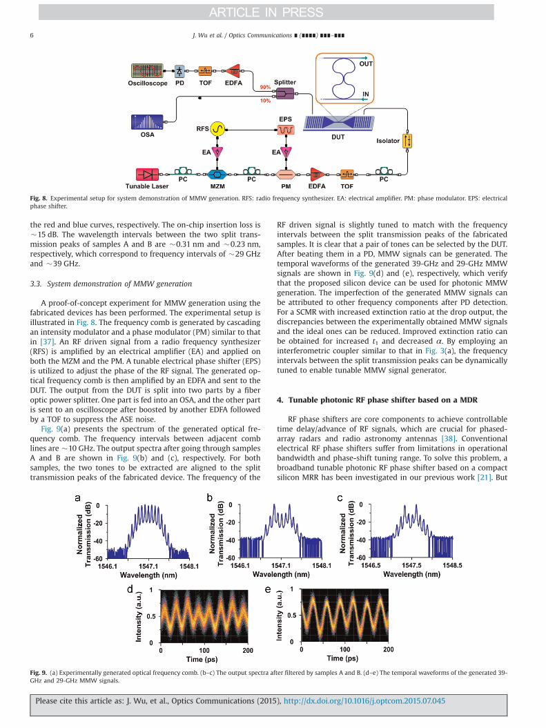
Fig. 8. Experimental setup for system demonstration of MMW generation. RFS: radio frequency synthesizer. EA: electrical amplifier. PM: phase modulator. EPS: electricalphase shifter.
J. Wu et al. / Optics Communications ∎ (∎∎∎∎) ∎∎∎–∎∎∎6
the red and blue curves, respectively. The on-chip insertion loss is�15 dB. The wavelength intervals between the two split trans-mission peaks of samples A and B are �0.31 nm and �0.23 nm,respectively, which correspond to frequency intervals of �29 GHzand �39 GHz.
3.3. System demonstration of MMW generation
A proof-of-concept experiment for MMW generation using thefabricated devices has been performed. The experimental setup isillustrated in Fig. 8. The frequency comb is generated by cascadingan intensity modulator and a phase modulator (PM) similar to thatin [37]. An RF driven signal from a radio frequency synthesizer(RFS) is amplified by an electrical amplifier (EA) and applied onboth the MZM and the PM. A tunable electrical phase shifter (EPS)is utilized to adjust the phase of the RF signal. The generated op-tical frequency comb is then amplified by an EDFA and sent to theDUT. The output from the DUT is split into two parts by a fiberoptic power splitter. One part is fed into an OSA, and the other partis sent to an oscilloscope after boosted by another EDFA followedby a TOF to suppress the ASE noise.
Fig. 9(a) presents the spectrum of the generated optical fre-quency comb. The frequency intervals between adjacent comblines are �10 GHz. The output spectra after going through samplesA and B are shown in Fig. 9(b) and (c), respectively. For bothsamples, the two tones to be extracted are aligned to the splittransmission peaks of the fabricated device. The frequency of the
Fig. 9. (a) Experimentally generated optical frequency comb. (b–c) The output spectra afGHz and 29-GHz MMW signals.
Please cite this article as: J. Wu, et al., Optics Communications (2015
RF driven signal is slightly tuned to match with the frequencyintervals between the split transmission peaks of the fabricatedsamples. It is clear that a pair of tones can be selected by the DUT.After beating them in a PD, MMW signals can be generated. Thetemporal waveforms of the generated 39-GHz and 29-GHz MMWsignals are shown in Fig. 9(d) and (e), respectively, which verifythat the proposed silicon device can be used for photonic MMWgeneration. The imperfection of the generated MMW signals canbe attributed to other frequency components after PD detection.For a SCMR with increased extinction ratio at the drop output, thediscrepancies between the experimentally obtained MMW signalsand the ideal ones can be reduced. Improved extinction ratio canbe obtained for increased t1 and decreased α. By employing aninterferometric coupler similar to that in Fig. 3(a), the frequencyintervals between the split transmission peaks can be dynamicallytuned to enable tunable MMW signal generator.
4. Tunable photonic RF phase shifter based on a MDR
RF phase shifters are core components to achieve controllabletime delay/advance of RF signals, which are crucial for phased-array radars and radio astronomy antennas [38]. Conventionalelectrical RF phase shifters suffer from limitations in operationalbandwidth and phase-shift tuning range. To solve this problem, abroadband tunable photonic RF phase shifter based on a compactsilicon MRR has been investigated in our previous work [21]. But
ter filtered by samples A and B. (d–e) The temporal waveforms of the generated 39-
), http://dx.doi.org/10.1016/j.optcom.2015.07.045i
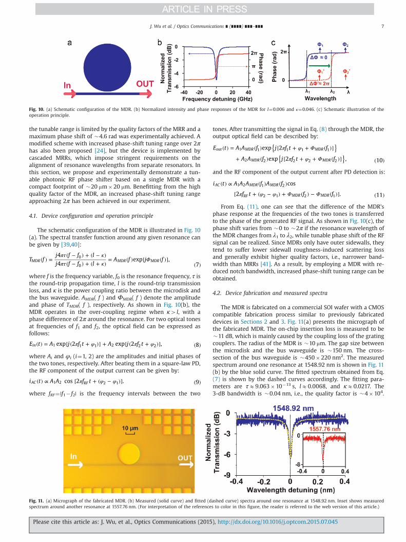
Fig. 10. (a) Schematic configuration of the MDR. (b) Normalized intensity and phase responses of the MDR for l¼0.006 and κ¼0.046. (c) Schematic illustration of theoperation principle.
J. Wu et al. / Optics Communications ∎ (∎∎∎∎) ∎∎∎–∎∎∎ 7
the tunable range is limited by the quality factors of the MRR and amaximum phase shift of �4.6 rad was experimentally achieved. Amodified scheme with increased phase-shift tuning range over 2πhas also been proposed [24], but the device is implemented bycascaded MRRs, which impose stringent requirements on thealignment of resonance wavelengths from separate resonators. Inthis section, we propose and experimentally demonstrate a tun-able photonic RF phase shifter based on a single MDR with acompact footprint of �20 mm�20 mm. Benefitting from the highquality factor of the MDR, an increased phase-shift tuning rangeapproaching 2π has been achieved in our experiment.
4.1. Device configuration and operation principle
The schematic configuration of the MDR is illustrated in Fig. 10(a). The spectral transfer function around any given resonance canbe given by [39,40]:
T fj f f l
j f f lA f j f
4
4exp ,
7MDR MDR MDR
0
0
πτ κπτ κ
Φ( ) =( − ) + ( − )( − ) + ( + )
= ( ) [ ( )]( )
where f is the frequency variable, f0 is the resonance frequency, τ isthe round-trip propagation time, l is the round-trip transmissionloss, and κ is the power coupling ratio between the microdisk andthe bus waveguide. AMDR( f ) and ΦMDR( f ) denote the amplitudeand phase of TMDR( f ), respectively. As shown in Fig. 10(b), theMDR operates in the over-coupling regime when κ4 l, with aphase difference of 2π around the resonance. For two optical tonesat frequencies of f1 and f2, the optical field can be expressed asfollows:
E t A j f t A j f texp 2 exp 2 , 8in 1 1 1 2 2 2π φ π φ( ) = [ ( + )] + [ ( + )] ( )
where Ai and φi (i¼1, 2) are the amplitudes and initial phases ofthe two tones, respectively. After beating them in a square-law PD,the RF component of the output current can be given by:
i t A A f tcos 2 . 9AC RF1 2 2 1π φ φ( ) ∝ [ + ( − )] ( )
where fRF¼ |f1� f2| is the frequency intervals between the two
Fig. 11. (a) Micrograph of the fabricated MDR. (b) Measured (solid curve) and fitted (dspectrum around another resonance at 1557.76 nm. (For interpretation of the reference
Please cite this article as: J. Wu, et al., Optics Communications (2015
tones. After transmitting the signal in Eq. (8) through the MDR, theoutput optical field can be described by:
E t A A f j f t f
A A f j f t f
exp 2
exp 2 , 10
out MDR MDR
MDR MDR
1 1 1 1 1
2 2 2 2 2
{ }{ }
π φ Φ
π φ Φ
( ) = ( ) [ + + ( )]
+ ( ) [ + + ( )] ( )
and the RF component of the output current after PD detection is:
i t A A A f A f
f t f f
cos
2 . 11
AC MDR MDR
RF MDR MDR
1 2 1 2
2 1 2 1π φ φ Φ Φ
( ) ∝ ( ) ( )
[ + ( − ) + ( ) − ( )] ( )
From Eq. (11), one can see that the difference of the MDR’sphase response at the frequencies of the two tones is transferredto the phase of the generated RF signal. As shown in Fig. 10(c), thephase shift varies from �0 to �2π if the resonance wavelength ofthe MDR changes from λ1 to λ2, while tunable phase shift of the RFsignal can be realized. Since MDRs only have outer sidewalls, theytend to suffer lower sidewall roughness-induced scattering lossand generally exhibit higher quality factors, i.e., narrower band-width than MRRs [41]. As a result, by employing a MDR with re-duced notch bandwidth, increased phase-shift tuning range can beobtained.
4.2. Device fabrication and measured spectra
The MDR is fabricated on a commercial SOI wafer with a CMOScompatible fabrication process similar to previously fabricateddevices in Sections 2 and 3. Fig. 11(a) presents the micrograph ofthe fabricated MDR. The on-chip insertion loss is measured to be�11 dB, which is mainly caused by the coupling loss of the gratingcouplers. The radius of the MDR is �10 mm. The gap size betweenthe microdisk and the bus waveguide is �150 nm. The cross-section of the bus waveguide is �450�220 nm2. The measuredspectrum around one resonance at 1548.92 nm is shown in Fig. 11(b) by the blue solid curve. The fitted spectrum obtained from Eq.(7) is shown by the dashed curves accordingly. The fitting para-meters are τE9.063�10�13 s, lE0.0068, and κE0.0217. The3-dB bandwidth is �0.04 nm, i.e., the quality factor is �4�104.
ashed curve) spectra around one resonance at 1548.92 nm. Inset shows measureds to color in this figure, the reader is referred to the web version of this article.)
), http://dx.doi.org/10.1016/j.optcom.2015.07.045i
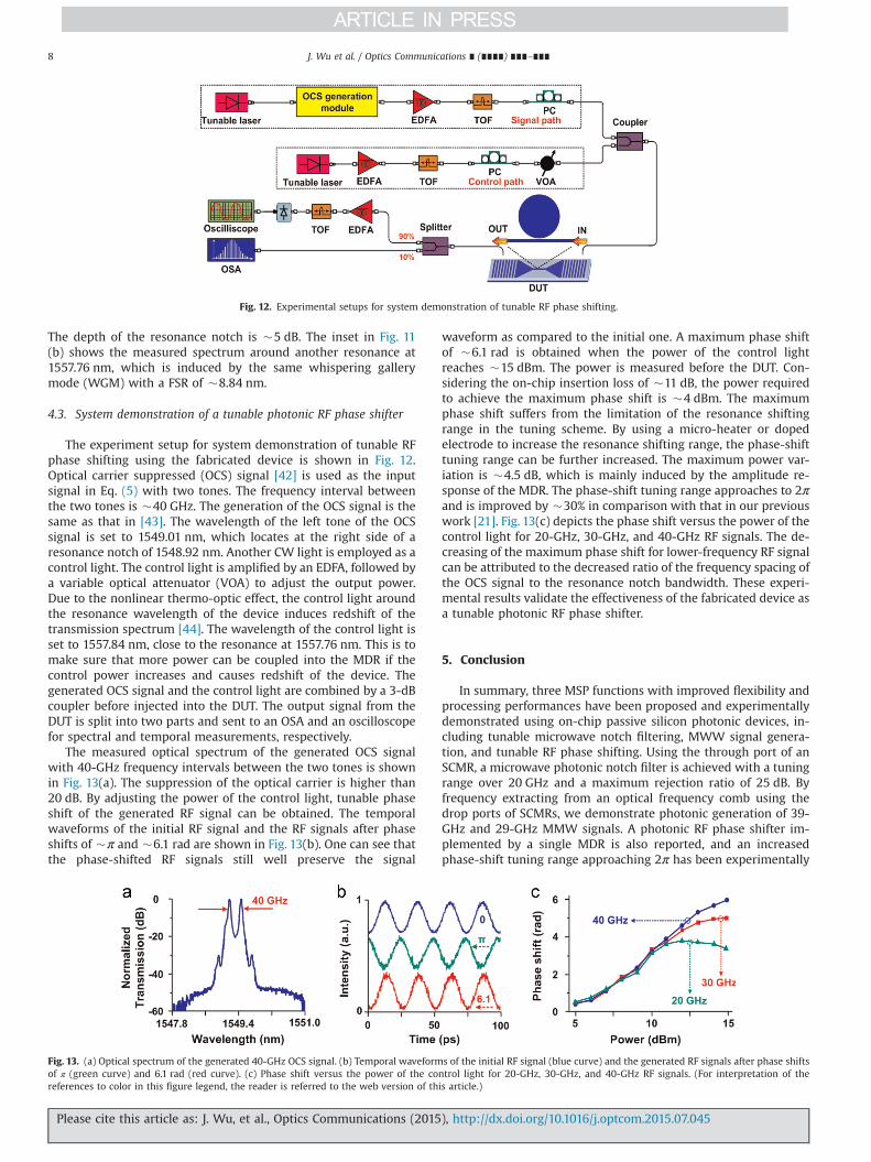
Fig. 12. Experimental setups for system demonstration of tunable RF phase shifting.
J. Wu et al. / Optics Communications ∎ (∎∎∎∎) ∎∎∎–∎∎∎8
The depth of the resonance notch is �5 dB. The inset in Fig. 11(b) shows the measured spectrum around another resonance at1557.76 nm, which is induced by the same whispering gallerymode (WGM) with a FSR of �8.84 nm.
4.3. System demonstration of a tunable photonic RF phase shifter
The experiment setup for system demonstration of tunable RFphase shifting using the fabricated device is shown in Fig. 12.Optical carrier suppressed (OCS) signal [42] is used as the inputsignal in Eq. (5) with two tones. The frequency interval betweenthe two tones is �40 GHz. The generation of the OCS signal is thesame as that in [43]. The wavelength of the left tone of the OCSsignal is set to 1549.01 nm, which locates at the right side of aresonance notch of 1548.92 nm. Another CW light is employed as acontrol light. The control light is amplified by an EDFA, followed bya variable optical attenuator (VOA) to adjust the output power.Due to the nonlinear thermo-optic effect, the control light aroundthe resonance wavelength of the device induces redshift of thetransmission spectrum [44]. The wavelength of the control light isset to 1557.84 nm, close to the resonance at 1557.76 nm. This is tomake sure that more power can be coupled into the MDR if thecontrol power increases and causes redshift of the device. Thegenerated OCS signal and the control light are combined by a 3-dBcoupler before injected into the DUT. The output signal from theDUT is split into two parts and sent to an OSA and an oscilloscopefor spectral and temporal measurements, respectively.
The measured optical spectrum of the generated OCS signalwith 40-GHz frequency intervals between the two tones is shownin Fig. 13(a). The suppression of the optical carrier is higher than20 dB. By adjusting the power of the control light, tunable phaseshift of the generated RF signal can be obtained. The temporalwaveforms of the initial RF signal and the RF signals after phaseshifts of �π and �6.1 rad are shown in Fig. 13(b). One can see thatthe phase-shifted RF signals still well preserve the signal
Fig. 13. (a) Optical spectrum of the generated 40-GHz OCS signal. (b) Temporal waveformof π (green curve) and 6.1 rad (red curve). (c) Phase shift versus the power of the coreferences to color in this figure legend, the reader is referred to the web version of th
Please cite this article as: J. Wu, et al., Optics Communications (2015
waveform as compared to the initial one. A maximum phase shiftof �6.1 rad is obtained when the power of the control lightreaches �15 dBm. The power is measured before the DUT. Con-sidering the on-chip insertion loss of �11 dB, the power requiredto achieve the maximum phase shift is �4 dBm. The maximumphase shift suffers from the limitation of the resonance shiftingrange in the tuning scheme. By using a micro-heater or dopedelectrode to increase the resonance shifting range, the phase-shifttuning range can be further increased. The maximum power var-iation is �4.5 dB, which is mainly induced by the amplitude re-sponse of the MDR. The phase-shift tuning range approaches to 2πand is improved by �30% in comparison with that in our previouswork [21]. Fig. 13(c) depicts the phase shift versus the power of thecontrol light for 20-GHz, 30-GHz, and 40-GHz RF signals. The de-creasing of the maximum phase shift for lower-frequency RF signalcan be attributed to the decreased ratio of the frequency spacing ofthe OCS signal to the resonance notch bandwidth. These experi-mental results validate the effectiveness of the fabricated device asa tunable photonic RF phase shifter.
5. Conclusion
In summary, three MSP functions with improved flexibility andprocessing performances have been proposed and experimentallydemonstrated using on-chip passive silicon photonic devices, in-cluding tunable microwave notch filtering, MWW signal genera-tion, and tunable RF phase shifting. Using the through port of anSCMR, a microwave photonic notch filter is achieved with a tuningrange over 20 GHz and a maximum rejection ratio of 25 dB. Byfrequency extracting from an optical frequency comb using thedrop ports of SCMRs, we demonstrate photonic generation of 39-GHz and 29-GHz MMW signals. A photonic RF phase shifter im-plemented by a single MDR is also reported, and an increasedphase-shift tuning range approaching 2π has been experimentally
s of the initial RF signal (blue curve) and the generated RF signals after phase shiftsntrol light for 20-GHz, 30-GHz, and 40-GHz RF signals. (For interpretation of theis article.)
), http://dx.doi.org/10.1016/j.optcom.2015.07.045i

J. Wu et al. / Optics Communications ∎ (∎∎∎∎) ∎∎∎–∎∎∎ 9
achieved. These silicon photonic devices are promising elementsfor future MSP systems.
Acknowledgments
This research was supported in part by the National NaturalScience Foundation of China under Grants 61125504/61235007,and in part by the 863 High-Tech Program under Grants2013AA013402/2015AA015503.
References
[1] A. Seeds, Microwave photonics, IEEE Trans. Microw. Theory Tech. 50 (2002)877–887.
[2] R. Minasian, Photonic signal processing of microwave signals, IEEE Trans.Microw. Theory Tech. 54 (2006) 832–846.
[3] J. Capmany, D. Novak, Microwave photonics combines two worlds, Nat. Pho-tonics 1 (2007) 319–330.
[4] J. Yao, Microwave photonics, J. Lightw. Technol. 27 (2009) 314–335.[5] D. Marpaung, C. Roeloffzen, R. Heideman, A. Leinse, S. Sales, J. Capmany, In-
tegrated microwave photonics, Laser Photonics Rev. 20 (2013) 1–30.[6] B. Jalali, S. Fathpour, Silicon photonics, J. Lightw. Technol. 24 (2006)
4600–4615.[7] M. Burla, L.R. Cortés, M. Li, X. Wang, L. Chrostowski, J. Azaña, Integrated wa-
veguide Bragg gratings for microwave photonics signal processing, Opt. Ex-press 21 (2013) 25120–25147.
[8] M. Khan, H. Shen, Y. Xuan, L. Zhao, S. Xiao, D. Leaird, A. Weiner, M. Qi, Ul-trabroad-bandwidth arbitrary radiofrequency waveform generation with asilicon photonic chip-based spectral shaper, Nat. Photonics 4 (2010) 117–122.
[9] H. Shen, M. Khan, L. Fan, L. Zhao, Y. Xuan, J. Ouyang, L. Varghese, M. Qi, Eight-channel reconfigurable microring filters with tunable frequency, extinctionratio and bandwidth, Opt. Express 18 (2010) 18067–18076.
[10] Y. Yue, H. Huang, L. Zhang, J. Wang, J. Yang, O. Yilmaz, J. Levy, M. Lipson,A. Willner, UWB monocycle pulse generation using two-photon absorption ina silicon waveguide, Opt. Lett. 37 (2012) 551–553.
[11] F. Liu, T. Wang, Z. Zhang, M. Qiu, Y. Su, On-chip photonic generation of ultra-wideband monocycle pulses, Electron. Lett. 45 (2009) 1–2.
[12] J. Li, H. Lee, K. Vahala, Microwave synthesizer using an on-chip Brillouin os-cillator, Nat. Commun. 4 (2013) 1–7.
[13] L. Xu, C. Li, C. Chow, H. Tsang, Optical mm-wave signal generation by fre-quency quadrupling using an optical modulator and a silicon microresonatorfilter, IEEE Photonics Technol. Lett. 21 (2009) 209–211.
[14] L. Liu, T. Yang, S. Liao, J. Dong, Photonic generation of millimeter-wave using asilicon microdisk resonator, Opt. Commun. 343 (2015) 115–120.
[15] M. Rasras, K. Tu, D. Gill, Y. Chen, A. White, S. Patel, A. Pomerene, D. Carothers,J. Beattie, M. Beals, J. Michel, L. Kimerling, Demonstration of a tunable mi-crowave-photonic notch filter using low-loss silicon ring resonators, J. Lightw.Technol. 27 (2009) 2105–2110.
[16] J. Palací, G. Villanueva, J. Galán, J. Martí, B. Vidal, Single bandpass photonicmicrowave filter based on a notch ring resonator, IEEE Photonics Technol. Lett.22 (2010) 1276–1278.
[17] D. Zhang, X. Feng, Y. Huang, Tunable and reconfigurable bandpass microwavephotonic filters utilizing integrated optical processor on silicon-on-insulatorsubstrate, IEEE Photonics Technol. Lett. 24 (2012) 1502–1505.
[18] J. Dong, L. Liu, D. Gao, Y. Yu, A. Zheng, T. Yang, X. Zhang, Compact notch mi-crowave photonic filters using on-chip integrated microring resonators, IEEEPhotonics J. 5 (2013) 5500307.
[19] P. Alipour, A. Eftekhar, A. Atabaki, Q. Li, S. Yegnanarayanan, C. Madsen,A. Adibi, Fully reconfigurable compact RF photonic filters using high-Q siliconmicrodisk resonators, Opt. Express 19 (2011) 15899–15907.
[20] W. Li, M. Li, J.P. Yao, A narrow-passband and frequency-tunable micro-wavephotonic filter based on phase-modulation to intensity-modulation
Please cite this article as: J. Wu, et al., Optics Communications (2015
conversion using a phase-shifted fiber Bragg grating, IEEE Trans. Microw.Theory Tech. 60 (2012) 1287–1296.
[21] Q. Chang, Q. Li, Z. Zhang, M. Qiu, T. Ye, Y. Su, A tunable broadband photonic RFphase shifter based on a silicon microring resonator, IEEE Photonics Technol.Lett. 21 (2009) 60–61.
[22] W. Xue, S. Sales, J. Capmany, J. Mørk, Microwave phase shifter with con-trollable power response based on slow- and fast-light effects in semi-conductor optical amplifiers, Opt. Lett. 34 (2009) 929–931.
[23] M. Pu, L. Liu, W. Xue, Y. Ding, L. Frandsen, H. Ou, K. Yvind, J. Hvam, Tunablemicrowave phase shifter based on silicon-on-insulator microring resonator,IEEE Photonics Technol. Lett. 22 (2010) 869–871.
[24] M. Pu, L. Liu, W. Xue, Y. Ding, H. Ou, K. Yvind, J. Hvam, Widely tunable mi-crowave phase shifter based on silicon-on-insulator dual-microring resonator,Opt. Express 18 (2010) 6172–6182.
[25] M. Li, Z. Li, J.P. Yao, Photonic generation of a precisely pi phase shifted binaryphase-coded microwave signal, IEEE Photonics Technol. Lett. 24 (2012)2001–2004.
[26] J. Capmany, B. Ortega, D. Pastor, A tutorial on microwave photonic filters, J.Lightw. Technol. 24 (2006) 201–299.
[27] E. Chan, R. Minasian, Multiple-tap, tunable microwave photonic interferencemitigation filter, J. Lightw. Technol. 29 (2011) 1069–1076.
[28] J. Ge, H. Feng, G. Scott, M. Fok, High-speed tunable microwave photonic notchfilter based on phase modulator incorporated Lyot filter, Opt. Lett. 40 (2015)48–51.
[29] Z. Zhang, M. Dainese, L. Wosinski, M. Qiu, Resonance-splitting and enhancednotch depth in SOI ring resonators with mutual mode coupling, Opt. Express16 (2008) 4621–4630.
[30] X. Sun, L. Zhou, J. Xie, Z. Zou, L. Lu, H. Zhu, X. Li, J. Chen, Tunable silicon Fabry–Perot comb filters formed by Sagnac loop mirrors, Opt. Lett. 38 (2013)567–569.
[31] J. Yao, F. Zeng, Q. Wang, Photonic generation of ultrawideband signals, J.Lightw. Technol. 25 (2007) 3219–3235.
[32] J. Wu, P. Cao, X. Hu, X. Jiang, T. Pan, Y. Yang, C. Qiu, C. Tremblay, Y. Su, Compacttunable silicon photonic differential-equation solver for general linear time-invariant systems, Opt. Express 22 (2014) 26254–26264.
[33] Z. Jia, J. Yu, G. Ellinas, G. Chang, Key enabling technologies for optical–wirelessnetworks: optical millimeter-wave generation, wavelength reuse, and archi-tecture, J. Lightw. Technol. 25 (2007) 3452–3471.
[34] J. Yu, Z. Jia, L. Yi, Y. Su, G.K. Chang, T. Wang, Optical millimeter-wave genera-tion or up-conversion using external modulators, IEEE Photonics Technol. Lett.18 (2006) 265–267.
[35] J. Yu, Z. Jia, T. Wang, G.K. Chang, A novel radio-over-fiber configuration usingoptical phase modulator to generate an optical mm-wave and centralizedlightwave for uplink connection, IEEE Photonics Technol. Lett. 19 (2007)140–142.
[36] L. Xia, P. Shum, T. Cheng, Photonic generation of microwave signals using adual-transmission-band FBG filter with controllable wavelength spacing, Appl.Phys. B 86 (2007) 61–64.
[37] M. Fujiwara, M. Teshima, J. Kani, H. Suzuki, N. Takachio, K. Iwatsuki, Opticalcarrier supply module using flattened optical multicarrier generation based onsinusoidal amplitude and phase hybrid modulation, J. Lightw. Technol. 21(2003) 2705–2714.
[38] R. Hansen, Phased Array Antennas, J. Wiley & Sons, Hoboken, New Jersey,2009.
[39] M. Lee, Tunable coupling regimes of silicon microdisk resonators using MEMSactuators, Opt. Express 14 (2006) 4703–4712.
[40] M. Soltani, S. Yegnanarayanan, A. Adibi, Ultra-high Q planar silicon microdiskresonators for chip-scale silicon photonics, Opt. Express 15 (2007) 4694–4704.
[41] S. Feng, T. Lei, H. Chen, H. Cai, X. Luo, A. Poon, Silicon photonics: from a mi-croresonator perspective, Laser Photonics Rev. 6 (2012) 145–177.
[42] P. Winzer, R. Essiambre, Advanced optical modulation formats, Proc. IEEE 94(2006) 952–985.
[43] Q. Chang, Y. Tian, J. Gao, T. Ye, Q. Li, Y. Su, Generation and transmission ofoptical carrier suppressed-optical differential (quadrature) phase-shift keying(OCS-OD(Q)PSK) signals in radio over fiber systems, J. Lightw. Technol. 26(2008) 2611–2618.
[44] F. Liu, Q. Li, Z. Zhang, M. Qiu, Y. Su, Optically tunable delay line in siliconmicroring resonator based on thermal nonlinear effect, IEEE J. Sel. Top.Quantum Electron. 14 (2008) 706–712.
), http://dx.doi.org/10.1016/j.optcom.2015.07.045i