Embed Size (px)
Citation preview

NCD - Master MIRI 1
Memory Structures
Ramon CanalNCD - Master MIRI
Slides based on:Introduction to CMOS VLSI Design. D. Harris

NCD - Master MIRI 2
Outline• Memory Arrays• SRAM Architecture
– SRAM Cell– Decoders– Column Circuitry– Multiple Ports
• Serial Access Memories

NCD - Master MIRI 3
Memory ArraysMemory Arrays
Random Access Memory Serial Access Memory Content Addressable Memory(CAM)
Read/Write Memory(RAM)
(Volatile)
Read Only Memory(ROM)
(Nonvolatile)
Static RAM(SRAM)
Dynamic RAM(DRAM)
Shift Registers Queues
First InFirst Out(FIFO)
Last InFirst Out(LIFO)
Serial InParallel Out
(SIPO)
Parallel InSerial Out
(PISO)
Mask ROM ProgrammableROM
(PROM)
ErasableProgrammable
ROM(EPROM)
ElectricallyErasable
ProgrammableROM
(EEPROM)
Flash ROM

NCD - Master MIRI 4
Array Architecture• 2n words of 2m bits each• If n >> m, fold by 2k into fewer rows of more columns
• Good regularity – easy to design• Very high density if good cells are used
row decoder
columndecoder
n
n-kk
2m bits
columncircuitry
bitline conditioning
memory cells:2n-k rows x2m+k columns
bitlines
wordlines

NCD - Master MIRI 5
12T SRAM Cell• Basic building block: SRAM Cell
– Holds one bit of information, like a latch– Must be read and written
• 12-transistor (12T) SRAM cell– Use a simple latch connected to bitline– 46 x 75 unit cell
bit
write
write_b
read
read_b

NCD - Master MIRI 6
6T SRAM Cell• Cell size accounts for most of array size
– Reduce cell size at expense of complexity• 6T SRAM Cell
– Used in most commercial chips– Data stored in cross-coupled inverters
• Read:– Precharge bit, bit_b– Raise wordline
• Write:– Drive data onto bit, bit_b– Raise wordline
bit bit_b
word

NCD - Master MIRI 7
SRAM Read• Precharge both bitlines high• Then turn on wordline• One of the two bitlines will be pulled down by the cell• Ex: A = 0, A_b = 1
– bit discharges, bit_b stays high– But A bumps up slightly
• Read stability– A must not flip
bit bit_b
N1
N2P1
A
P2
N3
N4
A_b
word
0.0
0.5
1.0
1.5
0 100 200 300 400 500 600time (ps)
word bit
A
A_b bit_b

NCD - Master MIRI 8
SRAM Read• Precharge both bitlines high• Then turn on wordline• One of the two bitlines will be pulled down by the cell• Ex: A = 0, A_b = 1
– bit discharges, bit_b stays high– But A bumps up slightly
• Read stability– A must not flip– N1 >> N2
bit bit_b
N1
N2P1
A
P2
N3
N4
A_b
word
0.0
0.5
1.0
1.5
0 100 200 300 400 500 600time (ps)
word bit
A
A_b bit_b

NCD - Master MIRI 9
SRAM Write• Drive one bitline high, the other low• Then turn on wordline• Bitlines overpower cell with new value• Ex: A = 0, A_b = 1, bit = 1, bit_b = 0
– Force A_b low, then A rises high
• Writability– Must overpower feedback inverter
time (ps)
word
A
A_b
bit_b
0.0
0.5
1.0
1.5
0 100 200 300 400 500 600 700
bit bit_b
N1
N2P1
A
P2
N3
N4
A_b
word
NCD - Master MIRI 10
SRAM Write• Drive one bitline high, the other low• Then turn on wordline• Bitlines overpower cell with new value• Ex: A = 0, A_b = 1, bit = 1, bit_b = 0
– Force A_b low, then A rises high
• Writability– Must overpower feedback inverter– N2 >> P1
time (ps)
word
A
A_b
bit_b
0.0
0.5
1.0
1.5
0 100 200 300 400 500 600 700
bit bit_b
N1
N2P1
A
P2
N3
N4
A_b
word

NCD - Master MIRI 11
SRAM Sizing• High bitlines must not overpower inverters during reads• But low bitlines must write new value into cell
bit bit_b
med
A
weak
strong
med
A_b
word
NCD - Master MIRI 12
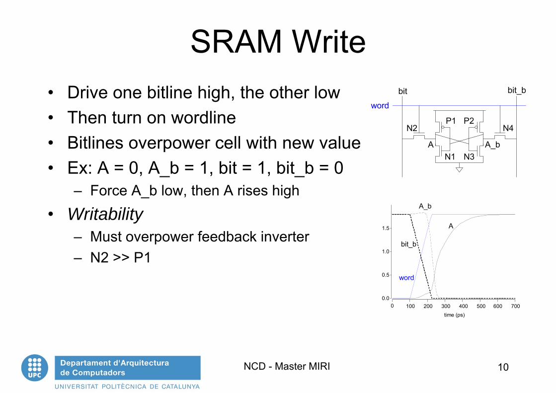
SRAM Column ExampleRead Write
H H
SRAM Cell
word_q1
bit_v1f
bit_b_v1f
out_v1rout_b_v1r
1
2
word_q1
bit_v1f
out_v1r
2
MoreCells
Bitline Conditioning
2
MoreCells
SRAM Cell
word_q1
bit_v1f
bit_b_v1f
data_s1
write_q1
Bitline Conditioning

NCD - Master MIRI 13
SRAM Layout
• Cell size is critical: 26 x 45 (even smaller in industry)• Tile cells sharing VDD, GND, bitline contacts
VDD
GND GNDBIT BIT_B
WORD
Cell boundary

NCD - Master MIRI 14
Periphery
Decoders Sense Amplifiers Input/Output Buffers Control / Timing Circuitry

NCD - Master MIRI 15
Decoders• n:2n decoder consists of 2n n-input AND gates
– One needed for each row of memory– Build AND from NAND or NOR gates
Static CMOS Pseudo-nMOS
word0
word1
word2
word3
A0A1
A1word
A0 1 1
1/2
2
4
8
16word
A0
A1
11
11
4
8
word0
word1
word2
word3
A0A1

NCD - Master MIRI 16
Decoder Layout• Decoders must be pitch-matched to SRAM cell
– Requires very skinny gates
GND
VDD
word
buffer inverterNAND gate
A0A0A1A2A3 A2A3 A1

NCD - Master MIRI 17
Large Decoders• For n > 4, NAND gates become slow
– Break large gates into multiple smaller gates
word0
word1
word2
word3
word15
A0A1A2A3

NCD - Master MIRI 18
Predecoding• Many of these gates are redundant
– Factor out commongates into predecoder
– Saves area– Same path effort
A0
A1
A2
A3
word1
word2
word3
word15
word0
1 of 4 hotpredecoded lines
predecoders

NCD - Master MIRI 19
Periphery
Decoders Sense Amplifiers Input/Output Buffers Control / Timing Circuitry

NCD - Master MIRI 20
Sense Amplifiers
tpC V
Iav----------------=
make V as smallas possible
smalllarge
Idea: Use Sense Amplifer
outputinput
s.a.smalltransition
NCD - Master MIRI 21
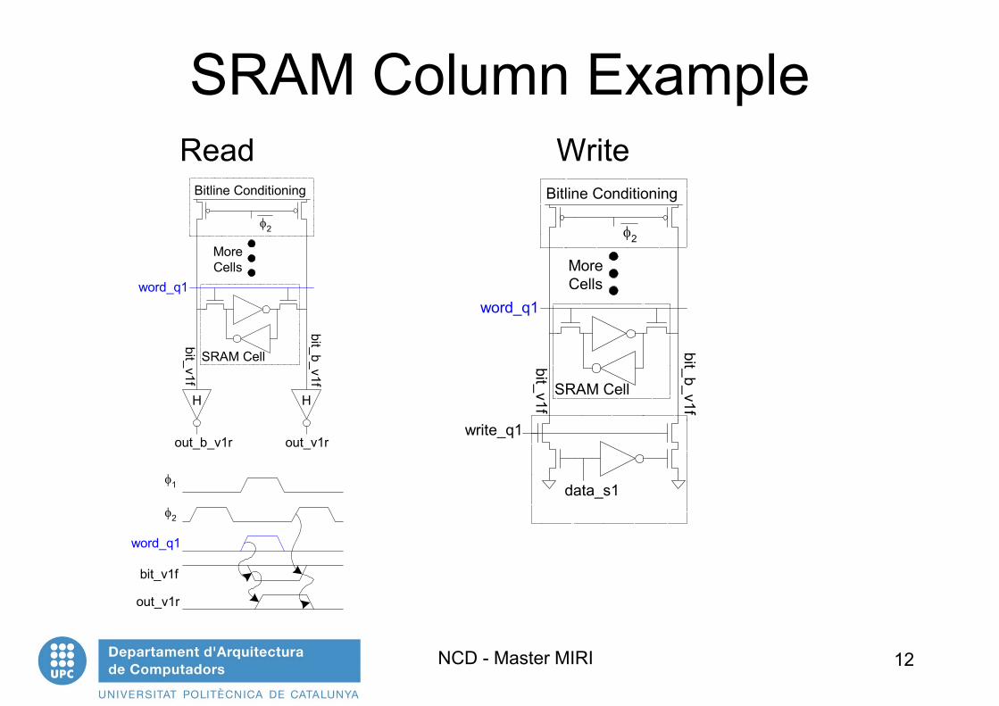
Sense Amplifiers• Bitlines have many cells attached
– Ex: 32-kbit SRAM has 256 rows x 128 cols– 128 cells on each bitline
• tpd (C/I) V– Even with shared diffusion contacts, 64C of diffusion
capacitance (big C)– Discharged slowly through small transistors (small I)
• Sense amplifiers are triggered on small voltage swing (reduce V)

NCD - Master MIRI 22
Differential Pair Amp• Differential pair requires no clock• But always dissipates static power
bit bit_bsense_b sense
N1 N2
N3
P1 P2
NCD - Master MIRI 23
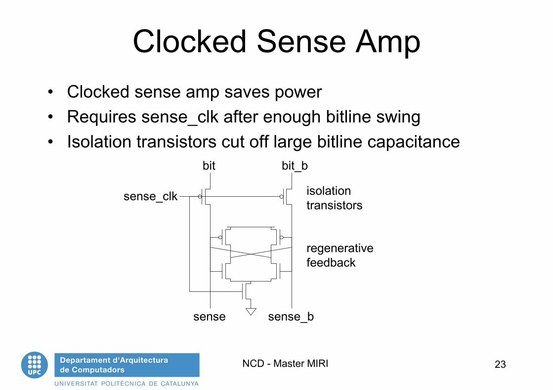
Clocked Sense Amp• Clocked sense amp saves power• Requires sense_clk after enough bitline swing• Isolation transistors cut off large bitline capacitance
bit_bbit
sense sense_b
sense_clk isolationtransistors
regenerativefeedback

NCD - Master MIRI 24
Periphery
Decoders Sense Amplifiers Input/Output Buffers Control / Timing Circuitry

NCD - Master MIRI 25
Column Circuitry• Some circuitry is required for each column
– Bitline conditioning– Column multiplexing

NCD - Master MIRI 26
Bitline Conditioning• Precharge bitlines high before reads
• Equalize bitlines to minimize voltage difference when using sense amplifiers
bit bit_b
bit bit_b

NCD - Master MIRI 27
Twisted Bitlines• Sense amplifiers also amplify noise
– Coupling noise is severe in modern processes– Try to couple equally onto bit and bit_b– Done by twisting bitlines
b0 b0_b b1 b1_b b2 b2_b b3 b3_b

NCD - Master MIRI 28
Column Multiplexing• Recall that array may be folded for good aspect ratio• Ex: 2 kword x 16 folded into 256 rows x 128 columns
– Must select 16 output bits from the 128 columns– Requires 16 8:1 column multiplexers

NCD - Master MIRI 29
Tree Decoder Mux• Column mux can use pass transistors
– Use nMOS only, precharge outputs
• One design is to use k series transistors for 2k:1 mux– No external decoder logic needed
B0 B1 B2 B3 B4 B5 B6 B7 B0 B1 B2 B3 B4 B5 B6 B7A0
A0
A1
A1
A2
A2
Y Yto sense amps and write circuits

NCD - Master MIRI 30
Single Pass-Gate Mux• Or eliminate series transistors with separate decoder
A0A1
B0 B1 B2 B3
Y

NCD - Master MIRI 31
Ex: 2-way Muxed SRAM
MoreCells
word_q1
write0_q1
2
MoreCells
A0
A0
2
data_v1
write1_q1
NCD - Master MIRI 32
Memory configuratons
Multiported memories CAM Memories Serial Access, Queues

NCD - Master MIRI 33
Multiple Ports• We have considered single-ported SRAM
– One read or one write on each cycle
• Multiported SRAM are needed for register files• Examples:
– Multicycle processor must read two sources or write a result on some cycles
– Pipelined processor must read two sources and write a third result each cycle
– Superscalar processor must read and write many sources and results each cycle

NCD - Master MIRI 34
Dual-Ported SRAM• Simple dual-ported SRAM
– Two independent single-ended reads– Or one differential write
• Do two reads and one write by time multiplexing– Read during ph1, write during ph2
bit bit_b
wordBwordA

NCD - Master MIRI 35
Multi-Ported SRAM• Adding more access transistors hurts read stability• Multiported SRAM isolates reads from state node• Single-ended design minimizes number of bitlines
bA
wordBwordA
wordDwordC
wordFwordE
wordG
bB bC
writecircuits
readcircuits
bD bE bF bG

NCD - Master MIRI 36
Memory configuratons
Multiported memories CAM Memories Serial Access, Queues

NCD - Master MIRI 37
Contents-Addressable Memory
Add
ress
Dec
oder
Data (64 bits)
I/O B
uffe
rs
Comparand
CAM Array29 words 3 64 bits
Mask
Control Logic R/W Address (9 bits)
Com
man
ds
29 Val
idity
Bits
Prio
rity
Enc
oder

NCD - Master MIRI 38
Memory configuratons
Multiported memories CAM Memories Serial Access, Queues

NCD - Master MIRI 39
Serial Access Memories• Serial access memories do not use an address
– Shift Registers– Tapped Delay Lines– Serial In Parallel Out (SIPO)– Parallel In Serial Out (PISO)– Queues (FIFO, LIFO)

NCD - Master MIRI 40
Shift Register• Shift registers store and delay data• Simple design: cascade of registers
– Watch your hold times!
clk
Din Dout8

NCD - Master MIRI 41
Denser Shift Registers• Flip-flops aren’t very area-efficient• For large shift registers, keep data in SRAM instead• Move read/write pointers to RAM rather than data
– Initialize read address to first entry, write to last– Increment address on each cycle
Din
Dout
clk
counter counterreset
00...00
11...11
readaddr
writeaddr
dual-portedSRAM

NCD - Master MIRI 42
Tapped Delay Line• A tapped delay line is a shift register with a
programmable number of stages• Set number of stages with delay controls to mux
– Ex: 0 – 63 stages of delay
SR
32
clk
Din
delay5
SR
16
delay4
SR
8
delay3S
R4
delay2
SR
2
delay1
SR
1
delay0
Dout
NCD - Master MIRI 43
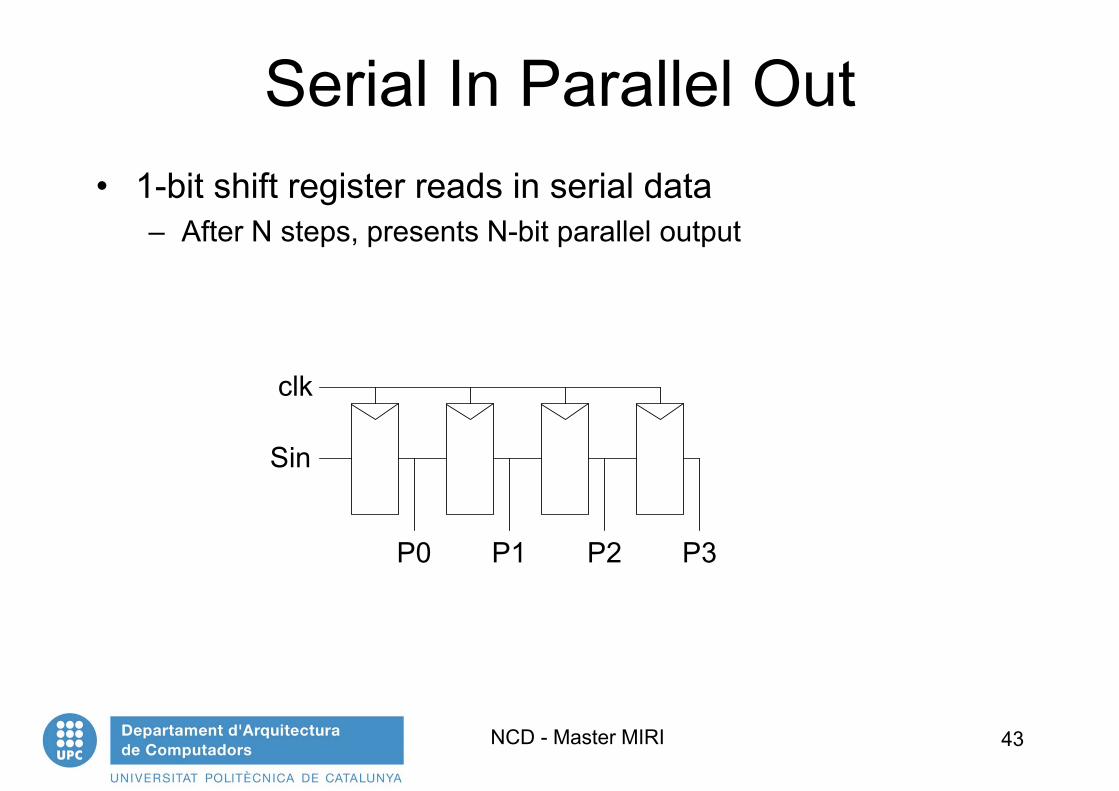
Serial In Parallel Out• 1-bit shift register reads in serial data
– After N steps, presents N-bit parallel output
clk
P0 P1 P2 P3
Sin

NCD - Master MIRI 44
Parallel In Serial Out• Load all N bits in parallel when shift = 0
– Then shift one bit out per cycle
clkshift/load
P0 P1 P2 P3
Sout

NCD - Master MIRI 45
Queues• Queues allow data to be read and written at different
rates.• Read and write each use their own clock, data• Queue indicates whether it is full or empty• Build with SRAM and read/write counters (pointers)
Queue
WriteClk
WriteData
FULL
ReadClk
ReadData
EMPTY

NCD - Master MIRI 46
FIFO, LIFO Queues• First In First Out (FIFO)
– Initialize read and write pointers to first element– Queue is EMPTY– On write, increment write pointer– If write almost catches read, Queue is FULL– On read, increment read pointer
• Last In First Out (LIFO)– Also called a stack– Use a single stack pointer for read and write

NCD - Master MIRI 47
Other considerations
Leakage control Redundancy Flash Memories

NCD - Master MIRI 48
Suppressing Leakage in SRAM
SRAMcell
SRAMcell
SRAMcell
VDD,int
VDDVDD VDDL
VSS,int
sleep
sleep
SRAMcell
SRAMcell
SRAMcell
VDD,int
sleep
low-threshold transistor
Reducing the supply voltageInserting Extra Resistance

NCD - Master MIRI 49
Other considerations
Leakage control Redundancy Flash Memories

NCD - Master MIRI 50
Redundancy
MemoryArray
Column Decoder
Row Decoder
Redundantrows
Redundantcolumns
RowAddress
ColumnAddress
FuseBank:

NCD - Master MIRI 51
Error-Correcting CodesExample: Hamming Codes
with
e.g. B3 Wrong
1
1
0
= 3

NCD - Master MIRI 52
Redundancy and Error Correction

NCD - Master MIRI 53
Other considerations
Leakage control Redundancy Flash Memories

NCD - Master MIRI 54
Flash EEPROM
Control gate
erasure
p-substrate
Floating gate
Thin tunneling oxide
n 1 source n1 drainprogramming
Many other options …

NCD - Master MIRI 55
Cross-sections of NVM cells
EPROMFlashCourtesy Intel

NCD - Master MIRI 56
Basic Operations in a NOR Flash Memory―
Erase
S D
12 VG
cell arrayBL 0 BL 1
open open
WL 0
WL 1
0 V
0 V
12 V

NCD - Master MIRI 57
Basic Operations in a NOR Flash Memory―
Write
S D
12 V
6 VG
BL 0 BL 1
6 V 0 V
WL 0
WL 1
12 V
0 V
0 V
NCD - Master MIRI 58
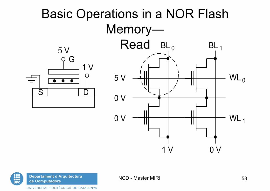
Basic Operations in a NOR Flash Memory―
Read5 V
1 VG
S D
BL 0 BL 1
1 V 0 V
WL 0
WL 1
5 V
0 V
0 V

NCD - Master MIRI 59
Row
Dec
oder
Bit line2L 2 K
Word line
AK
AK1 1
AL 2 1
A0
M.2K
AK2 1
Sense amplifiers / Drivers
Column decoder
Input-Output(M bits)
Storage cell
ConclusionsMemory Structure:
Amplify swing torail-to-rail amplitude
Selects appropriateword