Embed Size (px)
Citation preview

General DescriptionThe MAX3293/MAX3294/MAX3295 low-power, high-speed transmitters for RS-485/RS-422 commu-nication operate from a single +3.3V power supply. These devices contain one differential transmitter. The MAX3295 transmitter operates at data rates up to 20Mbps, with an output skew of less than 5ns, and a guaranteed driver propagation delay below 25ns. The MAX3293 (250kbps) and MAX3294 (2.5Mbps) are slew-rate limited to minimize EMI and reduce reflections caused by improperly terminated cables.The MAX3293/MAX3294/MAX3295 output level is guar-anteed at +1.5V with a standard 54Ω load, compliant with RS-485 specifications. The transmitter draws 5mA of supply current when unloaded, and 1µA in low-power shutdown mode (DE = GND).Hot-swap circuitry eliminates false transitions on the data cable during circuit initialization or connection to a live backplane, and short-circuit current limiting and ther-mal-shutdown circuitry protect the driver against exces-sive power dissipation.The MAX3293/MAX3294/MAX3295 are offered in a 6-pin SOT23 package, and are specified over the automotive temperature range.
Applications RS-485/RS-422 Communications Clock Distribution Telecom Equipment Automotive Security Equipment Point-of-Sale Equipment Industrial Control
Features Space-Saving 6-Pin SOT23 Package 250kbps/2.5Mbps/20Mbps Data Rates Available Operate from a Single +3.3V Supply ESD Protection
±9kV–Human Body Model Slew-Rate Limited for Errorless Data Transmission
(MAX3293/MAX3294) 1µA Low-Current Shutdown Mode -7V to +12V Common-Mode Input Voltage Range Current Limiting and Thermal Shutdown for
Driver-Overload Protection Hot-Swap Inputs for Telecom Applications Automotive Temperature Range (-40°C to +125°C)
Pin Configuration appears at end of data sheet.
+Denotes a lead(Pb)-free/RoHS-compliant package. T = Tape and reel. /V denotes automotive-qualified package.
PARTMAXIMUM
DATA RATE(Mbps)
SLEW-RATE
LIMITEDTOP
MARK
MAX3293AUT+T 0.25 Yes ABNI or ABVH
MAX3294AUT+T 2.5 Yes ABNJ or ABVI
MAX3295AUT+T 20 No ABNK or ABVJ
MAX3295AUT/V+T 20 No +ACSB
PART TEMP RANGE PIN-PACKAGEMAX3293AUT+T -40°C to +125°C 6 SOT23-6
MAX3294AUT+T -40°C to +125°C 6 SOT23-6
MAX3295AUT+T -40°C to +125°C 6 SOT23-6
MAX3295AUT/V+T -40°C to +125°C 6 SOT23-6
MAX3293MAX3294MAX3295
DDI
DE
MAX3280EMAX3281EMAX3283EMAX3284E
R RO
120ΩZ
Y
MAX3293–MAX3295 20Mbps, +3.3V, SOT23 RS-485/RS-422 Transmitters
19-2770; Rev 4; 12/14
Selector Guide
Ordering Information
Typical Operating Circuit

(All voltages referenced to GND, unless otherwise noted.)Supply Voltage (VCC) ............................................................+6VDE, DI ......................................................................-0.3V to +6VY, Z ........................................................................-7V to +12.5VMaximum Continuous Power Dissipation (TA = +70°C)
SOT23 (derate 8.2mW/°C above +70°C) .................654.1mW
Operating Temperature Ranges MAX32_ _AUT .............................................. -40°C to +125°C
Storage Temperature Range ............................ -65°C to +160°CJunction Temperature .....................................................+160°CLead Temperature (soldering, 10s) .................................+300°CSoldering Temperature (reflow) .......................................+260°C
(VCC = +3.3V ±5%, TA = TMIN to TMAX, unless otherwise noted. Typical values are at VCC = +3.3V and TA = +25°C.) (Notes 1, 2)
PARAMETER SYMBOL CONDITIONS MIN TYP MAX UNITSPOWER SUPPLYSupply Voltage VCC 3.135 3.300 3.465 VSupply Current in NormalOperation
IQ No load, DI = VCC or GND, DE = VCC 5 mA
Supply Current in Shutdown Mode ISHDN No load, DE = GND 1 10 µA
DRIVER
Differential Driver Output VODFigure 1, DE = VCC,DI = GND or VCC
R = 50Ω (RS-422),TA ≤ +85°C
2.0 VCCV
R = 27Ω (RS-485),TA ≤ +85°C
1.5 VCC
Change in Magnitude ofDifferential Output Voltage
∆VODFigure 1, R = 27Ω or 50Ω,DE = VCC (Note 3)
0.2 V
Driver Common-ModeOutput Voltage
VOCFigure 1, R = 27Ω or 50Ω,DE = VCC, DI = VCC or GND
-1 +3 V
Change in Magnitude ofCommon-Mode Voltage
∆VOC Figure 1, R = 27Ω or 50Ω (Note 3) 0.2 V
DRIVER LOGICInput High Voltage VIH DE, DI 2.0 V
Input Low Voltage VIL DE, DI 0.8 V
Input Current IIN DE, DI -2 +2 µA
Output Leakage IO
Y, ZDE = GND,VCC = GND or+3.3V
VIN = +12V -20 +20µA
VIN = -7V -20 +20
Driver Short-Circuit FoldbackOutput Current
IOSFD(VCC - 1V) ≤ VOUT ≤ +12V, output high +25
mA-7V ≤ VOUT ≤ 1V, output high -25
Driver Short-CircuitOutput Current
IOSD0 ≤ VOUT ≤ +12V, output low -250
mA-7V ≤ VOUT ≤ VCC, output high +250
Thermal-Shutdown Threshold TTS 160 °C
Thermal-Shutdown Hysteresis TTSH 40 °C
ESD Protection Y, Z Human Body Model ±9 kV
MAX3293–MAX3295 20Mbps, +3.3V, SOT23 RS-485/RS-422 Transmitters
www.maximintegrated.com Maxim Integrated 2
Electrical Characteristics
Stresses beyond those listed under “Absolute Maximum Ratings” may cause permanent damage to the device. These are stress ratings only, and functional operation of the device at these or any other conditions beyond those indicated in the operational sections of the specifications is not implied. Exposure to absolute maximum rating conditions for extended periods may affect device reliability.
Absolute Maximum Ratings

(VCC = +3.3V ±5%, TA = +25°C, unless otherwise noted. Typical values are at VCC = +3.3V.)
(VCC = +3.3V ±5%, TA = +25°C, unless otherwise noted. Typical values are at VCC = +3.3V.)
PARAMETER SYMBOL CONDITIONS MIN TYP MAX UNITS
Driver Propagation DelaytPLH Figures 2, 3; RDIFF = 54Ω,
CL = 50pF24 70
nstPHL 24 70
Driver Differential Output Rise orFall Time
tR Figures 2, 3; RDIFF = 54Ω,CL = 50pF
10 70ns
tF 10 70
Driver-Output Skew tSKEWFigures 2, 3; RDIFF = 54Ω, CL = 50pF,tSKEW = | tPLH - tPHL | (Note 5)
-40 +40 ns
Differential Driver-Output Skew tDSKEW Figures 2, 3; RDIFF = 54Ω, CL = 50pF -6 +6 ns
Maximum Data Rate Figures 2, 3; RDIFF = 54Ω, CL = 50pF 2.5 Mbps
Driver Enable to Output High tZHFigures 4, 5; S2 closed, RL = 500Ω,CL = 100pF
400 ns
Driver Enable to Output Low tZLFigures 4, 5; S1 closed, RL = 500Ω,CL = 100pF
400 ns
Driver Disable Time from Low tLZFigures 4, 5; S1 closed, RL = 500Ω,CL = 100pF
100 ns
Driver Disable Time from High tHZFigures 4, 5; S2 closed, RL = 500Ω,CL = 100pF
100 ns
Device-to-Device PropagationDelay Matching
Same power supply, maximum temperaturedifference between devices = +30°C (Note 5)
46 ns
PARAMETER SYMBOL CONDITIONS MIN TYP MAX UNITS
Driver Propagation DelaytPLH Figures 2, 3; RDIFF = 54Ω,
CL = 50pF400 1300
nstPHL 400 1300
Driver Differential Output Riseor Fall Time
tR Figures 2, 3; RDIFF = 54Ω,CL = 50pF
400 1200ns
tF 400 1200
Driver-Output Skew tSKEWFigures 2, 3; RDIFF = 54Ω, CL = 50pF,tSKEW = | tPLH - tPHL | (Note 5)
-400 +400 ns
Differential Driver-Output Skew tDSKEW Figures 2, 3; RDIFF = 54Ω, CL = 50pF -100 +100 ns
Maximum Data Rate Figures 2, 3; RDIFF = 54Ω, CL = 50pF 250 kbps
Driver Enable to Output High tZHFigures 4, 5; S2 closed, RL = 500Ω,CL = 100pF
2000 ns
Driver Enable to Output Low tZLFigures 4, 5; S1 closed, RL = 500Ω,CL = 100pF
2000 ns
Driver Disable Time from Low tLZFigures 4, 5; S1 closed, RL = 500Ω,CL = 100pF
1000 ns
Driver Disable Time from High tHZFigures 4, 5; S2 closed, RL = 500Ω,CL = 100pF
1000 ns
Device-to-Device PropagationDelay Matching
Same power supply, maximum temperaturedifference between devices = +30°C (Note 5)
900 ns
MAX3293–MAX3295 20Mbps, +3.3V, SOT23 RS-485/RS-422 Transmitters
www.maximintegrated.com Maxim Integrated 3
Switching Characteristics (MAX3294)
Switching Characteristics (MAX3293)

Note 1: Devices production tested at +25°C. Limits over the operating temperature range are guaranteed by design.Note 2: All currents into the device are positive; all currents out of the device are negative. All voltages are referenced to device
ground, unless otherwise noted.Note 3: ∆VOD and ∆VOC are the changes in VOD and VOC, respectively, when the DI input changes state.Note 4: The maximum current applies to peak current just prior to foldback current limiting.Note 5: Guaranteed by design; not production tested.
(VCC = +3.3V ±5%, TA = +25°C, unless otherwise noted. Typical values are at VCC = +3.3V.)
PARAMETER SYMBOL CONDITIONS MIN TYP MAX UNITS
Driver Propagation DelaytPLH Figures 2, 3; RDIFF = 54Ω, CL = 50pF
25ns
tPHL 25
Driver Differential Output Riseor Fall Time
tR Figures 2, 3;RDIFF = 54Ω,CL = 50pF
TA = -40°C to +125°C 18.5
nsTA < +85°C 15
tFTA = -40°C to +125°C 18.5
TA < +85°C 15
Driver-Output Skew tSKEWFigures 2, 3; RDIFF = 54Ω, CL = 50pF,tSKEW = | tPLH - tPHL |
5 ns
Differential Driver-Output Skew tDSKEW Figures 2, 3; RDIFF = 54Ω, CL = 50pF 5 ns
Maximum Data RateFigures 2, 3; RDIFF = 54Ω, CL = 50pF,TA ≤ +85°C
20Mbps
Figures 2, 3; RDIFF = 54Ω, CL = 50pF 16
Driver Enable to Output High tZHFigures 4, 5; S2 closed, RL = 500Ω,CL = 100pF
400 ns
Driver Enable to Output Low tZLFigures 4, 5; S1 closed, RL = 500Ω,CL = 100pF
400 ns
Driver Disable Time from Low tLZFigures 4, 5; S1 closed, RL = 500Ω,CL = 100pF
100 ns
Driver Disable Time from High tHZFigures 4, 5; S2 closed, RL = 500Ω,CL = 100pF
100 ns
Device-to-Device PropagationDelay Matching
Same power supply, maximum temperaturedifference between devices = +30°C (Note 5)
25 ns
MAX3293–MAX3295 20Mbps, +3.3V, SOT23 RS-485/RS-422 Transmitters
www.maximintegrated.com Maxim Integrated 4
Switching Characteristics (MAX3295)

Figure 5. Driver Enable and Disable Times
Figure 4. Enable/Disable Timing Test Load
Figure 3. Driver Propagation Delays
Figure 2. Driver Timing Test Circuit
Figure 1. Driver DC Test Load
OUTPUT NORMALLY LOW
OUTPUT NORMALLY HIGH
3V
0V
Y, Z
VOL
Y, Z
0V
1.5V 1.5V
VOL + 0.25V
VOH - 0.25V2.3V
2.3V
tZL(SHDN), tZL tLZ
tZH(SHDN), tZH tHZ
DE
S1
S2
OUTPUTUNDER TEST
VCC
CL
RL
DI3V
0V
Z
Y
VO0V
-VO
VO
1.5V
1/2 VO
1/2 VOtPLH
tFtR
tPHL
10%90% 90%
1.5V
10%
VDIFF = V (Y) - V (Z)
tSKEW = | tPLH - tPHL |
VDIFF
f = 1MHz, tR 3ns, tF 3ns
DI
DE
3V
YVID
CL
CL
RDIFF
Z
Y
Z
VOD
R
R VOC
MAX3293–MAX3295 20Mbps, +3.3V, SOT23 RS-485/RS-422 Transmitters
www.maximintegrated.com Maxim Integrated 5
Test Circuits and Timing Diagrams

(VCC = +3.3V, TA = +25°C, unless otherwise noted.)
0
10
20
30
40
MAX
3293
-95
toc0
9
TEMPERATURE (C)
PROP
AGAT
ION
DELA
Y (n
s)
-40 20 50 80-10 110
DRIVER PROPAGATION DELAYvs. TEMPERATURE
tPHL
tPLH
RDIFF = 54ΩCL = 50pF
0
1
2
3
4OUTPUT SKEW vs. TEMPERATURE
MAX
3293
-95
toc0
8
TEMPERATURE (C)
OUTP
UT S
KEW
(ns)
-40 20 50 80-10 110
DRIVER-OUTPUT CURRENT vs. DRIVER-OUTPUT HIGH VOLTAGE
MAX
3293
-95
toc0
7
OUTPUT HIGH VOLTAGE (V)
OUTP
UT C
URRE
NT (m
A)
0
-100
-40
-60
-80
-20
-120-7 -5 -3 -1 1 3 5
20
DRIVER-OUTPUT CURRENT vs. DRIVER-OUTPUT LOW VOLTAGE
MAX
3293
-95
toc0
6
OUTPUT LOW VOLTAGE (V)
OUTP
UT C
URRE
NT (m
A)
20
80
60
40
100
00 2 4 6 8 10 12
140
120
1.0
2.0
2.5
3.0
3.5
MAX
3293
-95
toc0
5
TEMPERATURE (C)
DIFF
EREN
TIAL
OUT
PUT
VOLT
AGE
(V)
-40 20 50 80-10 110
DRIVER DIFFERENTIAL OUTPUT VOLTAGEvs. TEMPERATURE
RDIFF = 54Ω
RDIFF = 100Ω
1.5
0
10
30
20
40
50
OUTPUT CURRENTvs. DIFFERENTIAL OUTPUT VOLTAGE
MAX
3293
-95
toc0
4
DIFFERENTIAL OUTPUT VOLTAGE (V)
OUTP
UT C
URRE
NT (m
A)
1.75 2.752.25 2.502.00 3.00 3.25 3.50
0
1.6
1.2
0.8
0.4
2.0
MAX
3293
-95
toc0
3
TEMPERATURE (C)
SUPP
LY C
URRE
NT (µ
A)
-40 20 50 80-10 110
SHUTDOWN SUPPLY CURRENTvs. TEMPERATURE
DE = GND
0
0.5
1.0
1.5
2.0SUPPLY CURRENT vs. TEMPERATURE
MAX
3293
-95
toc0
2
TEMPERATURE (C)
SUPP
LY C
URRE
NT (m
A)
-40 20 50 80-10 110
DE = VCCNO LOADNO SWITCHING
0
5
10
20
15
25
MAX3295SUPPLY CURRENT vs. DATA RATE
MAX
3293
-95
toc0
1
DATA RATE (Mbps)
SUPP
LY C
URRE
NT (m
A)
0 105 15 20
DE = VCCNO LOAD
TA = +85C
TA = +125C
TA = +25C
TA = -40C
MAX3293–MAX3295 20Mbps, +3.3V, SOT23 RS-485/RS-422 Transmitters
Maxim Integrated 6www.maximintegrated.com
Typical Operating Characteristics
(VCC = +3.3V, TA = +25°C, unless otherwise noted.)
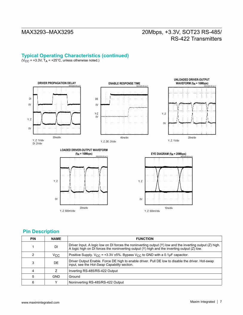
PIN NAME FUNCTION
1 DI Driver Input. A logic low on DI forces the noninverting output (Y) low and the inverting output (Z) high. A logic high on DI forces the noninverting output (Y) high and the inverting output (Z) low.
2 VCC Positive Supply. VCC = +3.3V ±5%. Bypass VCC to GND with a 0.1µF capacitor.
3 DE Driver Output Enable. Force DE high to enable driver. Pull DE low to disable the driver. Hot-swap input, see the Hot-Swap Capability section.
4 Z Inverting RS-485/RS-422 Output
5 GND Ground
6 Y Noninverting RS-485/RS-422 Output
EYE DIAGRAM (fIN = 20Mbps)MAX3293-95 toc14
10ns/divY, Z: 500mV/div
0V
Y, Z
LOADED DRIVER-OUTPUT WAVEFORM(fIN = 16Mbps)
MAX3293-95 toc13
20ns/divY, Z: 500mV/div
0V
Y, Z
UNLOADED DRIVER-OUTPUT WAVEFORM (fIN = 16Mbps)
MAX3293-95 toc12
20ns/divY, Z: 1V/div
0V
Y, Z
ENABLE RESPONSE TIMEMAX3293-95 toc11
40ns/div
DE
0V
0VY-Z
Y, Z, DE: 2V/div
DRIVER PROPAGATION DELAYMAX3293-95 toc10
20ns/divY, Z: 1V/divDI: 2V/div
DI
0V
0V
Y, Z
MAX3293–MAX3295 20Mbps, +3.3V, SOT23 RS-485/RS-422 Transmitters
Maxim Integrated 7www.maximintegrated.com
Pin Description
Typical Operating Characteristics (continued)

Detailed DescriptionThe MAX3293/MAX3294/MAX3295 are low-power trans-mitters for RS-485/RS-422 communication. The MAX3295 operates at data rates up to 20Mbps, the MAX3294 up to 2.5Mbps (slew-rate limited), and the MAX3293 up to 250kbps (slew-rate limited). These devices are enabled using an active-high driver enable (DE) input. When disabled, outputs enter a high-impedance state, and the supply current reduces to 1µA.The MAX3293/MAX3294/MAX3295 have a hot-swap input structure that prevents disturbance on the differential signal lines when a circuit board is plugged into a “hot” back-plane (see the Hot-Swap Capability section). Drivers are also short-circuit current limited and are protected against excessive power dissipation by thermal-shutdown circuitry.
DriverThe driver accepts a single-ended, logic-level input (DI) and translates it to a differential RS-485/RS-422 level output (Y and Z). Driving DE high enables the driver, while pulling DE low places the driver outputs (Y and Z) into a high-impedance state (see Table 1).
Low-Power ShutdownForce DE low to disable the MAX3293/MAX3294/ MAX3295. In shutdown mode, the device consumes a maximum of 10µA of supply current.
Hot-Swap CapabilityHot-Swap InputWhen circuit boards are inserted into a “hot” or pow-ered backplane, disturbances to the enable can lead to data errors. Upon initial circuit board insertion, the processor undergoes its power-up sequence. During this period, the output drivers are high impedance and are unable to drive the DE input of the MAX3293/ MAX3294/MAX3295 to a defined logic level. Leakage currents up to 10µA from the high-impedance out-put could cause DE to drift to an incorrect logic state. Additionally, parasitic circuit board capacitance could
cause coupling of VCC or GND to DE. These factors could improperly enable the driver.The MAX3293/MAX3294/MAX3295 eliminate all above issues with hot-swap circuitry. When VCC rises, an inter-nal pulldown circuit holds DE low for approximately 10µs. After the initial power-up sequence, the pulldown circuit becomes transparent, resetting the hot-swap tolerable input.
Figure 7. Differential Power-Up Glitch (0.1V/µs)
Figure 6. Simplified Structure of the Driver Enable Input (DE)
X = Don’t care.
Table 1. MAX3293/MAX3294/ MAX3295 (RS-485/RS-422) Transmitting Function Table
INPUTS OUTPUTSDE DI Y Z0 X Shutdown Shutdown1 0 0 11 1 1 0
DIFFERENTIAL POWER-UP GLITCH(0.1V/µs)
4µs/div
2V/divVCC
Y
Z
Y-Z
0V
10mV/divAC-COUPLED
10mV/divAC-COUPLED
20mV/div
VCC
TIMER
TIMER
ENDE
(HOT SWAP)
10µs
100µA
M1 M2
5.6kΩ
2mA
MAX3293–MAX3295 20Mbps, +3.3V, SOT23 RS-485/RS-422 Transmitters
www.maximintegrated.com Maxim Integrated 8

Hot-Swap Input CircuitryThe MAX3293/MAX3294/MAX3295 enable input fea-tures hot-swap capability. At the input, there are two NMOS devices, M1 and M2 (Figure 6). When VCC ramps from zero, an internal 10µs timer turns on M2 and sets the SR latch, which also turns on M1. Transistors M2, a 2mA current sink, and M1, a 100µA current sink, pull DE to GND through a 5.6kΩ resistor. M2 is designed to pull DE to the disabled state against an external parasitic capacitance up to 100pF that may drive DE high. After 10µs, the timer deactivates M2 while M1 remains on, holding DE low against three-state leakages that can drive DE high. M1 remains on until an external source overcomes the required input current. At this time, the SR latch resets and M1 turns
off. When M1 turns off, DE reverts to a standard, high-impedance CMOS input. Whenever VCC drops below 1V, the hot-swap input is reset.
Hot-Swap Line TransientDuring a hot-swap event when the driver is connected to the line and is powered up, the driver must not cause the differential signal to drop below 200mV. Figures 7, 8, and 9 show the results of the MAX3295 during power-up for three different VCC ramp rates (0.1V/µs, 1V/µs, and 10V/µs). The photos show the VCC ramp, the single-ended signal on each side of the 100Ω termination, as well as the differential signal across the termination.
ESD ProtectionHuman Body ModelFigure 10 shows the Human Body Model, and Figure 11 shows the current waveform it generates when discharged into low impedance. This model consists of a 100pF capac-itor charged to the ESD voltage of interest, which is then discharged into the device through a 1.5kΩ resistor.
Figure 11. Current Waveform
Figure 10. Human Body ESD Test
Figure 9. Differential Power-Up Glitch (10V/µs)
Figure 8. Differential Power-Up Glitch (1V/µs)
IP 100%90%
36.8%
tRL
TIME
tDLCURRENT WAVEFORM
PEAK-TO-PEAK RINGING(NOT DRAWN TO SCALE)
Ir
10%0V
0V
AMPERES
CHARGE-CURRENT-LIMIT RESISTOR
DISCHARGERESISTANCE
STORAGECAPACITOR
Cs100pF
RC 1MΩ
RD 1.5kΩ
HIGH-VOLTAGE
DCSOURCE
DEVICEUNDERTEST
DIFFERENTIAL POWER-UP GLITCH(10V/µs)
200ns/div
2V/divVCC
Y
Z
Y-Z
0V
50mV/divAC-COUPLED50mV/divAC-COUPLED
100mV/div
DIFFERENTIAL POWER-UP GLITCH(1V/µs)
1µs/div
2V/divVCC
Y
Z
Y-Z
0V100mV/divAC-COUPLED
100mV/divAC-COUPLED
200mV/div
MAX3293–MAX3295 20Mbps, +3.3V, SOT23 RS-485/RS-422 Transmitters
www.maximintegrated.com Maxim Integrated 9

Reduced EMI and Reflections (MAX3293/MAX3294)The MAX3293/MAX3294 are slew-rate limited, minimizing EMI and reducing reflections caused by improperly ter-minated cables. Figure 12 shows Fourier analysis of the MAX3295 transmitting a 125kHz signal. High-frequency harmonics with large amplitudes are evident. Figure 13 shows the same information, but for the slew-rate-limited MAX3293, transmitting the same signal. The high-fre-quency harmonics have much lower amplitudes, and the potential for EMI is significantly reduced.To minimize reflections, the line should be terminated at both ends in its characteristic impedance, and stub lengths off the main line should be kept as short as possible. The slew-rate-limited MAX3293 and MAX3294 are more toler-ant of imperfect termination.
Driver-Output ProtectionTwo mechanisms prevent excessive output current and power dissipation caused by faults or by bus contention. The first, a foldback current limit on the output stage, provides immediate protection against short circuits over the whole common-mode voltage range (see the Typical Operating Characteristics). The second, a thermal-shut-down circuit, forces the driver outputs into a high-imped-ance state if the die temperature exceeds +160°C.
Figure 13. Driver-Output Waveform and FFT Plot of MAX3293 Transmitting a 125kHz Signal
Figure 12. Driver-Output Waveform and FFT Plot of MAX3295 Transmitting a 125kHz Signal
PACKAGE TYPE
PACKAGE CODE
OUTLINE NO.
LANDPATTERN NO.
6 SOT23 U6CN+2 21-0058 90-0175
VCC
ZDE
1 6 Y+
5 GND
DI
MAX3293MAX3294MAX3295
SOT23-6
TOP VIEW
2
3 4
DRIVER-OUTPUT WAVEFORM AND FFT PLOT OF MAX3293
10dB/div
DRIVER-OUTPUT WAVEFORM ANDFFT PLOT OF MAX3295
10dB/div
MAX3293–MAX3295 20Mbps, +3.3V, SOT23 RS-485/RS-422 Transmitters
www.maximintegrated.com Maxim Integrated 10
Package InformationFor the latest package outline information and land patterns (footprints), go to www.maximintegrated.com/packages. Note that a “+”, “#”, or “-” in the package code indicates RoHS status only. Package drawings may show a different suffix character, but the drawing pertains to the package regardless of RoHS status.
Chip InformationPROCESS: BiCMOS
Pin Configuration

REVISION NUMBER
REVISION DATE DESCRIPTION PAGES
CHANGED
3 3/11 Added lead-free parts to the Ordering Information and Selector Guide tables 1
4 12/14 Added MAX3295AUT/V+T to Ordering Information 1
Maxim Integrated cannot assume responsibility for use of any circuitry other than circuitry entirely embodied in a Maxim Integrated product. No circuit patent licenses are implied. Maxim Integrated reserves the right to change the circuitry and specifications without notice at any time. The parametric values (min and max limits) shown in the Electrical Characteristics table are guaranteed. Other parametric values quoted in this data sheet are provided for guidance.
Maxim Integrated and the Maxim Integrated logo are trademarks of Maxim Integrated Products, Inc.
MAX3293–MAX3295 20Mbps, +3.3V, SOT23 RS-485/RS-422 Transmitters
© 2014 Maxim Integrated Products, Inc. 11
Revision History
For pricing, delivery, and ordering information, please contact Maxim Direct at 1-888-629-4642, or visit Maxim Integrated’s website at www.maximintegrated.com.