Embed Size (px)
Citation preview
General DescriptionThe MAX21105 is a monolithic 3-axis gyroscopes plus 3-axis accelerometer inertial measurement units (IMU) that provide unprecedented accuracy and stability over temperature and time.The MAX21105 is the industry’s most accurate 6 DoF inertial measurement units capable of working with a supply voltage as low as 1.71V designed to serve appli-cations such as drone/helicopter toys, handsets and tab-lets, game controllers, motion remote controls, and other consumer devices.In particular, the MAX21105 features low gyroscope zero-rate level error (GZRLE), low and linear gyroscope zero-rate level drift over temperature (GZRLDT) and low gyroscope phase delay (GPD) that makes the MAX21105 ideally suited for both flight and camera platforms stabili-zation on drone applications.A large 512-byte FIFO extends the time during which the application processor can stay in a power-saving state.The MAX21105 is available in a 3mm x 3mm x 0.83mm package 16-lead plastic land grid array (LGA) package and can operate within a temperature range of -40°C to +85°C.
Benefits and Features Accurate and Stable Performance Over Temperature
for Platform Stabilization• Low and Linear Zero-Rate Level Error Drift Over
Temperature (0.025dps/°C typ)• Low Bias Instability (4°/hour)• 16-Bit Output Temperature Sensor
Low-Power Operation Extends Battery Life• 3.8mA Low-Noise Mode Gyroscope + Accelerometer
Current Consumption• 2.2mA Low-Power Mode Gyroscope + Low-Noise
Mode Accelerometer Current Consumption• Power-Down Mode Current 1.5µA
Compact Package Reduces Board Space and Enhances Device Reliability• 3mm x 3mm x 0.83mm 16L LGA• High Shock Survivability (10,000 g Shock Tolerant)• -40°C to +85°C Extended Operating Temperature
Applications Platform Stabilization Motion Control with HMI (Human-Machine Interface) Motion-Enabled Portable Gaming GPS Navigation Inertial Navigation Systems Handsets and Tablets
Ordering Information appears and Recommended Application Schematics continued at end of data sheet.
19-7458; Rev 0; 12/14
MAINAPPLICATIONPROCESSOR
MAX21105
1
2
3
4
5
6 7 8
13
12
11
10
9
16 15 14REGD
RSV1
N.C.
V DD
SCL
SDA
INT1
INT2
SA0
N.C.
INT1
RSV0
INT2
CS
SA0_
SDO
SDA_
SDI_O
GND
SCL_CLK
N.C.
N.C.
VDDIO +
VDDIO
C1
VDD
C2
I2C MODE
C1
VDDIO
RPU RPUVDDIO
Recommended Application Schematics
MAX21105 Low-Power, Ultra-Accurate 6 DoF IMU
EVALUATION KIT AVAILABLE
A ADC
GYROSENSE
DSP
MAX21105
REGISTERSANDFIFO
GYRODRIVE
CONTROL
A+GMEMS
ACCELEROSENSE
DSP
ACCELERORAW DATA
GYRORAW DATA
DAC
VDDIO
BIAS AND LDOs
ADCA
A
A ADC
SPI/I2CSLAVE
RSV0
SCL_CLKSDA_SDI_O
SA0_SDO
CS
RSV1
TEMPERATURE SENSOROTP
CLOCKING
INTERRUPTSINT2
INT1
REGD GNDVDD
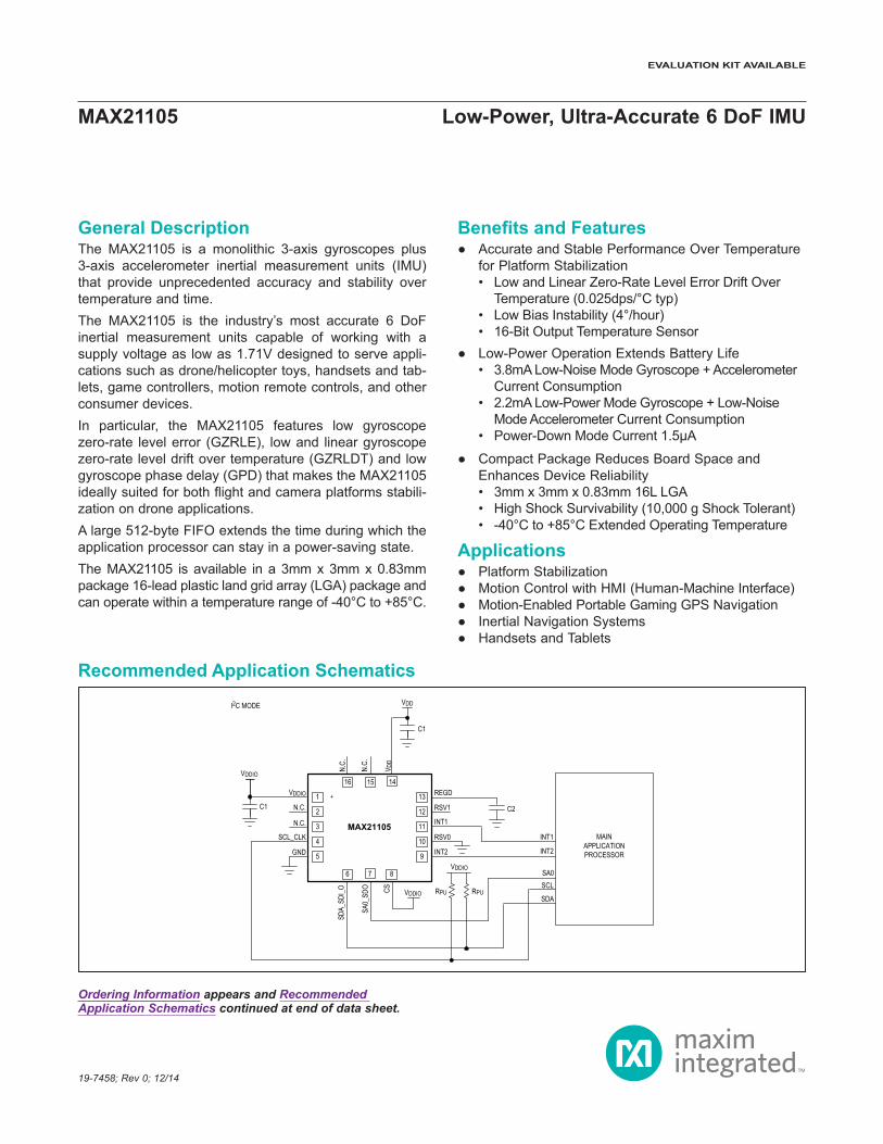
Functional Diagram
MAX21105 Low-Power, Ultra-Accurate 6 DoF IMU
www.maximintegrated.com Maxim Integrated 2
VDD .......................................................................-0.3V to +6.0VVDDIO ...................................................................-0.3V to +6.0VREGD ...................................... -0.3V to min (VDD + 0.3V,+2.2V)INT1, INT2, SDA_SDI_O, SA0_SDO, SCL_CLK,
CS, RSV0, RSV1 ...............-0.3V to min (VDDIO + 0.3V, 6.0V)
Operating Temperature Range ........................... -40°C to +85°CJunction Temperature ......................................................+150°CStorage Temperature Range ............................ -40°C to +150°CLead Temperature (soldering, 10s) .................................+260°C
LGA Junction-to-Case Thermal Resistance (θJC) ............31.8°C/W
Junction-to-Ambient Thermal Resistance (θJA) ........160°C/W
(Note 1)
(VDD = VDDIO = 1.8V, TA = -40°C to +85°C, unless otherwise noted. Typical values are at TA = +25°C.) (Note 2)
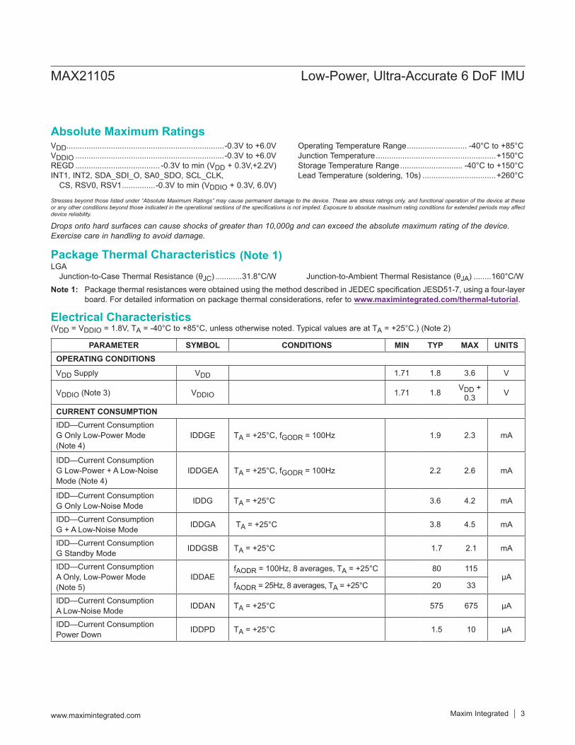
PARAMETER SYMBOL CONDITIONS MIN TYP MAX UNITSOPERATING CONDITIONS
VDD Supply VDD 1.71 1.8 3.6 V
VDDIO (Note 3) VDDIO 1.71 1.8 VDD + 0.3 V
CURRENT CONSUMPTIONIDD—Current ConsumptionG Only Low-Power Mode (Note 4)
IDDGE TA = +25°C, fGODR = 100Hz 1.9 2.3 mA
IDD—Current ConsumptionG Low-Power + A Low-Noise Mode (Note 4)
IDDGEA TA = +25°C, fGODR = 100Hz 2.2 2.6 mA
IDD—Current ConsumptionG Only Low-Noise Mode IDDG TA = +25°C 3.6 4.2 mA
IDD—Current ConsumptionG + A Low-Noise Mode IDDGA TA = +25°C 3.8 4.5 mA
IDD—Current ConsumptionG Standby Mode IDDGSB TA = +25°C 1.7 2.1 mA
IDD—Current ConsumptionA Only, Low-Power Mode (Note 5)
IDDAEfAODR = 100Hz, 8 averages, TA = +25°C 80 115
µAfAODR = 25Hz, 8 averages, TA = +25°C 20 33
IDD—Current ConsumptionA Low-Noise Mode IDDAN TA = +25°C 575 675 µA
IDD—Current ConsumptionPower Down IDDPD TA = +25°C 1.5 10 µA
Note 1: Package thermal resistances were obtained using the method described in JEDEC specification JESD51-7, using a four-layer board. For detailed information on package thermal considerations, refer to www.maximintegrated.com/thermal-tutorial.
Drops onto hard surfaces can cause shocks of greater than 10,000g and can exceed the absolute maximum rating of the device. Exercise care in handling to avoid damage.
Absolute Maximum Ratings
Stresses beyond those listed under “Absolute Maximum Ratings” may cause permanent damage to the device. These are stress ratings only, and functional operation of the device at these or any other conditions beyond those indicated in the operational sections of the specifications is not implied. Exposure to absolute maximum rating conditions for extended periods may affect device reliability.
Package Thermal Characteristics
Electrical Characteristics
MAX21105 Low-Power, Ultra-Accurate 6 DoF IMU
www.maximintegrated.com Maxim Integrated 3
(VDD = VDDIO = 1.8V, TA = -40°C to +85°C, unless otherwise noted. Typical values are at TA = +25°C.) (Note 2)
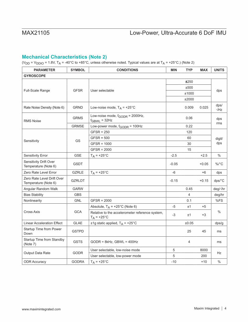
PARAMETER SYMBOL CONDITIONS MIN TYP MAX UNITSGYROSCOPE
Full-Scale Range GFSR User selectable
±250
dps±500
±1000
±2000
Rate Noise Density (Note 6) GRND Low-noise mode, TA = +25°C 0.009 0.025 dps/ √Hz
RMS NoiseGRMS Low-noise mode, fGODR = 2000Hz,
fGBWL = 32Hz 0.06 dps rms
GRMSE Low-power mode, fGODR = 100Hz 0.22
Sensitivity GS
GFSR = 250 120
digit/ dps
GFSR = 500 60
GFSR = 1000 30
GFSR = 2000 15
Sensitivity Error GSE TA = +25°C -2.5 +2.5 %
Sensitivity Drift Over Temperature (Note 6) GSDT -0.05 +0.05 %/°C
Zero Rate Level Error GZRLE TA = +25°C -6 +6 dps
Zero Rate Level Drift Over Temperature (Note 6) GZRLDT -0.15 +0.15 dps/°C
Angular Random Walk GARW 0.45 deg/√hr
Bias Stability GBS 4 deg/hr
Nonlinearity GNL GFSR = 2000 0.1 %FS
Cross Axis GCAAbsolute, TA = +25°C (Note 6) -5 ±1 +5
%Relative to the accelerometer reference system, TA = +25°C -3 ±1 +3
Linear Acceleration Effect GLAE ±1g static applied, TA = +25°C ±0.05 dps/g
Startup Time from Power Down GSTPD 25 45 ms
Startup Time from Standby (Note 7) GSTS GODR = 8kHz, GBWL = 400Hz 4 ms
Output Data Rate GODRUser selectable, low-noise mode 5 8000
HzUser selectable, low-power mode 5 200
ODR Accuracy GODRA TA = +25°C -10 +10 %
Mechanical Characteristics (Note 2)
MAX21105 Low-Power, Ultra-Accurate 6 DoF IMU
www.maximintegrated.com Maxim Integrated 4
(VDD = VDDIO = 1.8V, TA = -40°C to +85°C, unless otherwise noted. Typical values are at TA = +25°C.) (Note 2)
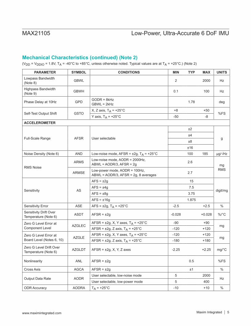
PARAMETER SYMBOL CONDITIONS MIN TYP MAX UNITSLowpass Bandwidth (Note 8) GBWL 2 2000 Hz
Highpass Bandwidth (Note 9) GBWH 0.1 100 Hz
Phase Delay at 10Hz GPD GODR = 8kHzGBWL = 2kHz 1.78 deg
Self-Test Output Shift GSTOX, Z axis, TA = +25°C +8 +50
%FSY axis, TA = +25°C -50 -8
ACCELEROMETER
Full-Scale Range AFSR User selectable
±2
g±4
±8
±16
Noise Density (Note 6) AND Low-noise mode, AFSR = ±2g, TA = +25°C 100 185 µg/√Hz
RMS NoiseARMS Low-noise mode, AODR = 2000Hz,
ABWL = AODR/3, AFSR = 2g 2.6mg
RMSARMSE Low-power mode, AODR = 100Hz,
ABWL = AODR/3, AFSR = 2g, 8 averages 2.7
Sensitivity AS
AFS = ±2g 15
digit/mgAFS = ±4g 7.5
AFS = ±8g 3.75
AFS = ±16g 1.875
Sensitivity Error ASE AFS = ±2g, TA = +25°C -2.5 +2.5 %
Sensitivity Drift Over Temperature (Note 6) ASDT AFSR = ±2g -0.028 +0.028 %/°C
Zero G Level Error at Component Level AZGLEC
AFSR = ±2g, X, Y axes, TA = +25°C -90 +90mg
AFSR = ±2g, Z axis, TA = +25°C -120 +120
Zero G Level Error at Board Level (Notes 6, 10) AZGLE
AFSR = ±2g, X, Y axes, TA = +25°C -120 +120mg
AFSR = ±2g, Z axis, TA = +25°C -180 +180
Zero G Level Drift Over Temperature (Note 6) AZGLDT AFSR = ±2g, X, Y, Z axes -2.25 +2.25 mg/°C
Nonlinearity ANL AFSR = ±2g 0.5 %FS
Cross Axis AGCA AFSR = ±2g ±1 %
Output Data Rate AODRUser selectable, low-noise mode 5 2000
HzUser selectable, low-power mode 5 400
ODR Accuracy AODRA TA = +25°C -10 +10 %
Mechanical Characteristics (continued) (Note 2)
MAX21105 Low-Power, Ultra-Accurate 6 DoF IMU
www.maximintegrated.com Maxim Integrated 5

(VDD = VDDIO = 1.8V, TA = -40°C to +85°C, unless otherwise noted. Typical values are at TA = +25°C.) (Note 2)Mechanical Characteristics (continued) (Note 2)
PARAMETER SYMBOL CONDITIONS MIN TYP MAX UNITS
Lowpass Bandwidth (Note 8) ABWLLow-noise mode AODR/48 AODR/3
HzLow-power mode AODR/48 AODR/2
Highpass Bandwidth (Note 9) ABWH AODR/400 AODR/50 Hz
Self-Test Output Shift ASTO TA = +25°C ±80 ±800 mg
TEMPERATURE SENSOR
Sensitivity TSS8 bit 1 digit/°C
16 bit 256 digit/°C
Sensitivity Error TSSE ±2 %
Output at +25°C TSO8 bit 25
digit16 bit 6400
Bandwidth TSBW 4 Hz
PARAMETER SYMBOL CONDITIONS MIN TYP MAX UNITSESD PROTECTIONHuman Body Model HBM 2000 V
Charged Device Model CDM 500 V
IOs DC SPECIFICATIONS (Note 6)
Input Threshold Low VIL 0.3 x VDDIO V
Input Threshold High VIH 0.7 x VDDIO V
Hysteresis of Schmitt Trigger Input VHYS 0.05 x VDDIO V
Input Leakage Current ILK -1 +1 µA
I2C Internal Pullup Resistance (Note 11) RI2CPU 4.5 10 kΩ
SPI SLAVE TIMING VALUES (Note 12)CLK Frequency fC_CLK 10 MHz
CS Setup Time tSU_CS 10 ns
CS Hold Time tH_CS 15 ns
SDI Input Setup Time tSU_SDI 10 ns
SDI Input Hold Time tH_SDI 15 ns
CLK Fall to SDO Valid Output Time tV_SDO 40 ns
SDO Output Hold Time tH_SDO 5 ns
Interface Specifications (Note 2)
MAX21105 Low-Power, Ultra-Accurate 6 DoF IMU
www.maximintegrated.com Maxim Integrated 6
Note 2: Limits are 100% tested at TA = +25°C. Limits over the operating temperature range and relevant supply voltage range are guaranteed by design and characterization.
Note 3: VDDIO must be lower or equal than VDD supply for normal operation. With VDDIO supplied and VDD not supplied, the I/O pads are in high impedance.
PARAMETER SYMBOL CONDITIONS MIN TYP MAX UNITS
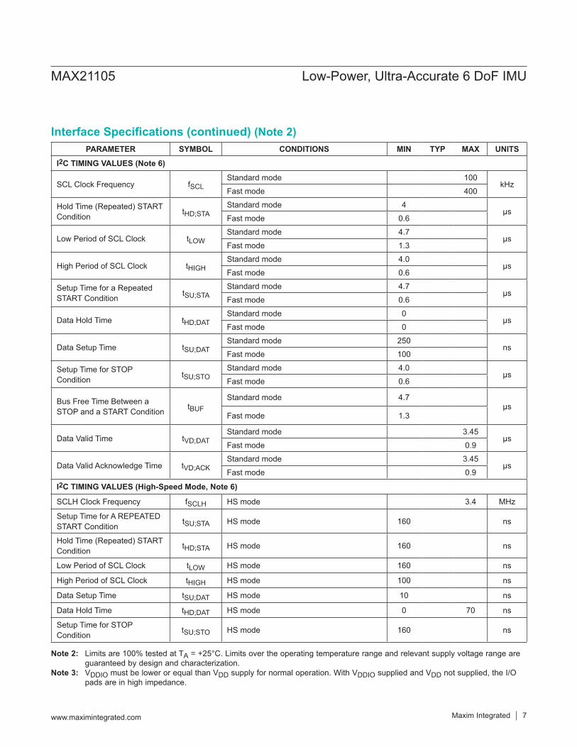
I2C TIMING VALUES (Note 6)
SCL Clock Frequency fSCLStandard mode 100
kHzFast mode 400
Hold Time (Repeated) START Condition tHD;STA
Standard mode 4µs
Fast mode 0.6
Low Period of SCL Clock tLOWStandard mode 4.7
µsFast mode 1.3
High Period of SCL Clock tHIGHStandard mode 4.0
µsFast mode 0.6
Setup Time for a Repeated START Condition tSU;STA
Standard mode 4.7µs
Fast mode 0.6
Data Hold Time tHD;DATStandard mode 0
µsFast mode 0
Data Setup Time tSU;DATStandard mode 250
nsFast mode 100
Setup Time for STOP Condition tSU;STO
Standard mode 4.0µs
Fast mode 0.6
Bus Free Time Between a STOP and a START Condition tBUF
Standard mode 4.7µs
Fast mode 1.3
Data Valid Time tVD;DATStandard mode 3.45
µsFast mode 0.9
Data Valid Acknowledge Time tVD;ACKStandard mode 3.45
µsFast mode 0.9
I2C TIMING VALUES (High-Speed Mode, Note 6)
SCLH Clock Frequency fSCLH HS mode 3.4 MHz
Setup Time for A REPEATED START Condition tSU;STA HS mode 160 ns
Hold Time (Repeated) START Condition tHD;STA HS mode 160 ns
Low Period of SCL Clock tLOW HS mode 160 ns
High Period of SCL Clock tHIGH HS mode 100 ns
Data Setup Time tSU;DAT HS mode 10 ns
Data Hold Time tHD;DAT HS mode 0 70 ns
Setup Time for STOP Condition tSU;STO HS mode 160 ns
Interface Specifications (continued) (Note 2)
MAX21105 Low-Power, Ultra-Accurate 6 DoF IMU
www.maximintegrated.com Maxim Integrated 7
Note 4: In low-power mode, the gyroscope has higher rate noise density, but lower current consumption. In this condition, the gyro selectable output data rate (ODR) ranges from 5Hz to 200Hz.
Note 5: In low-power mode, the accelerometer has higher noise density, but lower current consumption. In this condition, the selectable output data rate (ODR) of the accelerometer ranges from 5Hz to 400Hz.
Note 6: Guaranteed by design, not production tested.Note 7: In standby, only the gyro drive circuit is powered on, and in this condition, the outputs are not available. In this condition,
the startup time depends only on the filters responses.Note 8: User selectable.Note 9: Enable/disable with user-selectable bandwidth.Note 10: Values after MSL3 preconditioning and 3 reflow cycles.Note 11: Pullup resistances are user selectable.Note 12: 10pF load on SPI lines. Min Max based on characterization results.
tH_SO
CS
CLK
SDI
SDO
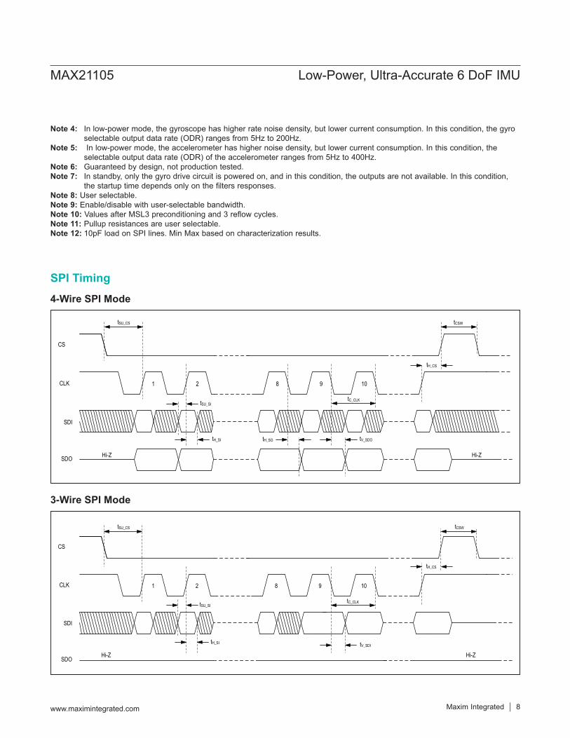
tSU_CS tCSW
tH_CS
1 2 8 9 10
tSU_SItC_CLK
Hi-Z
tH_SI tV_SDO
Hi-Z
CS
CLK
SDI
SDO
1
tSU_CS
tSU_SI
tH_SI
tH_CS
2
tCSW
8 9 10
tC_CLK
Hi-ZtV_SDI
Hi-Z
SPI Timing
4-Wire SPI Mode
3-Wire SPI Mode
MAX21105 Low-Power, Ultra-Accurate 6 DoF IMU
www.maximintegrated.com Maxim Integrated 8

tSU;DAT
tVD;DATtHD;DAT
tHD;STAtSU;STA
VIL = 0.3VDDVIH = 0.7VDD
tLOW
tBUF
tSU;STOtVD;ACK
9th CLOCK
9th CLOCK 002aac938
1/fSCL1st CLOCK CYCLE
tHIGH
70%30%
70%30%
70%30%
70%30%
70%30%
70%
70%
S
Sr SP
SCL
SCL
SDA
SDA
30%
30% cont.
cont.
tF tR
tR
tHD;STA
tF
= MCS CURRENT SOURCE PULLUP
SCLH
SDAH
= RP RESISTOR PULLUP
tLOWtLOW
trCLtrCL1
Sr P
tfCL
tSU;DAT
tSU;STOtHD;DAT
tHD;STAtSU;STA
tfDA trDASr
trCL1tHIGHtHIGH
(1)(1)
(1) FIRST RISING EDGE OF THE SCLH SIGNAL AFTER Sr AND AFTER EACH ACKNOWLEDGE BIT.
I2C HIGH-SPEED DIAGRAM
I2C Timing
Standard/Fast Mode I2C Bus Timing
High-Speed Mode I2C Bus Timing
MAX21105 Low-Power, Ultra-Accurate 6 DoF IMU
www.maximintegrated.com Maxim Integrated 9
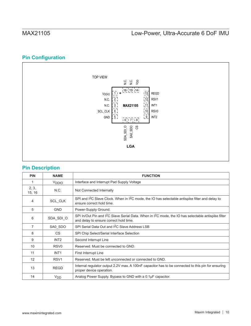
PIN NAME FUNCTION
1 VDDIO Interface and Interrupt Pad Supply Voltage
2, 3, 15, 16 N.C. Not Connected Internally
4 SCL_CLK SPI and I2C Slave Clock. When in I2C mode, the IO has selectable antispike filter and delay to ensure correct hold time.
5 GND Power-Supply Ground.
6 SDA_SDI_O SPI In/Out Pin and I2C Slave Serial Data. When in I2C mode, the IO has selectable antispike filter and delay to ensure correct hold time.
7 SA0_SDO SPI Serial Data Out and I2C Slave Address LSB
8 CS SPI Chip Select/Serial Interface Selection
9 INT2 Second Interrupt Line
10 RSV0 Reserved. Must be connected to GND.
11 INT1 First Interrupt Line
12 RSV1 Reserved. Must be left unconnected or connected to GND.
13 REGD Internal regulator output 2.2V max. A 100nF capacitor has to be connected to this pin for ensuring proper device operation.
14 VDD Analog Power Supply. Bypass to GND with a 0.1µF capacitor.
TOP VIEW
MAX21105
LGA
INT2
RSV0
INT1
RSV1
REGD
GND
SCL_CLK
N.C.
N.C.VDDIO
5
4
3
2
1
9
10
11
12
1315 1416
876
CS
SDA_
SDI_O
V DD
N.C.
N.C.
SA0_
SDO
+
Pin Description
Pin Configuration
MAX21105 Low-Power, Ultra-Accurate 6 DoF IMU
www.maximintegrated.com Maxim Integrated 10

Detailed DescriptionThe MAX21105 is a low-power, low voltage, small pack-age 6-axis inertial measurement unit that provides unprecedented accuracy and stability over temperature and time.The MAX21105 integrates a 3-axis gyroscope and 3-axis linear accelerometer in a 3mm x 3mm x 0.83mm package capable of working with a supply voltage as low as 1.71V.They include a sensing element and an IC interface capable of providing the measured angular rate and acceleration to the external world through a digital inter-face (I2C/SPI).The MAX21105 sensor data can be stored into a 512- byte, fully configurable, embedded FIFO.The MAX21105 features a wide selection of dynamically selectable power modes that allow the user to optimize the system power consumption based on the application needs.The MAX21105 has a full scale of ±250/±500/±1000/±2000 dps for gyroscope and ±2/±4/±8/±16g for accelerometer. It is capable of measuring angular rates and accelerations with a user-selectable bandwidth.The MAX21105 is available in a 3mm x 3mm x 0.83mm 16-lead plastic land grid array (LGA) package and oper-ate over the -40°C to +85°C temperature range.
DefinitionsPower supply [V]: This parameter defines the operat-ing DC power-supply voltage range of the 6DoF inertial measurement unit. Although it is always a good practice to keep VDD clean with minimum ripple, unlike most of the competitors, who require an ultra-low noise, low-dropout regulator to power the device, the MAX21105 can operate at 1.71V, but that supply can also be provided by a switch-ing regulator to minimize the system power consumption.Current consumption in low-noise mode [mA]: This parameter defines the typical current consumption when the 6DoF inertial measurement unit is operating with the lowest noise for both the accelerometer and gyroscope.Current consumption in low-power mode [mA]: This parameter defines the current consumption when the 6DoF inertial measurement unit is in low-power mode. Whilst in low-power mode, the MAX21105 significantly reduces power consumption, but increase noise.Current consumption in power-down mode [µA]: This parameter defines the current consumption when the
6DoF inertial measurement unit is powered down. In this mode, both the mechanical sensing structure and read-ing chain are turned off. Users can configure the control register through the I2C/SPI interface for this mode. Full access to the control registers through the I2C/SPI inter-faces is also guaranteed in power-down mode.Gyroscope full-scale range [dps]: This parameter defines the measurement range of the gyroscope in degrees per second (dps). When the applied angular rate is beyond the full-scale range, the gyroscope output becomes saturated.Zero-rate level [dps]: This parameter defines the DC device output when there is no external angular rate applied to the gyroscope.Gyroscope sensitivity [digit/dps]: Sensitivity is the relationship between 1 LSb and dps. It can be used to convert a digital gyroscope’s measurement from digits to angular rate.Zero-rate level change vs. temperature [dps/°C]: This parameter defines the zero-rate level change in dps/°C over the operating temperature range.Gyroscope sensitivity change vs. temperature [%/°C]: This parameter defines the gyroscope sensitivity change as a percentage (%) over the operating temperature range specified in the data sheet.Gyroscope nonlinearity [% FS]: This parameter defines the maximum absolute difference between the gyroscope output and the best-fit straight line as a percentage of the gyroscope full-scale (GFS) range.Gyroscope bandwidth [Hz]: This parameter defines the frequency of the angular rate signal from DC to the built-in bandwidth (GBWL) that the gyroscope can measure. A dedicated register can be used to select the gyroscope bandwidth.Rate noise density [dps/√Hz]: This parameter defines the square root of the equivalent noise power density of the gyroscope angular rate.Accelerometer full-scale range [g]: This parameter defines the measurement range of the accelerometer in g. When the applied acceleration is beyond the full-scale range, the accelerometer output becomes saturated.Zero-g level [mg]: This parameter defines the DC device output when there is no external acceleration applied to the accelerometer.
MAX21105 Low-Power, Ultra-Accurate 6 DoF IMU
www.maximintegrated.com Maxim Integrated 11

Accelerometer sensitivity [digit/g]: Sensitivity is the relationship between LSb and g. It can be used to convert a digital acceleration measurement from digits to g.Zero-g level change vs. Temperature [mg/°C]: This parameter defines the zero-g level change in mg/°C over the operating temperature range.Accelerometer Sensitivity change vs. temperature [%/°C]: This parameter defines the accelerometer sen-sitivity change as a percentage (%) over the operating temperature range specified in the data sheet.Accelerometer nonlinearity [% FS]: This parameter defines the maximum absolute difference between the accelerometer output and the best-fit straight line as a percentage of the full-scale (FS) range.Accelerometer bandwidth [Hz]: This parameter defines the frequency of the acceleration signal from DC to the built-in bandwidth (ABWL) that the accelerometer can measure. A dedicated register can be used to select the accelerometer bandwidth.Accelerometer noise density [µg/√Hz]: This parameter defines the square root of the equivalent noise power density of accelerometer linear acceleration.
MAX21105 ArchitectureThe MAX21105 comprises the following key blocks and functions:
3-axis MEMS gyroscope sensor with 16-bit ADCs and signal conditioning
3-axis MEMS accelerometer sensor with 16-bit ADCs and signal conditioning
Slave I2C and SPI serial communications interfaces
Interrupt generators Digital output temperature sensor Power management enabling different power modes Sensor data registers FIFO Self-test functionality
Three-Axis MEMS Gyroscope with 16-Bit ADCs and Signal ConditioningThe MAX21105 includes a MEMS gyroscope that detects angular rates around the X, Y, and Z axes through the related IC interface. When the gyroscope rotates around
any of the sensing axes, the Coriolis Force determines a displacement in the MEMS structure, which is detected as a capacitive variation. The resulting signal is then processed by the 16-bit ADC to produce a digital output proportional to the angular rate. The gyro full-scale range can be digitally programmed at ±250, ±500, ±1000 or ±2000 dps.
Three-Axis MEMS Accelerometer Sensor with 16-Bit ADCs and Signal ConditioningThe MAX21105 includes a MEMS accelerometer that detects linear accelerations along the X, Y, and Z axes. The acceleration applied to one of the sensing axes causes a displacement of the MEMS structure which is detected as a capacitive variation. The signal is then con-verted in the digital domain by 16-bit ADC and is available to the user as a digital output proportional to the applied acceleration. The accelerometer full-scale range can be digitally programmed at ±2, ±4, ±8 or ±16 g.
Slave I2C and SPI Serial Communications InterfacesThe registers embedded inside the MAX21105 can be accessed through both the slave I2C and SPI serial inter-faces. The latter can be SW configured to operate either in 3-wire or 4-wire interface mode.The serial interfaces are mapped onto the same pins. To select/exploit the I2C interface, CS line must be tied high (i.e., connected to VDDIO).
I2C InterfaceI2C is a two-wire interface comprised of the signals serial data (SDA) and serial clock (SCL). In general, the lines are open-drain and bidirectional. In a generalized I2C interface implementation, attached devices can be a master or a slave. The master device puts the slave address on the bus, and the slave device with the match-ing address acknowledges the master.The MAX21105 operates as a slave device when com-municating to the system processor, which thus acts as the master. SDA and SCL lines typically need pull-up resistors to VDDIO. The maximum bus speed is 3.4MHz (I2C HS); this reduces the amount of time the system processor is kept busy in supporting the exchange of data.The slave address of the MAX21105 is b101100X, which is 7 bits long. The LSb of the 7-bit address is determined by the logic level on pin SA0. This allows two MAX21105s to be connected on the same I2C bus.
MAX21105 Low-Power, Ultra-Accurate 6 DoF IMU
www.maximintegrated.com Maxim Integrated 12

When used in this configuration, the address of one of the two devices should be b1011000 (pin SA0_SD0 is set to logic low) and the address of the other should be b1011001 (pin SA0_SD0 is set to logic-high).
SPI InterfaceThe MAX21105 SPI can operate up to 10MHz, in both 3-wires (half duplex) and 4-wires mode (full duplex).It is recommended to set the I2C_OFF bit at address 0x16 if the MAX21105 is used together with other SPI devices to avoid the possibility to switch inadvertently into I2C mode when traffic is detected with the CS unasserted.The MAX21105 operates as an SPI slave device.Both the read register and write register commands are completed in 16 clock pulses, or in multiples of 8 in case of multiple read/write bytes. Bit duration is the time between two fall-ing edges of CLK.The first bit (bit 0) starts at the first falling edge of CLK after the falling edge of CS while the last bit (bit 15, bit 23, etc.) starts at the last falling edge of CLK just before the rising edge of CS.Bit 0: RW bit. When 0, the data DI(7:0) is written to the device. When 1, the data DO(7:0) from the device is read. In the latter case, the chip drives SDO at the start of bit 8.Bit 1: MS bit. Depending on the configuration of IF_PARITY this bit may either be used to operate in multi-addressing standard mode or to check the parity with the register address.
If used as a MS bit, when 1, the address remains unchanged in multiple read/write commands, whilst when 0, the address is autoincremented in multiple read/write commands.Bit 2–7: Address AD(5:0). This is the address field of the indexed register.Bit 8–15: Data DI(7:0) (write mode). This is the data that is written to the device (MSb first).Bit 8–15: Data DO(7:0) (read mode). This is the data that is read from the device (MSb first).
SPI Half- and Full-Duplex OperationThe MAX21105 can be programmed to operate in half-duplex (a bidirectional data pin) or full-duplex (one data-in and one data-out pin) mode. The SPI master sets a reg-ister bit called SPI_3_WIRE into I2C_CFG (0x16) to 0 for full-duplex, and 1 for half-duplex operation. Full duplex is the power-on default.
Full-Duplex OperationThe MAX21105 is put into full-duplex mode at power-up. When the SPI master clears the SPI_3_WIRE bit, the SPI interface uses separate data pins, SDI and SDO, to transfer data. Because of the separate data pins, bits can be simultaneously clocked into and out of the MAX21105. The MAX21105 makes use of this feature by clocking out 8 output data bits as the command byte is clocked in.
Table 1. Digital Interface Pin Description
Table 2. I2C Address
NAME DESCRIPTION
CS SPI enable and I2C/SPI mode selection (1: I2C mode, 0: SPI enabled)
SCL/CLK SPI and I2C clock. When in I2C mode, the IO has selectable anti-spike filter and delay to ensure correct hold time.
SDA/SDI/SDO SPI in/out pin and I2C serial data. When in I2C mode, the IO has selectable antispike filter and delay to ensure correct hold time.
SDO/SA0 SPI serial data out or I2C slave address LSb
I2C BASE ADDRESS SA0/SDO PIN R/W BIT RESULTING ADDRESS
0x2C (6 bit) 0 0 0xB0
0x2C 0 1 0xB1
0x2C 1 0 0xB2
0x2C 1 1 0xB3
MAX21105 Low-Power, Ultra-Accurate 6 DoF IMU
www.maximintegrated.com Maxim Integrated 13
Reading from the SPI Slave Interface (SDO)The SPI master reads data from the MAX21105 slave interface using the following steps:1) When CS is high, the MAX21105 is unselected and
three-states the SDO output.2) After driving SCL_CLK to its inactive state, the SPI
master selects the MAX21105 by driving CS low.3) The SPI master clocks the command byte into the
MAX21105. The SPI read command is performed with 16 clock pulses. Multiple byte read command is per-formed adding blocks of 8 clock pulses at the previous one.
Bit 0: READ bit. The value is 1. Bit 1: MS bit. When 1, do not increment address,
when 0, increment address in multiple reading. Bit 2–7: Address AD(5:0). This is the address field of
the indexed register. Bit 8–15: Data DO(7:0) (read mode). This is the data
that is read from the device (MSb first). Bit 16–... : Data DO(...-8). Further data in multiple byte
reading. After 16 clock cycles, the master can drive CS high to deselect the MAX21105, causing it to three- state its SDO output. The falling edge of the clock puts the MSB of the next data byte in the sequence on the SDO output.
4) By keeping CS low, the master clocks register data bytes out of the MAX21105 by continuing to supply SCL_CLK pulses (burst mode). The master terminates the transfer by driving CS high. The master must ensure that SCL_CLK is in its inactive state at the beginning of the next access (when it drives CS low).
Writing to the SPI Slave Interface (SDI)The SPI master writes data to the MAX21105 slave inter-face through the following steps:1) The SPI master sets the clock to its inactive state.
While CS is high, the master can drive the SDI input.2) The SPI master selects the MAX21105 by driving CS
low3) The SPI master clocks the command byte into the
MAX21105. The SPI write command is performed with 16 clock pulses. Multiple byte write command is performed adding blocks of 8 clock pulses at the previous one.
Bit 0: WRITE bit. The value is 0. Bit 1: MS bit. When 1, do not increment address,
when 0, increment address in multiple writing. Bit 2–7: address AD(5:0). This is the address field of
the indexed register. Bit 8–15: Data DI(7:0) (write mode). This is the data
that is written inside the device (MSb first). Bit 16–... : data DI(...-8). Further data in multiple byte
writing.4) By keeping CS low, the master clocks data bytes into
the MAX21105 by continuing to supply SCL_CLK pulses (burst mode). The master terminates the trans-fer by driving CS high. The master must ensure that SCL_CLK is inactive at the beginning of the next access (when it drives CS low).
Half-Duplex OperationWhen the SPI master sets SPI_3_WIRE = 1, the MAX21105 is put into half-duplex mode. In half-duplex mode, the MAX21105 three-states its SDO pin and makes the SDI pin bidirectional, saving a pin in the SPI interface. The SDO pin can be left unconnected in half-duplex operation. The SPI master accesses a MAX21105 regis-ter as follows: the SPI master sets the clock to its inactive state. While CS is high, the master can drive the SDI pin to any value.1) The SPI master selects the MAX21105 by driving CS
low and placing the first data bit (MSB) to write on the SDI input.
2) The SPI master turns on its output driver and clocks the command byte into the MAX21105. The SPI read command is performed with 16 clock pulses:
Bit 0: READ bit. The value is 1. Bit 1: MS bit. When 1, do not increment address,
when 0, increment address in multiple reading. Bit 2-7: address AD(5:0). This is the address field of
the indexed register. Bit 8-15: data DO(7:0) (read mode). This is the data
that is read from the device (MSb first). Multiple read command is also available in 3-wire
mode.
MAX21105 Low-Power, Ultra-Accurate 6 DoF IMU
www.maximintegrated.com Maxim Integrated 14
Interrupt GeneratorsThe MAX21105 offers two completely independent inter-rupt generators, to ease the SW management of the interrupt generated. For instance, one line could be used to signal a DATA_READY event whilst the other line might be used, for instance, to notify the completion of the inter-nal start-up sequence.Interrupt functionality can be configured through the Interrupt Configuration registers. Configurable items include the INT pin level and duration, the clearing meth-od as well as the required triggers for the interrupts.The interrupt status can be read from the Interrupt Status registers.The event that has generated an interrupt is available in both forms: latched and unlatched.Interrupt sources may be enabled/ disabled and cleared individually. The list of possible interrupt sources includes the following conditions: DATA_READY, FIFO_EMPTY, FIFO_THRESHOLD, FIFO_OVERRUN, OTP_DOWNLOAD.The interrupt generation can also be configured as latched, unlatched or timed, with programmable length.When configured as latched, the interrupt can be cleared by reading the corresponding status register (clear-on-read) or by writing an appropriate mask to the status register (clear-on-write).
Digital-Output Temperature SensorAn digital output temperature sensor is used to measure the MAX21105 die temperature. The readings from the ADC can be accessed from the Sensor Data registers.The temperature data is split over 2 bytes. For faster and less accurate reading, accessing the MSB allows to read the temperature data as an absolute value expressed in Celsius degrees. By reading the LSB, the accuracy is greatly increased, up to 256 digit/°C.
Power ModesThe MAX21105 features nine power modes, allowing selecting the appropriate tradeoff between power con-sumption, noise level, accuracy and turn-on time.The transition between different power modes can be con-trolled with the software by explicitly setting a power mode in the Configuration register.
Gyro Low-Noise ModeIn gyro low-noise mode, only the gyro is switched on and it is operational with minimum noise level.
Gyro Low-Power ModeIn this power mode, only the gyro is switched on and it is operating in low-power mode. The low-power mode allows to reduce power consumption with the same sen-sor accuracy at the price of a higher rate noise density.This unique MAX21105 features can be activated for the gyro with different ODR from 5Hz to 200Hz.
Gyro Standby ModeTo reduce power consumption and have a shorter turn-on time, the IC features a standby mode for the gyro. In standby mode, the MAX21105 gyro does not gen-erate data because a significant portion of the signal processing resources is turned off to save power. Still, this mode enables a much quicker turn-on time.
Acc Low-Noise ModeIn acc low-noise mode, only the accelerometer is switched on. It is operational with minimum noise level.
Acc Low-Power ModeIn this power mode, only the accelerometer is switched on, and it is operating in low-power mode. The low-power mode allows to reduce power consumption with the same sensor accuracy at the price of a higher accelerometer noise density.This feature can be activated for accelerometer with dif-ferent ODR from 5Hz to 400Hz.
Power-Down ModeIn Power-Down Mode, the IC is configured to minimize the power consumption. In Power-Down Mode, registers can still be read and written, but neither sensor can generate new data. Compared to Standby Mode, it takes longer to activate the IC and start collecting data from the sensors.
Sensor Data Output RegistersThe sensor data registers contain the latest gyroscope, accelerometer, and temperature measurement data.They are read-only registers and are accessed through the serial interface. Data from these registers can be read at anytime. However, the interrupt function can be used to determine when new data is available.
FIFOThe MAX21105 embeds a 512-byte data FIFO. The user can flexibly select the set of axis data to be stored in FIFO.This allows a power saving at system level as the host processor does not need to continuously poll data from the sensor, but it can wake up only when needed and burst the significant data out from the FIFO.
MAX21105 Low-Power, Ultra-Accurate 6 DoF IMU
www.maximintegrated.com Maxim Integrated 15
The FIFO buffer can work according to four main modes: off, normal, interrupt, and snapshot.When configured in snapshot mode, it offers the ideal mechanism to capture the data following an external inter-rupt event.Both normal and interrupt modes can be optionally configured to operate in overrun mode, depending on whether, in case of buffer underrun, newer or older data are accepted to be lost.Various FIFO status flags can be enabled to generate interrupt events on INT1/INT2 pin.
FIFO Off ModeIn this mode, the FIFO is turned off; data are stored only in the data registers and no data are available from the FIFO if read.When the FIFO is turned off, there are essentially two options to use the device: synchronous and asynchro-nous reading through the data registers.
Synchronous ReadingIn this mode, the processor reads the data set (e.g., 6 bytes for a 3 axes configuration) generated by the MAX21105 every time that DATA_READY is set. The processor must read once and only once the data set in order to avoid data inconsistencies.Benefits of using this approach include the perfect recon-struction of the signals coming the MAX21105 with the minimum data traffic.
Asynchronous ReadingIn this mode, the processor reads the data generated by the MAX21105, regardless the status of the DATA_READY flag. To minimize the error caused by different samples being read a different number of times, the access fre-quency to be used must be much higher than the selected ODR. This approach normally requires a much higher BW.
FIFO Normal ModeOverrun = false
FIFO is turned on. FIFO is filled with the data at the selected output
data rate (ODR). When FIFO is full, an interrupt can be generated. When FIFO is full, all the new incoming data is dis-
charged. Reading only a subset of the data already stored into the FIFO keeps locked the possibility for new data to be written.
Only if all the data are read, the FIFO restarts saving data. If communication speed is high, data loss can be
prevented. To prevent a FIFO-full condition, the required condi-
tion is to complete the reading of the data set before the next DATA_READY occurs.
If this condition is not guaranteed, data can be lost.
MAX21105 Low-Power, Ultra-Accurate 6 DoF IMU
www.maximintegrated.com Maxim Integrated 16
Overrun = true FIFO is turned on. FIFO is filled with the data at the selected ODR. When FIFO is full, an interrupt can be generated. When FIFO is full, the oldest data is overwritten with
the new ones. If communication speed is high, data integrity can be
preserved. In order to prevent a FIFO_WR_FULL condition, the
required condition is to complete the reading of the data set before the next DATA_READY occurs.
If this condition is not guaranteed, data can be overwritten.
Interrupt ModeOverrun = false
FIFO is initially disabled. Data are stored only in the data registers.
When an interrupt (either INT_OR or INT_AND) is generated, the FIFO is turned on automatically. It stores the data at the selected ODR.
When FIFO is full, all the new incoming data is dis-charged. Reading only a subset of the data already stored into the FIFO keeps locked the possibility for new data to be written.
Only if all the data are read the FIFO restarts saving data when a new event is generated.
Overrun = true FIFO is initially disabled. Data are stored only in the
data registers. When an interrupt (either INT_OR or INT_AND) is
generated, the FIFO is turned on automatically. It stores the data at the selected ODR.
When FIFO is full, an interrupt can be generated. When FIFO is full, the oldest data is overwritten with
the new ones. If communication speed is high, data integrity can be
preserved. In order to prevent a FIFO_WR_FULL condition, the
required condition is to complete the reading of the data set before the next DATA_READY occurs.
If this condition is not guaranteed, data can be over-written.
Snapshot Mode FIFO is initially in normal mode with overrun enabled. When an interrupt (either INT_OR or INT_AND) is
generated, the FIFO switches automatically to not-overrun mode, and data stops being saved in the FIFO, regardless whether the FIFO is full or not.
When FIFO is full, an interrupt can be generated. When FIFO is full, all the new incoming data is dis-
charged. Reading only a subset of the data already stored into the FIFO keeps locked the possibility for new data to be written.
Only if all the data are read the FIFO restarts saving data in overrun mode.
Table 3. Power ModesNAME DESCRIPTION
Gyro Low Noise Only gyroscope is switched on and it is operational with maximum performances.Gyro Low Power Only gyroscope is switched on and operates to reduce the average current consumption.
Gyro Standby The gyroscope is in standby mode, the current consumption is reduced by 50%, with a shorter turn-on time.
Acc Low Noise Only accelerometer is switched on and it is operational with maximum performances.Acc Low Power Only accelerometer is switched on and operates to reduce the average current consumption.Gyro Low-Noise Mode + Acc Low-Noise Mode Acc and gyro are both switched on in low-noise mode.
Gyro Low-Power + Acc Low-Noise Mode Acc is in low-noise mode, while the gyro is low-power mode.
Gyro Standby + Acc Low-Noise Mode Acc is in low-noise mode, while the gyro is standby mode.
Power-Down This is the minimum power consumption mode, at the price of a longer turn-on time.
MAX21105 Low-Power, Ultra-Accurate 6 DoF IMU
www.maximintegrated.com Maxim Integrated 17

Self-TestGyroscopeThis gyroscope embedded self-test feature can be used to verify if the gyroscope is working properly without physically rotating the device. That may be used either before or after it is assembled on a PCB. If the gyroscope’s
outputs are within the specified self-test values in the data sheet, then the gyroscope is working properly.
AccelerometerThe accelerometer embedded self-test feature is used to verify the sensor functionality without physically moving the device. When this feature is enabled, an electrostatic test force is applied to the mechanical sensing element
Figure 1. FIFO Normal mode, Overrun = False
Figure 2. FIFO Normal Mode, Overrun = True
MAX
THRESHOLD THRESHOLD THRESHOLD
MAX
LEVEL INCREMENTS WITH NEWSAMPLES STORED AND DECREMENTS
WITH NEW READINGS.
FIFO_TH INTERRUPTGENERATED.
FIFO_FULL INTERRUPT GENERATED.NO NEW DATA STORED UNTIL
THE ENTIRE FIFO IS READ.
(WP-RP)=
LEVEL
0
(WP-RP)=
LEVEL
(WP-RP)=
LEVEL
0
MAX
0
THRESHOLD
THRESHOLD THRESHOLD
FIFO USED ASCIRCULAR BUFFER
FIFO USED ASCIRCULAR BUFFER
FIFO USED ASCIRCULAR BUFFER
WP
RP
WP
RP
WPRP
WP-RP INCREMENTS WITH NEWSAMPLES STORED AND DECREMENTS
WITH NEW READINGS.
FIFO_TH INTERRUPTGENERATED.
FIFO_FULL INTERRUPT GENERATED.NEW INCOMING DATA WOULD
OVERWRITE THE OLDER ONES.
MAX21105 Low-Power, Ultra-Accurate 6 DoF IMU
www.maximintegrated.com Maxim Integrated 18

and causes the moving part to move away from its origi-nal position, emulating a definite input acceleration. In this case the sensor outputs exhibit a change in their DC levels which is related to the selected full scale through the device sensitivity. The output in this self-test mode is then compared with the output data of the device when the self-test is disabled. If the absolute value of the output difference is within the minimum and maximum range of the preselected full scale range, the accelerometer is working properly.
Revision IDThe MAX21105 has a register used to identify the revision ID of the device and to identify the specific part number. Even though different part numbers may share the same WHO_AM_I value, they would still be identified by means of different Revision ID values.
Unique Serial NumberEach MAX21105 device is uniquely identified by 48 bits that can be used to track the history of the sample, includ-ing manufacturing, assembly, and testing information.
Register FileThe register file is organized per banks. On the Common Bank are mapped addresses from 0x20 to 0x3F and these registers are always available. It is possible to map on addresses 0x00 to 0x1F three different user banks by properly programming address 0x22. The purpose of this structure is to limit the management of the register map addresses in the 0x00 to 0x3F range even though the number of physical registers is in excess of 64. Refer to the MAX21105 user guide for a complete register map structure.
Figure 3. FIFO Interrupt Mode, Overrun = False
THRESHOLD THRESHOLD THRESHOLD
LEVEL0
MAX
(WP-RP)=
LEVEL0
(WP-RP)=
LEVEL
0 0
(WP-RP)=
LEVEL
MAX MAX
FIFO INITIALLY OFF.WHEN THE
PROGRAMMED INTERRUPT OCCURS,
TURN FIFO ON.
LEVEL INCREMENTS WITH NEWSAMPLES STORED AND DECREMENTS
WITH NEW READINGS.
FIFO_TH INTERRUPTGENERATED.
FIFO_FULL INTERRUPT GENERATED.NO NEW DATA STORED UNTIL THE
ENTIRE FIFO IS READ.
MAX
MAX21105 Low-Power, Ultra-Accurate 6 DoF IMU
www.maximintegrated.com Maxim Integrated 19

Orientation of AxesFigure 6 and Figure 7 show the orientation of the axes of sensitivity and the polarity of rotation and linear accelera-tion. Note the pin 1 identifier () in the figure.
Soldering InformationApplication NotesBypass VDD and VDDIO to the ground plane with 0.1µF ceramic chip capacitors on each pin as close as possible to the device to minimize parasitic inductance.
Connect to REGD 100nF ceramic chip capacitor as close as possible to the MAX21105 to minimize parasitic inductance.Depending on the specific application board, an additional bulk decoupling capacitor to VDD and VDDIO might be needed. For best performance, keep separate VDD and VDDIO power supplies.
Figure 4. FIFO Interrupt Mode, Overrun = True
THRESHOLD THRESHOLD
FIFO INITIALLY OFF.WHEN THE
PROGRAMMEDINTERRUPT OCCURS,
TURN FIFO ON.
LEVEL0
MAX
WP = RP
RP
RP
WPWP
THRESHOLD
WP-RP INCREMENTS WITH NEWSAMPLES STORED AND DECREMENTS
WITH NEW READINGS.
FIFO_TH INTERRUPTGENERATED.
FIFO_FULL INTERRUPT GENERATED.NEW INCOMING DATA WOULD
OVERWRITE THE OLDER ONES.
MAX21105 Low-Power, Ultra-Accurate 6 DoF IMU
www.maximintegrated.com Maxim Integrated 20

Figure 5. FIFO Snapshot Mode
THRESHOLD
THRESHOLD THRESHOLDWP
RPWP
RP
MAX
WP
RP
FIFO USED ASCIRCULAR BUFFER
FIFO USED ASCIRCULAR BUFFER
FIFO USED ASCIRCULAR BUFFER
MAX
THRESHOLD
MAX
THRESHOLD
0
THRESHOLD
SNAPSHOT CAPTUREDINTERRUPT
(WP-RP)=
LEVEL0
(WP-RP)=
LEVEL
(WP-RP)=
LEVEL
0
Figure 6. Orientation of Gyro Axes
ΩZ
ΩX
ΩY
Figure 7 Orientation of Accelerometer Axes
ACC-Z
ACC-Y
ACC-X
MAX21105 Low-Power, Ultra-Accurate 6 DoF IMU
www.maximintegrated.com Maxim Integrated 21
+Denotes a lead(Pb)-free/RoHS-compliant package.T = Tape and reel.
PART TEMP RANGE PIN-PACKAGEMAX21105ELE+ -40°C to +85°C 16 LGAMAX21105ELE+T -40°C to +85°C 16 LGA
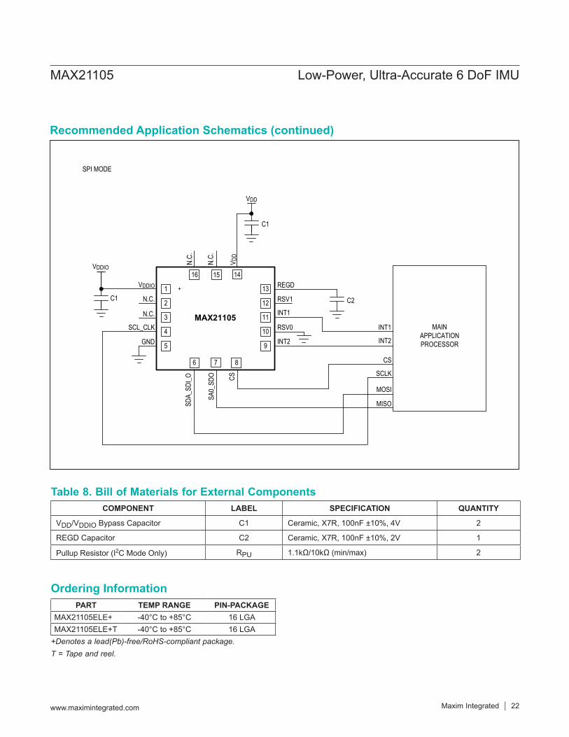
Table 8. Bill of Materials for External ComponentsCOMPONENT LABEL SPECIFICATION QUANTITY
VDD/VDDIO Bypass Capacitor C1 Ceramic, X7R, 100nF ±10%, 4V 2
REGD Capacitor C2 Ceramic, X7R, 100nF ±10%, 2V 1
Pullup Resistor (I2C Mode Only) RPU 1.1kΩ/10kΩ (min/max) 2
MAINAPPLICATIONPROCESSOR
MAX21105
1
2
3
4
5
6 7 8
13
12
11
10
9
16 15 14REGD
RSV1
N.C.
V DD
SCLK
MOSI
MISO
INT1
INT2
CS
N.C.
INT1
RSV0
INT2
CS
SA0_
SDO
SDA_
SDI_O
GND
SCL_CLK
N.C.
N.C.
VDDIO +
VDDIO
C1
VDD
C2
SPI MODE
C1
Ordering Information
Recommended Application Schematics (continued)
MAX21105 Low-Power, Ultra-Accurate 6 DoF IMU
www.maximintegrated.com Maxim Integrated 22
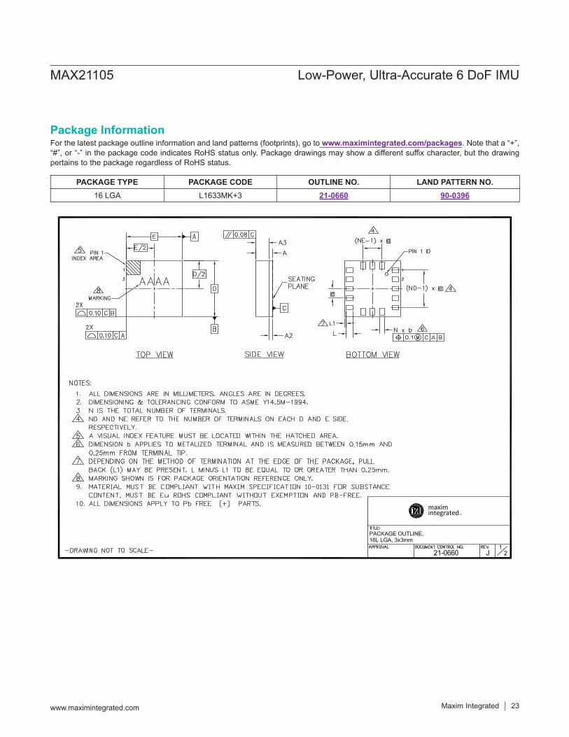
PACKAGE TYPE PACKAGE CODE OUTLINE NO. LAND PATTERN NO.16 LGA L1633MK+3 21-0660 90-0396
Package InformationFor the latest package outline information and land patterns (footprints), go to www.maximintegrated.com/packages. Note that a “+”, “#”, or “-” in the package code indicates RoHS status only. Package drawings may show a different suffix character, but the drawing pertains to the package regardless of RoHS status.
MAX21105 Low-Power, Ultra-Accurate 6 DoF IMU
www.maximintegrated.com Maxim Integrated 23

Package Information (continued)For the latest package outline information and land patterns (footprints), go to www.maximintegrated.com/packages. Note that a “+”, “#”, or “-” in the package code indicates RoHS status only. Package drawings may show a different suffix character, but the drawing pertains to the package regardless of RoHS status.
MAX21105 Low-Power, Ultra-Accurate 6 DoF IMU
www.maximintegrated.com Maxim Integrated 24

Package Information (continued)For the latest package outline information and land patterns (footprints), go to www.maximintegrated.com/packages. Note that a “+”, “#”, or “-” in the package code indicates RoHS status only. Package drawings may show a different suffix character, but the drawing pertains to the package regardless of RoHS status.
MAX21105 Low-Power, Ultra-Accurate 6 DoF IMU
www.maximintegrated.com Maxim Integrated 25
REVISION NUMBER
REVISION DATE DESCRIPTION PAGES
CHANGED0 12/14 Initial release —
Revision History
Maxim Integrated cannot assume responsibility for use of any circuitry other than circuitry entirely embodied in a Maxim Integrated product. No circuit patent licenses are implied. Maxim Integrated reserves the right to change the circuitry and specifications without notice at any time. The parametric values (min and max limits) shown in the Electrical Characteristics table are guaranteed. Other parametric values quoted in this data sheet are provided for guidance.
Maxim Integrated and the Maxim Integrated logo are trademarks of Maxim Integrated Products, Inc.
MAX21105 Low-Power, Ultra-Accurate 6 DoF IMU
© 2014 Maxim Integrated Products, Inc. 26
For pricing, delivery, and ordering information, please contact Maxim Direct at 1-888-629-4642, or visit Maxim Integrated’s website at www.maximintegrated.com.