Embed Size (px)
Citation preview

MAX 10 FPGA Configuration User Guide
Subscribe
Send Feedback
UG-M10CONFIG2015.12.14
101 Innovation DriveSan Jose, CA 95134www.altera.com

Contents
MAX 10 FPGA Configuration Overview............................................................ 1-1
MAX 10 FPGA Configuration Schemes and Features....................................... 2-1Configuration Schemes............................................................................................................................... 2-1
JTAG Configuration........................................................................................................................ 2-1Internal Configuration.................................................................................................................... 2-2
Configuration Features............................................................................................................................... 2-9Remote System Upgrade in Dual Compressed Images.............................................................. 2-9Configuration Design Security.....................................................................................................2-16SEU Mitigation and Configuration Error Detection................................................................ 2-19Configuration Data Compression............................................................................................... 2-23
Configuration Details................................................................................................................................2-24Configuration Sequence................................................................................................................2-24MAX 10 Configuration Pins.........................................................................................................2-26
MAX 10 FPGA Configuration Design Guidelines............................................. 3-1Dual-Purpose Configuration Pins............................................................................................................. 3-1
Guidelines: Dual-Purpose Configuration Pin..............................................................................3-1Enabling Dual-purpose Pin............................................................................................................ 3-2
Configuring MAX 10 Devices using JTAG Configuration.................................................................... 3-2JTAG Configuration Setup............................................................................................................. 3-3ICB Settings in JTAG Configuration.............................................................................................3-4
Configuring MAX 10 Devices using Internal Configuration................................................................ 3-4Selecting Internal Configuration Modes...................................................................................... 3-5.pof and ICB Settings....................................................................................................................... 3-5Programming .pof into Internal Flash.......................................................................................... 3-7
Error Detection............................................................................................................................................ 3-8Verifying Error Detection Functionality...................................................................................... 3-8Enabling Error Detection................................................................................................................3-8Accessing Error Detection Block Through User Interface........................................................ 3-9
Enabling Data Compression.....................................................................................................................3-12Enabling Compression Before Design Compilation.................................................................3-12Enabling Compression After Design Compilation................................................................... 3-12
AES Encryption..........................................................................................................................................3-13Generating .ekp File and Encrypt Configuration File.............................................................. 3-13Generating .jam/.jbc/.svf file from .ekp file................................................................................3-14Programming .ekp File and Encrypted POF File...................................................................... 3-15Encryption in Internal Configuration.........................................................................................3-16
MAX 10 FPGA Configuration IP Core Implementation Guides...................... 4-1
TOC-2
Altera Corporation

Altera Unique Chip ID IP Core................................................................................................................. 4-1Instantiating the Altera Unique Chip ID IP Core....................................................................... 4-1Resetting the Altera Unique Chip ID IP Core............................................................................. 4-1
Altera Dual Configuration IP Core........................................................................................................... 4-2Instantiating the Altera Dual Configuration IP Core................................................................. 4-2
Altera Dual Configuration IP Core References..................................................5-1Altera Dual Configuration IP Core Avalon-MM Address Map............................................................5-1Altera Dual Configuration IP Core Parameters...................................................................................... 5-3
Altera Unique Chip ID IP Core References........................................................6-1Altera Unique Chip ID IP Core Ports.......................................................................................................6-1
Additional Information for MAX 10 FPGA Configuration User Guide.......... A-1Document Revision History for MAX 10 FPGA Configuration User Guide.....................................A-1
TOC-3
Altera Corporation

MAX 10 FPGA Configuration Overview 12015.12.14
UG-M10CONFIG Subscribe Send Feedback
You can configure MAX® 10 configuration RAM (CRAM) using the following configuration schemes:
• JTAG configuration—using JTAG interface.• Internal configuration—using internal flash.
Supported Configuration Features
Table 1-1: Configuration Schemes and Features Supported by MAX 10 Devices
Configuration Scheme Remote SystemUpgrade Compression Design Security SEU Mitigation
JTAG configuration — — — YesInternal configuration Yes Yes Yes Yes
Related IP Cores
• Altera Dual Configuration IP Core—used in the remote system upgrade feature.• Altera Unique Chip ID IP Core—retrieves the chip ID of MAX 10 devices.
Related Information
• MAX 10 FPGA Configuration Schemes and Features on page 2-1Provides information about the configuration schemes and features.
• MAX 10 FPGA Configuration Design Guidelines on page 3-1Provides information about using the configuration schemes and features.
• Altera Unique Chip ID IP Core on page 2-17• Altera Dual Configuration IP Core on page 2-15
© 2015 Altera Corporation. All rights reserved. ALTERA, ARRIA, CYCLONE, ENPIRION, MAX, MEGACORE, NIOS, QUARTUS and STRATIX words and logos aretrademarks of Altera Corporation and registered in the U.S. Patent and Trademark Office and in other countries. All other words and logos identified astrademarks or service marks are the property of their respective holders as described at www.altera.com/common/legal.html. Altera warrants performanceof its semiconductor products to current specifications in accordance with Altera's standard warranty, but reserves the right to make changes to anyproducts and services at any time without notice. Altera assumes no responsibility or liability arising out of the application or use of any information,product, or service described herein except as expressly agreed to in writing by Altera. Altera customers are advised to obtain the latest version of devicespecifications before relying on any published information and before placing orders for products or services.
ISO9001:2008Registered
www.altera.com101 Innovation Drive, San Jose, CA 95134

MAX 10 FPGA Configuration Schemes andFeatures 2
2015.12.14
UG-M10CONFIG Subscribe Send Feedback
Configuration SchemesFigure 2-1: High-Level Overview of JTAG Configuration and Internal Configuration for MAX 10 Devices
CRAM
MAX 10 Device
JTAG In-System Programming
CFM
Configuration Data
InternalConfiguration
JTAG Configuration
.sof
.pof
JTAG ConfigurationIn MAX 10 devices, JTAG instructions take precedence over the internal configuration scheme.
Using the JTAG configuration scheme, you can directly configure the device CRAM through the JTAGinterface—TDI, TDO, TMS, and TCK pins. The Quartus® Prime software automatically generates an SRAMObject File (.sof). You can program the .sof using a download cable with the Quartus Prime softwareprogrammer.
Related InformationConfiguring MAX 10 Devices using JTAG Configuration on page 3-2Provides more information about JTAG configuration using download cable with Quartus Prime softwareprogrammer.
© 2015 Altera Corporation. All rights reserved. ALTERA, ARRIA, CYCLONE, ENPIRION, MAX, MEGACORE, NIOS, QUARTUS and STRATIX words and logos aretrademarks of Altera Corporation and registered in the U.S. Patent and Trademark Office and in other countries. All other words and logos identified astrademarks or service marks are the property of their respective holders as described at www.altera.com/common/legal.html. Altera warrants performanceof its semiconductor products to current specifications in accordance with Altera's standard warranty, but reserves the right to make changes to anyproducts and services at any time without notice. Altera assumes no responsibility or liability arising out of the application or use of any information,product, or service described herein except as expressly agreed to in writing by Altera. Altera customers are advised to obtain the latest version of devicespecifications before relying on any published information and before placing orders for products or services.
ISO9001:2008Registered
www.altera.com101 Innovation Drive, San Jose, CA 95134

JTAG Pins
Table 2-1: JTAG Pin
Pin Function Description
TDI Serial input pin for:
• instructions• test data• programming data
• TDI is sampled on the rising edge of TCK• TDI pins have internal weak pull-up resistors.
TDO Serial output pin for:
• instructions• test data• programming data
• TDO is sampled on the falling edge of TCK• The pin is tri-stated if data is not shifted out
of the device.
TMS Input pin that provides the controlsignal to determine the transitions ofthe TAP controller state machine.
• TMS is sampled on the rising edge of TCK• TMS pins have internal weak pull-up resistors.
TCK Clock input to the BST circuitry. —
All the JTAG pins are powered by the VCCIO 1B. In JTAG mode, the I/O pins support the LVTTL/LVCMOS 3.3-1.5V standards.
Related Information
• MAX 10 Device DatasheetProvides more information about supported I/O standard in MAX 10 devices.
• Guidelines: Dual-Purpose Configuration Pin on page 3-1• Enabling Dual-purpose Pin on page 3-2
Internal ConfigurationYou need to program the configuration data into the configuration flash memory (CFM) before internalconfiguration can take place. The configuration data to be written to CFM will be part of the programmerobject file (.pof). Using JTAG In-System Programming (ISP), you can program the .pof into the internalflash.
During internal configuration, MAX 10 devices load the CRAM with configuration data from the CFM.
Internal Configuration Modes
Table 2-2: Supported Internal Configuration Modes Based on MAX 10 Feature Options
MAX 10 Feature Options Supported Internal Configuration Mode
Compact • Single Compressed Image• Single Uncompressed Image
2-2 JTAG PinsUG-M10CONFIG
2015.12.14
Altera Corporation MAX 10 FPGA Configuration Schemes and Features
Send Feedback

MAX 10 Feature Options Supported Internal Configuration Mode
Analog
• Dual Compressed Images• Single Compressed Image• Single Compressed Image with Memory Initialization• Single Uncompressed Image• Single Uncompressed Image with Memory Initialization
Note: In dual compressed images mode, you can use the CONFIG_SEL pin to select the configurationimage.
Related Information
• Configuring MAX 10 Devices using Internal Configuration on page 3-4• Remote System Upgrade in Dual Compressed Images on page 2-9
Configuration Flash Memory
The CFM is a non-volatile internal flash that is used to store configuration images. The CFM may store upto two compressed configuration images, depending on the compression and the MAX 10 devices. Thecompression ratio for the configuration image should be at least 30% for the device to be able store twoconfiguration images.
Related InformationConfiguration Flash Memory Permissions on page 2-19
Configuration Flash Memory Sectors
All CFM in MAX 10 devices consist of three sectors, CFM0, CFM1, and CFM2 except for the 10M02. Thesectors are programmed differently depending on the internal configuration mode you select.
The 10M02 device consists of only CFM0. The CFM0 sector in 10M02 devices is programmed similarlywhen you select single compressed image or single uncompressed image.
UG-M10CONFIG2015.12.14 Configuration Flash Memory 2-3
MAX 10 FPGA Configuration Schemes and Features Altera Corporation
Send Feedback

Figure 2-2: Configuration Flash Memory Sectors Utilization for all MAX 10 with Analog Feature Options
Unutilized CFM1 and CFM2 sectors can be used for additional user flash memory (UFM).
Configuration Flash Memory Sectors
CFM0CFM1CFM2
Dual Compressed Image
Single Uncompressed Image
Single Uncompressed Imagewith Memory Initialization
Single Compressed Imagewith Memory Initialization
Single Compressed Image
Compressed Image 0
Uncompressed Image 0 with Memory Initialization
Compressed Image 0 with Memory Initialization
Compressed Image 0
Uncompressed Image 0
Compressed Image 1
User Flash Memory
User Flash Memory
Internal ConfigurationMode
Related InformationCFM and UFM Array Size
Configuration Flash Memory Programming Time
Table 2-3: Configuration Flash Memory Programming Time for Sectors in MAX 10 Devices
Note: The programming time reflects JTAG interface programming time only without any system overhead. Itdoes not reflect the actual programming time that you face. To compensate the system overhead, QuartusPrime Programmer is enhanced to utilize flash parallel mode during device programming for MAX 1010M04/08/16/25/40/50 devices. The 10M02 device does not support flash parallel mode, user mayexperience relatively slow programming time if compare to other device.
DeviceProgramming Time (s)
CFM2 CFM1 CFM0
10M02 — — 5.4
10M04 6.5 4.6 11.1
10M08 12.0 8.9 20.8
10M16 and 10M25 16.4 12.6 29.0
10M40 and 10M50 30.2 22.7 52.9
In-System ProgrammingYou can program the internal flash including the CFM of MAX 10 devices with ISP through industrystandard JTAG interface. ISP offers the capability to program, erase, and verify the CFM. The JTAGcircuitry and ISP instructions for MAX 10 devices are compliant to the IEEE-1532-2002 programmingspecification.
2-4 Configuration Flash Memory Programming TimeUG-M10CONFIG
2015.12.14
Altera Corporation MAX 10 FPGA Configuration Schemes and Features
Send Feedback

During ISP, the MAX 10 receives the IEEE Std. 1532 instructions, addresses, and data through the TDIinput pin. Data is shifted out through the TDO output pin and compared with the expected data.
The following are the generic flow of an ISP operation:
1. Check ID—the JTAG ID is checked before any program or verify process. The time required to readthis JTAG ID is relatively small compared to the overall programming time.
2. Enter ISP—ensures the I/O pins transition smoothly from user mode to the ISP mode.3. Sector Erase—shifting in the address and instruction to erase the device and applying erase pulses.4. Program—shifting in the address, data, and program instructions and generating the program pulse to
program the flash cells. This process is repeated for each address in the internal flash sector.5. Verify—shifting in addresses, applying the verify instruction to generate the read pulse, and shifting
out the data for comparison. This process is repeated for each internal flash address.6. Exit ISP—ensures that the I/O pins transition smoothly from the ISP mode to the user mode.
You can also use the Quartus Prime Programmer to program the CFM.
Related InformationProgramming .pof into Internal Flash on page 3-7Provides the steps to program the .pof using Quartus Prime Programmer.
ISP ClampWhen a normal ISP operation begins, all I/O pins are tri-stated. For situations when the I/O pins of thedevice should not be tri-stated when the device is in ISP operation, you can use the ISP clamp feature.
The ISP clamp feature allows you to use the Quartus Prime software to hold each MAX 10 I/O pins to astatic state when you program the device. After you successfully program the device in ISP clamp mode,the I/O pins are released and the device functions according to the new design.
You can set the ISP clamp through Device and Pin Option, or Pin Assignment tool.
Real-Time ISP
In a normal ISP operation, to update the internal flash with a new design image, the device exits from usermode and all I/O pins remain tri-stated. After the device completes programing the new design image, itresets and enters user mode.
The real-time ISP feature updates the internal flash with a new design image while operating in usermode. During the internal flash programming, the device continues to operate using the existing design.After the new design image programming process completes, the device will not reset. The new designimage update only takes effect in the next reconfiguration cycle.
UG-M10CONFIG2015.12.14 ISP Clamp 2-5
MAX 10 FPGA Configuration Schemes and Features Altera Corporation
Send Feedback

ISP and Real-Time ISP Instructions
Table 2-4: ISP and Real-Time ISP Instructions for MAX 10 Devices
Instruction Instruction Code Description
CONFIG_IO 00 0000 1101 • Allows I/O reconfiguration through JTAG ports usingthe IOCSR for JTAG testing. This is executed after orduring configurations.
• nSTATUS pin must go high before you can issue theCONFIG_IO instruction.
PULSE_NCONFIG 00 0000 0001 Emulates pulsing the nCONFIG pin low to trigger reconfi‐guration even though the physical pin is unaffected.
ISC_ENABLE_HIZ (1) 10 1100 1100 • Puts the device in ISP mode, tri-states all I/O pins,and drives all core drivers, logic, and registers.
• Device remains in the ISP mode until the ISC_DISABLE instruction is loaded and updated.
• The ISC_ENABLE instruction is a mandatory instruc‐tion. This requirement is met by the ISC_ENABLE_CLAMP or ISC_ENABLE_HIZ instruction.
ISC_ENABLE_CLAMP (1) 10 0011 0011 • Puts the device in ISP mode and forces all I/O pins tofollow the contents of the JTAG boundary-scanregister.
• When this instruction is activated, all core drivers,logics, and registers are frozen. The I/O pins remainclamped until the device exits ISP mode successfully.
ISC_DISABLE 10 0000 0001 • Brings the device out of ISP mode.• Successful completion of the ISC_DISABLE instruction
happens immediately after waiting 200 µs in the Run-Test/Idle state.
ISC_PROGRAM(2) 10 1111 0100 Sets the device up for in-system programming. Program‐ming occurs in the run-test or idle state.
ISC_NOOP(2) 10 0001 0000 • Sets the device to a no-operation mode withoutleaving the ISP mode and targets the ISC_Defaultregister.
• Use when:
• two or more ISP-compliant devices are beingaccessed in ISP mode and;
• a subset of the devices perform some instructionswhile other more complex devices are completingextra steps in a given process.
(1) Do not issue the ISC_ENABLE_HIZ and ISC_ENABLE_CLAMP instructions from the core logic.(2) All ISP and real-time ISP instructions are disabled when the device is not in the ISP or real-time ISP mode,
except for the enabling and disabling instructions.
2-6 ISP and Real-Time ISP InstructionsUG-M10CONFIG
2015.12.14
Altera Corporation MAX 10 FPGA Configuration Schemes and Features
Send Feedback

Instruction Instruction Code Description
ISC_ADDRESS_SHIFT(2) 10 0000 0011 Sets the device up to load the flash address. It targets theISC_Address register, which is the flash address register.
ISC_ERASE(2) 10 1111 0010 • Sets the device up to erase the internal flash.• Issue after ISC_ADDRESS_SHIFT instruction.
ISC_READ(2) 10 0000 0101 • Sets the device up for verifying the internal flashunder normal user bias conditions.
• The ISC_READ instruction supports explicitaddressing and auto-increment, also known as theBurst mode.
BGP_ENABLE 01 1001 1001 • Sets the device to the real-time ISP mode.• Allows access to the internal flash configuration
sector while the device is still in user mode.
BGP_DISABLE 01 0110 0110 • Brings the device out of the real-time ISP mode.• The device has to exit the real-time ISP mode using
the BGP_DISABLE instruction after it is interrupted byreconfiguration.
Caution: Do not use unsupported JTAG instructions. It will put the device into an unknown state andrequires a power cycle to recover the operation.
Initialization Configuration BitsInitialization Configuration Bits (ICB) stores the configuration feature settings of the MAX 10 device. Youcan set the ICB settings during Convert Programming File.
Table 2-5: ICB Values and Descriptions for MAX 10 Devices
Configuration Settings Description Default State/Value
Power On Reset Scheme Specifies device Power On Reset (POR) scheme:
• Instant ON• Fast POR delay• Slow POR delay
Instant ON
Set I/O to weak pull-up priorusermode
• Enable: Sets I/O to weak pull-up during deviceconfiguration.
• Disable: Tri-states I/O input.
Enable
UG-M10CONFIG2015.12.14 Initialization Configuration Bits 2-7
MAX 10 FPGA Configuration Schemes and Features Altera Corporation
Send Feedback

Configuration Settings Description Default State/Value
Configure device from CFM0only.
Enable:
• CONFIG_SEL pin setting is disabled.• Device automatically loads image 0.• Device does not load image 1 if image 0 fails.
Disable:
• Device automatically loads secondary image ifinitial image fails.
Disable
Use secondary image ISP dataas default setting whenavailable.
Select ISP data from initial or primary image toinclude in the POF.
• Disable: Use ISP data from initial image• Enable: Use ISP data from primary image
ISP data contains the information about state ofthe pin during ISP. This can be either tri-state withweak pull-up or clamp the I/O state. You can setthe ISP clamp through Device and Pin Option, orPin Assignment tool.
Disable
Verify Protect To disable or enable the Verify Protect feature. Disable
Allow encrypted POF only If enabled, configuration error will occur ifunencrypted .pof is used.
Disable
JTAG Secure(3) To disable or enable the JTAG Secure feature. Disable
Enable Watchdog To disable or enable the watchdog timer forremote system upgrade.
Enable
Watchdog value To set the watchdog timer value for remote systemupgrade.
0x1FFF(4)
Related Information
• .pof and ICB Settings on page 3-5• .pof Generation through Convert Programming Files
Provides more information about setting the ICB during .pof generation using Convert ProgrammingFile.
• Instant-on on page 2-25Provides more information about Instant ON and other power on reset scheme.
• Verify Protect on page 2-18• JTAG Secure Mode on page 2-17
(3) The JTAG Secure feature will be disabled by default in Quartus Prime. If you are interested in using theJTAG Secure feature, contact Altera for support.
(4) The watchdog timer value depends on the MAX 10 you are using. Refer to the Watchdog Timer section formore information.
2-8 Initialization Configuration BitsUG-M10CONFIG
2015.12.14
Altera Corporation MAX 10 FPGA Configuration Schemes and Features
Send Feedback

• ISP and Real-Time ISP Instructions on page 2-6• User Watchdog Timer on page 2-15
Configuration Features
Remote System Upgrade in Dual Compressed ImagesMAX 10 devices support the remote system upgrade feature. By default, the remote system upgradefeature is enabled in all MAX 10 devices when you select the dual compressed image internalconfiguration mode.
The remote system upgrade feature in MAX 10 devices offers the following capabilities:
• Manages remote configuration• Provides error detection, recovery, and information• Supports direct-to-application configuration image• Supports compressed and encrypted .pof
You can use the Altera Dual Configuration IP core or the remote system upgrade circuitry to access theremote system upgrade block in MAX 10 devices.
Related InformationAN 741: Remote System Upgrade for MAX 10 FPGA Devices over UART with the Nios II ProcessorProvides reference design for remote system upgrade in MAX 10 FPGA devices.
Remote System Upgrade FlowBoth the application configuration images, image 0 and image 1, are stored in the CFM. The MAX 10device loads either one of the application configuration image from the CFM.
UG-M10CONFIG2015.12.14 Configuration Features 2-9
MAX 10 FPGA Configuration Schemes and Features Altera Corporation
Send Feedback
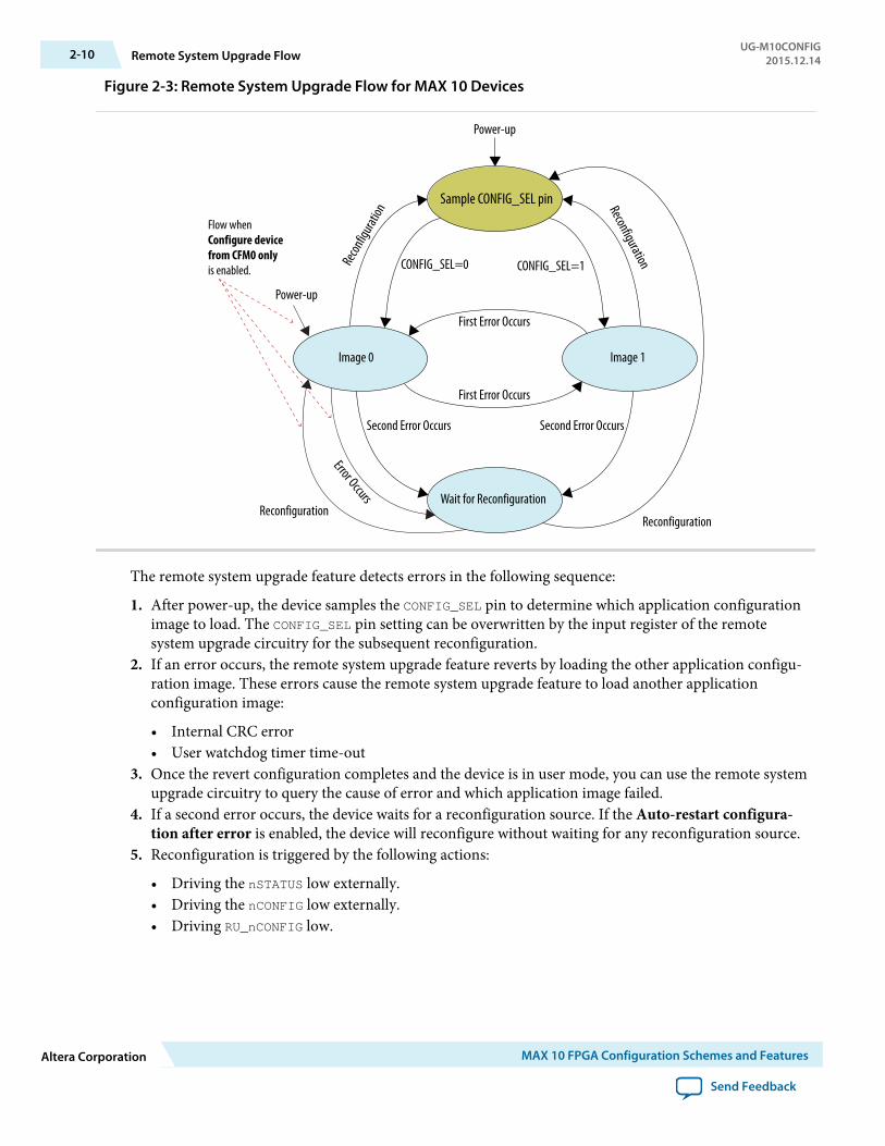
Figure 2-3: Remote System Upgrade Flow for MAX 10 Devices
Sample CONFIG_SEL pin
Image 0 Image 1
CONFIG_SEL=0 CONFIG_SEL=1
Wait for Reconfiguration
Power-up
ReconfigurationRecon
figura
tion
First Error Occurs
First Error Occurs
Second Error Occurs
Flow whenConfigure devicefrom CFM0 onlyis enabled.
Second Error Occurs
Error OccursReconfiguration
Reconfiguration
Power-up
The remote system upgrade feature detects errors in the following sequence:
1. After power-up, the device samples the CONFIG_SEL pin to determine which application configurationimage to load. The CONFIG_SEL pin setting can be overwritten by the input register of the remotesystem upgrade circuitry for the subsequent reconfiguration.
2. If an error occurs, the remote system upgrade feature reverts by loading the other application configu‐ration image. These errors cause the remote system upgrade feature to load another applicationconfiguration image:
• Internal CRC error• User watchdog timer time-out
3. Once the revert configuration completes and the device is in user mode, you can use the remote systemupgrade circuitry to query the cause of error and which application image failed.
4. If a second error occurs, the device waits for a reconfiguration source. If the Auto-restart configura‐tion after error is enabled, the device will reconfigure without waiting for any reconfiguration source.
5. Reconfiguration is triggered by the following actions:
• Driving the nSTATUS low externally.• Driving the nCONFIG low externally.• Driving RU_nCONFIG low.
2-10 Remote System Upgrade FlowUG-M10CONFIG
2015.12.14
Altera Corporation MAX 10 FPGA Configuration Schemes and Features
Send Feedback
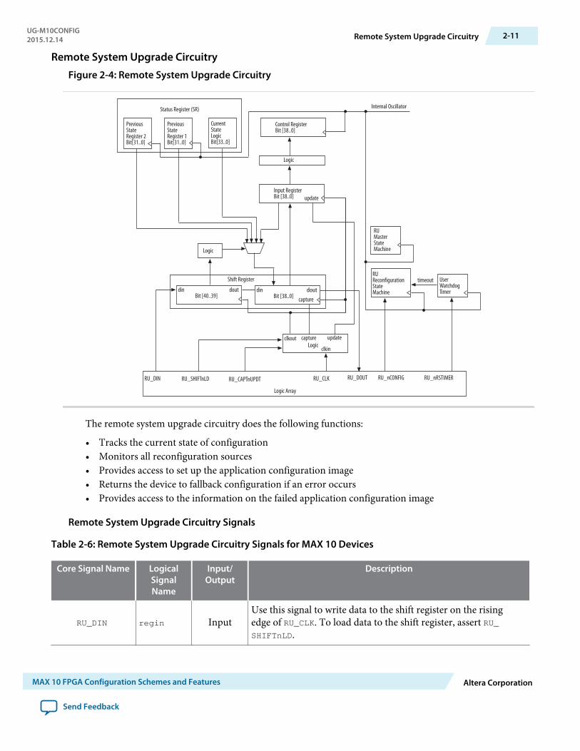
Remote System Upgrade Circuitry
Figure 2-4: Remote System Upgrade Circuitry
Status Register (SR)
PreviousStateRegister 2Bit[31..0]
StateRegister 1Bit[31..0]
CurrentStateLogicBit[33..0]
Internal Oscillator
Control RegisterBit [38..0]
Logic
Input RegisterBit [38..0] update
Logic
Bit [40..39]doutdin
Bit [38..0]doutdin
capture
Shift Register
clkout capture updateLogic
clkin
RU_DIN RU_SHIFTnLD RU_CAPTnUPDT RU_CLK RU_nRSTIMER
Logic Array
RUReconfigurationStateMachine
User WatchdogTimer
RUMasterStateMachine
timeout
RU_nCONFIGRU_DOUT
Previous
The remote system upgrade circuitry does the following functions:
• Tracks the current state of configuration• Monitors all reconfiguration sources• Provides access to set up the application configuration image• Returns the device to fallback configuration if an error occurs• Provides access to the information on the failed application configuration image
Remote System Upgrade Circuitry Signals
Table 2-6: Remote System Upgrade Circuitry Signals for MAX 10 Devices
Core Signal Name LogicalSignalName
Input/Output
Description
RU_DIN regin InputUse this signal to write data to the shift register on the risingedge of RU_CLK. To load data to the shift register, assert RU_SHIFTnLD.
UG-M10CONFIG2015.12.14 Remote System Upgrade Circuitry 2-11
MAX 10 FPGA Configuration Schemes and Features Altera Corporation
Send Feedback

Core Signal Name LogicalSignalName
Input/Output
Description
RU_DOUT regout OutputUse this signal to get output data from the shift register. Datais clocked out on each rising edge of RU_CLK if RU_SHIFTnLD isasserted.
RU_nRSTIMER rsttimer Input
• Use this signal to reset the user watchdog timer. A fallingedge of this signal triggers a reset of the user watchdogtimer.
• To reset the timer, pulse the RU_nRSTIMER signal for aminimum of 250 ns.
RU_nCONFIG rconfig InputUse this signal to reconfigure the device. Driving this signallow triggers the device to reconfigure if you enable the remotesystem upgrade feature.
RU_CLK clk Input
The clock to the remote system upgrade circuitry. All registersin this clock domain are enabled in user mode if you enablethe remote system upgrade. Shift register and input registerare positive edge flip-flops.
RU_SHIFTnLD shiftnld Input Control signals that determine the mode of remote systemupgrade circuitry.
• When RU_SHIFTnLD is driven low and RU_CAPTnUPDT isdriven low, the input register is loaded with the contents ofthe shift register on the rising edge of RU_CLK.
• When RU_SHIFTnLD is driven low and RU_CAPTnUPDT isdriven high, the shift register captures values from theinput_cs_ps module on the rising edge of RU_CLK.
• When RU_SHIFTnLD is driven high, the RU_CAPTnUPDT willbe ignored and the shift register shifts data on each risingedge of RU_CLK.
RU_CAPTnUPDT captnupdt Input
Related Information
• Accessing the Remote System Upgrade Block Through User InterfaceProvides more information about accessing the remote system upgrade through user interface atom.
• MAX 10 Device DatasheetProvides more information about Remote System Upgrade timing specifications.
Remote System Upgrade Circuitry Input Control
The remote system upgrade circuitry has three modes of operation.
• Update—loads the values in the shift register into the input register.• Capture—loads the shift register with data to be shifted out.• Shift—shifts out data to the user logic.
2-12 Remote System Upgrade Circuitry Input ControlUG-M10CONFIG
2015.12.14
Altera Corporation MAX 10 FPGA Configuration Schemes and Features
Send Feedback

Table 2-7: Control Inputs to the Remote System Upgrade Circuitry
Remote System Upgrade Circuitry Control InputsOperation
Mode
Input Settings for Registers
RU_SHIFTnLD RU_CAPTnUPDT Shift register[40]
Shift register[39]
ShiftRegister[38:0]
InputRegister[38:0]
0 0 Don't Care Don't Care Update Shift Register[38:0]
Shift Register[38:0]
0 1 0 0 Capture Current State InputRegister[38:0]
0 1 0 1 Capture8’b0,
Previous StateApplication1
InputRegister[38:0]
0 1 1 0 Capture8’b0,
Previous StateApplication2
InputRegister[38:0]
0 1 1 1 Capture InputRegister[38:0]
InputRegister[38:0]
1 Don't Care Don't Care Don't Care Shiftru_din, Shift
Register[38:1]
InputRegister[38:0]
The following shows examples of driving the control inputs in the remote system upgrade circuitry:
• When you drive RU_SHIFTnLD high to 1’b1, the shift register shifts data on each rising edge of RU_CLKand RU_CAPTnUPDT has no function.
• When you drive both RU_SHIFTnLD and RU_CAPTnUPDT low to 1’b0, the input register is loaded withthe contents of the shift register on the rising edge of RU_CLK.
• When you drive RU_SHIFTnLD low to 1’b0 and RU_CAPTnUPDT high to 1’b1, the shift registercaptures values on the rising edge of RU_DCLK.
Remote System Upgrade Input Register
Table 2-8: Remote System Upgrade Input Register for MAX 10 Devices
Bits Name Description
38:14 Reserved Reserved—set to 0.
13 ru_config_sel
• 0: Load configuration image 0• 1: Load configuration image 1
This bit will only work if the ru_config_sel_overwrite bit is setto 1.
12 ru_config_sel_
overwrite
• 0: Disable overwrite CONFIG_SEL pin• 1: Enable overwrite CONFIG_SEL pin
UG-M10CONFIG2015.12.14 Remote System Upgrade Input Register 2-13
MAX 10 FPGA Configuration Schemes and Features Altera Corporation
Send Feedback

Bits Name Description
11:0 Reserved Reserved—set to 0.
Remote System Upgrade Status Registers
Table 2-9: Remote System Upgrade Status Register—Current State Logic Bit for MAX 10 Devices
Bits Name Description
33:30 msm_cs The current state of the master state machine (MSM).
29 ru_wd_enThe current state of the enabled user watchdog timer. The defaultstate is active high.
28:0 wd_timeout_value The current, entire 29-bit watchdog time-out value.
Table 2-10: Remote System Upgrade Status Register—Previous State Bit for MAX 10 Devices
Bits Name Description
31 nconfig An active high field that describes the reconfiguration sourceswhich caused the MAX 10 device to leave the previous applicationconfiguration. In the event of a tie, the higher bit order takesprecedence. For example, if the nconfig and the ru_nconfigtriggered at the same time, the nconfig takes precedence over theru_nconfig.
30 crcerror
29 nstatus
28 wdtimer
27:26 Reserved Reserved—set to 0.
25:22 msm_cs
The state of the MSM when a reconfiguration event occurred. Thereconfiguration will cause the device to leave the previous applica‐tion configuration.
21:0 Reserved Reserved—set to 0.
Related InformationAltera Dual Configuration IP Core Avalon-MM Address Map on page 5-1
Master State Machine
The master state machine (MSM) tracks current configuration mode and enables the user watchdogtimer.
Table 2-11: Remote System Upgrade Master State Machine Current State Descriptions for MAX 10 Devices
msm_cs Values State Description
0010 Image 0 is being loaded.
0011 Image 1 is being loaded after a revert in application image happens.
0100 Image 1 is being loaded.
0101 Image 0 is being loaded after a revert in application image happens.
2-14 Remote System Upgrade Status RegistersUG-M10CONFIG
2015.12.14
Altera Corporation MAX 10 FPGA Configuration Schemes and Features
Send Feedback
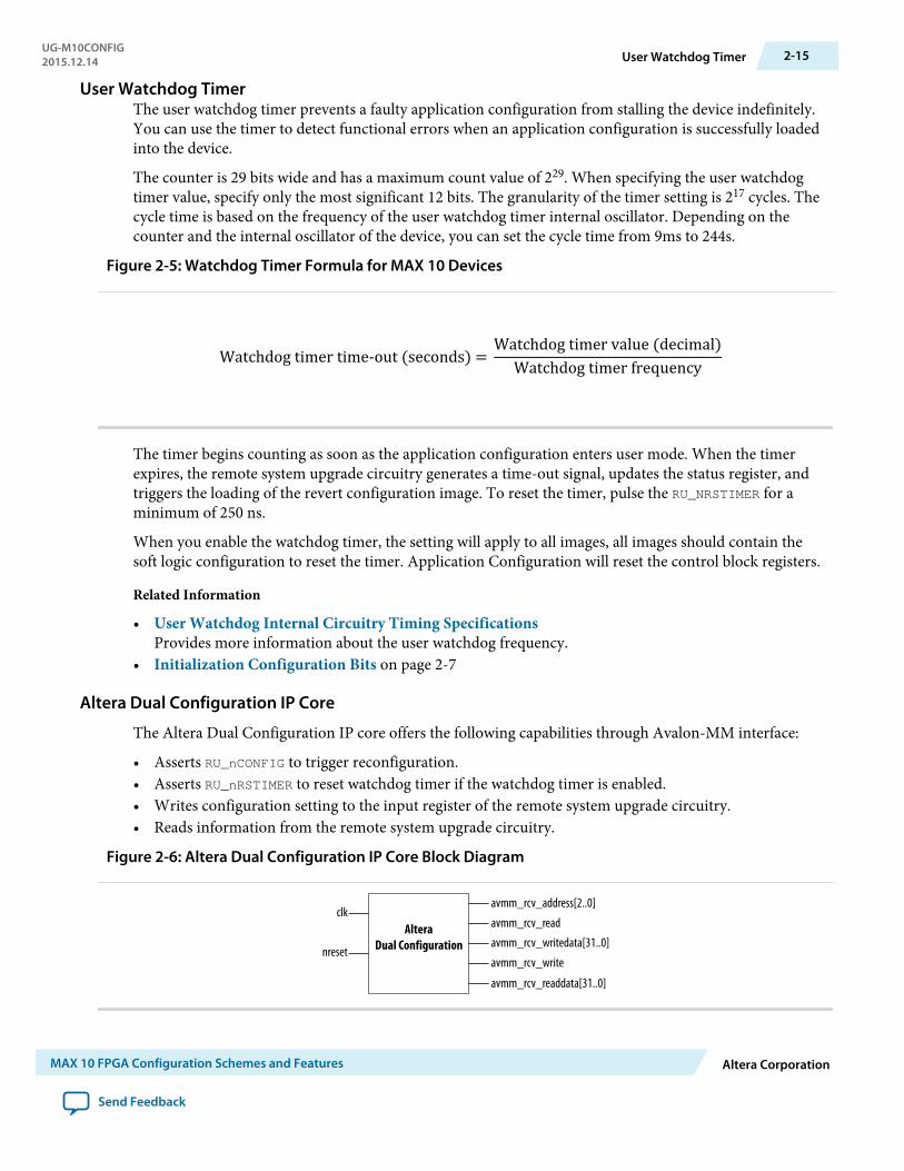
User Watchdog TimerThe user watchdog timer prevents a faulty application configuration from stalling the device indefinitely.You can use the timer to detect functional errors when an application configuration is successfully loadedinto the device.
The counter is 29 bits wide and has a maximum count value of 229. When specifying the user watchdogtimer value, specify only the most significant 12 bits. The granularity of the timer setting is 217 cycles. Thecycle time is based on the frequency of the user watchdog timer internal oscillator. Depending on thecounter and the internal oscillator of the device, you can set the cycle time from 9ms to 244s.
Figure 2-5: Watchdog Timer Formula for MAX 10 Devices
The timer begins counting as soon as the application configuration enters user mode. When the timerexpires, the remote system upgrade circuitry generates a time-out signal, updates the status register, andtriggers the loading of the revert configuration image. To reset the timer, pulse the RU_NRSTIMER for aminimum of 250 ns.
When you enable the watchdog timer, the setting will apply to all images, all images should contain thesoft logic configuration to reset the timer. Application Configuration will reset the control block registers.
Related Information
• User Watchdog Internal Circuitry Timing SpecificationsProvides more information about the user watchdog frequency.
• Initialization Configuration Bits on page 2-7
Altera Dual Configuration IP Core
The Altera Dual Configuration IP core offers the following capabilities through Avalon-MM interface:
• Asserts RU_nCONFIG to trigger reconfiguration.• Asserts RU_nRSTIMER to reset watchdog timer if the watchdog timer is enabled.• Writes configuration setting to the input register of the remote system upgrade circuitry.• Reads information from the remote system upgrade circuitry.
Figure 2-6: Altera Dual Configuration IP Core Block Diagram
AlteraDual Configuration
clk
nreset
avmm_rcv_address[2..0]
avmm_rcv_read
avmm_rcv_writedata[31..0]
avmm_rcv_write
avmm_rcv_readdata[31..0]
UG-M10CONFIG2015.12.14 User Watchdog Timer 2-15
MAX 10 FPGA Configuration Schemes and Features Altera Corporation
Send Feedback

Related Information
• Altera Dual Configuration IP Core Avalon-MM Address Map on page 5-1• Avalon Interface Specifications
Provides more information about the Avalon-MM interface specifications applied in Altera DualConfiguration IP Core.
• Instantiating the Altera Dual Configuration IP Core on page 4-2• Accessing the Remote System Upgrade Block Through User Interface
Configuration Design SecurityThe MAX 10 design security feature supports the following capabilities:
• Encryption—Built-in encryption standard (AES) to support 128-bit key industry-standard designsecurity algorithm
• Chip ID—Unique device identification• JTAG secure mode—limits access to JTAG instructions• Verify Protect—allows optional disabling of CFM content read-back
AES Encryption Protection
The MAX 10 design security feature provides the following security protection for your designs:
• Security against copying—the non-volatile key is securely stored in the MAX 10 devices and cannot beread through any interface. Without this key, attacker will not be able to decrypt the encryptedconfiguration image.
• Security against reverse engineering—reverse engineering from an encrypted configuration file is verydifficult and time consuming because the file require decryption.
• Security against tampering—after you enable the JTAG Secure and Encrypted POF (EPOF) only, theMAX 10 device can only accept configuration files encrypted with the same key. Additionally, configu‐ration through the JTAG interface is blocked.
Related Information.pof Generation through Convert Programming Files
Encryption and Decryption
MAX 10 supports AES encryption. Programming bitstream is encrypted based on the encryption key thatis specified by user. In MAX 10 devices, the key is part of the ICB settings stored in the internal flash.Hence, the key will be non-volatile but user can clear/delete the key by a full chip erase the device.
When you use compression with encryption, the configuration file is first compressed, and thenencrypted using the Quartus Prime software. During configuration, the device first decrypts, and thendecompresses the configuration file.
The header and I/O configuration shift register (IOCSR) data will not be encrypted. The decryption blockis activated after the IOCSR chain is programmed. The decryption block only decrypts core data andpostamble.
Related InformationJTAG Instruction Availability on page 2-18
2-16 Configuration Design SecurityUG-M10CONFIG
2015.12.14
Altera Corporation MAX 10 FPGA Configuration Schemes and Features
Send Feedback

Unique Chip ID
Unique chip ID provides the following features:
• Identifies your device in your design as part of a security feature to protect your design from anunauthorized device.
• Provides non-volatile 64-bits unique ID for each MAX 10 device with write protection.
You can use the Altera Unique Chip ID IP core to acquire the chip ID of your MAX 10 device.
Related Information
• Altera Unique Chip ID IP Core on page 4-1• Altera Unique Chip ID IP Core Ports on page 6-1
Altera Unique Chip ID IP Core
Figure 2-7: Altera Unique Chip ID IP Core Block Diagram
Altera UniqueChip ID
clkin data_valid
chip_id[63..0]reset
At the initial state, the data_valid signal is low because no data is read from the unique chip ID block.After feeding a clock signal to the clkin input port, the Altera Unique Chip ID IP core begins to acquirethe chip ID of your device through the unique chip ID block. After acquiring the chip ID of your device,the Altera Unique Chip ID IP core asserts the data_valid signal to indicate that the chip ID value at theoutput port is ready for retrieval.
The operation repeats only when you provide another clock signal when the data_valid signal is low. Ifthe data_valid signal is high when you provide another clock signal, the operation stops because thechip_id[63..0] output holds the chip ID of your device.
A minimum of 67 clock cycles are required for the data_valid signal to go high.
The chip_id[63:0]output port holds the value of chip ID of your device until you reconfigure the deviceor reset the Altera Unique Chip ID IP core.
JTAG Secure ModeIn JTAG Secure mode, the device only allows mandatory JTAG 1149.1 instructions to be exercised.
You can enable the JTAG secure when generating the .pof in the Convert Programming Files. To exit JTAGsecure mode, issue the UNLOCK JTAG instruction. The LOCK JTAG instruction puts the device in the JTAGsecure mode again. The LOCK and UNLOCK JTAG instructions can only be issued through the JTAG coreaccess.
UG-M10CONFIG2015.12.14 Unique Chip ID 2-17
MAX 10 FPGA Configuration Schemes and Features Altera Corporation
Send Feedback

Related Information
• JTAG Instruction Availability on page 2-18• Configuration Flash Memory Permissions on page 2-19• .pof Generation through Convert Programming Files
JTAG Secure Mode Instructions
Table 2-12: JTAG Secure Mode Instructions for MAX 10 Devices
JTAG Instruction Instruction Code Description
LOCK 10 0000 0010 • Activates the JTAG secure mode.• Blocks access from both external pins and core to
JTAG.
UNLOCK 10 0000 1000 Deactivates the JTAG secure mode.
Verify ProtectVerify Protect is a security feature to enhance CFM security. When you enable the Verify Protect, onlyprogram and erase operation are allowed on the CFM. This capability protects the CFM contents frombeing copied.
You can turn on the Verify Protect feature by enabling the Verify Protect in the Quartus Primeprogrammer.
Related InformationConfiguration Flash Memory Permissions on page 2-19
JTAG Instruction Availability
Table 2-13: JTAG Instruction Availability Based on JTAG Secure Mode and Encryption Settings
JTAG Secure Mode Encryption Description
Disabled
Disabled All JTAG Instructions enabled
EnabledAll JTAG Instructions are enabled except:
• CONFIGURE
Enabled
Disabled All JTAG Instructions are disabled except:
• SAMPLE/PRELOAD
• BYPASS
• EXTEST
• IDCODE
• UNLOCK
• LOCK
Enabled
2-18 JTAG Secure Mode InstructionsUG-M10CONFIG
2015.12.14
Altera Corporation MAX 10 FPGA Configuration Schemes and Features
Send Feedback

Related Information
• JTAG Secure Mode on page 2-17• Encryption and Decryption on page 2-16
Configuration Flash Memory PermissionsThe JTAG secure mode and verify protect features determines the CFM operation permission.. The tablelist the operations permitted based on the security settings.
Table 2-14: CFM Permissions for MAX 10 Devices
Operation
JTAG Secure Mode Disabled JTAG Secure Mode Enabled
Verify ProtectDisabled
Verify ProtectEnabled
Verify ProtectDisabled
Verify ProtectEnabled
ISP through core Illegal operation Illegal operation Illegal operation Illegal operation
ISP throughJTAG pins Full access Program and erase
only No access No access
Real-time ISPthrough core Full access Program and erase
only No access No access
Real-time ISPthrough JTAGpins
Full access Program and eraseonly No access No access
UFM interfacethrough core(5) Full access Full access Full access Full access
Related Information
• JTAG Secure Mode on page 2-17• Verify Protect on page 2-18
SEU Mitigation and Configuration Error DetectionThe dedicated circuitry built in MAX 10 devices consists of an error detection cyclic redundancy check(EDCRC) feature. You can use this feature to mitigate single-event upset (SEU) or soft errors.
The hardened on-chip EDCRC circuitry allows you to perform the following operations without anyimpact on the fitting of the device:
• Auto-detection of cyclic redundancy check (CRC) errors during configuration.• Identification of SEU in user mode with the optional CRC error detection.• Testing of error detection by error detection verification through the JTAG interface.
Related Information
• Verifying Error Detection Functionality on page 3-8• Enabling Error Detection on page 3-8• Accessing Error Detection Block Through User Interface on page 3-9
(5) The UFM interface through core is available if you select the dual compressed image mode.
UG-M10CONFIG2015.12.14 Configuration Flash Memory Permissions 2-19
MAX 10 FPGA Configuration Schemes and Features Altera Corporation
Send Feedback

Configuration Error DetectionIn configuration mode, a frame-based CRC is stored in the configuration data and contains the CRC valuefor each data frame.
During configuration, the MAX 10 device calculates the CRC value based on the frame of data that isreceived and compares it against the frame CRC value in the data stream. Configuration continues untilthe device detects an error or when all the values are calculated.
For MAX 10 devices, the CRC is computed by the Quartus Prime software and downloaded into thedevice as part of the configuration bit stream. These devices store the CRC in the 32-bit storage register atthe end of the configuration mode.
User Mode Error DetectionSEUs are changes in a CRAM bit state due to an ionizing particle. MAX 10 devices have built-in errordetection circuitry to detect data corruption in the CRAM cells.
This error detection capability continuously computes the CRC of the configured CRAM bits. The CRC ofthe contents of the device are compared with the pre-calculated CRC value obtained at the end of theconfiguration. If the CRC values match, there is no error in the current configuration CRAM bits. Theprocess of error detection continues until the device is reset—by setting nCONFIG to low.
The error detection circuitry in MAX 10 device uses a 32-bit CRC IEEE Std. 802 and a 32-bit polynomialas the CRC generator. Therefore, the device performs a single 32-bit CRC calculation. If an SEU does notoccur, the resulting 32-bit signature value is 0x000000, which results in a 0 on the output signalCRC_ERROR. If an SEU occurs in the device, the resulting signature value is non-zero and the CRC_ERRORoutput signal is 1. You must decide whether to reconfigure the FPGA by strobing the nCONFIG pin low orignore the error.
Error Detection Block
Figure 2-8: Error Detection Block Diagram
Error detection block diagram including the two related 32-bit registers—the signature register and thestorage register.
Control SignalsError DetectionState Machine
32-bit StorageRegister
Compute & CompareCRC
32-bit SignatureRegister
32 32
32
CRC_ERROR
There are two sets of 32-bit registers in the error detection circuitry that store the computed CRCsignature and pre-calculated CRC value. A non-zero value on the signature register causes the CRC_ERRORpin to go high.
2-20 Configuration Error DetectionUG-M10CONFIG
2015.12.14
Altera Corporation MAX 10 FPGA Configuration Schemes and Features
Send Feedback
Table 2-15: Error Detection Registers for MAX 10 Devices
Register Description
32-bit signature register
This register contains the CRC signature. The signature register contains theresult of the user mode calculated CRC value compared against the pre-calculated CRC value. If no errors are detected, the signature register is allzeroes. A non-zero signature register indicates an error in the configurationCRAM contents. The CRC_ERROR signal is derived from the contents of thisregister.
32-bit storage register
This register is loaded with the 32-bit pre-computed CRC signature at the endof the configuration stage. The signature is then loaded into the 32-bitCompute and Compare CRC block during user mode to calculate the CRCerror. This register forms a 32-bit scan chain during execution of the CHANGE_EDREG JTAG instruction. The CHANGE_EDREG JTAG instruction can change thecontent of the storage register. Therefore, the functionality of the errordetection CRC circuitry is checked in-system by executing the instruction toinject an error during the operation. The operation of the device is not haltedwhen issuing the CHANGE_EDREG JTAG instruction.
CHANGE_EDREG JTAG Instruction
Table 2-16: CHANGE_EDREG JTAG Instruction Description
JTAG Instruction Instruction Code Description
CHANGE_EDREG 00 0001 0101 This instruction connects the 32-bit CRC storage registerbetween TDI and TDO. Any precomputed CRC is loadedinto the CRC storage register to test the operation of theerror detection CRC circuitry at the CRC_ERROR pin.
Error Detection TimingWhen the error detection CRC feature is enabled through the Quartus Prime software, the deviceautomatically activates the CRC process upon entering user mode, after configuration and initialization iscomplete.
The CRC_ERROR pin will remain low until the error detection circuitry has detected a corrupted bit in theprevious CRC calculation. After the pin goes high, it remains high during the next CRC calculation. Thispin does not log the previous CRC calculation. If the new CRC calculation does not contain any corruptedbits, the CRC_ERROR pin is driven low. The error detection runs until the device is reset.
The error detection circuitry is clocked by an internal configuration oscillator with a divisor that sets themaximum frequency. The CRC calculation time depends on the device and the error detection clockfrequency.
Related InformationEnabling Error Detection on page 3-8
Error Detection FrequencyYou can set a lower clock frequency by specifying a division factor in the Quartus Prime software.
UG-M10CONFIG2015.12.14 CHANGE_EDREG JTAG Instruction 2-21
MAX 10 FPGA Configuration Schemes and Features Altera Corporation
Send Feedback

Table 2-17: Minimum and Maximum Error Detection Frequencies for MAX 10 Devices—Preliminary
Device Error Detection Frequency Maximum ErrorDetection
Frequency (MHz)
Minimum ErrorDetection
Frequency (kHz)
Valid Values for n
10M02
55 MHz/2n to 116 MHz/2n 58 214.8
2, 3, 4, 5, 6, 7, 8
10M04
10M08
10M16
10M25
10M4035 MHz/2n to 77 MHz/2n 38.5 136.7
10M50
Cyclic Redundancy Check Calculation Timing
Table 2-18: Cyclic Redundancy Check Calculation Time for MAX 10 Devices—Preliminary
DeviceDivisor Value (n = 2)
Minimum Time (ms) Maximum Time (ms)
10M02 2 6.6
10M04 6 15.7
10M08 6 15.7
10M16 10 25.5
10M25 14 34.7
10M40 43 106.7
10M50 43 106.7
Figure 2-9: CRC Calculation Formula
You can use this formula to calculate the CRC calculation time for divisor other than 2.
Example 2-1: CRC Calcualtion Example
For 10M16 device with divisor value of 256:
Minimum CRC calculation time for divisor 256 = 10 x (256/2) = 1280 ms
2-22 Cyclic Redundancy Check Calculation TimingUG-M10CONFIG
2015.12.14
Altera Corporation MAX 10 FPGA Configuration Schemes and Features
Send Feedback

Recovering from CRC ErrorsThe system that MAX 10 resides in must control device reconfiguration. After detecting an error on theCRC_ERROR pin, strobing the nCONFIG pin low directs the system to perform reconfiguration at a timewhen it is safe for the system to reconfigure the MAX 10 device.
When the data bit is rewritten with the correct value by reconfiguring the device, the device functionscorrectly.
While SEUs are uncommon in Altera devices, certain high-reliability applications might require a designto account for these errors.
Configuration Data CompressionMAX 10 devices can receive compressed configuration bitstream and decompress the data in real-timeduring configuration. This feature helps to reduce the configuration image size stored in the CFM.Preliminary data indicates that compression typically reduces the configuration file size by at least 30%depending on the design.
Related Information
• Enabling Compression Before Design Compilation on page 3-12• Enabling Compression After Design Compilation on page 3-12
UG-M10CONFIG2015.12.14 Recovering from CRC Errors 2-23
MAX 10 FPGA Configuration Schemes and Features Altera Corporation
Send Feedback

Configuration Details
Configuration SequenceFigure 2-10: Configuration Sequence for MAX 10 Devices
Power supplies including VCCIO, VCCA and VCCreach recommended operating voltage
nSTATUS and nCONFIG released highCONF_DONE pulled low
CONF_DONE released high
Power Up
• nSTATUS and CONF_DONE driven low
• All I/Os pins are tri-stated• Clears configuration RAM bits
Reset
• nSTATUS and CONF_DONE remain low
Initialization
• Initializes internal logic and registers
• Enables I/O buffers
Configuration Error Handling
• nSTATUS pulled low• CONF_DONE remains low• Restarts configuration if option
enabled
User Mode
Executes your design
Configuration
Writes configuration data to FPGA
• All I/Os pins are tri-stated• Samples CONFIG_SEL pin
You can initiate reconfiguration by pulling the nCONFIG pin low to at least the minimum tCFG low-pulsewidth. When this pin is pulled low, the nSTATUS and CONF_DONE pins are pulled low and all I/O pins areeither tied to an internal weak pull-up or tri-stated based on the ICB settings.
2-24 Configuration DetailsUG-M10CONFIG
2015.12.14
Altera Corporation MAX 10 FPGA Configuration Schemes and Features
Send Feedback
Related Information.pof Generation through Convert Programming FilesProvides more information about how to set th weak pull-up during configuration.
Power Up
If you power-up a device from the power-down state, you need to power the VCCIO for bank 1B and 8 tothe appropriate level for the device to exit POR.
To begin configuration, the required voltages must be powered up to the appropriate voltage levels asshown in the following table. The VCCIO for bank 1B and bank 8 must be powered up to a voltage between1.5V – 3.3V during configuration.
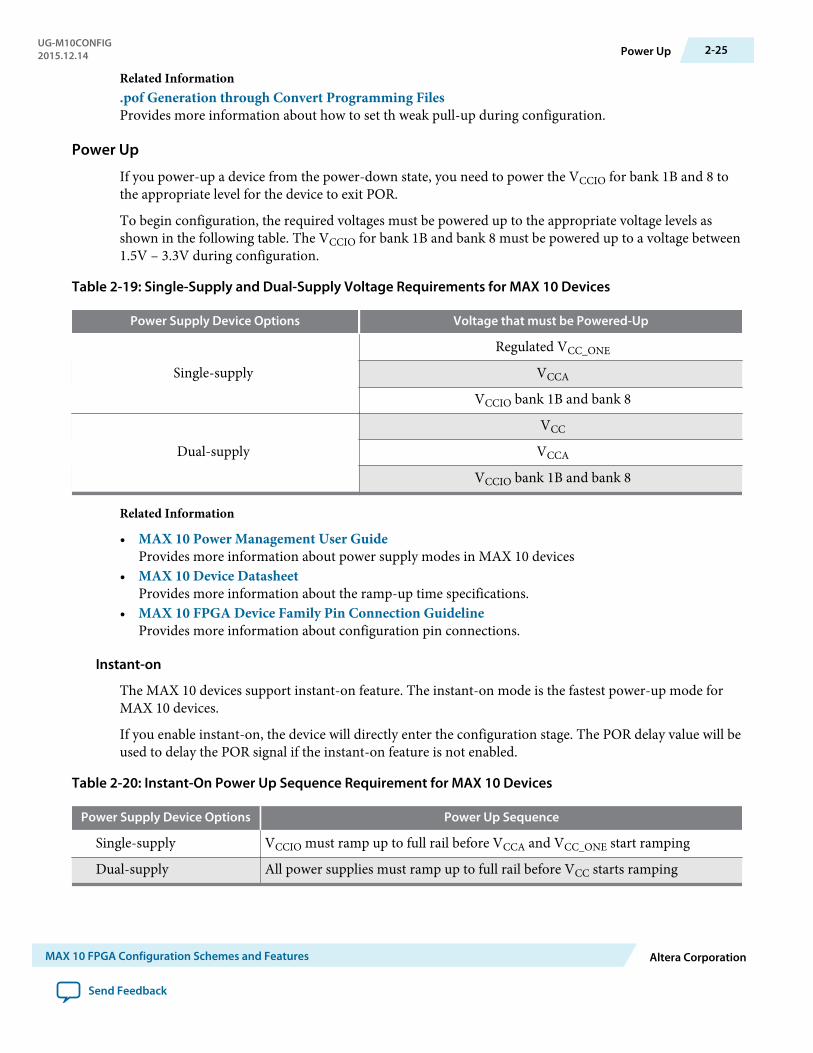
Table 2-19: Single-Supply and Dual-Supply Voltage Requirements for MAX 10 Devices
Power Supply Device Options Voltage that must be Powered-Up
Single-supply
Regulated VCC_ONE
VCCA
VCCIO bank 1B and bank 8
Dual-supply
VCC
VCCA
VCCIO bank 1B and bank 8
Related Information
• MAX 10 Power Management User GuideProvides more information about power supply modes in MAX 10 devices
• MAX 10 Device DatasheetProvides more information about the ramp-up time specifications.
• MAX 10 FPGA Device Family Pin Connection GuidelineProvides more information about configuration pin connections.
Instant-on
The MAX 10 devices support instant-on feature. The instant-on mode is the fastest power-up mode forMAX 10 devices.
If you enable instant-on, the device will directly enter the configuration stage. The POR delay value will beused to delay the POR signal if the instant-on feature is not enabled.
Table 2-20: Instant-On Power Up Sequence Requirement for MAX 10 Devices
Power Supply Device Options Power Up Sequence
Single-supply VCCIO must ramp up to full rail before VCCA and VCC_ONE start ramping
Dual-supply All power supplies must ramp up to full rail before VCC starts ramping
UG-M10CONFIG2015.12.14 Power Up 2-25
MAX 10 FPGA Configuration Schemes and Features Altera Corporation
Send Feedback

Table 2-21: POR Requirements and Timing for MAX 10 Devices
Instant-On POR Delay Setting Ramp Rate Requirement (tRAMP) POR Delay (tPOR)
Enabled Don’t Care 200 us to 3 ms No delay
Disabled Fast POR 200 us to 3 ms 3 ms to 9 ms
Disabled Standard POR 200 us to 50 ms 50 ms to 200 ms
Reset
POR delay is the time frame between the time when all the power supplies monitored by the PORcircuitry reach the recommended operating voltage and when nSTATUS is released high and the MAX 10device is ready to begin configuration.
Configuration
During configuration, the configuration data is written to the device.
Configuration Error Handling
To restart configuration automatically, turn on the Auto-restart configuration after error option in theGeneral page of the Device and Pin Options dialog box in the Quartus Prime software.
If you do not turn on this option, you can monitor the nSTATUS pin to detect errors. To restart configura‐tion, pull the nCONFIG pin low for at least the duration of tCFG.
Initialization
After you pull the CONF_DONE pin high, the initialization sequence begins. The initialization clock source isfrom the internal oscillator. By default, the internal oscillator is the clock source for initialization. If youuse the internal oscillator, the MAX 10 device will receive enough clock cycles for proper initialization.
User Mode
After the initialization completes, your design starts executing. The user I/O pins will then function asspecified by your design.
MAX 10 Configuration PinsAll configuration pins and JTAG pins in MAX 10 devices are dual-purpose pins. The configuration pinsfunction as configuration pins prior to user mode. When the device is in user mode, they function as userI/O pins or remain as configuration pins.
Table 2-22: Configuration Pin Summary for MAX 10 Devices
All pins are powered by VCCIO Bank 1B and 8.Configuration Pin Input/Output Configuration Scheme
CRC_ERROR Output only, open-drain Optional, JTAG and internal configurations
CONFIG_SEL Input only Internal configuration
DEV_CLRn Input only Optional, JTAG and internal configurations
2-26 ResetUG-M10CONFIG
2015.12.14
Altera Corporation MAX 10 FPGA Configuration Schemes and Features
Send Feedback

Configuration Pin Input/Output Configuration Scheme
DEV_OE Input only Optional, JTAG and internal configurations
CONF_DONE Bidirectional, open-drain JTAG and internal configurations
nCONFIG Input only JTAG and internal configurations
nSTATUS Bidirectional, open-drain JTAG and internal configurations
JTAGEN Input only Optional, JTAG configuration
TCK Input only JTAG configuration
TDO Output only JTAG configuration
TMS Input only JTAG configuration
TDI Input only JTAG configuration
Related Information
• Guidelines: Dual-Purpose Configuration Pin on page 3-1• Enabling Dual-purpose Pin on page 3-2
JTAG Pin Sharing Behavior
Table 2-23: JTAG Pin Sharing Behavior for MAX 10 Devices
Configuration Stage JTAG Pin Sharing JTAGEN Pin JTAG Pins (TDO, TDI, TCK, TMS)
User mode
Disabled User I/O pin Dedicated JTAG pins.
EnabledDriven low User I/O pins.
Driven high Dedicated JTAG pins.
Configuration Don’t Care Not used Dedicated JTAG pins.
UG-M10CONFIG2015.12.14 JTAG Pin Sharing Behavior 2-27
MAX 10 FPGA Configuration Schemes and Features Altera Corporation
Send Feedback

MAX 10 FPGA Configuration Design Guidelines 32015.12.14
UG-M10CONFIG Subscribe Send Feedback
Dual-Purpose Configuration Pins
Guidelines: Dual-Purpose Configuration PinTo use configuration pins as user I/O pins in user mode, you have to adhere to the following guidelines.
Table 3-1: Dual-Purpose Configuration Pin Guidelines for MAX 10 Devices
Pins Guidelines
nCONFIG During initialization:
• Tri-state the external I/O driver and drive an external pull-up resistor(6) or• Use the external I/O driver to drive the pins to the state same as the external weak pull-
up resistor
nSTATUS
CONF_DONE
nSTATUS
Tri-state the external driver of the configuration pins before the tWAIT (minimum) waittime is reached. You can use these pins for configuration purpose after tWAIT (maximum).CONF_DONE
TDO
nCONFIG
You can only use the nCONFIG pin as a single-ended input pin in user mode.
If the nCONFIG is set as user I/O, you can trigger the reconfiguration by:
• Asserting RU_nCONFIG of the remote system upgrade circuitry• Issuing PULSE_NCONFIG JTAG instruction
(6) If you intend to remove the external weak pull-up resistor, Altera recommends that you remove it afterthe device enters user mode.
© 2015 Altera Corporation. All rights reserved. ALTERA, ARRIA, CYCLONE, ENPIRION, MAX, MEGACORE, NIOS, QUARTUS and STRATIX words and logos aretrademarks of Altera Corporation and registered in the U.S. Patent and Trademark Office and in other countries. All other words and logos identified astrademarks or service marks are the property of their respective holders as described at www.altera.com/common/legal.html. Altera warrants performanceof its semiconductor products to current specifications in accordance with Altera's standard warranty, but reserves the right to make changes to anyproducts and services at any time without notice. Altera assumes no responsibility or liability arising out of the application or use of any information,product, or service described herein except as expressly agreed to in writing by Altera. Altera customers are advised to obtain the latest version of devicespecifications before relying on any published information and before placing orders for products or services.
ISO9001:2008Registered
www.altera.com101 Innovation Drive, San Jose, CA 95134
Pins Guidelines
TDO • If you intend to switch back and forth between user I/O pins and JTAG pin functionsusing the JTAGEN pin, all JTAG pins must be assigned as single-ended I/O pins orvoltage-referenced I/O pins. Schmitt trigger input is the recommended input buffer.
• JTAG pins cannot perform as JTAG pins in user mode if you assign any of the JTAGpin as a differential I/O pin.
• You must use the JTAG pins as dedicated pins and not as user I/O pins during JTAGprogramming.
• Do not toggle JTAG pin during the initialization stage.• Put the test access port (TAP) controller in reset state and drive the TDI and TMS pins
high and TCK pin low before the initialization.
TMS
TCK
TDI
Related Information
• MAX 10 FPGA Device Family Pin Connection GuidelinesProvides more information about recommended resistor values.
• MAX 10 Configuration Pins on page 2-26• JTAG Pins on page 2-2
Enabling Dual-purpose PinTo use the configuration and JTAG pins as user I/O in user mode, you must do the following in theQuartus Prime software:
1. On the Assignments menu, click Device.2. Click Device and Pin Options.3. Select the General tab of Device and Pin Options.4. In the General Options list, do the following:
• Check the Enable JTAG pin sharing.• Uncheck the Enable nCONFIG, nSTATUS, and CONF_DONE pins.
Related Information
• MAX 10 Configuration Pins on page 2-26• JTAG Pins on page 2-2
Configuring MAX 10 Devices using JTAG ConfigurationThe Quartus Prime software generates a .sof that can used for JTAG configuration. You can directlyconfigure the MAX 10 device by using a download cable with the Quartus Prime software programmer.
Alternatively, you can use the JAM Standard Test and Programming Language (STAPL) Format File(.jam) or JAM Byte Code File (.jbc) with other third-party programmer tools.
Related InformationAN 425: Using the Command-Line Jam STAPL Solution for Device Programming
3-2 Enabling Dual-purpose PinUG-M10CONFIG
2015.12.14
Altera Corporation MAX 10 FPGA Configuration Design Guidelines
Send Feedback

JTAG Configuration SetupTo configure MAX 10 device using a download cable, connect the device as shown in the following figure.
Figure 3-1: JTAG Configuration of a Single Device Using a Download Cable
VCCIO
10 kΩ
VCCIO
10 kΩ
VCCIO
10 kΩ
nSTATUSCONF_DONEnCONFIG
MAX 10
JTAGEN
TCKTDOTMS
TDI
2468
10
13579
VCCIO
10 kΩ
VCCIO
10 kΩVCCIO
JTAGEN
1 kΩ
Download Cable(JTAG Mode)
10-Pin Male Header
To configure a device in a JTAG chain, the programming software sets the other devices to bypass mode.A device in bypass mode transfers the programming data from the TDI pin to the TDO pin through a singlebypass register. The configuration data is available on the TDO pin one clock cycle later.
The Quartus Prime software uses the CONF_DONE pin to verify the completion of the configuration processthrough the JTAG port:
• CONF_DONE pin is low—indicates that the configuration has failed.• CONF_DONE pin is high—indicates that the configuration was successful.
After the configuration data is transmitted serially using the JTAG TDI port, the TCK port is clocked toperform device initialization.
Voltage Overshoot Prevention
To prevent voltage overshoot, power up the download cable to 2.5 V when VCCIO of the JTAG pins are2.5 V to 3.3 V. Tie the TCK pin to ground. If the VCCIO of the JTAG pins are using 1.5 V or 1.8 V, thedownload cable should be powered by the same VCCIO. For single-supply device which has to power-upthe download cable within the range of 3.0 V to 3.3 V, Altera recommends you to add external resistor ordiode.
UG-M10CONFIG2015.12.14 JTAG Configuration Setup 3-3
MAX 10 FPGA Configuration Design Guidelines Altera Corporation
Send Feedback

JTAGEN
If you use the JTAGEN pin, Altera recommends the following settings:
• Once you entered user mode and JTAG pins are regular I/O pins—connect the JTAGEN pin to a weakpull-down (1 kΩ).
• Once you entered user mode and JTAG pins are dedicated pins—connect the JTAGEN pin to a weakpull-up (10 kΩ).
ICB Settings in JTAG ConfigurationThe ICB settings is loaded into the device during .pof programming of the internal configuration scheme.The .sof used during JTAG configuration does not contain ICB settings. The Quartus Prime Programmerwill make the necessary setting based on the following:
• Device without ICB settings—ICB settings cleared from the internal flash or new device• Device with ICB settings—prior ICB settings programmed using .pof
Device Without ICB Settings
For devices without ICB settings, the default value will be used. However, Quartus Prime Programmerdisables the user watchdog timer by setting the Watchdog Timer Enable bit to 0. This step is to avoid anyunwanted reconfiguration occurred due to user watchdog timeout.
If the default ICB setting is undesired, you can program the desirable ICB setting first by using .pofprogramming before doing the JTAG configuration.
Device With ICB Settings
For device with ICB settings, the settings will be preserved until the internal flash is erased. Hence, youneed to remember the previous ICB settings because JTAG configuration will follow the ICB setting andbehave accordingly.
If the prior ICB setting is undesired, you can program the desirable ICB setting first by using .pofprogramming before doing the JTAG configuration.
Related Information
• .pof and ICB Settings on page 3-5• .pof Generation through Convert Programming Files
Provides more information about setting the ICB during .pof generation using Convert ProgrammingFile.
• Instant-on on page 2-25Provides more information about Instant ON and other power on reset scheme.
• Verify Protect on page 2-18• JTAG Secure Mode on page 2-17• ISP and Real-Time ISP Instructions on page 2-6• User Watchdog Timer on page 2-15
Configuring MAX 10 Devices using Internal ConfigurationThere are three main steps for using internal configuration scheme for MAX 10 devices.
3-4 ICB Settings in JTAG ConfigurationUG-M10CONFIG
2015.12.14
Altera Corporation MAX 10 FPGA Configuration Design Guidelines
Send Feedback

• Select the internal configuration scheme• Generate the .pof with ICB settings• Program the .pof the internal flash
Related Information
• Internal Configuration Modes on page 2-2• Remote System Upgrade in Dual Compressed Images on page 2-9
Selecting Internal Configuration ModesTo select the configuration mode, follow these steps:
1. Open the Quartus Prime software and load a project using a MAX 10 device.2. On the Assignments menu, click Settings. The Settings dialog box appears.3. In the Category list, select Device. The Device page appears.4. Click Device and Pin Options.5. In the Device and Pin Options dialog box, click the Configuration tab.6. In the Configuration Scheme list, select Internal Configuration.7. In the Configuration Mode list, select 1 out of 5 configuration modes available. The 10M02 devices
has only 2 modes available.8. Turn on Generate compressed bitstreams if needed.9. Click OK.
.pof and ICB SettingsThere are two methods which the .pof will be generated and setting-up the ICB. The internalconfiguration mode you selected will determine the corresponding method.
Table 3-2: .pof Generation and ICB Setting Method for Internal Configuration Modes
Internal ConfigurationMode
.pof Generation and ICBSetting Method
Description
Single CompressedImage
Auto-generated .pof(7)• Quartus Prime will automatically generate
the .pof during project compilation• ICB can be set in Device and Pin OptionsSingle Uncompressed
Image
(7) Auto-generated .pof does not allow encryption. To enable the encryption feature in Single Compressed andSingle Uncompressed mode, use the Convert Programming Files method.
UG-M10CONFIG2015.12.14 Selecting Internal Configuration Modes 3-5
MAX 10 FPGA Configuration Design Guidelines Altera Corporation
Send Feedback

Internal ConfigurationMode
.pof Generation and ICBSetting Method
Description
Single CompressedImage with MemoryInitialization.
Convert ProgrammingFiles
• User needs to generate .pof using ConvertProgramming Files.
• ICB can be set during Convert ProgrammingFiles task.
Single UncompressedImage with MemoryInitialization
Dual CompressedImages
Auto-Generated .pof
To set the ICB for the auto-generated .pof, follow these steps:
1. On the Assignments menu, click Settings. The Settings dialog box appears.2. In the Category list, select Device. The Device page appears.3. Click Device and Pin Options.4. In the Device and Pin Options dialog box, select the Configuration from the category pane.5. Click the Device Options … button.6. The Max 10 Device Options dialog box allows you to set the following:
a. Power on Reset Scheme: Instant On, Fast POR Delay or Standard POR Delay.b. User IOs week pull up during configuration.c. Verify Protect.
7. Click OK once setting is completed.
.pof Generation through Convert Programming Files
To convert .sof files to .pof files, follow these steps:
1. On the File menu, click Convert Programming Files.2. Under Output programming file, select Programmer Object File (.pof) in the Programming file
type list.3. In the Mode list, select Internal Configuration.4. To set the ICB settings, click Option/Boot Info and the ICB setting dialog box will appear. The ICB
setting dialog box allows you to set the following:a. Power on Reset Scheme: Instant On, Fast POR Delay or Standard POR Delay.b. User IOs week pull up during configuration.c. Auto-recofigure from secondary image when initial image fails (enabled by default).
Note: When you disable this feature, the device will always load the configuration image 0 withoutsampling the physical CONFIG_SEL pin. After successfully load the configuration image 0,you can switch between configuration image using the config_sel_overwrite bit of theinput register. Refer to related information for details about Altera Dual Configuration IPcore input register.
d. Use secondary image ISP data as default setting when available.e. JTAG Secure.
3-6 Auto-Generated .pofUG-M10CONFIG
2015.12.14
Altera Corporation MAX 10 FPGA Configuration Design Guidelines
Send Feedback

Note: The JTAG Secure feature will be disabled by default in Quartus Prime. If you are interestedin using the JTAG Secure feature, contact Altera for support.
Caution: MAX 10 FPGA device would become permanently locked if user enabled JTAG securemode in the POF file and POF is encrypted with the wrong key.
f. Verify Protect.g. Allow encrypted POF only.h. Watchdog timer for dual configuration and watching value (Enabled after adding 2 .sof page with 2
design that compiled with Dual Compressed Internal Images).i. User Flash Memory settings.
5. In the File name box, specify the file name for the programming file you want to create.6. To generate a Memory Map File (.map), turn on Create Memory Map File (Auto generate
output_file.map). The .map contains the address of the CFM and UFM with the ICB setting that youset through the Option/Boot Info option.
7. To generate a Raw Programming Data (.rpd), turn on Create config data RPD (Generateoutput_file_auto.rpd).Separate Raw Programming Data (.rpd) for each configuration flash memory and user flash memory(CFM0, CFM1, UFM) section will be generated together for remote system upgrade purpose.
8. The .sof can be added through Input files to convert list and you can add up to two .sof files.For remote system upgrade purpose, you can retain the original page 0 data in the .pof, and replacespage 1 data with new .sof file. To perform this, user need to add the .pof file in page 0, then add .sofpage, then add the new .sof file to page 1.
9. After all settings are set, click Generate to generate related programming file.
Programming .pof into Internal FlashYou can use the Quartus Prime Programmer to program the .pof into the CFM through JTAG interface.The Quartus Prime Programmer also allows you to program the UFM part of the internal flash.
To program the .pof into the flash, follow these steps:
1. In the Programmer window, click Hardware Setup and select USB Blaster.2. In the Mode list, select JTAG.3. Click Auto Detect button on the left pane.4. Select the device to be programmed, and click Add File.5. Select the .pof to be programmed to the selected device.6. There are several options in programming the internal flash:
UG-M10CONFIG2015.12.14 Programming .pof into Internal Flash 3-7
MAX 10 FPGA Configuration Design Guidelines Altera Corporation
Send Feedback

• To program any of the CFM0/CFM1/CFM2 only, select the corresponding CFM in the Program/Configure column.
• To program the UFM only, select the UFM in the Program/Configure column.• To program the CFM and UFM only, select the CFM and UFM in the Program/Configure column.
Note: ICB setting is preserved in this option. However, before the programming starts, QuartusPrime Programmer will make sure the ICB setting in the device and the ICB setting in theselected .pof are the same. If the ICB settings are different, Quartus Prime Programmer willoverwrite the ICB setting.
• To program the whole internal flash including the ICB settings, select the <yourpoffile.pof> in theProgram/Configure column.
7. To enable the real-time ISP mode, turn-on the Enable real-time ISP to allow background program‐ming.
8. After all settings are set, click Start to start programming.
Error DetectionThis section covers detailed guidelines on error detection.
Verifying Error Detection FunctionalityYou can inject a soft error by changing the 32-bit CRC storage register in the CRC circuitry. Afterverifying the failure induced, you can restore the 32-bit CRC value to the correct CRC value using thesame instruction and inserting the correct value. Be sure to read out the correct value before updating itwith a known bad value.
In user mode, MAX 10 devices support the CHANGE_EDREG JTAG instruction, which allows you to write tothe 32-bit storage register. You can use .jam to automate the testing and verification process. You canonly execute this instruction when the device is in user mode. This instruction enables you to dynamicallyverify the CRC functionality in-system without having to reconfigure the device. You can then switch touse the CRC circuit to check for real errors induced by an SEU.
After the test completes, to clear the CRC error and restore the original CRC value, power cycle the deviceor follow these steps:
1. After the configuration completes, use CHANGE_EDREG JTAG instruction to shift out the correctprecomputed CRC value and load the wrong CRC value to the CRC storage register. When an error isdetected, the CRC_ERROR pin will be asserted.
2. Use CHANGE_EDREG JTAG instruction to shift in the correct precomputed CRC value. The CRC_ERRORpin is de-asserted to show that the error detection CRC circuitry is working.
Related InformationSEU Mitigation and Configuration Error Detection on page 2-19
Enabling Error DetectionThe CRC error detection feature in the Quartus Prime software generates the CRC_ERROR output to theoptional dual-purpose CRC_ERROR pin.
3-8 Error DetectionUG-M10CONFIG
2015.12.14
Altera Corporation MAX 10 FPGA Configuration Design Guidelines
Send Feedback

To enable the error detection feature using CRC, follow these steps:
1. Open the Quartus Prime software and load a project using MAX 10 device family.2. On the Assignments menu, click Settings. The Settings dialog box appears.3. In the Category list, select Device.4. Click Device and Pin Options.5. In the Device and Pin Options dialog box, click the Error Detection CRC tab.6. Turn on Enable error detection CRC.7. In the Divide error check frequency by field, enter a valid divisor.
The divisor value divides down the frequency of the configuration oscillator output clock. This outputclock is used as the clock source for the error detection process.
8. Click OK.
Related InformationSEU Mitigation and Configuration Error Detection on page 2-19
Accessing Error Detection Block Through User InterfaceThe error detection circuit stores the computed 32-bit CRC signature in a 32-bit register. The user logicfrom the core reads out this signature. The fiftyfivenm_crcblock primitive is a WYSIWYG componentused to establish the interface from the user logic to the error detection circuit. Thefiftyfivenm_crcblock primitive atom contains the input and output ports that must be included in theatom. To access the logic array,you must insert the fiftyfivenm_crcblock WYSIWYG atom into yourdesign. The recommended clock frequency of .clk port is to follow the clock frequency of EDCRC block.
Figure 3-2: Error Detection Block Diagram with Interfaces for MAX 10 Devices
Clock Divider(1 to 256 Factor)
Pre-Computed CRC(Saved in the Option Register)
CRCComputation
Error DetectionLogic
SRAMBits
CRC_ERROR(Shown in BIDIR Mode)
VCC
Logic Array
CLK
SHIFT
NLD
LDSR
C REGO
UT
CRC_
ERRO
R
Internal Chip Oscillator
UG-M10CONFIG2015.12.14 Accessing Error Detection Block Through User Interface 3-9
MAX 10 FPGA Configuration Design Guidelines Altera Corporation
Send Feedback

The following example shows how the input and output ports of a WYSIWYG atom are defined in theMAX 10 device.
fiftyfivenm_crcblock <name>( .clk(<ED_CLK clock source>), .shiftnld(<ED_SHIFTNLD source>), .ldsrc (<LDSRC source>), .crcerror(<CRCERROR_CORE out destination>), .regout(<output destination>));defparam <crcblock_name>.oscillator_divider = <internal oscillator division (1 to 256)>;
Table 3-3: Port Definitions
Port Input/ Output Definition
<crcblock_name> Input Unique identifier for the CRCblock and represents anyidentifier name that is legal forthe given description languagesuch as Verilog HDL, VHDL,AHDL. This field is required.
.clk(<clock source> Input This signal designates the clockinput of this cell. All operationsof this cell are with respect to therising edge of the clock. Whetherit is the loading of the data intothe cell or data out of the cell, italways occurs on the rising edge.This port is required.
.shiftnld (<shiftnld
source>)
Input This signal is an input into theerror detection block. Ifshiftnld=1, the data is shiftedfrom the internal shift register tothe regout at each rising edge ofclk. If shiftnld=0, the shiftregister parallel loads either thepre-calculated CRC value or theupdate register contentsdepending on the ldsrc portinput. This port is required.
3-10 Accessing Error Detection Block Through User InterfaceUG-M10CONFIG
2015.12.14
Altera Corporation MAX 10 FPGA Configuration Design Guidelines
Send Feedback

Port Input/ Output Definition
.ldsrc (<ldsrc source>) Input This signal is an input into theerror detection block. Ifldsrc=0, the pre-computed CRCregister is selected for loadinginto the 32-bit shift register atthe rising edge of clk whenshiftnld=0. Ifldsrc=1, thesignature register (result of theCRC calculation) is selected forloading into the shift register atthe rising edge of clk whenshiftnld=0. This port is ignoredwhen shiftnld=1. This port isrequired.
.crcerror (<crcerror out
destination>)
Output This signal is the output of thecell that is synchronized to theinternal oscillator of the device(100-MHz or 80-MHz internaloscillator) and not to the clkport. It asserts automaticallyhigh if the error block detectsthat a SRAM bit has flipped andthe internal CRC computationhas shown a difference withrespect to the pre-computedvalue. This signal must beconnected either to an outputpin or a bidirectional pin. If it isconnected to an output pin, youcan only monitor the CRC_ERRORpin (the core cannot access thisoutput). If the CRC_ERROR signalis used by core logic to read errordetection logic, this signal mustbe connected to a BIDIR pin. Thesignal is fed to the core indirectlyby feeding a BIDIR pin that hasits oe port connected to VCC.
.regout (<output destina-
tion>)
Output This signal is the output of theerror detection shift registersynchronized to the clk port, tobe read by core logic. It shiftsone bit at each cycle. User shouldclock the clk signal 31 cycles toread out the 32 bits of the shiftregister. The values atthe .regout port are aninversion of the actual values.
UG-M10CONFIG2015.12.14 Accessing Error Detection Block Through User Interface 3-11
MAX 10 FPGA Configuration Design Guidelines Altera Corporation
Send Feedback
Related Information
• SEU Mitigation and Configuration Error Detection on page 2-19• Error Detection Timing on page 2-21
Enabling Data CompressionWhen you enable compression, the Quartus Prime software generates configuration files with compressedconfiguration data.
A compressed configuration file is needed to use the dual configuration mode in the internal configura‐tion scheme. This compressed file reduces the storage requirements in internal flash memory, anddecreases the time needed to send the bitstream to the MAX 10 device family. There are two methods toenable compression for the MAX 10 device family bitstreams in the Quartus Prime software:
• Before design compilation—using the Compiler Settings menu.• After design compilation—using the Convert Programming Files option.
Enabling Compression Before Design CompilationTo enable compression before design compilation, follow these steps:
1. On the Assignments menu, click Device. The Settings dialog box appears.2. Click Device and Pin Options. The Device and Pin Options dialog box appears.3. Click the Configuration tab.4. Turn on Generate compressed bitstreams.5. Click OK.6. In the Settings dialog box, click OK.
Related InformationConfiguration Data Compression on page 2-23
Enabling Compression After Design CompilationTo enable compression after design compilation, follow these steps:
1. On the File menu, click Convert Programming Files.2. Under Output programming file, from the pull-down menu, select your desired file type.3. If you select the Programmer Object File (.pof), you must specify a configuration device, directly
under the file type.4. In the Input files to convert box, select SOF Data.5. Click Add File to browse to the MAX 10 device family .sof.6. In the Convert Programming Files dialog box, select the .pof you added to SOF Data and click
Properties.7. In the SOF Properties dialog box, turn on the Compression option.
Related InformationConfiguration Data Compression on page 2-23
3-12 Enabling Data CompressionUG-M10CONFIG
2015.12.14
Altera Corporation MAX 10 FPGA Configuration Design Guidelines
Send Feedback

AES EncryptionThis section covers detailed guidelines on applying AES Encryption for design security. There are twomain steps in applying design security in MAX 10 devices. First is to generate the encryption keyprogramming (.ekp) file and second is to program the .ekp file into the device.
The .ekp file has other different formats, depending on the hardware and system used for programming.There are three file formats supported by the Quartus Prime software:
• JAM Byte Code (.jbc) file• JAM™ Standard Test and Programming Language (STAPL) Format (.jam) file• Serial Vector Format (.svf) file
Only the .ekp file type generated automatically from the Quartus Prime software. You must createthe .jbc, .jam and .svf files using the Quartus Prime software if these files are required in the key program‐ming.
Note: Altera recommends that you keep the .ekp file confidential.
Generating .ekp File and Encrypt Configuration FileTo generate the .ekp file and encrypt your configuration file, follow these steps:
1. On the File menu, click Convert Programming Files.2. Under Output programming file, select Programmer Object File (.pof) in the Programming file
type list.3. In the Mode list, select Internal Configuration.4. Click Option/Boot Info and the ICB setting dialog box will appear.5. You can enable the enable the Allow encrypted POF only option. Click OK once ICB setting is set.
The device will only accept encrypted bitstream during internal configuration if this option is enabled.If you encrypt one of CFM0, CFM1 or CFM2 only, the Programmer will post a warning.
6. Type the file name in the File name field, or browse to and select the file.7. Under the Input files to convert section, click SOF Data.8. Click Add File to open the Select Input File dialog box.9. Browse to the unencrypted .sof and click Open.10.Under the Input files to convert section, click on the added .sof.11.Click Properties and the SOF Files Properties: Bitstream Encryption dialog box will appear.12.Turn on Generate encrypted bitstream.13.Turn on Generate key programming file and type the .ekp file path and file name in the text area, or
browse to and select <filename>.ekp.14.You can the key with either a .key file or entering the key manually.
Note: MAX 10 devices require the entry of 128-bit keys.
UG-M10CONFIG2015.12.14 AES Encryption 3-13
MAX 10 FPGA Configuration Design Guidelines Altera Corporation
Send Feedback

• Adding key with a .key file.
The .key file is a plain text file in which each line represents a key unless the line starts with "#". The"#" symbol is used to denote comments. Each valid key line has the following format:
<key identity><white space><128-bit hexadecimal key># This is an example key filekey1 0123456789ABCDEF0123456789ABCDEF
1. Enable the Use key file checkbox.2. Click Open and add the desired .key file and click Open again.3. Under Key entry part, the key contained in the .key file will be selected in the drop-down list.4. Click OK.
• Entering you key manually.
1. Under Key entry part, click the Add button.2. Select the Key Entry Method to enter the encryption key either with the On-screen Keypad or
Keyboard.3. Enter a key name in the Key Name (alphanumeric) field.4. Key in the desired key in the Key (128-bit hexadecimal) field and repeat in the Confirm Key
field below it.5. Click OK.
15.Read the design security feature disclaimer. If you agree, turn on the acknowledgment box and clickOK.
16.In the Convert Programming Files dialog box, click OK. The <filename>.ekp and encrypted configura‐tion file will be generated in the same project directory.
Note: For dual configuration .pof file, both .sof file need to be encrypted with the same key.Thegeneration of key file and encrypted configuration file will not be successful if different keys areused.
Generating .jam/.jbc/.svf file from .ekp fileTo generate .jam/.jbc/.svf file from .ekp file, follow these steps:
1. On the Tools menu, click Programmer and the Programmer dialog box will appear.2. In the Mode list, select JTAG as the programming mode.3. Click Hardware Setup. The Hardware Setup dialog box will appear.4. Select USBBlaster as the programming hardware in the currently selected hardware list and click
Done.5. Click Add File and the Select Programmer File dialog box will appear.6. Type <filename>.ekp in the File name field and click Open.7. Select the .ekp file you added and click Program/Configure.8. On the File menu, point to Create/Update and click Create JAM, SVF, or ISC File. The Create JAM,
SVF, or ISC File dialog box will appear.9. Select the file format required for the .ekp file in the File format field.
3-14 Generating .jam/.jbc/.svf file from .ekp fileUG-M10CONFIG
2015.12.14
Altera Corporation MAX 10 FPGA Configuration Design Guidelines
Send Feedback

• JEDEC STAPL Format (.jam)• Jam STAPL Byte Code (.jbc)• Serial Vector Format (.svf)
10.Type the file name in the File name field, or browse to and select the file.11.Click OK to generate the .jam, .jbc or .svf file.
Programming .ekp File and Encrypted POF FileThere are two methods to program the encrypted .pof and .ekp file:
• Program the .ekp and .pof separately.• Integrate the .ekp into .pof and program both altogether.
Programming .ekp File and Encrypted .pof Separately
To program the .ekp and encrypted .pof separately using the Quartus Prime software, follow these steps:
1. In the Quartus Prime Programmer, under the Mode list, select JTAG as the programming mode.2. Click Hardware Setup and the Hardware Setup dialog box will appear.3. Select USBBlaster as the programming hardware in the Currently selected hardware list and click
Done.4. Click Add File and the Select Programmer File dialog box will appear.5. Type <filename>.ekp in the File name field and click Open.6. Select the .ekp file you added and click Program/Configure.7. Click Start to program the key.
Note: The Quartus Prime software message window provides information about the success or failureof the key programming operation. Once the .ekp is programmed, .pof can be programmedseparately. To retain the security key in the internal flash that had been programmed throughthe .ekp, continue with the following steps.
8. Select the .ekp to be programmed to the selected device.9. Check only the functional block that need to be updated at child level. Do not check operation at the
parent level when using Programmer GUI.10.After all settings are set, click Start to start programming.
Integrate the .ekp into .pof Programming
To integrate the .ekp into .pof and program both altogether using the Quartus Prime software, follow thesesteps:
1. In the Quartus Prime Programmer, under the Mode list, select JTAG as the programming mode.2. Click Hardware Setup and the Hardware Setup dialog box will appear.3. Select USBBlaster as the programming hardware in the Currently selected hardware list and click
Done.4. Click the Auto Detect button on the left pane.5. Select the .pof you wish to program to the device.6. Select the <yourpoffile.pof>, right click and select Add EKP File to integrate .ekp file with the .pof
file.
UG-M10CONFIG2015.12.14 Programming .ekp File and Encrypted POF File 3-15
MAX 10 FPGA Configuration Design Guidelines Altera Corporation
Send Feedback

Once the .ekp is integrated into the .pof, you can to save the integrated .pof into a new .pof. This newlysaved file will have original .pof integrated with .ekp information.
7. Select the <yourpoffile.pof> in the Program/Configure column.8. After all settings are set, click Start to start programming
Encryption in Internal ConfigurationDuring internal configuration, the FPGA decrypts the .pof with the stored key and uses the decrypted datato configure itself. The configuration image loaded during configuration is also affected by the encryptionsettings and the Auto-reconfigure from secondary image when initial image fails setting.
Table 3-4: Configuration Image Outcome Based on Encryption Settings, Encryption Key and CONFIG_SELPin Settings
Table shows the scenario when Auto-reconfigure from secondary image when initial image fails is enabled.Configura‐tion Image
Mode
CFM0 (image 0)Encryption Key
CFM1 (image 1)Encryption Key
Key Storedin the Device
AllowEncryptedPOF Only
CONFIG_SELpin
Design LoadedAfter Power-up
Single Not Encrypted Not Available No key Disabled 0 image 0Single Not Encrypted Not Available No key Disabled 1 image 0Single Not Encrypted Not Available Key X Disabled 0 image 0Single Not Encrypted Not Available Key X Disabled 1 image 0Single Not Encrypted Not Available Key X Enabled 0 Configuration FailSingle Not Encrypted Not Available Key X Enabled 1 Configuration FailSingle Key X Not Available No key Enabled 0 Configuration FailSingle Key X Not Available No key Enabled 1 Configuration FailSingle Key X Not Available Key X Enabled 0 image 0Single Key X Not Available Key X Enabled 1 image 0Single Key X Not Available Key Y Enabled 0 Configuration FailSingle Key X Not Available Key Y Enabled 1 Configuration FailDual Not Encrypted Not Encrypted No key Disabled 0 image 0Dual Not Encrypted Not Encrypted No key Disabled 1 image 1Dual Key X Not Encrypted No key Disabled 0 image 1(8)
Dual Key X Not Encrypted No key Disabled 1 image 1Dual Key X Not Encrypted Key X Disabled 0 image 0Dual Key X Not Encrypted Key X Disabled 1 image 1Dual Key X Not Encrypted Key X Enabled 0 image 0Dual Key X Not Encrypted Key X Enabled 1 image 0
(8) After image 0 configuration failed, device will automatically load image 1.(9) After image 1 configuration failed, device will automatically load image 0.
3-16 Encryption in Internal ConfigurationUG-M10CONFIG
2015.12.14
Altera Corporation MAX 10 FPGA Configuration Design Guidelines
Send Feedback

Configura‐tion Image
Mode
CFM0 (image 0)Encryption Key
CFM1 (image 1)Encryption Key
Key Storedin the Device
AllowEncryptedPOF Only
CONFIG_SELpin
Design LoadedAfter Power-up
Dual Key X Not Encrypted Key Y Enabled 0 Configuration FailDual Key X Not Encrypted Key Y Enabled 1 Configuration FailDual Key X Key X No key Enabled 0 Configuration FailDual Key X Key X No key Enabled 1 Configuration FailDual Key X Key X Key X Enabled 0 image 0Dual Key X Key X Key X Enabled 1 image 1Dual Key X Key Y Key X Enabled 0 image 0(9)
Dual Key X Key Y Key X Enabled 1 image 0Dual Key Y Key Y Key Y Enabled 0 image 0Dual Key Y Key Y Key Y Enabled 1 image 1(9)
Dual Key X Key Y Key Y Enabled 0 image 1Dual Key X Key Y Key Y Enabled 1 image 1
Table 3-5: Configuration Image Outcome Based on Encryption Settings and Encryption Key
Table shows the scenario when Auto-reconfigure from secondary image when initial image fails is disabled. Ifthis setting is disabled, device will always load image 0.
CFM0 (image 0)Encryption Key
Key Stored in theDevice
Allow Encrypted POFOnly
Design Loaded After Power-up
Not Encrypted No key Disabled image 0Not Encrypted Key X Disabled image 0Not Encrypted Key Y Disabled image 0Not Encrypted No key Enabled Configuration FailNot Encrypted Key X Enabled Configuration FailNot Encrypted Key Y Enabled Configuration FailKey X No key Disabled Configuration FailKey X Key X Disabled image 0Key X Key Y Disabled Configuration FailKey X No key Enabled Configuration FailKey X Key X Enabled image 0Key X Key Y Enabled Configuration FailKey Y No key Disabled Configuration FailKey Y Key X Disabled Configuration FailKey Y Key Y Disabled image 0l
UG-M10CONFIG2015.12.14 Encryption in Internal Configuration 3-17
MAX 10 FPGA Configuration Design Guidelines Altera Corporation
Send Feedback

CFM0 (image 0)Encryption Key
Key Stored in theDevice
Allow Encrypted POFOnly
Design Loaded After Power-up
Key Y No key Enabled Configuration FailKey Y Key X Enabled Configuration FailKey Y Key Y Enabled image 0
3-18 Encryption in Internal ConfigurationUG-M10CONFIG
2015.12.14
Altera Corporation MAX 10 FPGA Configuration Design Guidelines
Send Feedback
MAX 10 FPGA Configuration IP CoreImplementation Guides 4
2015.12.14
UG-M10CONFIG Subscribe Send Feedback
Related Information
• Introduction to Altera IP CoresProvides general information about all Altera IP cores, including parameterizing, generating,upgrading, and simulating IP.
• Creating Version-Independent IP and Qsys Simulation ScriptsCreate simulation scripts that do not require manual updates for software or IP version upgrades.
• Project Management Best PracticesGuidelines for efficient management and portability of your project and IP files.
Altera Unique Chip ID IP CoreThis section provides the guideline to implement the Altera Unique Chip ID IP Core.
Related Information
• Unique Chip ID on page 2-17• Altera Unique Chip ID IP Core Ports on page 6-1
Instantiating the Altera Unique Chip ID IP CoreTo instantiate the Altera Unique Chip ID IP Core, follow these steps:
1. On the Tools menu of the Quartus Prime software, click IP Catalog.2. Under the Library category, expand the Basic Functions and Configuration Programming.3. Select Altera Unique Chip ID and click Add, and enter your desired output file name4. In the Save IP Variation dialog box:
• Set your IP variation filename and directory.• Select IP variation file type.
5. Click Finish.
Resetting the Altera Unique Chip ID IP Core
To reset the Altera Unique Chip ID IP core, you must assert high to the reset signal for at least one clockcycle. After you de-assert the reset signal, the Altera Unique Chip ID IP core re-reads the unique chip ID
© 2015 Altera Corporation. All rights reserved. ALTERA, ARRIA, CYCLONE, ENPIRION, MAX, MEGACORE, NIOS, QUARTUS and STRATIX words and logos aretrademarks of Altera Corporation and registered in the U.S. Patent and Trademark Office and in other countries. All other words and logos identified astrademarks or service marks are the property of their respective holders as described at www.altera.com/common/legal.html. Altera warrants performanceof its semiconductor products to current specifications in accordance with Altera's standard warranty, but reserves the right to make changes to anyproducts and services at any time without notice. Altera assumes no responsibility or liability arising out of the application or use of any information,product, or service described herein except as expressly agreed to in writing by Altera. Altera customers are advised to obtain the latest version of devicespecifications before relying on any published information and before placing orders for products or services.
ISO9001:2008Registered
www.altera.com101 Innovation Drive, San Jose, CA 95134

of your device from the fuse ID block. The Altera Unique Chip ID IP core asserts the data_valid signalafter completing the operation.
Altera Dual Configuration IP CoreThis section provides the guideline to implement the Altera Dual Configuration IP Core.
Instantiating the Altera Dual Configuration IP CoreTo instantiate the Altera Dual Configuration IP Core, follow these steps:
1. On the Tools menu of the Quartus Prime software, click IP Catalog.2. Under the Library category, expand the Basic Functions and Configuration Programming.3. Select Altera Dual Configuration and after clicking Add, the IP Parameter Editor appears.4. In the New IP Instance dialog box:
• Set the top-level name of your IP.• Select the Device family.• Select the Device
5. Click OK.
4-2 Altera Dual Configuration IP CoreUG-M10CONFIG
2015.12.14
Altera Corporation MAX 10 FPGA Configuration IP Core Implementation Guides
Send Feedback
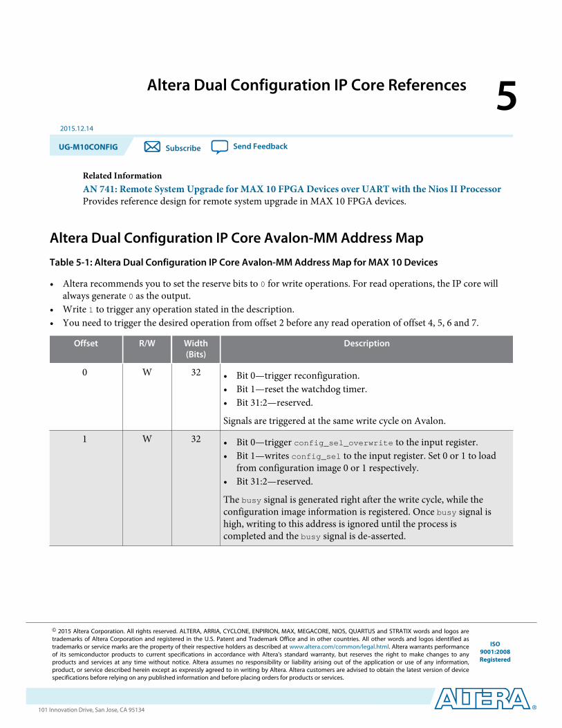
Altera Dual Configuration IP Core References 52015.12.14
UG-M10CONFIG Subscribe Send Feedback
Related InformationAN 741: Remote System Upgrade for MAX 10 FPGA Devices over UART with the Nios II ProcessorProvides reference design for remote system upgrade in MAX 10 FPGA devices.
Altera Dual Configuration IP Core Avalon-MM Address Map
Table 5-1: Altera Dual Configuration IP Core Avalon-MM Address Map for MAX 10 Devices
• Altera recommends you to set the reserve bits to 0 for write operations. For read operations, the IP core willalways generate 0 as the output.
• Write 1 to trigger any operation stated in the description.• You need to trigger the desired operation from offset 2 before any read operation of offset 4, 5, 6 and 7.
Offset R/W Width(Bits)
Description
0 W 32 • Bit 0—trigger reconfiguration.• Bit 1—reset the watchdog timer.• Bit 31:2—reserved.
Signals are triggered at the same write cycle on Avalon.
1 W 32 • Bit 0—trigger config_sel_overwrite to the input register.• Bit 1—writes config_sel to the input register. Set 0 or 1 to load
from configuration image 0 or 1 respectively.• Bit 31:2—reserved.
The busy signal is generated right after the write cycle, while theconfiguration image information is registered. Once busy signal ishigh, writing to this address is ignored until the process iscompleted and the busy signal is de-asserted.
© 2015 Altera Corporation. All rights reserved. ALTERA, ARRIA, CYCLONE, ENPIRION, MAX, MEGACORE, NIOS, QUARTUS and STRATIX words and logos aretrademarks of Altera Corporation and registered in the U.S. Patent and Trademark Office and in other countries. All other words and logos identified astrademarks or service marks are the property of their respective holders as described at www.altera.com/common/legal.html. Altera warrants performanceof its semiconductor products to current specifications in accordance with Altera's standard warranty, but reserves the right to make changes to anyproducts and services at any time without notice. Altera assumes no responsibility or liability arising out of the application or use of any information,product, or service described herein except as expressly agreed to in writing by Altera. Altera customers are advised to obtain the latest version of devicespecifications before relying on any published information and before placing orders for products or services.
ISO9001:2008Registered
www.altera.com101 Innovation Drive, San Jose, CA 95134

Offset R/W Width(Bits)
Description
2 W 32 • Bit 0—trigger read operation from the user watchdog.• Bit 1—trigger read operation from the previous state applica‐
tion 2 register.• Bit 2—trigger read operation from the previous state applica‐
tion 1 register.• Bit 3—trigger read operation from the input register.• Bit 31:4—reserved.
The busy signal is generated right after the write cycle.
3 R 32 • Bit 0—IP busy signal.• Bit 31:1—reserved.
The busy signal indicates the Dual Configuration IP core is in thewriting or reading process. In this state, all write operation to theremote system upgrade block registers operation request areignored except for triggering the reset timer. Altera recommendsyou to pull this busy signal once you triggered any read or writeprocess.
4 R 32 • Bit 11:0—user watchdog value.(10)
• Bit 12—current state of the user watchdog.• Bit 16:13—msm_cs value of the current state.• Bit 31:17—reserved.
5 R 32 • Bit 3:0—previous state application 1 reconfiguration sourcevalue from the Remote System Upgrade Status Register—Previous StateBit for MAX 10 Devices table.
• Bit 7:4—msm_cs value of the previous state application 1.• Bit 31:8—reserved.
6 R 32 • Bit 3:0—previous state application 2 reconfiguration sourcevalue from the Remote System Upgrade Status Register—Previous StateBit for MAX 10 Devices table.
• Bit 7:4—msm_cs value of the previous state application 2.• Bit 31:8—reserved.
7 R 32 • Bit 0—config_sel_overwrite value from the input register.• Bit 1—config_sel value of the input register.(11)
• Bit 31:2—reserved.
(10) You can only read the 12 most significant bit of the 29 bit user watchdog value using Dual ConfigurationIP Core.
(11) Reads the config_sel of the input register only. It will not reflect the physical CONFIG_SEL pin setting.
5-2 Altera Dual Configuration IP Core Avalon-MM Address MapUG-M10CONFIG
2015.12.14
Altera Corporation Altera Dual Configuration IP Core References
Send Feedback

Related Information
• Altera Dual Configuration IP Core on page 2-15• Avalon Interface Specifications
Provides more information about the Avalon-MM interface specifications applied in Altera DualConfiguration IP Core.
• Instantiating the Altera Dual Configuration IP Core on page 4-2• Accessing the Remote System Upgrade Block Through User Interface• Remote System Upgrade Status Registers on page 2-14
The Remote System Upgrade Status Register—Previous StateBit for MAX 10 Devices table providesmore information about previous state applications reconfiguration sources.
Altera Dual Configuration IP Core ParametersTable 5-2: Altera Dual Configuration IP Core Parameter for MAX 10
Parameter Value Description
Clock frequency Up to 80MHz Specifies the number of cycle to assert RU_nRSTIMER and RU_nCONFIG signals. Note that maximum RU_CLK is 40Mhz, AlteraDual Configuration IP Core has restriction to run at 80Mhzmaximum, which is twice faster than hardware limitation. This isbecause Altera Dual Configuration IP Core generate RU_CLK athalf rate of the input frequency.
UG-M10CONFIG2015.12.14 Altera Dual Configuration IP Core Parameters 5-3
Altera Dual Configuration IP Core References Altera Corporation
Send Feedback

Altera Unique Chip ID IP Core References 62015.12.14
UG-M10CONFIG Subscribe Send Feedback
Altera Unique Chip ID IP Core Ports
Table 6-1: Altera Unique Chip ID IP Core Ports
Port Input/Output Width (Bits) Description
clkin Input 1 • Feeds clock signal to the unique chip IDblock. The maximum supported frequencyis 100 MHz.
• When you provide a clock signal, the IP corereads the value of the unique chip ID andsends the value to the chip_id output port.
reset Input 1 • Resets the IP core when you assert the resetsignal to high for at least one clock cycle.
• The chip_id [63:0]output port holds thevalue of the unique chip ID until youreconfigure the device or reset the IP core.
data_valid Output 1 • Indicates that the unique chip ID is readyfor retrieval. If the signal is low, the IP coreis in initial state or in progress to load datafrom a fuse ID.
• After the IP core asserts the signal, the datais ready for retrieval at the chip_id[63..0]output port.
chip_id Output 64 • Indicates the unique chip ID according to itsrespective fuse ID location. The data is onlyvalid after the IP core asserts the data_valid signal.
• The value at power-up resets to 0.
© 2015 Altera Corporation. All rights reserved. ALTERA, ARRIA, CYCLONE, ENPIRION, MAX, MEGACORE, NIOS, QUARTUS and STRATIX words and logos aretrademarks of Altera Corporation and registered in the U.S. Patent and Trademark Office and in other countries. All other words and logos identified astrademarks or service marks are the property of their respective holders as described at www.altera.com/common/legal.html. Altera warrants performanceof its semiconductor products to current specifications in accordance with Altera's standard warranty, but reserves the right to make changes to anyproducts and services at any time without notice. Altera assumes no responsibility or liability arising out of the application or use of any information,product, or service described herein except as expressly agreed to in writing by Altera. Altera customers are advised to obtain the latest version of devicespecifications before relying on any published information and before placing orders for products or services.
ISO9001:2008Registered
www.altera.com101 Innovation Drive, San Jose, CA 95134

Additional Information for MAX 10 FPGAConfiguration User Guide A
2015.12.14
UG-M10CONFIG Subscribe Send Feedback
Document Revision History for MAX 10 FPGA Configuration User GuideDate Version Changes
December 2015.12.14 • Updated ICB setting description for Set I/O to weak pull-up priorusermode option to state the weak pull-up is enabled duringconfiguration.
• Removed Accessing the Remote System Upgrade Block Through UserInterface.
• Added input and output port definition for error detectionWYSIWYG atom.
• Updated the I/O pin state to be dependent on ICB bit settingduring reconfiguration.
© 2015 Altera Corporation. All rights reserved. ALTERA, ARRIA, CYCLONE, ENPIRION, MAX, MEGACORE, NIOS, QUARTUS and STRATIX words and logos aretrademarks of Altera Corporation and registered in the U.S. Patent and Trademark Office and in other countries. All other words and logos identified astrademarks or service marks are the property of their respective holders as described at www.altera.com/common/legal.html. Altera warrants performanceof its semiconductor products to current specifications in accordance with Altera's standard warranty, but reserves the right to make changes to anyproducts and services at any time without notice. Altera assumes no responsibility or liability arising out of the application or use of any information,product, or service described herein except as expressly agreed to in writing by Altera. Altera customers are advised to obtain the latest version of devicespecifications before relying on any published information and before placing orders for products or services.
ISO9001:2008Registered
www.altera.com101 Innovation Drive, San Jose, CA 95134

Date Version Changes
November 2015 2015.11.02 • Removed JRunner support for JTAG configuration and link to AN414.
• Updated differences in supported internal configuration modesupported based on device feature options in a table.
• Removed maximum number of compressed configuration imagetable do to redundancy.
• Updated Initialization Configuration Bits setting and description toreflect Quartus Prime 15.1 update.
• Updated Enable JTAG pin sharing and Enable nCONFIG,nSTATUS, and CONF_DONE pins to reflect Quartus II 15.1update.
• Added information about ISP clamp feature.• Updated information about steps to generate Raw Programming
Data (.rpd).• Renamed section title from Configuration Total Flash Memory
Programming Time to Configuration Flash Memory ProgrammingTime.
• Renamed table title from Configuration Total Flash MemoryProgramming Time for Sectors in MAX 10 Devices to ConfigurationFlash Memory Programming Time for Sectors in MAX 10 Devices.
• Added note to Configuration Flash Memory Programming Time forSectors in MAX 10 Devices table.
June 2015 2015.06.15 • Added related information link to AN 741: Remote SystemUpgrade for MAX 10 FPGA Devices over UART with the Nios IIProcessor inAltera Dual Configuration IP Core References andRemote System Upgrade in Dual Compressed Images.
• Added pulse holding requirement time for RU_nRSTIMER in RemoteSystem Upgrade Circuitry Signals for MAX 10 Devices table.
• Added link to Remote System Upgrade Status Register—PreviousState Bit for MAX 10 Devices table for related entries in Altera DualConfiguration IP Core Avalon-MM Address Map for MAX 10Devices table.
A-2 Document Revision History for MAX 10 FPGA Configuration User GuideUG-M10CONFIG
2015.12.14
Altera Corporation Additional Information for MAX 10 FPGA Configuration User Guide
Send Feedback

Date Version Changes
May 2015 2015.05.04 • Rearranged and updated Configuration Setting names 'Initializa‐tion Configuration Bits for MAX 10 Devices' table.
• Updated 'High-Level Overview of Internal Configuration for MAX10 Devices' figure with JTAG configuration and moved the figureto 'Configuration Schemes' section.
• Added link to corresponding description of configuration settingsin 'Initialization Configuration Bits for MAX 10 Devices' table.
• Updated the default watchdog time value from hexadecimal todecimal value in 'Initialization Configuration Bits for MAX 10Devices' table.
• Updated the ISP data description in 'Initialization ConfigurationBits for MAX 10 Devices' table.
• Updated 'User Watchdog Timer' by adding time-out formula.• Added link to 'User Watchdog Internal Circuitry Timing Specifica‐
tions' in MAX 10 FPGA Device Datasheet.• Added footnote to indicate that JTAG secure is disabled by default
and require Altera support to enable in 'Initialization Configura‐tion Bits for MAX 10 Devices' table.
• Updated minimum and maximum CRC calculation time fordivisor 2.
• Updated remote system upgrade flow diagram.• Updated 'Encryption in Internal Configuration' table by adding
'Key' terms and changed Image 1 and Image 2 to Image 0 andImage 1 respectively.
• Added footnote to 'Encryption in Internal Configuration' toindicate auto-reconfiguration when image fails.
• Added formula to calculate minimum and maximum CRC calcula‐tion time for other than divisor 2.
• Added caution when JTAG Secure is turned on.• Added information about auto-generated .pof for certain type of
internal configuration modes.• Added .pof and ICB setting guide through Device and Pin Options
and convert programming file.• Added configuration RAM (CRAM) in 'Overview'• Editorial changes.
December 2014 2014.12.15 • Rename BOOT_SEL pin to CONFIG_SEL pin.• Update Altera IP Core name from Dual Boot IP Core to Altera
Dual Configuration IP Core.• Added information about the AES encryption key part of ICB.• Added encryption feature guidelines.• Updated ICB settings options available in 14.1 release.• Updated Programmer options on CFM programming available in
14.1 release.
UG-M10CONFIG2015.12.14 Document Revision History for MAX 10 FPGA Configuration User Guide A-3
Additional Information for MAX 10 FPGA Configuration User Guide Altera Corporation
Send Feedback

Date Version Changes
September 2014 2014.09.22 Initial release.
A-4 Document Revision History for MAX 10 FPGA Configuration User GuideUG-M10CONFIG
2015.12.14
Altera Corporation Additional Information for MAX 10 FPGA Configuration User Guide
Send Feedback