Embed Size (px)
Citation preview

MatE/EE 167 1
EE/MatE 167
Diode Review
MatE/EE 167 2
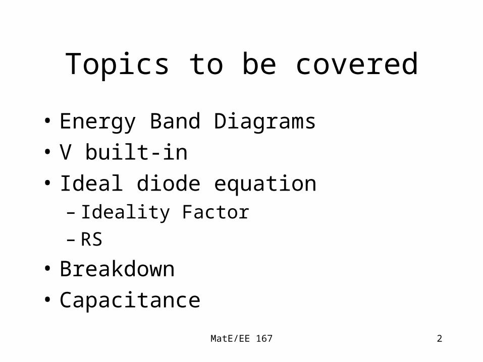
Topics to be covered
• Energy Band Diagrams
• V built-in
• Ideal diode equation– Ideality Factor– RS
• Breakdown
• Capacitance

MatE/EE 167 3

MatE/EE 167 4
Non-equilibrium conditions in a pn junction
• Equilibrium, forward bias, reverse bias
• Carrier injection
• Calculating junction current
• Minority and majority currents
• Diode equation example

MatE/EE 167 5
Equilibrium, forward bias, reverse bias
p n
Reverse B iasV r
E
Forw ard B iasV = V f
p n
E
W
p n
E
E quilibriumV =0
V p
V n
V 0
(V o-V f)
(V o+V r)

MatE/EE 167 6
Equilibrium, forward bias, reverse bias
q(V o-V f)
q(V o+V r)
E cp
E cn
E vp
E vn
E Fn
E Fp
qV o

MatE/EE 167 7
Equilibrium, forward bias, reverse bias
• Equilibrium– The Hole and electron drift and diffusion currents
cancel each other out. No net current.
• Forward bias– The junction potential is lowered by an applied
electric field.
• Reverse bias– The junction potential is increased by an applied
electric field.

MatE/EE 167 8
Equilibrium, forward bias, reverse bias
• Equilibrium– W does not change.
• Forward bias– W is smaller substitute (Vo-V) for Vo in
equation for W.
• Reverse bias– W is larger substitute (Vo+V) for Vo in
equation for W.

MatE/EE 167 9
Equilibrium, forward bias, reverse bias
• Equilibrium• EFp=EFn flat throughout .
• Forward bias• EFp(J) and EFn (J) are separated by q(Vf) (J) .
• Reverse bias• EFp(J) and EFn (J) are separated by q(Vr) (J) .

MatE/EE 167 10
Equilibrium, forward bias, reverse bias
• Equilibrium– No net current .
• Forward bias– Diffusion current is increased because the barrier is lowered and
thus more electrons and hole have enough energy to make it through the barrier. Electrons go from the n-side to the p-side. Holes go from the p-side to the n-side.
– Drift current: small because this depends on the concentration of minority carriers. Thermally generated EHP’s (within a diffusion length of W, are the only carriers that contribute to drift, thus independent of applied bias.

MatE/EE 167 11
Equilibrium, forward bias, reverse bias
• Reverse bias– Diffusion current is decreased because the barrier is higher and
thus less electrons and hole have enough energy to make it through the barrier. Electrons go from the n-side to the p-side. Holes go from the p-side to the n-side.
– Drift current: small because this depends on the concentration of minority carriers. Thermal generated EHP’s (within a diffusion length of W, are the only carriers that contribute to drift, thus independent of applied bias.

MatE/EE 167 12
Equilibrium, forward bias, reverse bias
• Equilibrium: I=I(Diff)-|I(gen)=0|
• Forward bias: I = Io(eqV/kT-1)
• Reverse bias: I=Iop n
V
I
I(gen.)
I(d if f .)
I
V
MatE/EE 167 13
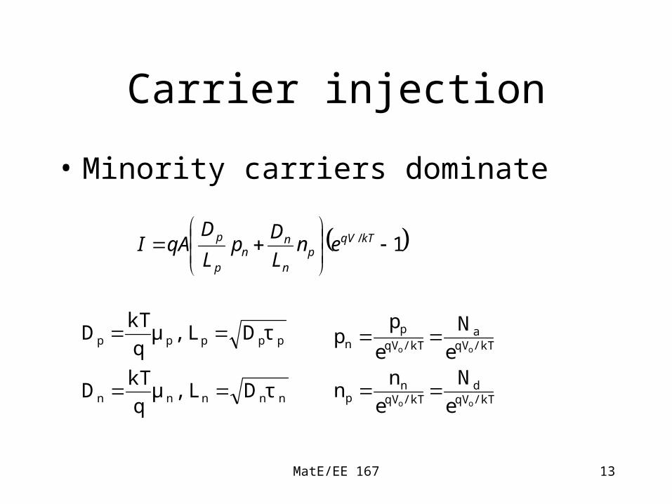
Carrier injection
• Minority carriers dominate
/kTqVd
/kTqVn
p
/kTqVa
/kTqV
pn
oo
oo
e
N
e
nn
e
N
e
pp
nnnnn
ppppp
τDL ,μq
kTD
τDL ,μq
kTD
1/
kTqV
pn
nn
p
p enL
Dp
L
DqAI

MatE/EE 167 14
Calculating junction current
• The mobilities are for electrons in p-type material, and holes in n-type material. From figure 3-23 on page 99:– An electron in p-type Si material (Na=1017cm-3)
would have a mobility of 1000 cm2/V s– A hole in n-type Ge material (Nd=1019cm-3)
would have a mobility of around 100 cm2/V s

MatE/EE 167 15
Calculating junction current
• Minority carrier lifetimes:
n
p
Si 1010-6 s 1010-6 sGe 1010-7 s 1010-7 sGaAs 110-9 s 110-9 sZnSe 110-9 s 110-9 s

MatE/EE 167 16
Minority and majority currents
)()(
)( /
npnn
Lxn
p
pnp
xIIxI
epL
qADxI pn
I
0 xn
i
)(
)(
np
nn
xI
xI
I
p+ n
x0 xn0

MatE/EE 167 17
Reverse bias breakdown
• 5.4 Reverse Breakdown (Streetman)– 5.4.1 Zener Breakdown– 5.4.2 Avalanche Breakdown

MatE/EE 167 18
Reverse bias breakdown
• Under reverse bias a pn junction exhibits a small voltage independent current until a critical voltage is reached Vbr. If the bias voltage exceeds Vbr the current increases dramatically.
• If biased properly with a current limiting diode, you can operate in reverse breakdown mode with out damaging the diode.

MatE/EE 167 19
5.4 Reverse Breakdown• 5.4.1 Zener Breakdown
– This effect applies to heavily doped junctions (p+, n+). This is a low voltage effect.
– Barrier is thin due to high abrupt doping
– When the reverse bias voltage is large enough, electrons can tunnel to the p-side, and holes can tunnel to the n-side (section 2.4.4)
– Reverse bias of a p+/n+ junction• leads to large electric field (106V/cm)
• leads to covalent electrons being “ripped away”

MatE/EE 167 20
5.4 Reverse Breakdown
• 5.4.1 Zener Breakdown
E cp
E cn
E vp
E vn
E Fn
E Fp
qV o
d
e -
I
V

MatE/EE 167 21
5.4 Reverse Breakdown
• 5.4.2 Avalanche Breakdown– Lightly doped junctions, tunneling can not
occur• W increases with reverse bias.
– Impact ionization• A carrier can be accelerated by a high electric field
with enough kinetic energy to knock an electron out of the lattices covalent bond and make an EHP. One carrier can cause many carriers to be created.
• To design Vbr, use figure 5-22 on page 190.

MatE/EE 167 22
Reverse Breakdown
• 5.4.2 Avalanche Breakdown
E
W
p n
e -
h+ e -
e -

MatE/EE 167 23
Metal Semiconductor junctions:
5.7 Metal-semiconductor junctions5.7.1 Schottky barriers
5.7.2 Rectifying contacts
5.7.3 Ohmic contacts
5.7.4 Typical Schottky barriers

MatE/EE 167 24
Schottky barriers
• Diode like behavior can be mimicked by applying clean metal to a clean semiconductor.– Easy to do and faster switching times can be realized.
• n-type– Semiconductor bands bend up causing a more positive
region near the interface, which attracts electrons from the metal to the interface interface.
• p-type– Semiconductor bands bend down causing a more
negative region near the interface, which attracts holes from the metal to the interface.

MatE/EE 167 25
Schottky barriersn-type
E cE Fs
qm qsq
M etal
Semiconductor
E FM
E v
m > s
M etal
E cE FM
E v
qbqm
E Fs
q(m sqV o
W
p-type
E c
E Fs
qm qsq
M etal
Semiconductor
E FM
E v
m < s
M etal
E c
E FM
E v
E Fs
q(s mqV o
W

MatE/EE 167 26
Rectifying contacts
• Apply a forward bias to the Metal of the M/S(n) diode and the contact potential is reduced by Vo-V
– Allows electrons to diffuse into metal.• Apply a forward bias to the Semiconductor of the
M/S(p) diode and the contact potential is reduced by Vo-V
– Allows holes to diffuse into metal.
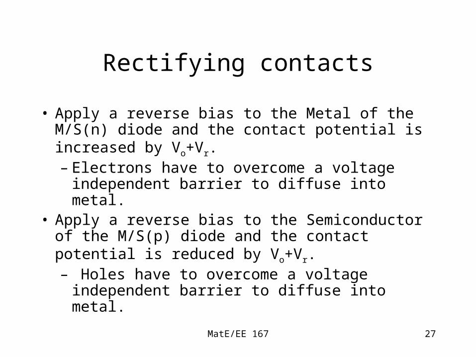
MatE/EE 167 27
Rectifying contacts
• Apply a reverse bias to the Metal of the M/S(n) diode and the contact potential is increased by Vo+Vr.– Electrons have to overcome a voltage
independent barrier to diffuse into metal.• Apply a reverse bias to the Semiconductor of the
M/S(p) diode and the contact potential is reduced by Vo+Vr.– Holes have to overcome a voltage independent
barrier to diffuse into metal.

MatE/EE 167 28
Rectifying contacts
• Current flows primarily by majority carriers is both cases.
• Very little charge storage occurs, which leads to fast switching speeds.

MatE/EE 167 29
Ohmic contacts
• Metal/semiconductor ohmic contacts– linear near the origin, non-rectifying
• Two methods of fabrication– Choose a metal with a workfunction that aligns the
fermi levels with majority carriers. (Al for p-type Si, Au for n-type Si
– Dope the semiconductor heavily so that W is very thin so that tunneling occurs (Al on p+ or n+ Si)
– Heavy doping all ways improves ohmic behavior.

MatE/EE 167 30
Ohmic contactsp-type
E c
E Fs
qm qsq
M etal
SemiconductorE FM
E v
m > s
M etal
E c
E FM
E v
E Fs
q(m sqV o
W

MatE/EE 167 31
Ohmic contactsn-type
E cE Fs
qm qsq
M etal
Semiconductor
E FM
E v
m < s
M etal
E cE FM
E v
qbqm
E Fsq(s mqV o
W

MatE/EE 167 32
Real Schottky barriers
• In Si, there is a thin oxide in between the metal and semiconductor.
• Surface states arise from the crystal ending– This can pin the fermi level to midgap in GaAs
• If a metal semiconductor junction is alloyed the interface is blurred between metal/metal-semiconductor/semiconductor.
• Contact design is very dependant on your process.

MatE/EE 167 33
Equations
2ioo npn
ppp
nnn
DL
DL
q
kTD
1enL
Dp
L
DqAI qV/nkT
pn
nn
p
p
2i
da
n
NNln
q
kTVo
2
1
2
1
)(
2
2)(
2
da
da
ooj
da
da
da
dao
NN
NN
VV
qA
VVd
dQC
WNN
NNqAQ
NN
NN
q
VVW

MatE/EE 167 34
Breakdown