Embed Size (px)
Citation preview

European Space Agency
FINAL REPORT Stage 15 March 99 –10 September 99
Microelectronics Section Control, Data & Power Division
ESTEC
MASTER / TARGET PCI
VHDL CORE
Riccardo Locatelli and Mr.Sandi Habinc
E.W.P 2047

Master/Target PCI VHDL Core
2

Master/Target PCI VHDL Core
3
Acknowledgment
I would like to thank Mr. Richard Creasey, Head of TOS-ES Division, for giving
me the opportunity to work in the Division and for providing a peaceful working
environment.
I would also like to thank Mr. Martin Hollreiser, Head of the Microelectronics
Section, and people working in TOS-ESM Section for their advice and help offered to me
during this period.
It has been a great pleasure to work under Mr. Sandi Habinc’s supervision during
six months of training at ESTEC. Microelectronics engineer of the TOS-ESM at ESTEC,
Mr. Habinc is a very professional person, competent and helpful in any situation; his
enthusiasm and knowledgeable suggestions have made my Stage at ESTEC a pleasant and
profitable one.
I would like to thank Mr. Pierangelo Terreni, Engineer and Professor at Electronic
Engineering University of Pisa, supervisor of my degree thesis in Italy, for giving me the
possibility to carry out my thesis work outside the University.
I would like to express my gratitude to Mr. Luca Fanucci, Engineer and Researcher
at CNR-CSMDR, University of Pisa, for his constant availability and kindness, for his
attentions and precious advice for the whole period of my Stage at ESTEC.
I would like to thank all friends who stood by me during this period for contributing
to make my stay in Holland a pleasant one.
Thanks to my parents for their enthusiasm, support and joy in every moment.
Special thanks to a special person.

Master/Target PCI VHDL Core
4
Table of Content 1. INTRODUCTION............................................................ 6
1.1 ORGANISATION................................................................. 6 1.2 PCI LOCAL BUS.................................................................. 7 1.3 CONVENTIONS................................................................... 8
2. OVERVIEW...................................................................... 9
2.1 GENERAL DESCRIPTION.................................................. 9 2.2 SUPPORTED PCI FEATURES............................................ 10 2.3 BUS SEQUENCER ARCHITECTURE................................ 12
3. PCI INTERFACE............................................................. 14
3.1 MASTER INTERFACE........................................................ 18 3.2 TARGET INTERFACE......................................................... 19
4. BACK-END INTERFACE.............................................. 20
4.1 LOCAL CONFIGURATION INTERFACE......................... 20 4.2 INTERNAL MASTER INTERFACE................................... 23
4.2.1 Single read........................................................................ 25 4.2.2 Burst read not-prefetchable.............................................. 26 4.2.3 Burst read prefetchable..................................................... 27 4.2.4 Single write ...................................................................... 28 4.2.5 Burst write........................................................................ 29 4.2.6 FIFO IN............................................................................ 30 4.2.7 FIFO OUT........................................................................ 32
4.3 INTERNAL TARGET INTERFACE.................................... 35 4.3.1 Memory write................................................................... 37 4.3.2 Memory Read prefetchable.............................................. 39 4.3.3 Read not-prefetchable....................................................... 40 4.3.4 I/O write............................................................................ 41 4.3.5 Configuration cycles......................................................... 42

Master/Target PCI VHDL Core
5
4.3.6 FIFO IN............................................................................ 42 4.3.7 FIFO OUT........................................................................ 44
4.4 EXTERNAL SIGNALS........................................................ 47
5. FUNCTIONAL BLOCK.................................................. 48 5.1 MASTER FUNCTIONAL DESCRIPTION.......................... 48
5.1.1 Master State Machine....................................................... 49 5.1.2 Master AD / CBE Buffers................................................ 53 5.1.3 FIFO IN Block Master...................................................... 54 5.1.4 FIFO OUT Block Master.................................................. 56 5.1.5 Master Parity & Error Block............................................ 58
5.2 TARGET FUNCTIONAL DESCRIPTION.......................... 60 5.2.1 Target State Machine........................................................ 60 5.2.2 Target AD / CBE Buffers................................................. 64 5.2.3 FIFO Block Target............................................................ 65 5.2.4 Target Parity & Error Block............................................. 66
5.3 CONFIGURATION BLOCK................................................ 68 6. VHDL CORE OVERVIEW............................................. 72
6.1 FILE NAMES........................................................................ 72 REFERENCES APPENDIX A: VHDL CODE

Master/Target PCI VHDL Core
6
1. INTRODUCTION
This report presents the activity performed by Riccardo Locatelli during a stage
period at the European Space Research and Technology Center (ESTEC) of the European
Space Agency (ESA), in the Netherlands.
The training period, from March to September 1999, was developed under the
supervision of Mr. Sandi Habinc, within the Microelectronics Section of the Control, Data
& Power Division (TOS-ESM).
The subject of the activity was the design of a Master / Target PCI Interface
following a top-down approach based on VHDL and logic synthesis.
1.1 ORGANISATION
The report is divided in the following sections:
• Chapter 2, “Overview”: it gives a general description of the PCI Core, its features and
the functional architecture.
• Chapter 3, “PCI Interface”: it describes the front-end interface, i.e. the PCI signals.
There are three different lists of signals, for the Master and the Target side and one for
the complete PCI Core.
• Chapter 4, “Back-end Interface”: this is the definition of the interface with the back-
end application, that consists of a FIFO Interface, a Local Configuration Interface and
three external signals. Timing, functional description, encoding and pictures are
provided in order to describe the interconnection with the local user.
• Chapter 5, “Functional Blocks”: it provides the complete functional and structural
architecture of each block implemented.
• Chapter 6, “VHDL Core Overview”: it presents the organization of the VHDL code.

Master/Target PCI VHDL Core
7
1.2 PCI LOCAL BUS
The PCI Local Bus is a high performance, 32-bit or 64-bit bus with multiplexed
address and data lines. This is a fully synchronous bus with operation up to 33Mhz or
66Mhz and a high bus bandwidth (132 Mbytes/second burst transfer for 32-bit data path at
33 Mhz). There is a hidden central arbitration to support the multi-master capability. Both
5-volt and 3.3-volt (mobile applications) environments are specified.
Ease of installation, dynamic configuration changes and backward compatibility
(Plug & Play) are achieved thanks to the configuration support of PCI devices.
The PCI Local Bus is an interconnect mechanism between highly integrated
peripheral controller components, add-in boards and processor/memory systems.
Typical PCI applications are add-on cards that require high-speed memory access
(LAN or graphics adapters, SCSI cards); a standard definition for the compatibility with
low bandwidth I/O buses such as ISA, EISA or MC reduces inventory cost and end user
confusion. Figure 1.1 shows an overview of a possible PCI system.
Figure 1.1 PCI System overview
Host processor
Cache memory
System memory
PCI Bus Primary Bridge
PCI Local Bus – Level 0
SCSI LAN
PCI to PCI Bridge
Motion Video
Graphics PCI to Bus X Secondary Bridge
ESA / EISA, MicroChannel
PCI Local Bus – Level 1Base I / O Functions Low
bandwidth

Master/Target PCI VHDL Core
8
1.3 CONVENTIONS - Master: an agent that initiates transactions on the PCI Bus; it drives commands on the
address phase requesting write or read accesses to one of the three address spaces of
the PCI Bus (Configuration, I/O, Memory).
- Target: it is the slave, which claims and responds to the transaction initiated on the
PCI bus by a master agent.
Figure 1.2 PCI Master/Target devices - Bus sequencer: it is the first part of the bus interface, which performs the bus
operation as requested and guarantees the PCI protocol is not violated.
- Back-end application: this is the second part of the bus interface, which represents the
local side user application.
Figure 1.3 PCI Bus Interface
MASTER
TARGET
WRITE
READ
PCI BUS
BUS SEQUENCER
BACK-END APPLICATION

Master/Target PCI VHDL Core
9
- Signals ending with “#” are active low signals
- Single transaction: PCI Bus cycle with the address phase and one data phase with one
32-bit data transfer.
- Burst transaction: PCI Bus cycle that consists of an address phase and two or more
data phase, i.e. two or more 32-bit data transfers.
2. OVERVIEW
This chapter wants to give to the reader a general description about the features and
the functional organization of the PCI Core, without describing details but providing an
overall overview.
2.1 GENERAL DESCRIPTION
The PCI Core is an ASIC VHDL implementation of 32-bit, 33 Mhz PCI Master /
Target Bus sequencer, fully compliant with the PCI Local Bus Standard, Revision 2.1.
The synthesizable VHDL code was verified by using ad-hoc developed test-
benches and optimized for MIETEC 0.35 µm CMOS technology.
The PCI Core handles single and burst Configuration, I/O and Memory cycles.
Zero-wait state burst transactions are supported for Memory and Configuration accesses,
thus achieving 132 Mbytes/second throughput, which is the maximum bandwidth for 32-
bit, 33 Mhz PCI bus.
The Master and Target devices can operate independently; the separate data paths
and an easy FIFO Interface with back-end application allow an efficient usage of the bus
by implementing independent data prefetching and posting.

Master/Target PCI VHDL Core
10
2.2 SUPPORTED PCI FEATURES
This is a list of the main features supported by the PCI Core; the full compliance with PCI Local Bus Standard (Revision 2.1) was achieved.
• 32-bit data bus • 33 Mhz (Bandwidth 132 Mbytes/sec peak) • Read and write transactions to the three different PCI address spaces:
Memory, I/O and Configuration. • Master initiated termination:
- Completion: this is the normal termination, which occurs when the master has concluded its intended transaction.
- Time-out: it refers to the expiration of the Latency Timer when the master is keeping the bus for many PCI clock periods without the grant from the arbiter. This timer wants avoid the extension of the access latency of other possible master of the Bus system.
- Master-Abort: this is the protocol for the termination when no target claims the access initiated by the master.
• Target initiated termination: - Retry: this is a particular Disconnect without any data transferred; target is not
ready for the transaction and stops it before the first data transfer. The master has to repeat this transaction later.
- Disconnect: target has claimed the access, started the data handshake; it wants to terminate the transaction before the Master Completion.
- Target-Abort: it refers to an abnormal end because the target detected a fatal error or it will never be able to complete the request; it can occur at any moment during the first or the subsequent data phases.
• Bus parking. The arbiter can select the default owner of the bus when no agent is currently using or requesting it. This master has to drive the bus lines so that it will not float.
• Exclusive access support: the Target implements the partial lock of one BAR (Base Address Register).
• Fast back-to-back cycles as Master and Target: two different accesses by the same master can occur without the turn-around clock period which is usually requested for all signals that may be driven by more than one agent.
• Parity is generated and possible errors are checked and reported to back-end application.
• Medium speed decoder as Target.

Master/Target PCI VHDL Core
11
• Latency requirements: there is a fixed number of PCI clocks within the agent has to provide the next data valid. The PCI Core has internal timers to achieve this function.
• Type zero Configuration Space; all required registers are supported. - Burst zero-wait configuration read and write cycles - Dual-access support: the Configuration Space is accessible from the PCI and the
back-end side. • Easy FIFO Interface with back-end application.
- Zero-wait prefetchable read as Master thanks to the FIFO interface where read data are stored independently of the master back-end user clock.
- Posting data as Target. The transaction completes at the source (PCI bus master) before it actually completes at the intended destination (target back-end user) because data are stored into FIFO memories.
• Special Cycle supported with internal decoding for single cycle message HALT and SHUTDOWN.
• Configuration, I/O and Memory commands implemented inclusive the Memory Read Line and Memory Read Multiple, which are treated as normal memory read. Memory Write & Invalidate has a special support (cacheline counter) for the time-out ending protocol. Table 2.1 presents a list of all possible commands, indicating which are supported by the PCI Core.
C/BE#[3::0] COMMAND TYPE SUPPORTED 0000 Interrupt Acknowledge No 0001 Special Cycle Yes 0010 I/O Read Yes 0011 I/O Write Yes 0100 Reserved --- 0101 Reserved --- 0110 Memory Read Yes 0111 Memory Write Yes 1000 Reserved --- 1001 Reserved --- 1010 Configuration Read Yes 1011 Configuration Write Yes 1100 Memory Read Multiple Yes 1101 Dual Address Cycle No 1110 Memory Read Line Yes 1111 Memory Write & Invalidate Yes
Table 2.1 PCI Commands

Master/Target PCI VHDL Core
12
2.3 BUS SEQUENCER ARCHITECTURE
The functional structure of the PCI Master/Target Bus sequencer was carried out in
a hierarchical and symmetric way in order to design a modular VHDL model very flexible
and with an ease sub-blocks re-use.
The PCI Core is both a Master and a Target; according to the suggestion of the PCI
Local Bus Standard each must have its own control machine that can operate
independently of the other to avoid conflicts.
The block diagram shown in figure 2.1 illustrates this organization. This below is a
list of the functional blocks of the PCI Core:
• Master State Machine: this block reports the sequencing of operations on the PCI bus
driving the arbitration and the interface control signals according to the PCI protocol.
• FIFO Block Master: it manages the handshake between the Master State Machine and
the back-end application handling in the right way the information to/from FIFO
Interface.
• AD/CBE Buffers Master: it connects the 32-bit multiplexed PCI address/data bus
with the two unidirectional 32-bit local address/data buses. It is also used to drive
correctly the command/byte enables lines.
• Parity&Error Master: it computes parity and reports parity errors when the PCI Core
is working as Master.
• Target State Machine: this block manages the right PCI protocol for all supported
commands driving the interface control signals when the agent becomes slave of a bus
transaction.
• FIFO Block Target: It handles the handshake between the Target State Machine and
the back-end application; this block is connected to the back-end FIFOs and
implements the posting data for memory write.
• AD/CBE Buffers Target: it connects the 32-bit address/data lines of the PCI bus with
the two internal unidirectional 32-bit local address/data buses. There are two different
data paths for the Master and the Target part of the PCI Core.
• Parity&Error Target: it computes parity and reports errors when the PCI Bus
Sequencer is working as Target.
• Configuration Space: it implements the configuration registers and handles read/write
accesses to them. It also manages the address decoding for Memory and I/O cycles.

Master/Target PCI VHDL Core
13
Figure 2.1 PCI Core Overview
MASTER STATEMACHINE
AD/CBEBUFFERSMASTER
FIFOBLOCK
MASTER
PARITY & ERRORMASTER
CONFIGURATIONBLOCK
PARITY & ERRORTARGET
AD / CBEBUFFERSTARGET
FIFOBLOCK
TARGET
TARGET STATEMACHINE

Master/Target PCI VHDL Core
14
3. PCI INTERFACE
The PCI Bus sequencer has a front-end interface, which is the direct connection to
the PCI bus and a back-end interface, which is the no-standard interface with the local
user.
The PCI Interface of a compliant device requires a minimum of 47 pins for a target-
only device and 49 pins for a master. The PCI Core implements all the required signals; the
PCI Local Bus Standard defines 51 optional pins and only one of these is a PCI Interface
signal of the PCI Core. Figure 3.1 shows the complete list of the required and optional pins
in functional groups.
Figure 3.1 PCI Pin List
PCI COMPLIANT
DEVICE
AD [31::0]
CBE [3::0]
PAR
Address & Data
FRAME IRDY DEVSEL TRDY STOP IDSEL
Interface Control
PERR SERR
Error Reporting
REQ GNT
Arbitration(Master only)
CLK RSTSystem
AD [63::32]
CBE [7::4]
PAR64
REQ64ACK64
64-bitExtension
LOCK InterfaceControl
INTAINTBINTCINTD
Interrupts
SBOSDONE
Cache Support
TDI TDOTCK
TMS TRST
JTAG (IEEE 1149.1)
Required Pins Optional Pins

Master/Target PCI VHDL Core
15
It is possible divide the PCI bus signals into five different types:
• Input, In: a standard input-only signal.
• Output, Out: a standard active output-only driver.
• Tri-State, t/s: a bi-directional, tri-state input output pin.
• Sustained Tri-State, s/t/s: an active low tri-state signal owned and driven by one
and only one agent at a time. The agent that drives a s/t/s pin low must drive it high for
at least one clock before letting it float. A new agent cannot start driving a s/t/s signal
any sooner than one clock after the previous owner tri-states it. A pull-up is required to
sustain the inactive state until another agent drives it.
• Open Drain, o/d: a wire-ORed with other agents. The signaling agent asserts the
open-drain signal, and a weak pull-up resistor de-asserts it. The pull-up resistor may
require two or three PCI clock cycles to restore the open-drain signal to its inactive
state.
• System pins
CLK is the system clock that provides, as input to every PCI device, the reference
signal for all other PCI interface signals except RST# and the interrupt pins.
RST# is the system reset. It can be asserted asynchronously to the PCI bus clock edge.
The synchronized version of this signal is used as general reset of the complete PCI Core.
• Address and Data pins
AD[31::0] is a time-multiplexed address/data bus. Each bus transaction consists of an
address phase followed by one or more data phases. The data transfer occurs when IRDY#
and TRDY# are both asserted. The first rising edge when FRAME# is asserted is the
beginning of the transaction, i.e. the address phase (address on the AD bus and command
on the C/BE lines).
C/BE#[3::0] is a multiplexed command/byte enables bus. During the address phase
these lines are carrying command and during the data phases they indicate the byte
enables.
PAR is the parity signal. It is an even parity across AD and C/BE lines. PAR must be
valid one clock following its corresponding data or address on the bus. It is calculated by
the agent that is driving the AD bus.

Master/Target PCI VHDL Core
16
• Interface Control Pins
FRAME# is the cycle frame; it is driven by the current master to indicate the
beginning and duration of an access. While it is asserted, data transfers continue; it has to
be de-asserted before the last data transfer to indicate that the next data phase is the last
one.
IRDY# indicates the master’s ability to complete the current data phase of the
transaction. It can be de-asserted by the master during the data phase to insert wait cycles;
when IRDY# and TRDY# are both asserted the data transfer occurs.
TRDY# is used by the target to indicate the ability to complete the current data phase
of the transaction. It is de-asserted to insert wait cycles.
STOP# is the signal used by the current target for requesting the master to stop the
transaction implementing the protocol of a target initiated termination.
DEVSEL# is driven by the agent which has decoded its address as the target of the
current access. It is asserted to claim the access, i.e. to accept the master request.
LOCK# is the signal used to implement the exclusive access on the PCI bus. It
indicates an atomic operation that may require multiple transactions to complete. When
LOCK# is asserted, non-exclusive transactions may proceed to an address that is not
currently locked. It is possible for different agents to use the bus while a single master
retains ownership of LOCK#. A target of an access that supports LOCK# must provide
exclusion to a minimum of 16 bytes aligned. The PCI Core as target is able to guarantee
that a BAR is locked instead of the complete resource.
IDSEL is a sort of chip select for configuration transactions. When it is asserted,
during the address phase, it means that transaction is an access to the Configuration Space.
• Arbitration Pins
REQ# is driven by the master for requesting to the arbiter the use of the bus.
GNT# indicates to the agent that access to the bus has been granted.
• Error Reporting Pins
PERR# reports possible parity errors during all PCI transaction except a Special Cycle.
It is driven by the device, that receives data, two clocks following the data itself.
SERR# is a synchronous signal but it has not timing requirements. It is for reporting
address parity errors, data parity errors on the Special Cycle and for any other system
errors where the result will be catastrophic.

Master/Target PCI VHDL Core
17
Table 3.1 summarizes the PCI bus signals that provide the interface between the
PCI Core and the PCI Bus (see also Fig. 3.2).
NAME TYPE DIRECTION ACTIVE SYNC/ASYNC CLK In Input High Sync RST# In Input Low Async AD[31::0] T/s Bi-directional High Sync C/BE#[3::0] T/s Bi-directional Low Sync PAR T/s Bi-directional High Sync FRAME# S/t/s Bi-directional Low Sync IRDY# S/t/s Bi-directional Low Sync TRDY# S/t/s Bi-directional Low Sync STOP# S/t/s Bi-directional Low Sync DEVSEL# S/t/s Bi-directional Low Sync REQ# T/s Output Low Sync GNT# T/s Input Low Sync LOCK# S/t/s Bi-directional Low Sync IDSEL In Input High Sync PERR# S/t/s Bi-directional Low Sync SERR# o/d Output Low Sync
Table 3.1 PCI Interface signals
Figure 3.2 PCI Interface of the Master/Target PCI Core
MASTER / TARGET PCI CORE
AD[31..0]
CBE[3..0]
PAR
FRAME]
IRDY
DEVSEL
TRDY
STOP
CLK
RST
REQ
GNT
PERR
SERR
IDSEL

Master/Target PCI VHDL Core
18
3.1 MASTER INTERFACE
Table 3.2 shows the list of PCI signals which are in the port description of the
Master block of the PCI Core.
NAME TYPE DIRECTION ACTIVE SYNC/ASYNC CLK In Input High Sync RST# In Input Low Async AD[31::0] t/s Bi-directional High Sync C/BE#[3::0] t/s Output Low Sync PAR t/s Bi-directional High Sync FRAME# s/t/s Bi-directional Low Sync IRDY# s/t/s Bi-directional Low Sync TRDY# s/t/s Input Low Sync STOP# s/t/s Input Low Sync DEVSEL# s/t/s Input Low Sync REQ# t/s Output Low Sync GNT# t/s Input Low Sync LOCK# s/t/s Bi-directional Low Sync PERR# s/t/s Bi-directional Low Sync
Table 3.2 Master PCI Interface signals of the PCI Core
Figure 3.3 PCI Interface of the Master Block of the PCI Core
MASTER BLOCK PCI CORE
AD[31..0]
CBE[3..0]
PAR
FRAME]
IRDY
DEVSEL
TRDY
STOP
CLK
RST
REQ
GNT
PERR

Master/Target PCI VHDL Core
19
3.2 TARGET INTERFACE
Table 3.3 shows the PCI signals that represent the front-end interface of the Target
block of the PCI Core (see also Fig. 3.4).
NAME TYPE DIRECTION ACTIVE SYNC/ASYNC CLK In Input High Sync RST# In Input Low Async AD[31::0] t/s Bi-directional High Sync C/BE#[3::0] t/s Input Low Sync PAR t/s Bi-directional High Sync FRAME# s/t/s Input Low Sync IRDY# s/t/s Input Low Sync TRDY# s/t/s Output Low Sync STOP# s/t/s Output Low Sync DEVSEL# s/t/s Output Low Sync LOCK# s/t/s Input Low Sync IDSEL In Input High Sync PERR# s/t/s Output Low Sync SERR# o/d Output Low Sync
Table 3.3 Target PCI Interface signals of the PCI Core
Figure 3.4 PCI Interface of the Target Block of the PCI Core
TARGET BLOCK PCI CORE
AD[31..0]
CBE[3..0]
PAR
FRAME]
IRDY
DEVSEL
TRDY
STOP
CLK
RST
REQ
GNT
PERR
SERR

Master/Target PCI VHDL Core
20
4. BACK-END INTERFACE
The interface of the PCI Core with the back-end application consists of an easy
FIFO Interface, a simple interface for the direct access to the Configuration Space from the
local side and three external signals.
There are four 40-bit word FIFOs; they are asynchronous, unidirectional and are
called IN (info direction Back-end => Core) and OUT (info direction Core => Back-end).
FIFO are used not only to carry data and addresses but also to provide all useful
information between the PCI Core and the back-end user to implement the bus transaction.
This is a very easy and friendly interface, which isolates the application from the
complexity of the PCI protocol and manages the data buffering and synchronizing between
the PCI side and the local user. A great flexibility is achieved thanks to this FIFO interface,
thus increasing the possibility of supporting many different kind of back-end applications.
Local application independence is not only from the point of view of back-end frequency
(slow or fast are supported) but also of its implementation architecture.
4.1 LOCAL CONFIGURATION INTERFACE
The Configuration Space has a support for handling dual-side read and write
accesses from the PCI bus and the back-end application. This interface allows the direct
access of the local user to the Configuration Space without using the PCI bus or dedicated
internal signals. Figure 4.1 describes the signals of this interface.
Figure 4.1 Local Configuration Interface
CONFIGURATION BLOCK
Req_back
Ack_back
Address_back
Data_in_back
Data_out_back
Notvalid_back
Back-end
Application

Master/Target PCI VHDL Core
21
Req_back is the request signal, which is asserted by the back-end for implementing
a write operation into the Configuration Space. The request is accepted if the PCI Core
drives active the acknowledgment signal.
Ack_back is the acknowledgment for write request coming from the back-end; the
PCI Core doesn’t assert it to avoid the possibility to write when a PCI Configuration access
is occurring to that Configuration Space.
Address_back is a 6-bit address bus; the Configuration Space consists of
256Kbytes divided into 32-bit lines.
Data_in_back is the 32-bit data bus for write operations; back-end is allowed to
write with 32-bit single accesses.
Data_out_back is the 32-bit data bus where the local user can read data. The data
path consists of two unidirectional buses and this is the easier solution for an asynchronous
interface. For reading, back-end has not to deal with a particular handshake: according to
the address in the address_back bus the right value of the corresponding 32-bit line is
presented on this bus.
Notvalid_back is asserted by the Configuration support when a PCI cycle is
occurring, thus indicating not valid data on the data out bus.
Table 4.1 summarizes signals of this interface which have just been described.
NAME TYPE DIRECTION ACTIVE SYNC/ASYNC Req_back In Input High Async Ack_back Out Output High Sync Address_back In Input High Async Data_in_back In Input High Async Data_out_back Out Output High Sync Notvalid_back Out Output High Sync
Table 4.1 Local Configuration Interface signals

Master/Target PCI VHDL Core
22
WRITE Cycle: it is a single 32-bit access with a request-acknowledgment
handshake between the PCI Core and the back-end application.
Address_back is sampled by the Configuration support each rising-edge of the PCI
clock; data write has to keep stable on the Data_in_back bus according to this timing.
Writing of the registers occurs on the second PCI clock when both Req_back and
Ack_back are asserted.
Figure 4.2 Back-end Direct Configuration Write access
READ Cycle: back-end has only to drive the Address_back bus with the right
address value and the corresponding data can be read on the Data_out_back, except when
Notvalid_back is asserted; this means that a PCI access is occurring and data read are not-
valid.
Figure 4.3 Back-end Direct Configuration Read access
ADDRESS
WRITE DATA VALID
OLD NEW
Req_back
Ack_back
Address_back
Data_in_back
Data_out_back
ADDRESS
DATA VALID
Address_back
Data_out_back
Notvalid_back

Master/Target PCI VHDL Core
23
4.2 INTERNAL MASTER INTERFACE
This internal interface connects the Master bus sequencer with the back-end
application, i.e. the master side of the local user. It is a complete FIFO interface and
consists of two unidirectional and asynchronous FIFOs called FIFO IN and FIFO OUT;
these are used for the handshaking, data and address buffering and synchronizing between
the PCI and the back-end clock.
The local user generates the transaction and provides the address, command, data
for write operations, byte enables and the length of the transfer. It requests the ownership
of the LOCK# for implementing the exclusive access during atomic operations.
When the master’s current transaction is to the same target as the previous write
transaction a Fast back-to-back access may occur: this is a way for utilizing bus bandwidth
more effectively because it allows to start the next transaction without an Idle bus state.
Back-end has to understand the address boundaries of the potential target in order to avoid
contention and it has to provide the fast back-to-back request with the address.
The PCI Core reports to the local user the data of read operations and the
information about the transaction progress.
Back-end has not the direct control on the REQ# signal. Master finds an address in
FIFO IN and it means the local application has requested a new transaction. REQ# must be
driven active for getting the control of the bus in order to satisfy this request. Master
decides to de-assert or keep asserted REQ# at the end of the transaction by looking at a
new possible request stored into FIFO IN. A new address after a Last Data or a Stop
command means new request, i.e. keep on asserting REQ# except when a particular
abnormal termination occurs. Master will release REQ# according to the PCI Standard.
Master Data Latency is the number of bus clocks the master takes to assert IRDY#
indicating it is ready to transfer data. It is required to assert it within 8 clocks for any given
data phase (initial or subsequent). PCI Core assumes that back-end application is able to
guarantee this condition, otherwise there is the expiration of a counter and the Master State
Machine disconnects the master itself and finishes the transaction.
The Master block of the PCI Core is able to support all PCI commands except the
Interrupt Acknowledge and the Dual Address Cycle: a good approach is to divide
commands into read and write ones. Read burst commands can also be divided into

Master/Target PCI VHDL Core
24
prefetchable and not-prefetchable, i.e. read burst operations into prefetchable or not
prefetchable memory spaces.
MRL and MRM can be used to generate single read transactions but their correct
use is for burst transactions. It is back-end application’s task the correct use of MRL,
MRM and MWI commands; Master treats these commands as normal Memory Read
(MRL, MRM) and Memory Write (MWI). Master State Machine implements the
compliant protocol for time-out termination during MWI so that back-end can be sure
about the transfer of the entire cacheline.
Master is able to implement the right protocol about a Special Cycle but it is
considered a normal single write from the point of view of internal interface.
Back-end has to provide to Master commands encoding for the address phase: these
encoding are the same as the ones listed in the PCI Specification 2.1 and back-end must
also guarantee their correct use.
• Read Commands Memory reads I/O read Configuration read Memory Read Multiple Memory Read Line
• Write commands Memory write I/O write Configuration write Memory Write and Invalidate Special Cycle
The Master bus sequencer implements the following commands:
- Single read: Memory Read, I/O Read, Configuration Read
- Burst read not-prefetchable: Memory Read, I/O Read, Configuration Read
- Burst read prefetchable: Memory Read, I/O Read, Configuration Read, Memory
Read Multiple, Memory Read Line
- Single write: Memory Write, I/O Write, Configuration Write, Special Cycle
- Burst write: Memory Write, I/O Write, Configuration Write, Special Cycle, Memory
Write & Invalidate

Master/Target PCI VHDL Core
4.2.1 Single read
Back-end provides to the Master block of the PCI Core the address, the command
and the single-transaction info to implement the address phase; then byte enables for the,
first and last, data transfer.
The data read with status information about possible parity errors and the encoding
of the termination type of this bus operation are given back to the local user through FIFO
OUT.
Figure 4.4 indicates all the information stored into FIFO IN and FIFO OUT when a
single read request and the corresponding PCI transaction occur.
Fig
Last Data BE
Addr Sing A D D R E S S Com Read
Addr Sing A D D R E S S Com Read
25
ure 4.4 Single read: description of FIFO IN and FIFO OUT
FirstData
D A T A 1
End

Master/Target PCI VHDL Core
4.2.2 Burst read not-prefetchable Back-end has to provide address, command and burst not-prefetchable info to
Master side of the bus sequencer. Byte enables for each data phase and a Last Data info as
end request of the transaction are necessary to the PCI Core because this is a read operation
from a not-prefetchable memory. It is relevant providing byte enables to the target because
there are possible side effects on reads.
Data read are given back to the local user, marking the first data and the subsequent
ones. Figure 4.5 shows an example where back-end requests four data transfer; the PCI
transaction completes and data reported to back-end through FIFO OUT.
Figure 4.5
Addr Burst
A D D R E S S
Com Read
Data BE1
Data BE3
Last Data BE4
Data BE2
26
Burst read not-prefetchable: FIFO IN and FIFO OUT
First Data
D A T A 1
Data
D A T A 2
Data
D A T A 3
Data
D A T A 4
End

Master/Target PCI VHDL Core
4.2.3 Burst read prefetchable
Back-end has to provide address, command and burst prefetchable information.
Master block can start a prefetchable read operation: it reads data and pushes them into
FIFO OUT. Byte enables are not specified by back-end application because Master
assumes they are all asserted by default. In fact a target supporting prefetch reads must
return all data regardless of which byte enables are asserted.
This is a zero-wait burst read because IRDY# is always asserted and back-end can
only stop the read operation. After a stop command there is the possibility of don’t care
data stored in FIFO OUT; it is a PCI Core responsibility to flush that FIFO before to fill it
with new data of a new transaction. Figure 4.6 does not show the stop command into FIFO
IN.
Fig
Addr Pref
A D D R E S S
Com Read
ure 4.6 Burst prefetchable read: FIFO
FirstData
D A T A 1
Data
D A T A 2
Data
D A T A 3
Data
D A T A 5
Data
D A T A 6
End
Data
D A T A 4
27
In and FIFO OUT

Master/Target PCI VHDL Core
4.2.4 Single write
Back-end must provide to the Master bus sequencer all the information to
implement the address phase (address, command, single write info) and data write with
byte enables.
Master informs back-end at the end of the transaction about the correct or incorrect
result of the PCI operation: a possible parity error is reported with the description of the
bus termination (Fig. 4.7).
Figure 4
Addr Singl
A D D R E S S
Com Writ
Last Data
D A T A 1
BE1
28
.7 Single write: description of FIFO IN and FIFO OUT
Status End

Master/Target PCI VHDL Core
4.2.5 Burst write
PCI Core needs of the address and command to implement the address phase; data
to write with byte enables are provided by back-end application, which marks the Last
Data as stopping request.
The Master block reports only a general information at the end of the PCI
operation. A possible parity error refers to one or more data: it is not necessary to
distinguish which is the bad data transfer because the local application usually recovers it
repeating the entire transaction.
Figure 4.8
Addr Burst
A D D R E S S
Com Read
Data
D A T A 1
BE1
Data
D A T A 3
BE3
Last Data
D A T A 4
BE4
Data
D A T A 2
BE2
29
Burst write: description of FIFO IN and FIFO OUT
Status End

Master/Target PCI VHDL Core
30
4.2.6 FIFO IN
It is a 40-bit unidirectional FIFO and it stores back-end’s requests. It is used to
carry data for write operations, address and requests to implement each bus transaction.
This is a list of the main information that must be carried by FIFO IN.
• Address phase
- Address
- Single/Burst
- Prefetchable/Not-prefetchable
- Fast back-to-back request
- Lock request
- Command
• Data phase
- Data write
- Byte enables
- Last data
- Stop
Figure 4.9 shows the organization of the 40-bit word.
39 36 35 4 3 0 Command & Byte Enables
Address & Data write Back-end type Transaction req
Figure 4.9 FIFO IN 40-bit word’s organization
Address & Data write (32-bit): the back-end application uses these 32 bits to
provide the address for the address phase of any bus transaction and data of write
commands. It is responsibility for the back-end application to ensure the right value of
address for each bus command.
Command & Byte Enables (4-bit): these bits are used to carry the commands for
the address phase and byte enables for the data phases. The command encoding are the
same as the ones listed in the PCI Local Bus Standard, 2.1; the local user has to guarantee
Master/Target PCI VHDL Core
31
their correct use. The Master block does not support Interrupt Acknowledge and Dual
Address Cycle; their encoding are ignored as the one the Standard calls reserved.
Back-end must provide byte enables for each data phase in all write and read
commands except for burst read prefetchable: in this case Master assumes all byte enables
asserted by default.
Back-end type-transaction request (4-bit): these is a list of the main information
which back-end has to provide to the Master block to implement the transaction it is
requesting.
• Address single: 32-bit Address & Data write are giving to Master the address of a
single transaction; 4-bit Command & Byte enables are carrying the command.
• Address burst: 32-bit Address & Data write are giving to Master the address of a burst
transaction; 4-bit Command & Byte enables are carrying the command.
• Prefetchable: it is a request for implementing a prefetchable burst read transaction.
Byte enables are all asserted by default.
• Not-prefetchable: it is a request for implementing a not-prefetchable burst read
transaction. Back-end has to specify byte enables for each data transfer.
• Data: 32-bit Address & Data write are carrying data for write operations. During a read
(single or burst not-prefetchable) it means that back-end is requesting a data transfer.
• Last data: back-end application is informing the master that this data phase is the last
one.
• Stop: the local user has just read the last data it needs in a burst prefetchable read.
Master has to finish the transaction and to flush FIFO OUT before pushing data of a
new transaction.
• Lock request: back-end is requesting an exclusive access. It is used with address. Once
lock is established back-end must provide address without Lock request at the
beginning of the last lock transaction; in fact the Master can release LOCK# at the end
of the operation. Back-end has to be able to know the transaction is requesting will be
the last locked one.
• Fast back-to-back: this transaction wants address the same agent as the previous write
one. Master can implement a fast back-to-back, i.e. it starts the new bus operation
without Idle State.

Master/Target PCI VHDL Core
32
Table 4.2 indicates the encoding of these information:
Bit [3..0] Description
1 1 1 1 Address single
1 1 1 0 Address burst
1 1 0 1 Address burst prefetchable
1 0 1 1 Address single + fast back-to-back
1 0 1 0 Address burst + fast back-to-back
1 0 0 1 Address burst pref. + fast back-to-back
0 1 1 1 Address single + Lock request
0 1 1 0 Address burst + lock request
0 1 0 1 Address burst pref. + Lock request
0 0 1 1 Addr. Single + Fast b-to-b + Lock req
0 0 1 0 Addr. Burst + Fast b-to-b + Lock req
0 0 0 1 Addr. Burst pref. + Fast b-to-b + Lock req
0 1 0 0 Data
1 0 0 0 Last Data / Stop
Table 4.2 Back-end type-transaction request encoding
4.2.7 FIFO OUT
It is a 40-bit unidirectional FIFO and it stores data of read operations and
information about the transaction progress.
During writes Master block has only to inform back-end about the final result of the
transaction: it is not useful for the local application monitoring the progress of the bus
operation by using a copy of all PCI signals. It is important to know if the operation has
been successfully terminated. Parity errors are reported at the end: a wrong data transfer
means an entire wrong transaction.

Master/Target PCI VHDL Core
33
During read operation Master waits for the PAR signal before pushing data into
FIFO OUT in order to give the data read with the corresponding error result. The first data
of each transaction is marked; all other data are considered subsequent data.
This is a list of information which are reported to back-end through this FIFO:
• Read data phase
- Data read
• Transaction progress
- Start
- End type
- Lock owner status
- Error status
Figure 4.10 shows the organization of the 40-bit word.
39 36 35 4 3 0
End type info Data read Status info Figure 4.10 FIFO OUT 40-bit word’s organization
Data read (32-bit): back-end application finds in these 32 bits data during reads
when Data_bit is 1.
End-type info (4-bit): All different types of PCI termination are reported to the
local user:
• End: it is used for reporting the normal end situation, which is called Master
Completion.
• End time-out: this information is reported at the end of a transaction, which is finished
because the Latency Timer has expired.
• End Master-Abort: it signals the end of a transaction for Master-Abort. No device has
responded to the master requested transaction. This is a normal termination for a
Special Cycle so this info is not used on that case.

Master/Target PCI VHDL Core
34
• End Retry: it signals the abnormal end of the transaction because of Retry. Master has
to retry the transaction later; it is a back-end application’s task to be compliant with
this specification.
• End Disconnect: this is used at the end of a transaction terminated with Disconnect.
• End Target-Abort: a Target-Abort termination has occurred.
Table 4.3 shows the encoding of these End-type info bits:
Bit 39 - 36 Description
0 0 0 1 End
0 0 1 0 End Time-out
0 0 1 1 End Master-Abort
0 1 0 0 End Retry
0 1 0 1 End Disconnect
0 1 1 0 End Target-Abort
Table 4.3 End-type information encoding
All the termination above, except Master Completion and Master Abort for Special
Cycle, are abnormal ones. Back-end has to recover them but it is a Master’s responsibility
making a partial flush of FIFO IN till the address of a new possible transaction stored into
it.
Status info (4-bit): the following figure 4.11 shows the division of these 4 bits.
3 2 1 0 Data bit Lock info First data Parity error
Figure 4.11 Status info 4-bit organization
Data bit: the value of 1 means read data on the Data read bits.
Own lock: this bit is 1 when the Master currently owns LOCK#. It is not the image
of LOCK#; its ownership is established when the first data phase of the first read lock
attempt, completes without Retry.

Master/Target PCI VHDL Core
35
First data: its value is 1 for the first data read and 0 for a subsequent one.
Error bit: this bit is asserted when a parity error has occurred. It means bad data
read or bad write transaction: in fact a parity error is reported for each data during reads
and only at the end of the entire transaction for writes.
4.3 INTERNAL TARGET INTERFACE
The Internal Target Interface links the Target block of the PCI Core with the back-
end application and this is a complete FIFO interface. It consists of two unidirectional and
asynchronous FIFOs called FIFO IN (information direction: back-end => Core) and FIFO
OUT (Core => back-end). These are 40-bit word FIFOs; an hit info about which Base
Address Register is targeted by the current access is reported through a very simple FIFO
called BAR_out, 3 extra bits which are an extension of FIFO OUT. FIFO handles the
handshaking, data and address buffering and synchronizing between the PCI Core and the
local user.
Target provides command and address to the local user and back-end is able to
generate addresses for burst transactions. It must be able to treat Linear Incrementing
Mode but supporting Wrap Mode is optional and depends on back-end’s capability. The
one-bit register, called WRAP_en and implemented in the Device Dependent Region of the
Configuration Space, is programmable by back-end user to enable the Wrap Incrementing
Mode. The Target State Machine checks the two LSB of the address: if they have bad
encoding it will issue a Disconnect without data after the first data transfer.
All targets are required to complete the initial data phase of a transaction (read or
write) within 16 clocks from the assertion of FRAME# (16-clock rule). The target is
required to complete a subsequent data phase within 8 clocks from the completion of the
previous one (8-clock rule). If back-end is unable to meet the latency requirements, it
should request to the Target block a stop termination: otherwise the Target has a timer for
making it compliant with the Latency rules.
All possible PCI commands listed on the PCI Local Bus Standard, Rev. 2.1, are
supported, except for the Interrupt Acknowledge and the Dual Address Cycle.

Master/Target PCI VHDL Core
36
• Read Commands
Memory reads
I/O read
Configuration read
Memory Read Multiple
Memory Read Line
• Write commands
Memory write
I/O write
Configuration write
Memory Write and Invalidate
Special Cycle
It is possible divide transactions into single (address phase and one data phase) and
burst (address phase and two or more data phases). There are two different types of
Memory Read commands, prefetchable and not-prefetchable. Target can understand if the
burst read operation is to a prefetchable space looking at the bit three of the Base Address
Register.
The Target block treats Memory Read Multiple and Memory Read Line as Memory
Read; Memory Write & Invalidate as a Memory Write. The back-end application must
implement any special requirements required by these commands.
Target implements Posting Data, i.e. placing Memory Write data into a bridge
buffer (FIFO OUT) and completing the access cycle on the PCI bus before the access cycle
is completed on the back-end side. Back-end can disable it in order to avoid deadlock
situations when it is working as Master. Other commands cannot be posted and are
possible only when there are not posted data into FIFO OUT. In this case Target will issue
an automatic Retry. A counter is used to count the number of retry-transactions because of
posted data during IO/Configuration cycles; after its expiration the access will be accepted
and FIFO OUT flushed.
Configuration accesses are processed locally: the Target asserts all control signals,
provides data in the case of a read and receives data in write, without interaction from the
local side (there is the check about possible posted data into FIFO OUT). Burst Read and
Write Configuration accesses are supported thanks to an internal adder, which generates

Master/Target PCI VHDL Core
37
the incremented address. These are zero-wait cycles; address, command and data are
reported to back-end through FIFO OUT.
The Special Cycle contains no explicit destination address, but it is broadcast to all
agents on the same bus segment. The message of this command is decoded by the Target
State Machine and the result is provided to back-end out of FIFO, by using two external
dedicated signals.
The Target block of the Bus sequencer implements the following commands:
- Memory Write: Memory Write, Memory Write & Invalidate
- Memory read prefetchable: Memory Read, Memory Read Multiple, Memory Read
Line
- Read not-prefetchable: Memory Read, I/O Read
- I/O Write
- Configuration Cycles: Configuration Read and Write
- Special Cycle
4.3.1 Memory Write
Target implements Posting Data: a write access cycle to this memory space can be
completed on the PCI bus before the same access is completed on the back-end side. The
order of data writes on the local user interface must maintain the same order written from
the PCI Master: this specification is achieved thanks to the FIFO buffer. Posting can only
occur for both Memory Write and Memory Write & Invalidate commands.
Back-end has the possibility to unable Posting Data, by de-asserting the external
signal (out of FIFO) Posting_en, in order to avoid possible deadlock situations. Target
accepts a write access to its memory space only if FIFO OUT is not full and Posting_en is
enable, otherwise it will issue a Retry.

Master/Target PCI VHDL Core
The address, the command and a write cycle information is written into FIFO OUT;
Target gets data write without inserting wait-cycles and provides them to back-end with
byte enables and other status information about the transaction progress (Fig. 4.12)..
Wait cycles because of de-assertion of TRDY#, can occur when FIFO OUT
becomes full.
Back-end cannot request a Target Abort termination during a Memory Write access
but it can stop it by de-asserting Posting_en signal: a Disconnect will occur.
Figure 4.12 Posting Data in Memory Write: FIFO IN and FIFO O
Data
D A T A 1
BE1
Data
D A T A 3
BE3
Data
D A T A 4
BE4
Data
D A T A 5
BE5
Last Data
D A T A 6
BE6
Burst Write
A D D R E S S
Com Write
Data
D A T A 2
BE2
38
UT

Master/Target PCI VHDL Core
4.3.2 Memory Read Prefetchable A memory read access cycle is decoded as prefetchable by checking the bit three of
the Base Address Register: the address decoder in the Configuration Block generates this
information for the FIFO block.
The Target sequencer accepts this operation if there are not posted data on FIFO
OUT, otherwise it issues a Retry termination. The PCI Core writes to back-end the address
and the command and starts to wait for read data, which are provided through FIFO IN.
Byte enables are not useful for the local user; in fact it must return all data regardless of
which byte enables are asserted. At any time back-end can stop the transaction with a stop
or an abort request. When the final data transfer occurs, an end message is pushed to back-
end; it will stop to write data into FIFO IN, which will be flushed by the FIFO Block.
Figure 4.13 Memory Read Prefetchable: FIFO IN and FIFO OUT
Data
D A T A 6
S T OP
BurstRead
A D D R E S S
ComRead
Data
D A T A 1
Data
D A T A 2
Data
D A T A 3
Data
D A T A 4
Data
D A T A 5
39

Master/Target PCI VHDL Core
4.3.3 Read not-prefetchable Target has to provide to the back-end application not only the starting address and
the PCI command, but also the byte enables for each data phase. Figure 4.14 shows the
handshake byte enables – Data, between PCI Core and back-end for the data i. A Memory
Read access to a not-prefetchable space or an I/O Read cycle can occur by checking the
right value of byte enables in order to provide to the PCI bus only the requested data. Burst
transactions are supported but they are not zero-wait cycles.
Posting data cannot be implemented with these commands and a retry is issued
when FIFO OUT is not empty (posted data stored). For the I/O read access it is allowed a
fixed number of retry-answers: the expiration of a counter, which counts the number of
these retries, allows the I/O cycle after flushing the old posted data.
Figure 4.14
Figure 4.14 Not-prefetchable read: data transfer i description
BEi
Burst Read
A D D R E S S
Com Read
Data
D A T A i
40

Master/Target PCI VHDL Core
4.3.4 I/O write
The PCI command cannot occur when there some posted data stored into FIFO
OUT. The automatic Retry, the counter expiration and the FIFO OUT flushing are
described in the previous section about I/O Read.
Target provides to the back-end application the address and the command of the
operation; data transfer occurs after the back-end ready message that Target block waits in
FIFO IN; burst I/O writes are supported but they are not zero-wait cycles. Figure 4.15
illustrates the providing of Data after Ready message for the data phase i.
Figure 4.15 I/O Write: data i transfer on the back-end side
Data
D A T A i
BEi
Burstwrite
A D D R E S S S
I/O Write
R E A D Y
41

Master/Target PCI VHDL Core
42
4.3.4 Configuration cycles
The back-end is not affected by transaction targeting the Configuration Space. The
Target block informs the local user about a Configuration Read or Write access, providing
into FIFO OUT the address, the command and each data transferred with the
corresponding byte enables. Back-end can read these information and monitor possible
changes in its Configuration Space.
Configuration Read and Write can be burst zero-wait cycles, thanks to an internal
adder for the address incrementing.
4.3.5 FIFO IN
It is a 40-bit unidirectional FIFO and it is used to carry data for read operations.
Back-end can request target initiated termination or provide a ready message to enable the
Target block to get or give data.
This is a list of the main information which are pushed into FIFO IN by the local
user:
• Read Data phase
- Data read
- Data valid
• Ready message
- Back-end ready
- Stop requests (Retry, Disconnect, Target Abort) 39 32 31 0
Back-end ready Data read
Figure 4.16 FIFO IN 40-bit word’s organization
Data read (32-bit): back-end application uses these 32 bits to provide data for read transactions. Target finds valid data when there is a Data Valid message on the Back-end

Master/Target PCI VHDL Core
43
ready bits. There is not a particular encoding for Data Valid, i.e. when Stop and Target Abort requests are de-asserted.
Back-end ready (8 bit): two bits out of eight are used to carry the termination requests by back-end application. The local user can stop the transaction with a Retry, Disconnect or Target Abort termination. When these bits are not carrying termination requests, it means that back-end is ready for the transaction or it is providing valid data for reads.
Stop: when it is provided before the first data during read transactions and before
the first back-end ready on I/O writes, it means the back-end is not able to start and
complete the transaction, which is stopped before the first data transfer (Retry).
Retry is a kind of Disconnect without any data transfer: if Stop is provided after the
first data, the Target block can request a Disconnect termination. Back-end application has
not to understand the difference between these two types of termination: it is a Target’s
task implementing the right PCI protocol after a Stop request.
Target Abort request: back-end application wants a Target Abort termination. It is
used as Stop at any time of read operation or I/O writes.
Table 4.4 shows the encoding of these termination requests:
Bit[39..34] Bit[33] Bit[32] Description
- - - Back-end ready
Data Valid
- 0 1 Stop
- 1 1 Target Abort request
Table 4.4 Back-end ready encoding

Master/Target PCI VHDL Core
44
4.3.6 FIFO OUT
These is a 40-bit unidirectional FIFO, it stores the address and the command of
each transaction; write data are pushed to back-end through this FIFO. There are some
status information that are provided to give a description of the current bus operation to the
local user.
The memory and I/O space can be divided into different address regions, by using
six Base Address Registers: the address decoder informs the back-end which is the BAR
selected by the Master of the current transaction, using three dedicated bits called
BAR_out.
This below is a list of the main information stored into FIFO OUT:
• Address phase
- Address
- Command
- Single/burst
- Lock request
• Data phase
- Data write
- Byte enables
- Last Data
- Stop a prefetchable read
- Lock status
39 36 35 4 3 0
Status info Address & Data write Command & BEs Figure 4.17 FIFO IN 40-bit word’s organization
Address and Data write (32-bit): The local user uses these 32 bits to get data
during write transaction. Target provides the address of each bus operation: it is the
starting address; during burst cycles back-end is able to increment the address.
Master/Target PCI VHDL Core
45
Command and Byte enables (4-bit): The command is provided with the address of
the transaction: it is the value sampled on the C/BE# during the address phase. Back-end
has to decode this command according to the encoding on the PCI Local Bus Standard list
of possible PCI commands.
Byte enables are given with each data write; they are necessary to back-end on not-
prefetchable memory and I/O reads.
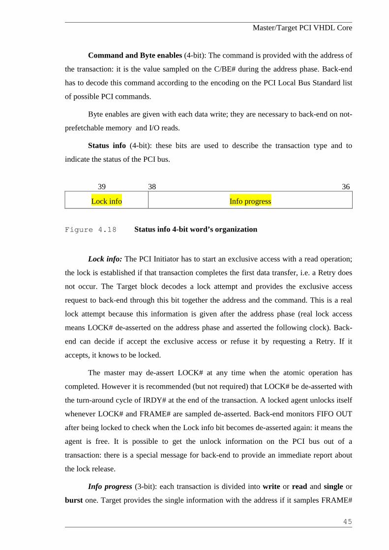
Status info (4-bit): these bits are used to describe the transaction type and to
indicate the status of the PCI bus.
39 38 36
Lock info Info progress
Figure 4.18 Status info 4-bit word’s organization
Lock info: The PCI Initiator has to start an exclusive access with a read operation;
the lock is established if that transaction completes the first data transfer, i.e. a Retry does
not occur. The Target block decodes a lock attempt and provides the exclusive access
request to back-end through this bit together the address and the command. This is a real
lock attempt because this information is given after the address phase (real lock access
means LOCK# de-asserted on the address phase and asserted the following clock). Back-
end can decide if accept the exclusive access or refuse it by requesting a Retry. If it
accepts, it knows to be locked.
The master may de-assert LOCK# at any time when the atomic operation has
completed. However it is recommended (but not required) that LOCK# be de-asserted with
the turn-around cycle of IRDY# at the end of the transaction. A locked agent unlocks itself
whenever LOCK# and FRAME# are sampled de-asserted. Back-end monitors FIFO OUT
after being locked to check when the Lock info bit becomes de-asserted again: it means the
agent is free. It is possible to get the unlock information on the PCI bus out of a
transaction: there is a special message for back-end to provide an immediate report about
the lock release.
Info progress (3-bit): each transaction is divided into write or read and single or
burst one. Target provides the single information with the address if it samples FRAME#

Master/Target PCI VHDL Core
46
de-asserted the following clock the address phase. This means that if single info is given
to the back-end application, this can be sure this is a single cycle. In case of burst
sometimes a master can delay the assertion of IRDY# for the first data transfer; FRAME#
has to remain asserted the clock following the address phase even if it is a single
transaction. This is not a problem because Target provides the last data or stop message in
any case.
When the 32-bit Address and data write are carrying write data or 4-bit Command
and Byte enables the BEs of not-prefetchable read, this is indicated by a Data Valid info;
the final data is marked as Last Data.
Target has to stop a prefetchable read, by writing into FIFO OUT a Stop_message.
It is possible getting the unlock protocol on the PCI bus at any time; back-end is
informed about the end of an exclusive operation as soon as the Target decodes it on the
bus. When this occurs out of a transaction there is a special message about Lock_release.
Table 4.5 shows the encoding of these three bits:
Bit[38] Bit[37] Bit[36] Description
0 0 0 Single write
0 0 1 Burst write
0 1 0 Single read
0 1 1 Burst read
1 0 0 Lock release
1 0 1 Data valid
1 1 0 Last data
1 1 1 Stop info
Table 4.5 Status info encoding

Master/Target PCI VHDL Core
47
4.4 EXTERNAL SIGNALS
Three signals are used out of FIFOs to carry some information, which need to be
provided to/from back-end application real-time without the timing separation of the fifo
buffer memories.
• Halt (PCI Core-Target Block => Back-end user)
• Shutdown (PCI Core-Target Block => Back-end user)
A Special Cycle command is like any other bus command where there is an address
and a data phase. The uniqueness of this command compared to the others is that no agent
responds with the assertion of DEVSEL# and the transaction concludes with a Master
Abort termination, which is a normal one. The broadcast message is valid on the first clock
IRDY# is asserted: there are two possible messages according to the Standard definition,
Halt and Shutdown. They are decoded by the Target block, which reports the message to
back-end as soon as it has been decoded.
• Posting_en (Back-end user => PCI Core- Master Block)
The Posting of Memory Write transactions is a way to improve the performance
optimization of the PCI system. Posting means the transaction is captured by an
intermediate buffer: the transaction completes at the source before it actually completes at
the intended destination. This allows the source to proceed with the next operation while
the transaction is still making its way through the system to its ultimate destination.
While posting improves system performance, it complicates event ordering. A
device can never make the acceptance (posting) of memory write transaction as a target
contingent on the prior completion of a non-posted transaction as a Master. Otherwise a
deadlock may occur. To be compliant with this specification, because the PCI Core is a
Master and Target Bus Interface, the master side of the local user can unable posting by
de-asserting the Posting_en signal.

Master/Target PCI VHDL Core
48
5. FUNCTIONAL BLOCKS
The PCI Core is an interface, which is used to connect an agent, that is both master
and target, to the PCI Local Bus. Because of this double capability the PCI Core is divided
into a Master Block, a Target Block and a Configuration Block.
There is a clear division between the master and the target part, not only from the
functional, but also from the architectural point of view. These two parts have its own state
machine that can operate independently from other in order to avoid possible deadlocks.
Although it should be possible to build the other functions into single blocks with
master/slave capability, a separation between the two parts was chosen.
Except from the Configuration block, the others are divided into four functional
parts: the relevant description was provided in the Chapter 2, Bus Sequencer Architecture.
In this section each unit will be describe with more details about its architecture and its
functional behavior. 5.1 MASTER FUNCTIONAL DESCRIPTION
The Master block consists of five different blocks as shown in Fig. 5.1.
Figure 5.1 Master Block of the PCI Core
MASTER STATE
MACHINE
FIFO OUT BLOCK
MASTER
FIFO IN BLOCK
MASTER
PARITY&ERROR MASTER
AD/CBE BUFFERS

Master/Target PCI VHDL Core
49
5.1.1 Master State Machine
This block manages the right PCI protocol for all supported commands, driving the
interface control signal of the PCI bus.
FRAME# is driven active during the transaction and it is de-asserted for the last
data phase or because of Master Abort, Target Abort, or Retry. There is another end-
condition, which is called time-out: the GNT# line is de-asserted and the Latency Timer
has expired. A special condition is the timer expiration during a Memory Write &
Invalidate command: the master has to complete the transfer of the entire current
cacheline; this feature is achieved thanks to a cacheline counter, which is implemented into
the Master State Machine.
IRDY# is driven according to an internal ready signal, which depends on the FIFO
full condition and the back-end ability to provide or accept data. As soon as a Master or
Target Abort, a Retry or a time-out condition are detected, IRDY# is asserted
independently of the ready signal to permit an immediate stop of the transaction. A similar
immediate stop occurs when the 8-clock rule about the Master Data Latency requirement is
not complied.
LOCK# is asserted to keep its ownership even if the Master is not working on the
bus; it is de-asserted as soon as an Abort termination is detected or when the first read
exclusive attempt finishes because of a Retry.
REQ# is used to request the ownership of the bus to the central arbiter when there is
a pending request from the back-end application. After a Target STOP# termination the
state machine goes to the Stop Turn Around state and REQ# is de-asserted at least for two
PCI clocks.
The Master State Machine has a simple Lock State Machine for handling the
exclusive access and a synchronous Main State Machine for the general control. The last
one consists of six states (Fig. 5.2):
• Idle is the state where the Master waits for a request from FIFO IN block.
• Addr is an one clock state; it is used to implement the address phase driving the
address and the command. This state is reached after a request from back-end when the
PCI Bus is not busy and the Master has got the grant from the arbiter.

Master/Target PCI VHDL Core
50
• M_Data is where data is transferred; there is a path to Addr because the Master PCI
Core supports the Fast back-to-back transaction.
• Turn_Ar is the state for de-asserting signals in preparation for tri-stating them. It is
required on all signals that may be driven by more than one agent to prevent
contention.
• Stop_Turn_Ar has the same function as the previous state but it is reached after a
Target Initiated Termination in order to de-assert the REQ# signal.
• Bus_Park occurs when GNT# has been asserted and the Master has not pending
requests from back-end user. The Master has to drive PCI signals as the Bus Parking
protocol requires.
Figure 5.2 State diagram of the Main State Machine
Idle
Addr
Bus_Park
M_Data
Turn_Ar
Stop Turn_Ar

Master/Target PCI VHDL Core
51
The Lock State Machine consists of two states as shown in Fig. 5.3:
• Free is the state which indicates that the Master has the current ownership of the
LOCK# or it is not driven by any agent.
• Busy means that another master is keeping the ownership of the LCOK# signal.
Figure 5.3 State diagram of the Lock State Machine
A part of the Master State Machine is dedicated to the generation of the read-
request signal to FIFO IN. This signal is asserted when the Master itself changes the value
of the AD lines (at the beginning and the end of the address phase and after each data
transfer, when both TRDY# and IRDY# are asserted).
This block samples write data coming from FIFO IN (Ad-int => Ad_Master_int,
Fig. 5.4) and data from the PCI AD lines during reads (AD_In => Data_Read_int, Fig.5.5)
Figure 5.4 Internal data path for address and data write
Free
Busy
Ad_int Ad_Master_int

Master/Target PCI VHDL Core
52
Figure 5.5 Internal data path for data read
Fig. 5.6 shows the path for the byte enables and the commands: they are provided
by the FIFO IN block. During a prefetchable read Cbe_Master_int takes the default value
0000. When the Memory Write & Invalidate enable bit of the Command Register has a
value of 0, the Master drives the encoding of the Memory Write into the Cbe_Master_int.
Figure 5.6 Internal path for command and byte enables
This block implements the general functions of the Master Block and provides
internal control signals to support the other blocks; this avoids the propagation of the PCI
control signals to the back-end side.
Cbe_int Cbe_Master_int
AD_In Data_Read_int

Master/Target PCI VHDL Core
5.1.2 Master AD/CBE Buffers
This block connects the 32-bit bi-directional and multiplexed PCI AD bus to the
two 32-bit unidirectional buses. AD_In are provided to the Master State Machine for
sampling data during read operations; Address/Write data and Command/Byte enables
come from internal data path and are put out to the bus lines through tri-state ports
controlled by the Master State Machine with output enable signals.
Fig. 5.7 shows the data path for the AD port, which is bi-directional for the Master
Block; Fig.5.8 indicates the tri-state buffer for the CBE port, output for the Master Block.
Figure 5.7 Master internal d
Figure 5.8 Output tri-state b
AD 32
CBE
4
OE_AD
ata path
uf
Ad_Master_int
AD_In
OE_CBE53
fer of the Master CBE lines
Cbe_Master_int

Master/Target PCI VHDL Core
5.1.3 FIFO IN Block Master
This block decodes the information coming from back-end application through
FIFO IN and drives the requests to the Master State Machine with the right timing. Fig.5.9
shows the path of the 40-bit input bus, which represents the value of the last word read
from FIFO IN. Address / data write are provided to the Master State Machine by
Ad_int_first and command / byte enables by Cbe_int_first.
Figure 5.9 Internal path of the 40-bit input
Fig: 5.10 indicates a list of internal request signals decoded by the combinatory
logic DECOD_A, DECOD_B and DECOD_C. Ignored_int becomes asserted when back-
end application has requested a not-supported command.
Figure 5.
Req_int_0
Req_int_1 Req_int_2
Req_int_3
DECOD_A
DECOD_B
DECOD_C
40
Data in
4
32
4
Ad_int
Cbe_int
Req_int_1
Req_int_0
Req_int_2
Req_int_3
Req_int_1Req_int_0
Cbe int
10 Combinatory logic for decoding b
Request_int Pref_int Ready_int
Stop_int Lock_req_int FtSA_int
Sp_Cycle_int R_W_int MWI_int Ignored_int
54
ack-end’s requests

Master/Target PCI VHDL Core
55
The output request signals are provided to the Master State Machine by a Type
Request Logic, which is a combinatory block under the control of an internal state machine
(Fig:5.11).
Figure 5.11 Generation of the request signals
The FIFO IN Block state machine consists of four different states, as shown in
Fig:5.12:
Figure 5.12 State diagram of the FIFO IN Block state machine
COMB. LOGIC
DECODER
TYPE
REQUEST LOGIC
STATE MACHINE
No_Req
PartialFlush
Data
Pending
40
4
32
4

Master/Target PCI VHDL Core
56
• No_Req is the state where the machine waits for a new request from back-end
application. FIFO IN is empty.
• Pending is reached as soon as the address is read from FIFO IN, request signals are
asserted and the machine waits for the beginning of the transaction on the PCI side
(FRAME# asserted).
• Data reflects the data phase on the PCI bus. It is present a path to Pending in order to
allow fast back-to-back transactions.
• P_Flush is used to read data from FIFO IN till the last data of operations with
abnormal termination or not-supported (ignored) commands from back-end user.
This block generates a signal, which drives, together (logic OR) with the one
coming from the Master State Machine, the read request for reading from FIFO IN. The
address is read by this block when the state machine is in the Idle state; if Master State
Machine wanted read a new data but FIFO is empty, it is FIFO IN Block’s responsibility
read this data as soon as a new word is pushed into FIFO. Read signal is asserted when the
state machine is making the partial flush or after a prefetchable request, when the master is
waiting for the Stop message.
The read signal coming from the Master State Machine and the one coming from
this block work as asynchronous request: data is provided after the rising edge of this read
request signal.
5.1.4 FIFO OUT Block Master
This block provides the information to back-end application by writing 40-bit
words into FIFO OUT.
A final info about the result of the transaction is written at the end of a write PCI
operation with the right timing: it is necessary waiting for the error result of the last data
transfer. Each read data is reported to back-end with other info (parity error is detected by
an internal parity checking and not by sampling PERR# line as in a write: this information
occurs one clock before respect to the write case).

Master/Target PCI VHDL Core
Read data come from the Master State Machine through Read_Data_int bus, which
is the one clock delayed copy of PCI AD lines during read data transfers. There is another
sampling block on this path in order to get read data with a two PCI clock delay, i.e.
synchronous with the parity error response (Fig. 5.13).
Figure 5.13 One clock delay path for read data
The other 8 bits of the 40-bit output word written into FIFO have a particular path, as
shown in Fig. 5.14, for handling full conditions, i.e. when FIFO OUT becomes full. If
Master is reading at full speed there will be three extra read (one not written word before
the assertion of the full signal , two extra not written read after full).
Figure 5.14 Interna
Read_Data_int_int
Read_Data_int
2 clk delay
4
Ownlock
First data
1 clk delay
r
Type end
Info latch1
4Data bit
Parity erro
57
l path of end type and status info 8 bits
8
Info latch2

Master/Target PCI VHDL Core
58
A parallel three-level latch system is necessary to store 40-bit word in the worst
case (FIFO OUT full when Master is reading at full speed). The path indicated in Fig: 5.15
completes this latch system (Data_out_aux, Info_latch1 and Info_latch2).
Write signal requests a writing operation, which will occur the next rising edge of
PCI clock.
Figure 5.15 Data out path of the FIFO OUT Block Master
5.1.5 Master Parity & Error Block
The Parity & Error block generates the parity and checks possible parity errors for
the Master side of the PCI Core.
The agent that is driving the PCI AD bus has to calculate and manage the parity line
of the bus, which is called PAR. Master drives PAR during the address phase of each
transaction it is implementing and the data phase of write operations. The number of “1”s
on AD, CBE# and PAR equals an even number. The timing requirements of PAR signal
are supported thanks to the control of the Master State Machine, which enables the output
buffer of PAR.
Fig. 5.16 illustrates the generation of PAR through two different XOR-trees. The
output value is delayed by one PCI clock to achieve timing requirements on this signal.
Data_out_int Data_out_aux
Data_out

Master/Target PCI VHDL Core
Fig. 5.17 shows the XOR-tree to calculate the PAR_CBE internal signal; the same
structure is used to get PAR_AD from the AD_Master_int 32-bit line.
Figure 5.16 Internal path for the calculation of parity
Figure 5.17 XOR tree for the generation of PAR_CBE signal
This block also manages the checking of possible parity errors and d
signal during read data phase; it works during writes as well to report error i
FIFO OUT block. The general structure of the parity error checker is shown i
Figure 5.18 Parity checker overview
XOR
XORAD_Master_int
PAR_AD
XOR
XOR
XORt
E
PAR_In
Data_Read_int
XOR TREE
XOR
CBE_Master_int PAR_CBE
PAR_Out
CBE Master in
riv
nfo
n F
XO
PAR CBE
es PERR#
rmation to
ig. 5.18.
R
PAR CB
PERR_Out
Parity Error
59

Master/Target PCI VHDL Core
60
5.2 TARGET FUNCTIONAL DESCRIPTION
Figure 5.19 shows the organization of the Target Block, which consists of four
different blocks.
Figure 5.19 Target Block of the PCI Core
5.2.1 Target State Machine
This block implements the main functions of the Target Block of the PCI Core; it
drives the interface control signals of the PCI bus, handling the bus handshake with the
master of the PCI transaction.
DEVSEL#, TRDY# and STOP# are sustained tri-state signals and are driven by tri-
state output buffers enabled with internal signals.
DEVSEL# is asserted to claim the transaction, two clocks after the PCI address
phase when this slave is targeted by the master for the current operation. This means that
TARGET STATE
MACHINE
FIFO BLOCK TARGET
PARITY&ERROR TARGET
AD/CBE BUFFERS

Master/Target PCI VHDL Core
61
the PCI Core, as Target, implements the medium decode. DEVSEL# is de-asserted at the
end of the transaction or when a Target Abort occurs.
TRDY# is active when the back-end application is ready for data transfer: it is de-
asserted after a data transfer during a not-prefetchable read or an I/O access to get time for
sampling byte enables and providing them to back-end. When it becomes ready it is
asserted again and a new data transfer occurs. The other operations can complete with
zero-wait cycles.
STOP# is driven active when the target is going to implement a Target Termination.
All kind of termination are supported: Retry, Disconnect with or without data and Target
Abort.
Target handles exclusive access; a partial lock of a BAR is supported instead of a
complete resource locking. When the Target is locked, an attempt by another master to the
locked BAR is stopped by a Retry. Fig. 5.20 shows the state diagram of the Lock State
Machine, which consists of two state.
Figure 5.20 State diagram of the Target Lock Machine
Free: the target becomes free, i.e. not locked after a lock access, when it samples
FRAME# and LOCK# de-asserted.
Locked: the machine goes to this state when a memory access occurs and LOCK#
is de-asserted during the PCI address phase and active the following rising clock edge.
This means that target will become locked only because of a real lock attempt. In fact
LOCK# is de-asserted during the address phase even if the current access is not a lock one.
This block has also a Main State Machine that implements the main functions and
decodes the different possible situations of the PCI bus. It consists of six states, as shown
in Fig. 5.21.
Free
Locked

Master/Target PCI VHDL Core
62
Figure 5.21 State diagram of the Main State Machine
Idle: it indicates that an idle state is on the PCI bus; no master is implementing any
PCI transaction. As soon as FRAME# is sample asserted, i.e. there is an address phase, the
State Machine goes to Addr.
Addr: the address has been decoded by the Address decoder in the Configuration
Block and Target can check the Hit lines to understand if it is the actual slave of the current
transaction. The address decoder compares the PCI address with the BAR value; the Target
State Machine decodes the command and enables the I/O, Configuration or Memory hit
signals. A memory access to a locked BAR is terminated with an automatic Retry (path to
Targ_Term). When Target is not involved in the current transaction (hit signals de-
asserted) the machine goes to Not_Inv or Idle (if FRAME# has just been de-asserted).
T_Data: this state implements the PCI data phase where data transfers occur. At
any time the transaction can be stopped (path to Targ_Term) because of Abort or Stop
Idle
Addr
Not Inv
Turn Ar
Target Termin
T_Data

Master/Target PCI VHDL Core
63
request from back-end application. A Disconnect occurs after the expiration of the timer
for the Data Latency rules (16-clock for the first data and 8-clock for the subsequent one).
A combinatory block called Addr_Checker checks the correct value of the two bits
AD[1..0]: linear incrementing mode is supported and the Wrap mode when wrap enable
from the Configuration region has value of ‘1’. If an error is detected a Disconnect after
the first data transfer occurs.
Not_Inv: it means not involved, i.e. the target is not the actual slave of the current
PCI transaction.
Turn_Ar: this state implements the turn around cycle. The path to Addr is for
decoding Fast back-to-back protocols.
Targ_Term: in this state STOP# is asserted to implement a target termination.
When FRAME# is ‘1’ and IRDY# is ‘0’ the turn around cycle can occur.
This block samples address / write data and command / byte enables from the AD
and CBE# PCI lines. Fig. 5.22 illustrates the internal unidirectional multiplexed address /
data path and describes the path for command and byte enables; it is also indicated the
combinatory logic for the command decoding.
Figure 5.22 Internal ad and cbe buses
The Target State Machine block manages the Special Cycle command without
affecting any other target block. The message is decoded and the result is provided directly
to back-end application by two external signals called HALT and SHUTDOWN.
Ad_Target_int AD_In
Cbe_Target_int
CBE_In Comm decoder

Master/Target PCI VHDL Core
During a PCI Configuration access burst read and write data transfers are supported
with zero-wait states thanks to an internal adder which increments the address for
providing it to the Configuration Block.
5.2.2 Target AD/CBE Buffers
This block connects the 32-bit bi-directional and multiplexed PCI AD bus to the
two 32-bit unidirectional buses. AD_In are provided to the Target State Machine for
sampling data during write operations. Command/Byte enables are only input for the
Target Block: CBE_In are provided to the Target State Machine as AD_In.
Read data come from back-end application through FIFO IN (Data_Read_int) or
from the Configuration Space (Data_Read_CONF). A multiplexer controlled by the Target
State Machine selects the right path, which is put out to the bus lines through tri-state ports
controlled by the Target State Machine with output enable signals (Fig.5.23).
Figure 5.23 Internal Data path of t
AD
OE_AD
he Target Block
D
Data_Read_int
64
ata_Read_CONF

Master/Target PCI VHDL Core
65
5.2.3 FIFO Block Target
This block manages the handshake with back-end application through FIFO IN and
FIFO OUT. There is a State Machine, which has four valid states and all possible
transactions are divided into Memory Write, Memory Read (prefetchable and not-
prefetchable), I/O read / write and Configuration read / write (Fig.5.24).
Figure 5.24 State diagram of the State Machine in the FIFO Block Target
Idle: The machine is in the Idle state when the Target Block is not involved in any
PCI transaction.
Mem_W: The Target block is implementing a memory Write; it supports Posting
Data. When the Machine goes to Mem_W the FIFO block writes the address and the
command into FIFO OUT. If this FIFO is full or Posting enable is not active this block
requests a stop, i.e. the target Block will issue a Retry. At any time back-end can disable
posting data in order to avoid deadlock situations: a Disconnect will occur. There is a
particular data path to support a possible full condition of FIFO OUT (Fig.5.25).
Mem_R: The Target State Machine has requested a Memory Read access. They are
possible if there are not posted data into FIFO OUT; otherwise the FIFO block requests a
Retry termination.
Idle
Not Mem
Mem_R
Mem_W

Master/Target PCI VHDL Core
Figure 5.25 Data path for writing 40-bit word into FIFO OU
Byte enables are written into FIFO OUT for not-prefetchable ope
end has to provide the next data. It is not necessary writing BEs during
At the end of the transaction a stop message is given to back-end and FIF
Not_Mem: This state is used to implement I/O and Config
operations. When FIFO OUT is not empty, these accesses cannot occur:
the expiration of a retry-counter. After that FIFO will be flushed. PCI Co
are reported to back-end through FIFO OUT without any interactio
application.
5.2.3 Target Parity & Error Block
This block has the responsibility to drive the PAR, PERR# and SE
Target provides the parity on the PAR line during the data phase of read
5.26 shows the architecture of the parity generator, which consists of t
the PCI CBE# lines are sampled for reducing the input delay on this PCI
40
Data_out to FIFO OUT
66
T
rations; then back-
prefetchable read.
O IN is flushed.
uration read/write
there is a Retry till
nfiguration cycles
n with back-end
RR# PCI signals.
transactions. Fig.
wo trees of XOR;
input path.

Master/Target PCI VHDL Core
67
Figure 5.26 Structure of the parity generator
The checker is a parity checker and drive PERR# signal during write data phases.
SERR# is used only to report parity errors during address phases and Special Cycles. The
functional and structural organization of the parity checker is shown in Fig. 5.27.
Figure 5.27 Parity checker of the target block
Fig. 5.28 shows the PAR port which is an input-output one; the output is driven, as
for PERR# and SERR#, with tri-state buffers which are controlled by the enable signals
generated by the Target State Machine.
Figure 5.28 PAR input – output port
CBE
Data_Read_bus
XOR TREE
XOR TREE
PAR_Out
AD_Target_int
XOR TREE
CBE
XOR TREE
PAR_In
Parity error
OE_PAR
PAR_Out
PAR_In PAR

Master/Target PCI VHDL Core
68
5.3 CONFIGURATION BLOCK
The Configuration Block consists of the Configuration Space, the support for
handling PCI Configuration cycles and back-end direct accesses and the logic block for the
address decoding.
The PCI Core supports a predefined header region type 00h and table 5.1 indicates
which registers are read & write (shaded regions).
Address Byte 3 Byte 2 Byte 1 Byte 0
00h DEVICE ID VENDOR ID
04h STATUS REGISTER COMMAND REGISTER
08h CLASS CODE REVISION ID
0Ch BIST HEADER TYPE LATENCY TIMER CACHELINE SIZE
10h BASE ADDRESS REGISTER 0
14h BASE ADDRESS REGISTER 1
18h BASE ADDRESS REGISTER 2
1Ch BASE ADDRESS REGISTER 3
20h BASE ADDRESS REGISTER 4
24h BASE ADDRESS REGISTER 5
28h CARDBUS CIS POINTER
2Ch SUBSYSTEM ID SUBSYSTEM VENDOR ID
30h EXPANSION ROM BASE ADDRESS REGISTER
34h RESERVED
38h RESERVED
3Ch MAX _LAT MIN_GNT INTERRUPT PIN INTERRUPT LINE
Table 5.1 Type 00h Configuration Space Header

Master/Target PCI VHDL Core
69
Reserved 9 8 7 6 5 4 3 2 1 0
Table 5.2 Layout of the Command Register
15 14 13 12 11 10 9 8 7 6 5 Reserved
Table 5.3 Layout of the Status Register
Table 5.2 and table 5.3 indicate the layout of the Command and Status registers:
shaded regions shows read & write bit-register.
The support for handling read and write accesses to the Configuration Space has a
State Machine, which makes the control and the data handshake. An access to the
Configuration registers is possible from the PCI and the local user side; it is necessary an
arbitration between these two possible masters, the PCI one and the back-end application.
The State Machine deals with these problems and consists of three states, as shown in Fig.
5.29.
Figure 5.29 State diagram of the Configuration Block
Idle: there are not accesses to the Configuration Space neither from the PCI side
nor from back-end local interface. When a PCI request occurs at the same time of a back-
Idle
Busy BACK
Busy PCI

Master/Target PCI VHDL Core
end one, the machine goes to the Busy PCI, giving the priority to the PCI Master, which is
implementing the Configuration cycle.
Busy_PCI: in this state a Configuration Read or Write is occurring. Any back-end
attempt is not accepted (Ack_BACK is kept de-asserted) and data on the output bus are
indicated not-valid.
Busy_BACK: back-end is writing a 32-bit word into the Configuration Space. A
PCI request is stopped with a Retry command to the Target State Machine.
The Configuration Space is divided into 32-bit lines and each line into four bytes:
the write operation from the PCI bus is controlled by the Byte enables. The granularity of
the access from back-end side is not byte: local user is allowed to write only with single
32-bit cycles.
Figure
...
Data_in_back
Write_back Write_PCI
O
70
5.30 Write support of the Configuration Block
...
CBE Ad_Target_int

Master/Target PCI VHDL Core
71
Fig. 5.30 shows the structure of the support for writing into the Configuration
Space: there are two separate input data paths with different de-multiplexer blocks. The 32-
bit line is selected with the write signal: for PCI Configuration Write accesses, byte
enables are used to indicate the byte selected inside the line.
There are two multiplexer blocks for providing read data, as shown in Fig. 5.31.
Figure 5.31 Support for reading from Configuration Space
The Address Decoder is a simple comparator: when the value of the AD_Target_int
bus is equal to the one written in the Base Address Register an Hit signal is asserted. It is
possible indicate if the BAR selected refers to the Memory or I / O space. This block drives
also the prefetchable signal, which reports the value of the bit 3 of memory BARs.
...
...
Data_Read_CONF
Data_out_back

Master/Target PCI VHDL Core
72
6. VHDL CODE OVERVIEW
This section wants to provide a guide for reading and checking the VHDL code
attached in the APPENDIX A. The design was carried out in a hierarchical and modular
way; the functional organization of the PCI Core was kept during the writing of the VHDL
code.
6.1 VHDL FILE NAMES
Figure 6.1 shows the VHDL organization of the PCI Core.
Figure 6.1 VHDL file names and organization
PCI CORE Block
Master_Block Configuration Block Target Block
MSM
FIFO IN Mblock
FIFO OUT Mblock
Parity & Error M
AD CBE Mbuffer
TSM
FIFO Tblock
Parity & Error T
AD CBE Tbuffer

Master/Target PCI VHDL Core
73
REFERENCES • PCI Local Bus Standard, Revision 2.1 – June 1995, PCI Special Interested Group
* PCI Hardware and Software architecture & design – March 1995, E.Solari &
G.Willse

Master/Target PCI VHDL Core
74
APPENDIX A: VHDL CODE