Embed Size (px)
Citation preview
LTC6091
16091fa
For more information www.linear.com/LTC6091
TYPICAL APPLICATION
FEATURES DESCRIPTION
Dual 140V, Rail-to-Rail Output, Picoamp
Input Current Op Amp
The LTC®6091 is a dual, high voltage precision operational amplifier. The low noise, low bias current input stage is ideal for high gain configurations. The LTC6091 has low input offset voltage, a rail-to-rail output stage, and can be run from a single 140V or split ±70V supplies.
The LTC6091 is internally protected against overtemper-ture conditions. A thermal warning output, TFLAG, goes active when the die temperature approaches 150°C. The output stage can be turned off with the output disable pin OD. By tying the OD pin to the thermal warning output, the part will disable the output stage when it is out of the safe operating area. These pins easily interface to any logic family.
The LTC6091 is unity-gain stable with up to a 200pF output capacitor. A wide input and output common mode range along with many features makes the LTC6091 useful for many high voltage applications.
High Voltage Analog MUX VOUT vs Time
APPLICATIONS
n Supply Range: ±4.75V to ±70V (140V)n 0.1Hz to 10Hz Noise: 3.5μVP-Pn Input Bias Current: 50pA Maximumn Low Offset Voltage: 1.25mV Maximumn Low Offset Drift: ±5μV/°C Maximumn CMRR: 130dB Minimumn Rail-to-Rail Output Stagen Output Sink and Source: 50mAn 12MHz Gain-Bandwidth Productn 21V/μs Slew Raten 11nV/√Hz Noise Densityn Thermal Shutdownn 4mm × 6mm 16-Lead QFN Package
n ATEn Piezo Driversn Photodiode Amplifiern High Voltage Regulatorsn Optical Networking
L, LT, LTC, LTM, Linear Technology, the Linear logo and Over-The-Top are registered trademarks of Linear Technology Corporation. All other trademarks are the property of their respective owners.
–
+1/2 LTC6091
10k
10k
CHAIN
100k
COMA
SELECTCHA/CHB
ODA
–
+1/2 LTC6091
10k
10k
CHBIN
100k
COMB
MUX OUT
CHAIN = 10VP-P, 20kHz SINECHBIN = 5VP-P, 20kHz TRIANGLE
6091 TA01a
ODB
TIME (200µs/DIV) 6091 TA01b
CHB CHBCHA
10SELECT
CHA/CHB10V/DIV
MUX OUT20V/DIV
0

LTC6091
26091fa
For more information www.linear.com/LTC6091
PIN CONFIGURATIONABSOLUTE MAXIMUM RATINGS
Total Supply Voltage (V+A to V–, or V+B to V–) .......150VCOMA .............................................................. V– to V+ACOMB ............................................................... V– to V+BInput Voltage ODA ..................................................V– to V+A + 0.3V ODB ..................................................V– to V+B + 0.3V +INA, –INA .............................V– – 0.3V to V+A + 0.3V +INB, –INB .............................V– – 0.3V to V+B + 0.3V ODA to COMA, ODB to COMB ..................... –3V to 7VInput Current +INA, –INA, +INB, -INB .................................... ±10mATFLAGA, TFLAGB Output TFLAGA ..................................V– – 0.3V to V+A + 0.3V TFLAGB ..................................V– – 0.3V to V+B + 0.3V TFLAGA to COMA ........................................ –3V to 7V TFLAGB to COMB ........................................ –3V to 7VContinuous Output Current OUTA , OUTB (Note 2) ................................ 50mARMSOperating Junction Temperature Range (Note 3) ............................................. –40°C to 125°CSpecified Junction Temperature Range (Note 4) LTC6091I .............................................–40°C to 85°C LTC6091H .......................................... –40°C to 125°CJunction Temperature (Note 5) ............................. 150°CStorage Temperature Range .................. –65°C to 150°CLead Temperature (Soldering 10sec)..................... 300°C
(Note 1)
7
TOP VIEW
17V–
UFE PACKAGE32(16)-LEAD (4mm × 6mm) PLASTIC QFN
8
16 15
11
12
13
5
4
3
2
–INA
+INA
V–
COMB
V+A
V+B
OUTB
OUTA
TFLAGA
ODB
–INB
+INB
V–
TFLA
GB
COM
A
ODA
9
10
14
6
1
θJC = 15°C/W
EXPOSED PAD (PIN 17) IS V–, MUST BE SOLDERED TO PCB
ORDER INFORMATIONLEAD FREE FINISH TAPE AND REEL PART MARKING* PACKAGE DESCRIPTION TEMPERATURE RANGE
LTC6091IUFE#PBF LTC6091IUFE#TRPBF 6091 16-Lead Plastic QFN –40°C to 85°C
LTC6091HUFE#PBF LTC6091HUFE#TRPBF 6091 16-Lead Plastic QFN –40°C to 125°C
Consult LTC Marketing for parts specified with wider operating temperature ranges. *The temperature grade is identified by a label on the shipping container.Consult LTC Marketing for information on nonstandard lead based finish parts.For more information on lead free part marking, go to: http://www.linear.com/leadfree/ For more information on tape and reel specifications, go to: http://www.linear.com/tapeandreel/
LTC6091
36091fa
For more information www.linear.com/LTC6091
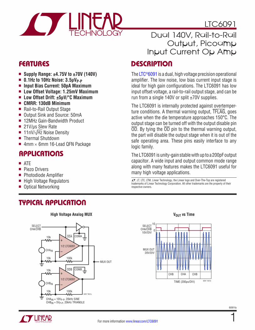
ELECTRICAL CHARACTERISTICS The l denotes the specifications which apply over the full operating temperature range, otherwise specifications are at TA = 25°C. Test conditions are V+ = 70V, V– = –70V, VCM = VOUT = 0V, VOD = open unless otherwise noted.
SYMBOL PARAMETER CONDITIONS I-SUFFIX H-SUFFIX
UNITSMIN TYP MAX MIN TYP MAX
VOS Input Offset Voltage
l
±330 ±330
±1000 ±1250
±330 ±330
±1000 ±1250
μV µV
∆VOS/∆T Input Offset Voltage Drift TA = 25°C, ∆TJ = 70°C –5 ±3 5 –5 ±3 5 µV/°C
IB Input Bias Current (Note 6) Supply Voltage = ±70V Supply Voltage = ±15V Supply Voltage = ±15V
l
3 0.3
50
3 0.3
800
pA pA pA
IOS Input Offset Current (Note 6) Supply Voltage = ±15V
l
0.5 30
0.5 120
pA pA
en Input Noise Voltage Density f = 1kHz f = 10kHz
14 11
14 11
nV/√Hz nV/√Hz
Input Noise Voltage 0.1Hz to 10Hz 3.5 3.5 µVP-P
in Input Noise Current Density 1 1 fA/√Hz
VCM Input Common Mode Range Guaranteed by CMRR
l
V– + 3V
±68 V+ – 3V
V– + 3V
±68 V+ – 3V
V V
CIN Common Mode Input Capacitance
9 9 pF
CDIFF Differential Input Capacitance 5 5 pF
CMRR Common Mode Rejection Ratio
VCM = –67V to 67V
l
130 126
>140 130 126
>140 dB dB
PSRR Power Supply Rejection Ratio VS = ±4.75V to ±70V
l
112 106
>120 112 106
>120 dB dB
VOUT Output Voltage Swing High (Referred to V+) (VOH)
No Load ISOURCE = 1mA ISOURCE = 10mA
l
l
l
10 50
450
25 140
1000
10 50
450
25 140
1000
mV mV mV
Output Voltage Swing Low (Referred to V–) (VOL)
No Load ISINK = 1mA ISINK = 10mA
l
l
l
10 30
250
25 80
600
10 30
250
25 80
600
mV mV mV
AVOL Large-Signal Voltage Gain RL = 10k VOUT from –60V to 60V
l
1000 1000
>10000 1000 1000
>10000 V/mV V/mV
ISC Output Short-Circuit Current (Source and Sink)
Supply Voltage = ±70V Supply Voltage = ±15V
l
50
90 50
90 mA mA
SR Slew Rate AVCL = –4, RL = 10k
l
10
21 9
21 V/μs V/μs
GBW Gain-Bandwidth Product fTEST = 20kHz, RL = 10k
l
5.5
12 5
12 MHz MHz
φM Phase Margin RL = 10k, CL = 50pF 60 60 Deg
FPBW Full-Power Bandwidth VOUT = 125VP-P
l
20
40 18
40 kHz kHz
tS Settling Time 0.1% VSTEP = 1V, AV = 1, RL = 10k
2 2 µs
IS Supply Current (Per Amplifier) No Load
l
2.8 3.9 4.3
2.8 3.9 4.3
mA mA
VS Supply Voltage Range Guaranteed by the PSRR Test
l 9.5 140 9.5 140 V
LTC6091
46091fa
For more information www.linear.com/LTC6091
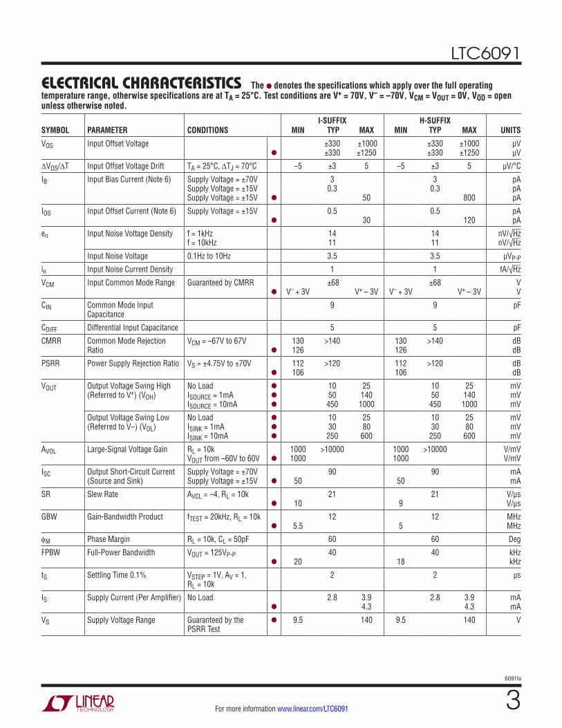
ELECTRICAL CHARACTERISTICS The l denotes the specifications which apply over the full operating temperature range, otherwise specifications are at TA = 25°C. Test conditions are V+ = 70V, V– = –70V, VCM = VOUT = 0V, VOD = open unless otherwise noted.
SYMBOL PARAMETER CONDITIONS I-SUFFIX H-SUFFIX
UNITSMIN TYP MAX MIN TYP MAX
ODH OD Pin Voltage, Referenced to COM Pin
VIH l COM + 1.8V
COM + 1.8V
V
ODL OD Pin Voltage, Referenced to COM Pin
VIL l COM + 0.65V
COM + 0.65V
V
Amplifier DC Output Impedance, Disabled
DC, OD = COM >10 >10 MΩ
COMCM COM Pin Voltage Range l V– V+ – 5 V– V+ – 5 V
COMV COM Pin Open-Circuit Voltage l 17 21 25 17 21 25 V
COMR COM Pin Resistance l 500 665 850 500 665 850 kΩ
TEMPF Die Temperature Where TFLAG Is Active
145 145 °C
TEMPHYS TFLAG Output Hysteresis 5 5 °C
ITFLAG TFLAG Pull-Down Current TFLAG Output Voltage = 0V
l 70 200 330 70 200 330 µA
Note 1: Stresses beyond those listed under Absolute Maximum Ratings may cause permanent damage to the device. Exposure to any Absolute Maximum Rating condition for extended periods may affect device reliability and lifetime.Note 2: Either output (OUTA or OUTB) of the LTC6091 is capable of producing peak output currents in excess of 50mA. Current density limitations within the IC require the continuous RMS current supplied by either output (sourcing or sinking) over the operating lifetime of the part to be limited to under 50mA (absolute maximum). Proper heat sinking may be required to keep the junction temperature below the absolute maximum rating. Refer to the Power Dissipation and Thermal Considerations section of the data sheet for more information.Note 3: The LTC6091I is guaranteed functional over the operating junction temperature range –40°C to 85°C. The LTC6091H is guaranteed functional over the operating junction temperature range –40°C to 125°C. Specifying the junction temperature range as an operating condition is applicable for devices with potentially significant quiescent power dissipation.
Note 4:The LTC6091I is guaranteed to meet specified performance from –40°C to 85°C. The LTC6091H is guaranteed to meet specified performance from –40°C to 125°C.Note 5: This device includes overtemperature protection that is intended to protect the device during momentary overload conditions. Operation above the specified maximum operating junction temperature is not recommended.Note 6: Input bias and offset current is production tested with ±15V supplies. See Typical Performance Characteristics curves of actual typical performance over full supply range.
LTC6091
56091fa
For more information www.linear.com/LTC6091
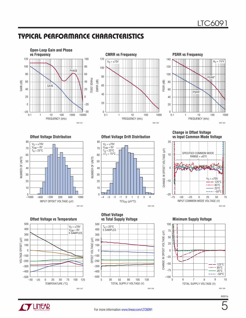
TYPICAL PERFORMANCE CHARACTERISTICS
Offset Voltage Distribution Offset Voltage Drift DistributionChange in Offset Voltage vs Input Common Mode Voltage
Offset Voltage vs TemperatureOffset Voltage vs Total Supply Voltage Minimum Supply Voltage
Open-Loop Gain and Phase vs Frequency CMRR vs Frequency PSRR vs Frequency
FREQUENCY (kHz)
40
20
GAIN
(dB)
PHASE (DEG)
80
120
0
60
100
0.1 10 100 1000 10000
6091 G01
–20
40
20
80
0
60
100
–20
–301
PHASE
GAIN
FREQUENCY (kHz)
40CM
RR (d
B)
80
120
20
60
100
0.1 10 100 1000
6091 G02
01
VS = ±70V
FREQUENCY (kHz)
40
PSSR
(dB) 80
120
140
0.1 10 100 1000
6091 G03
01
100
60
20
PSRR+
PSRR–
AV = 1V/V
INPUT OFFSET VOLTAGE (µV)–1000
NUM
BER
OF U
NITS
40
50
60
600
6091 G04
30
20
0–600 –200 200 1000
10
80VS = ±70VVCM = 0VTA = 25°C
70
TCVOS (µV/°C)–4
NUM
BER
OF U
NITS
40
50
60
3
6091 G05
30
20
0–3 –2 –1 0 1 2 4
10
80VS = ±70VVCM = 0VTA = 25°C∆TJ = 75°C
70
INPUT COMMON MODE VOLTAGE (V)–75
–20
CHAN
GE IN
OFF
SET
VOLT
AGE
(µV)
–10
0
10
20
–50 –25 0 25
6091 G06
50 75
VS = ±70V125°C85°C25°C–50°C
SPECIFIED COMMON MODE RANGE = ±67V
TEMPERATURE (°C)–50
–500
VOLT
AGE
OFFS
ET (µ
V)
–400
–200
–100
0
500
200
0 50 75 100
6091 G07
–300
300
400
100
–25 25 125
VS = ±70VVCM = 0V5 SAMPLES
TOTAL SUPPLY VOLTAGE (V)5
–500
OFFS
ET V
OLTA
GE (µ
V)
–300
–100
100
30 55 80 105
6091 G08
130
300
500
–400
–200
0
200
400TA = 25°C5 SAMPLES
TOTAL SUPPLY VOLTAGE (V)5
CHAN
GE IN
OFF
SET
VOLT
AGE
(µV)
–25
0
25
8 10
6091 G09
–50
–75
–1006 7 9
50
75
100
125°C85°C25°C–50°C
LTC6091
66091fa
For more information www.linear.com/LTC6091
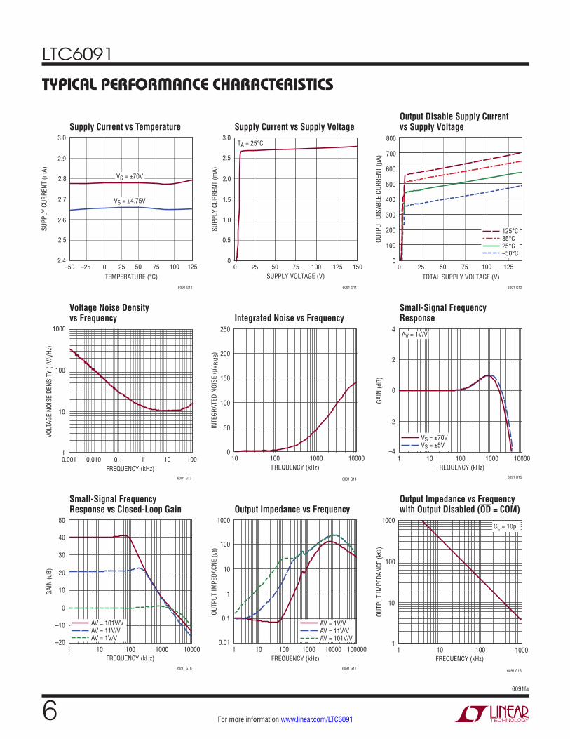
TYPICAL PERFORMANCE CHARACTERISTICS
Voltage Noise Density vs Frequency Integrated Noise vs Frequency
Small-Signal Frequency Response
Small-Signal Frequency Response vs Closed-Loop Gain Output Impedance vs Frequency
Output Impedance vs Frequency with Output Disabled (OD = COM)
Supply Current vs Temperature Supply Current vs Supply VoltageOutput Disable Supply Current vs Supply Voltage
TEMPERATURE (°C)–50
SUPP
LY C
URRE
NT (m
A)
2.8
2.9
3.0
25 75
6091 G10
2.7
2.6
–25 0 50 100 125
2.5
2.4
VS = ±70V
VS = ±4.75V
SUPPLY VOLTAGE (V)0
0
SUPP
LY C
URRE
NT (m
A)
0.5
1.0
1.5
2.0
3.0
25 50 75 100
6091 G11
125 150
2.5
TA = 25°C
TOTAL SUPPLY VOLTAGE (V)0
OUTP
UT D
ISAB
LE C
URRE
NT (µ
A)
400
6091 G12
200
050 10025 75 125
600
800
300
100
500
700
125°C85°C25°C–50°C
FREQUENCY (kHz)
10
VOLT
AGE
NOIS
E DE
NSIT
Y (n
V/√H
z)
100
0.001 0.1 1 10010
6091 G13
10.010
1000
FREQUENCY (kHz)10
0
INTE
GRAT
ED N
OISE
(µV R
MS)
150
200
250
100 1000 10000
6091 G14
100
50
FREQUENCY (kHz)
–2
GAIN
(dB)
0
2
4
1 100 1000 10000
6091 G15
–410
AV = 1V/V
VS = ±70VVS = ±5V
FREQUENCY (kHz)
0
GAIN
(dB) 20
40
50
1 100 1000 10000
6091 G16
–2010
30
10
–10 AV = 101V/VAV = 11V/VAV = 1V/V
FREQUENCY (kHz)
0.1
OUTP
UT IM
PEDA
CNE
(Ω)
1
10
100
1000
1 100 1000 100000
6091 G17
0.0110 10000
AV = 1V/VAV = 11V/VAV = 101V/V
FREQUENCY (kHz)1
1
OUTP
UT IM
PEDA
NCE
(kΩ
)
10
100
1000
10 100
6091 G18
1000
CL = 10pF
LTC6091
76091fa
For more information www.linear.com/LTC6091
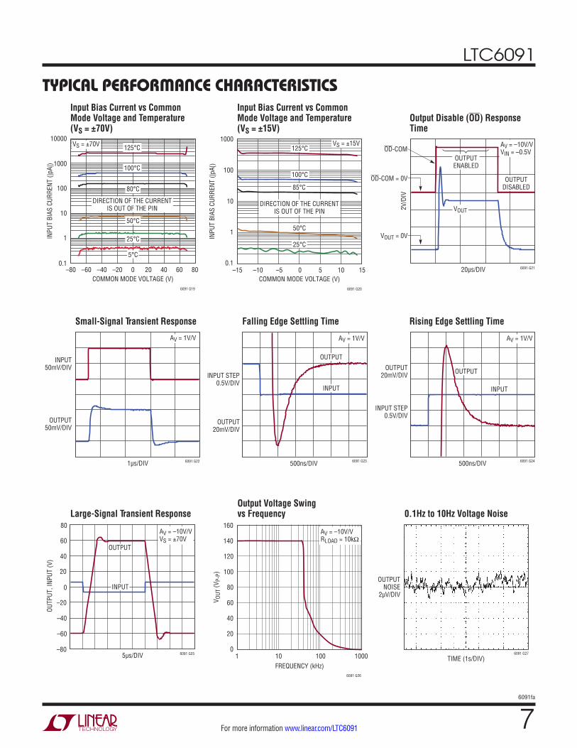
TYPICAL PERFORMANCE CHARACTERISTICS
Small-Signal Transient Response Falling Edge Settling Time Rising Edge Settling Time
Large-Signal Transient ResponseOutput Voltage Swing vs Frequency 0.1Hz to 10Hz Voltage Noise
Input Bias Current vs Common Mode Voltage and Temperature (VS = ±70V)
Input Bias Current vs Common Mode Voltage and Temperature (VS = ±15V)
Output Disable (OD) Response Time
COMMON MODE VOLTAGE (V)
10
INPU
T BI
AS C
URRE
NT (|
pA|)
100
–80 0 40
6091 G19
1
–40–60 20 60–20 80
125°CVS = ±70V
100°C
80°C
50°C
DIRECTION OF THE CURRENTIS OUT OF THE PIN
25°C
5°C0.1
1000
10000
COMMON MODE VOLTAGE (V)
1
INPU
T BI
AS C
URRE
NT (|
pA|)
100
1000
–15 5 15
6091 G20
0.1–5–10 100
10
125°C
100°C
VS = ±15V
50°C
25°C
85°C
DIRECTION OF THE CURRENTIS OUT OF THE PIN
INPUT50mV/DIV
OUTPUT50mV/DIV
6091 G221µs/DIV
AV = 1V/V
INPUT STEP0.5V/DIV
OUTPUT20mV/DIV
500ns/DIV 6091 G23
AV = 1V/V
INPUT
OUTPUT
INPUT STEP0.5V/DIV
OUTPUT20mV/DIV
500ns/DIV 6091 G24
AV = 1V/V
INPUT
OUTPUT
OUTP
UT, I
NPUT
(V)
0
20
40
6091 G25
–20
–40
–805µs/DIV
–60
80
60
INPUT
OUTPUT
AV = –10V/VVS = ±70V
FREQUENCY (kHz)1
80
V OUT
(VP-
P)
120
160
10 100 1000
6091 G26
40
60
100
140
20
0
AV = –10V/VRLOAD = 10kΩ
TIME (1s/DIV)
OUTPUTNOISE
2µV/DIV
6091 G27
6091 G2120µs/DIV
OD-COM
OD-COM = 0V
2V/D
IV
OUTPUTENABLED
OUTPUTDISABLED
VOUT = 0V
AV = –10V/VVIN = –0.5V
VOUT

LTC6091
86091fa
For more information www.linear.com/LTC6091
TYPICAL PERFORMANCE CHARACTERISTICS
Output Voltage Swing Low (VOL) vs Load Current and Temperature Distortion vs Frequency
Open-Loop Gain vs Load Resistance Open-Loop Gain
Thermal Shutdown Hystersis
Open-Circuit Voltage of COM, OD, TFLAG
Supply Current vs OD Pin VoltageOD Pin Input Current vs OD Pin Voltage
Output Voltage Swing High (VOH) vs Load Current and Temperature
OD-COM (V)0.5
0
SUPP
LY C
URRE
NT (m
A)
0.5
1.0
1.5
2.0
3.0
0.8 1.0 1.3 1.5
6091 G28
1.8 2.0
2.5
125°C85°C25°C–50°C
VS = ±70VVCOM = 0V
OD-COM (V)0 1
–50
OD IN
PUT
CURR
ENT
(µA)
0
–25
2 6
75
50
25
3 4 5 7
6091 G29
125°C85°C25°C–50°C
VS = ±70VVCOM = 0V
ISOURCE (mA)0
V OH
(mV)
300
400
500
6 10
6091 G30
200
100
02 4 8
600
700
800125°C85°C25°C–50°C
ISOURCE (mA)0
V OL
(mV)
150
200
250
6 10
6091 G31
100
50
02 4 8
300
400
350
500
450125°C85°C25°C–50°C
FREQUENCY (kHz)
DIST
ORTI
ON (d
Bc)
6091 G32
–20
–120
–110
–100
–90
–50
–40
–30
–80
–70
–60
10 100
VS = ±70VAV = 10VOUT = 10VP-PRL = 10k
2ND
3RD
JUNCTION TEMPERATURE (°C)
SUPP
LY C
URRE
NT (m
A)
6091 G33
3.0
0
0.5
1.0
2.5
2.0
1.5
162 178170166164 168 176174172
TOTAL SUPPLY VOLTAGE (V)
PIN
VOLT
AGE
(V)
6091 G34
100
0
20
40
80
60
0 140804020 60 120100
ODCOMTFLAG
V– = 0V
OUTPUT VOLTAGE (V)–75
CHAN
GE IN
OFF
SET
VOLT
AGE
(µV)
0
6091 G35
–20
–40–25 25–50 0 50
20
40
–10
–30
10
30
75
RLOAD = 10kRLOAD = 100kRLOAD = 500k
OUTPUT VOLTAGE (V)–75
CHAN
GE IN
OFF
SET
VOLT
AGE
(µV)
0
6091 G36
–20
–40–25 25–50 0 50
20
40
–10
–30
10
30
75
VS = ±70VRLOAD = 10kTA = 25°C10 SAMPLES

LTC6091
96091fa
For more information www.linear.com/LTC6091
PIN FUNCTIONS (A Channel/B Channel)
–INA , –INB (Pin 1/Pin 5): Inverting Input Pin. Input com-mon mode range is V– + 3V to V+ – 3V. Do not exceed absolute maximum voltage range.
+INA, +INB (Pin 2/Pin 6): Noninverting Input Pin. Input common mode range is V– + 3V to V+ – 3V. Do not exceed absolute maximum voltage range.
V– (Pin 3, Pin 7, Exposed Pad Pin 17): Negative Supply Pin. Connect to a single V– only. Both amplifiers share a common substrate, and are not isolated from each other. Pins 3, and 7 must be electrically tied to the exposed pad (Pin 17). The exposed pad connection removes heat from the device. To achieve a low thermal resistance, connect the exposed pad to a V– power plane with as much metal land as possible (see Applications Information).
TFLAGA, TFLAGB (Pin 12/ Pin 8 ): Temperature Flag Pin. The TFLAG pin is an open-drain output that sinks current when the die temperature exceeds 145°C.
OUTA, OUTB (Pin 13/Pin 9): Output Pin. If this rail-to-rail output goes below V– , the ESD protection diode will forward bias. If OUT goes above V+, then output device diodes will forward bias. Avoid forward biasing the diodes on the OUT pin. Excessive current can cause damage.
V+A, V+B (Pin 14/Pin 10): Positive Supply Pin. Each amplifier has an independent V+ supply. But since both amplifiers shares a common substrate, they must share the same V– supply.
ODA, ODB (Pin 15/Pin 11): Output Disable Pin. Active low input disables the output stage. If left open, an internal pull-up resistor enables the amplifier. Input voltage levels are referred to the COM pin.
COMA, COMB (Pin 16/Pin 4): COM Pin is used to interface OD and TFLAG pins to voltage control circuits. Tie this pin to the low voltage ground, or let it float.

LTC6091
106091fa
For more information www.linear.com/LTC6091
BLOCK DIAGRAM
114
2
+
V+A
INPUT STAGE
TO COMA PIN
V+A
V+A
15ODA
OUTAV–
125Ω
10k10k2M
1.2V
OUTPUTENABLE
–INA
16COMA
+INA
3V–
125Ω
6kTJ > 175°C
TJ > 145°C
ESDDIFFERENTIAL
DRIVEGENERATOR
DIETEMPERATURE
SENSOR
12TFLAGA
ESD
V–
V–
ESD
V–
V–
V+A
2M
2M ESDESD
V–
6k 500Ω
ESD– +
510
6
+
V+B
INPUT STAGE
TO COMB PIN
V+B
V+B
11ODB
OUTBV–
125Ω
10k10k2M
1.2V
OUTPUTENABLE
–INB
4COMB
+INB
7V–
125Ω
6kTJ > 175°C
TJ > 145°C
ESDDIFFERENTIAL
DRIVEGENERATOR
DIETEMPERATURE
SENSOR
8TFLAGB
ESD
V–
6091 BD
V–
ESD
V–
V–
V+B
2M
2M ESDESD
V–
6k 500Ω
ESD
– +
9
13

LTC6091
116091fa
For more information www.linear.com/LTC6091
APPLICATIONS INFORMATIONGeneral
The LTC6091 dual high voltage operational amplifier is designed in a Linear Technology proprietary CMOS process enabling a rail-to-rail output stage with a 140V supply while maintaining precision, low offset, low offset drift and low noise.
Power Supply
The LTC6091 consists of single monolithic die containing two LTC6090 amplifiers assembled in a single exposed-pad QFN package. Since both amplifiers share the same substrate, V– pins (Pin 3 and Pin 7 ) must be tied together and to the exposed pad underneath. The V+A (Pin 14) and V+B (Pin 10) may be supplied independently. The LTC6091 works off single or split supplies. Split supplies can be balanced or unbalanced. For example, two ±70V supplies can be used, or a 100V and –40V supply can be used. The V+ and V– pins should be bypassed with high qual-ity surface mount ceramic capacitors. See Board Layout section for recommendations. When using split supplies, supply sequencing does not cause problems.
Input Protection
As shown in the Block Diagram, the LTC6091 has a comprehensive protection network to prevent damage to
the input devices. The current limiting resistors and back-to-back diodes are to keep the inputs from being driven apart. The voltage-current relationship is that of a resistor in series with a diode until the voltage difference between the pins reaches 12V. At that point the Zener diodes turn on. Any additional current into the pins will snap back the input differential voltage to 9V.
In the event of an ESD strike between an input and V–, the voltage clamps and ESD device fire providing a cur-rent path to V– protecting the input devices. The input pin protection is designed to protect against momentary ESD events. A repetitive large fast input swing (>5.5V and <20ns rise time) will cause repeated stress on the MOSFET input devices. When in such an application, anti-parallel diodes (1N4148) should be connected between the inputs to limit the swing.
Output Disable
Each amplifier of the LTC6091 has its own output disable (OD) pin (Refer to Figure 1). The OD pin is an active low disable with an internal 2M resistor that will pull up the OD pin enabling the output stage. The OD pin voltage is limited by an internal Zener diode tied between COM and OD. When the OD pin for a particular channel is asserted low with respect to its COM pin, the output stage for that
1615
12
COMAODA
TFLAGA
500Ω
6k
10k2M
LOWVOLTAGE
CONTROL6k
10k
V+A
V+B
LTC6091
411
8
COMBODB
TFLAGB
500Ω
6091 F01
6k
20k2M
LOWVOLTAGE
CONTROL6k
10k
V–
V–
Figure 1. Low Voltage Interface Example for Output Disable

LTC6091
126091fa
For more information www.linear.com/LTC6091
APPLICATIONS INFORMATIONchannel is disabled, leaving its bias and input circuits en-abled. This results in 580μA (typical) standby current for the disabled channel. The OD pin can be directly connected to either an open drain NMOS device (as in Figure 1) or connected to low voltage logic circuitry.
Since the OD pin is referenced to the COM pin, absolute maximum ratings should be observed for the COM and OD pins. When coming out of shutdown the LTC6091 bias circuits and input stage are already powered up leaving only the output stage to turn on and drive to the proper output voltage. Figures 2 and 3 illustrate the part powering on and coming out of shutdown, respectively.
Thermal Shutdown
Each amplifier of the LTC6091 has its own trimmed tem-perature sensing circuit which senses die temperature in close proximity to their respective amplifier’s output stage, where most of the on-chip power dissipation occurs. When one of the amplifiers’s sensing circuit senses temperatures in excess of approximately 145°C, it will assert the TFLAG pin for that amplifier. The TFLAG pins are open-drain output pins that sink 200μA (typical) each when asserted. The temperature sensor itself has approximately 5°C of hys-teresis requiring the part to cool to approximately 140°C before disabling TFLAG.
For simplest operation, float both channel’s COM pins (COMA and COMB), and connect ODA to TFLAGA, and ODB to TFLAGB as shown in Figure 4. Both output stages will be safely disabled should the die temperature reach ap-proximately 145°C. Both COM pins may be tied to ground.
1ms/DIV6090 F02
OUT10V/DIV
V+
Figure 2. Starting Up
Figure 3. LTC6091 Output Disable Function
Figure 4. Automatic Thermal Output Disable Using the TFLAG Pins
5V/D
IV
500µs/DIV
VOUT
OD-COM = 0V
6091 F03
OUTPUTENABLED
OUTPUTDISABLED
AV = –10V/VVIN = 0.5VP-P
15
12
16
ODA
TFLAGA 6k
10k2M
COMA
4 COMB
V+A
V+B
LTC6091
11
8
ODB
TFLAGB
6091 F04
6k
10k2M
V–
V–
OPTIONAL (CAN BE LEFT
FLOATING)
OPTIONAL (CAN BE LEFT
FLOATING)

LTC6091
136091fa
For more information www.linear.com/LTC6091
APPLICATIONS INFORMATIONPCB leakage related errors require special layout and cleaning practices. As little as 1000GΩ of PCB leakage between Pin 2 (+INA) and Pin 3 (V –) will generate 70pA of leakage with ±70V power supplies! It becomes important to clean the PCB after soldering down the part. Solder flux will accumulate dust and become a leakage hazard. It is recommended to clean the PCB with a solvent, or simply use soap and water to remove residue. Baking the PCB will remove leftover moisture. Depending on the application, a special low leakage board material may be considered. Also guarding sensitive traces as shown in Figures 5 and 6 to the greatest extent possible will also help to mitigate PCB leakage.
Figure 5. Example of a Noninverting Amplifier Guard Configuration
Since both amplifiers share a common substrate, thermal cross coupling from one channel to the other will occur. Depending on the average die temperature, and tempera-ture sensing accuracy, it is possible, however unlikely, for heat generated in Channel A’s output stage to assert Channel B’s TFLAGB or visa-versa. Should this condition occur, it should be understood that both amplifiers are operating close to their thermal shutdown limit.
Since the TFLAG pin is referenced to the COM pin, absolute maximum ratings should be observed for the COM and TFLAG pins.
For safety, a second overtemperature threshold shuts down the output stage if internal die temperatures rise to approximately 175°C. This second overtemperature indicator has approximately 7°C of hysteresis requiring the die temperature to cool 7°C. Once the device has cooled sufficiently, the output stage will enable. Degradation can occur or reliability may be affected when the junction temperature of the device exceeds 150°C.
Board Layout
Because the two amplifiers share a common substrate, a single bypass capacitor of 0.1μF can be used to bypass the V– (as close to the pins as possible) to a low imped-ance ground plane. Additional bypass capacitance may be required for heavy loads. For the positive supplies, there are two independent positive supply pins (V+A, V+B): one for each amplifier. If these two supplies are tied together, they may be bypassed to a low impedance ground plane with a single capacitor (typically 0.1μF) as close to the supply pins as possible. Likewise, when driving heavy loads, additional bypass capacitance may be required.
There are other important considerations for high voltage and high power: trace spacing, humidity and dust. High voltage electric fields between adjacent conductors attract dust. Moisture absorbed by dust can contribute to PCB leakage and electrical breakdown. Vias biased to high volt-age should have additional spacing to nearby ground plane.
+–
70V
VIN
–70V
6091 F05
–
+
Figure 6. Example of an Inverting Amplifier Guard Configuration
+–
70V
VIN
–70V
6091 F06
–
+
LTC6091
146091fa
For more information www.linear.com/LTC6091
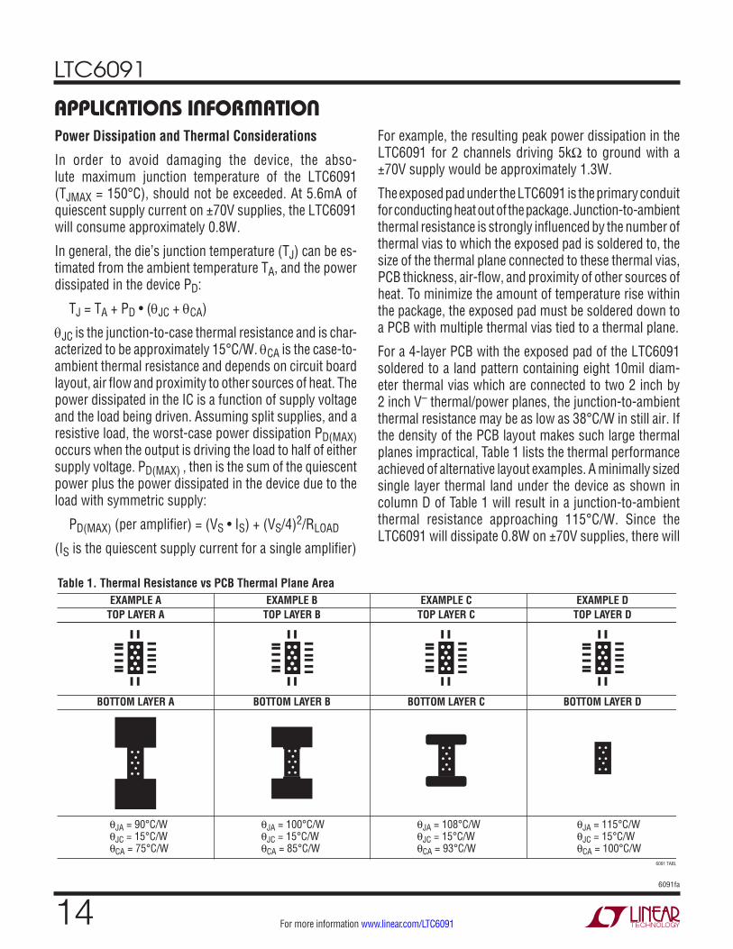
APPLICATIONS INFORMATIONPower Dissipation and Thermal Considerations
In order to avoid damaging the device, the abso-lute maximum junction temperature of the LTC6091 (TJMAX = 150°C), should not be exceeded. At 5.6mA of quiescent supply current on ±70V supplies, the LTC6091 will consume approximately 0.8W.
In general, the die’s junction temperature (TJ) can be es-timated from the ambient temperature TA, and the power dissipated in the device PD:
TJ = TA + PD • (θJC + θCA)
θJC is the junction-to-case thermal resistance and is char-acterized to be approximately 15°C/W. θCA is the case-to-ambient thermal resistance and depends on circuit board layout, air flow and proximity to other sources of heat. The power dissipated in the IC is a function of supply voltage and the load being driven. Assuming split supplies, and a resistive load, the worst-case power dissipation PD(MAX) occurs when the output is driving the load to half of either supply voltage. PD(MAX) , then is the sum of the quiescent power plus the power dissipated in the device due to the load with symmetric supply:
PD(MAX) (per amplifier) = (VS • IS) + (VS/4)2/RLOAD
(IS is the quiescent supply current for a single amplifier)
For example, the resulting peak power dissipation in the LTC6091 for 2 channels driving 5kΩ to ground with a ±70V supply would be approximately 1.3W.
The exposed pad under the LTC6091 is the primary conduit for conducting heat out of the package. Junction-to-ambient thermal resistance is strongly influenced by the number of thermal vias to which the exposed pad is soldered to, the size of the thermal plane connected to these thermal vias, PCB thickness, air-flow, and proximity of other sources of heat. To minimize the amount of temperature rise within the package, the exposed pad must be soldered down to a PCB with multiple thermal vias tied to a thermal plane.
For a 4-layer PCB with the exposed pad of the LTC6091 soldered to a land pattern containing eight 10mil diam-eter thermal vias which are connected to two 2 inch by 2 inch V– thermal/power planes, the junction-to-ambient thermal resistance may be as low as 38°C/W in still air. If the density of the PCB layout makes such large thermal planes impractical, Table 1 lists the thermal performance achieved of alternative layout examples. A minimally sized single layer thermal land under the device as shown in column D of Table 1 will result in a junction-to-ambient thermal resistance approaching 115°C/W. Since the LTC6091 will dissipate 0.8W on ±70V supplies, there will
TOP LAYER A TOP LAYER B TOP LAYER C TOP LAYER DEXAMPLE A EXAMPLE B EXAMPLE C EXAMPLE D
BOTTOM LAYER A
θJA = 90°C/WθJC = 15°C/WθCA = 75°C/W
θJA = 100°C/WθJC = 15°C/WθCA = 85°C/W
θJA = 108°C/WθJC = 15°C/WθCA = 93°C/W
θJA = 115°C/WθJC = 15°C/WθCA = 100°C/W
BOTTOM LAYER B BOTTOM LAYER C BOTTOM LAYER D
Table 1. Thermal Resistance vs PCB Thermal Plane Area
6091 TABLE 1
LTC6091
156091fa
For more information www.linear.com/LTC6091
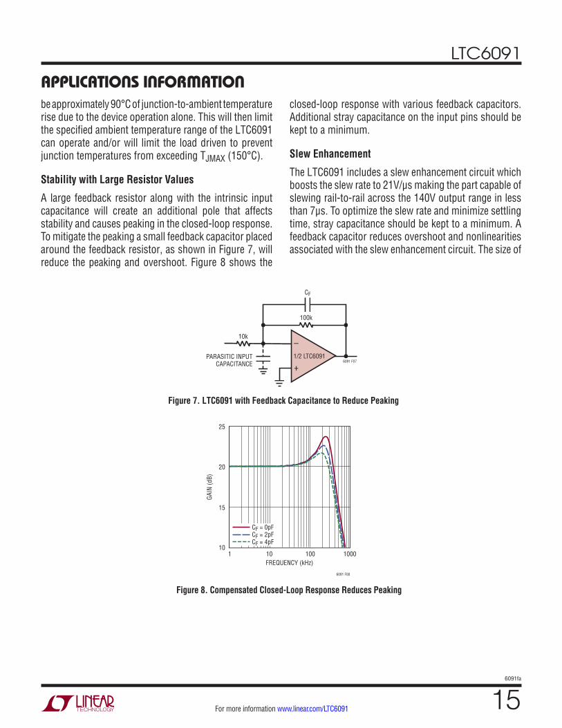
APPLICATIONS INFORMATION
Figure 7. LTC6091 with Feedback Capacitance to Reduce Peaking
6091 F07
–
+1/2 LTC6091
100k
CF
10k
PARASITIC INPUTCAPACITANCE
Figure 8. Compensated Closed-Loop Response Reduces Peaking
FREQUENCY (kHz)1
10
GAIN
(dB)
20
25
10 100 1000
6091 F08
15
CF = 0pFCF = 2pFCF = 4pF
be approximately 90°C of junction-to-ambient temperature rise due to the device operation alone. This will then limit the specified ambient temperature range of the LTC6091 can operate and/or will limit the load driven to prevent junction temperatures from exceeding TJMAX (150°C).
Stability with Large Resistor Values
A large feedback resistor along with the intrinsic input capacitance will create an additional pole that affects stability and causes peaking in the closed-loop response. To mitigate the peaking a small feedback capacitor placed around the feedback resistor, as shown in Figure 7, will reduce the peaking and overshoot. Figure 8 shows the
closed-loop response with various feedback capacitors. Additional stray capacitance on the input pins should be kept to a minimum.
Slew Enhancement
The LTC6091 includes a slew enhancement circuit which boosts the slew rate to 21V/μs making the part capable of slewing rail-to-rail across the 140V output range in less than 7μs. To optimize the slew rate and minimize settling time, stray capacitance should be kept to a minimum. A feedback capacitor reduces overshoot and nonlinearities associated with the slew enhancement circuit. The size of

LTC6091
166091fa
For more information www.linear.com/LTC6091
APPLICATIONS INFORMATIONthe feedback capacitor should be tailored to the specific board, supply voltage and load conditions.
Slewing is a nonlinear behavior and will affect distortion. The relationship between slew rate and full-power band-width is given in the relationship below.
SR = VPEAK • ω
where VPEAK is the peak output voltage and ω is frequency in radians/sec. The fidelity of a large sine wave output is limited by the slew rate. The graph in Figure 9 shows distortion versus frequency for several output levels.
Multiplexer Application
A single LTC6091 may be arranged to act as a 2-channel high voltage analog multiplexer as shown in Figure 10. When used in this arrangement, it is possible for the output to affect the source on the disabled amplifier’s noninverting input. The inverting and noninverting inputs are clamped through resistors and back-to-back diodes. There is a path for current to flow from the multiplexer output through the disabled amplifier’s feedback resistor, and through the inputs to the noninverting input’s source.
FREQUENCY (Hz)
TOTA
L HA
RMON
IC D
ISTO
RTIO
N +
NOIS
E (%
)
6091 F09
10
0.1
1
0.01
0.00110 100000100 1000 10000
VS = ±70VAV = 5RL = 10kCF = 30pF
VOUT = 100VP-P
VOUT = 50VP-P
VOUT = 10VP-P
Figure 9. Distortion vs Frequency for Large Output Swings
Figure 10. Multiplexer Application
6091 F10
CH110k OD
OD10k
10k 100k
10k 100k
CH2
SELECT
–
+
–
+1/2 LTC6091
1/2 LTC6091
COM
MUXOUT
COM
LTC6091
176091fa
For more information www.linear.com/LTC6091
APPLICATIONS INFORMATIONFor example, if the enabled amplifier has a –70V output, and the disabled amplifier has a 5V input, there is 75V across the two resistors and the input pins. To keep this current below 1mA the combined resistance of the RIN and feedback resistor needs to be about 75k or higher.
The output impedance of the disabled amplifier is > 10MΩ at DC. The AC output impedance is shown in the Typical Performance Characteristics section.
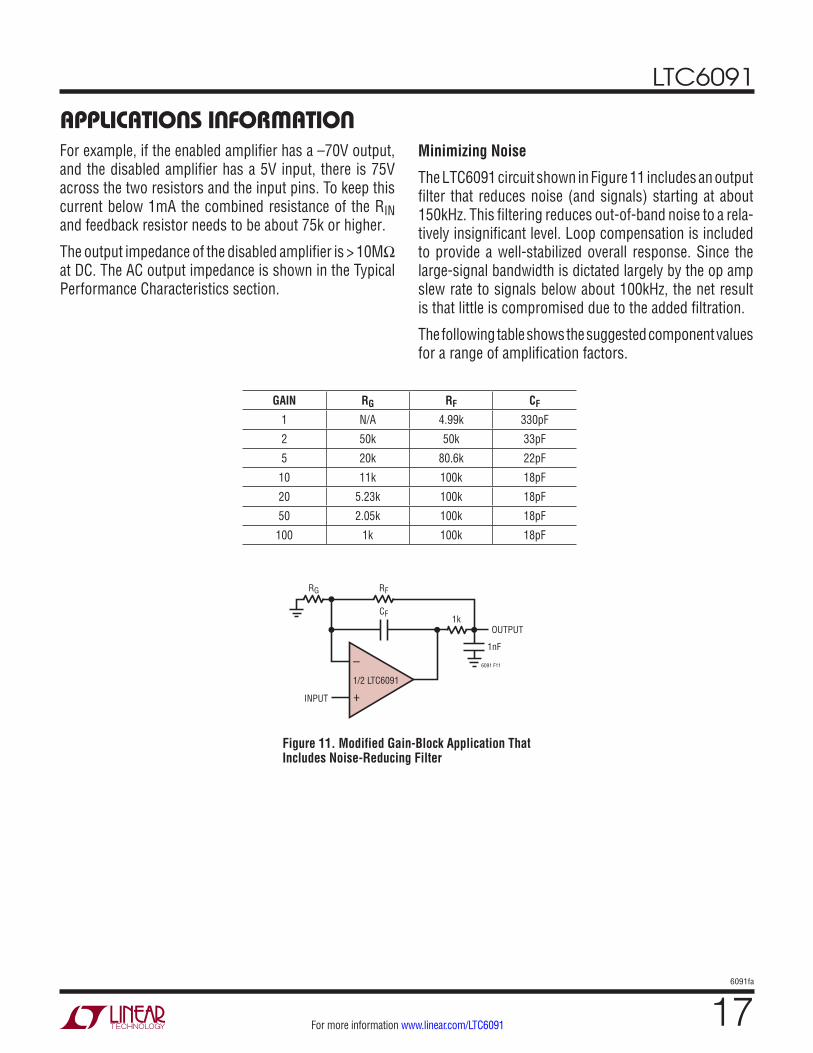
Figure 11. Modified Gain-Block Application That Includes Noise-Reducing Filter
CF
RF
1k
RG
OUTPUT
1nF
6091 F11
INPUT
–
+1/2 LTC6091
GAIN RG RF CF
1 N/A 4.99k 330pF
2 50k 50k 33pF
5 20k 80.6k 22pF
10 11k 100k 18pF
20 5.23k 100k 18pF
50 2.05k 100k 18pF
100 1k 100k 18pF
Minimizing Noise
The LTC6091 circuit shown in Figure 11 includes an output filter that reduces noise (and signals) starting at about 150kHz. This filtering reduces out-of-band noise to a rela-tively insignificant level. Loop compensation is included to provide a well-stabilized overall response. Since the large-signal bandwidth is dictated largely by the op amp slew rate to signals below about 100kHz, the net result is that little is compromised due to the added filtration.
The following table shows the suggested component values for a range of amplification factors.

LTC6091
186091fa
For more information www.linear.com/LTC6091
TYPICAL APPLICATIONSGain of 10 with Protected Output Current Doubler
Piezo Bimorph Bender Driver
6091 TA02
–
+1/2LTC6091
70V
–70V
200k1%
200k
12
15
22.1k1%
VIN
100Ω1%
–
+
70V
–70V
100Ω1%
±70VAT ±20mA
1/2LTC6091
16
8
11
4
–
+1/2 LTC6091
6091 TA03
10k
499Ω 7.5Ω
100k
IN±3V
317
16
1415
13
121
2
10k
–30V
30V
2SK1057
PHYSIK INSTRUMENTEPL140.10 (OR SIMILAR)MAX 4µF/LAYERfMAX = 500Hz
2SJ161
100k
2.2nF
100Ω
100Ω
LTC6091
196091fa
For more information www.linear.com/LTC6091
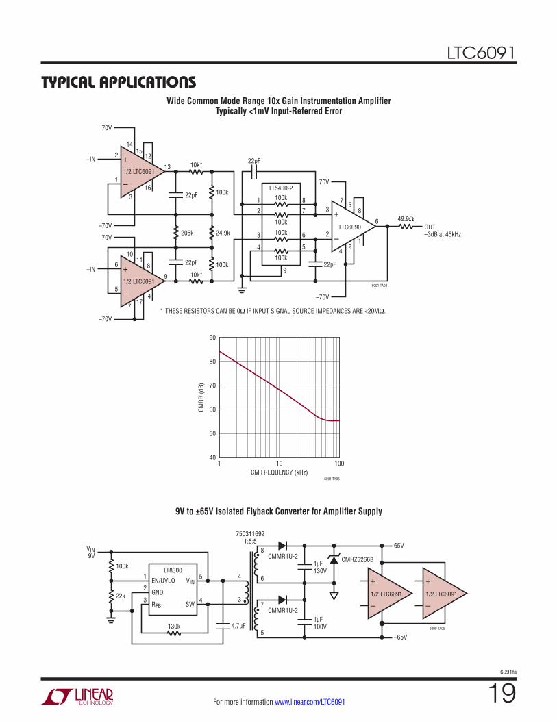
TYPICAL APPLICATIONSWide Common Mode Range 10x Gain Instrumentation Amplifier
Typically <1mV Input-Referred Error
+
–1/2 LTC6091
205k
10k*
22pF3
13
16
1415
122
1
+
–7
17
9
4
1011
86
5
24.9k
100k
100k
–70V
70V
–70V
70V
* THESE RESISTORS CAN BE 0Ω IF INPUT SIGNAL SOURCE IMPEDANCES ARE <20MΩ.
22pF
10k*
+
–LTC6090
100kLT5400-2
100k
100k
100k4
9
6
1
75
83
2
1
2
3
4
8
7
6
5
922pF
22pF+IN
–IN
70V
–70V
6091 TA04
49.9ΩOUT–3dB at 45kHz
1/2 LTC6091
CM FREQUENCY (kHz)
CMRR
(dB)
6091 TA05
90
40
50
60
70
80
1 10 100
6090 TA05
VIN9V
100k
22k
• CMMR1U-2
7503116921:5:5
CMMR1U-2 CMHZ5266B
1µF100V
1µF130V
+
–1/2 LTC6091
+
–1/2 LTC6091
65V
–65V
•
•
5
4
1
2
3
4.7µF
4
3
130k
EN/UVLO
GND
RFB
VIN
SW
LT8300
8
6
7
5
9V to ±65V Isolated Flyback Converter for Amplifier Supply

LTC6091
206091fa
For more information www.linear.com/LTC6091
Information furnished by Linear Technology Corporation is believed to be accurate and reliable. However, no responsibility is assumed for its use. Linear Technology Corporation makes no representa-tion that the interconnection of its circuits as described herein will not infringe on existing patent rights.
PACKAGE DESCRIPTIONPlease refer to http://www.linear.com/designtools/packaging/ for the most recent package drawings.
4.00 ±0.10
6.00 ±0.10
NOTE:1. DRAWING IS NOT A JEDEC PACKAGE OUTLINE2. DRAWING NOT TO SCALE3. ALL DIMENSIONS ARE IN MILLIMETERS4. DIMENSIONS OF EXPOSED PAD ON BOTTOM OF PACKAGE DO NOT INCLUDE MOLD FLASH. MOLD FLASH, IF PRESENT, SHALL NOT EXCEED 0.15mm ON ANY SIDE5. EXPOSED PAD SHALL BE SOLDER PLATED6. SHADED AREA IS ONLY A REFERENCE FOR PIN 1 LOCATION ON THE TOP AND BOTTOM OF PACKAGE
PIN 1TOP MARK(NOTE 6)
0.40 ±0.10
1615
1
2
9
14
78
BOTTOM VIEW—EXPOSED PAD
0.80BSC
0.75 ±0.05
PIN 1 NOTCHR = 0.30 OR0.35 × 45°CHAMFER
0.25 ±0.050.80 BSC
0.200 REF
0.00 – 0.05
(UFE32(16)) QFN 1113 REV O
RECOMMENDED SOLDER PAD PITCH AND DIMENSIONSAPPLY SOLDER MASK TO AREAS THAT ARE NOT SOLDERED
0.70 ±0.05
0.80 ±0.05
0.80 ±0.05
0.25 ±0.050.50 BSC
5.10 ±0.056.50 ±0.05
1.90 ±0.05
3.10 ±0.05
4.50 ±0.05
PACKAGE OUTLINE
1.90 ±0.10
4.10 ±0.10
4.10 ±0.05
UFE Package32(16)-Lead Plastic QFN (4mm × 6mm)(Reference LTC DWG # 05-08-1966 Rev O)
6
0.50 BSC
0.8BSC
0.8BSC
0.8BSC
0.50 BSC
0.50 BSC
0.80BSC
0.8BSC
0.8BSC
0.5BSC
0.5 BSC
0.8 BSC 0.8 BSC
0.8 BSC0.8 BSC0.8 BSC
0.8 BSC

LTC6091
216091fa
For more information www.linear.com/LTC6091
REVISION HISTORYREV DATE DESCRIPTION PAGE NUMBER
A 05/15 Removed ESD statement to reflect improved ESD PerformanceChanged internal TFLAG circuit resistor valuesUpdated Thermal Shutdown descriptionAdded pin numbers to application circuit
210, 11, 12
1218

LTC6091
226091fa
For more information www.linear.com/LTC6091 LINEAR TECHNOLOGY CORPORATION 2014
LT 0515 REV A• PRINTED IN USALinear Technology Corporation1630 McCarthy Blvd., Milpitas, CA 95035-7417(408) 432-1900 FAX: (408) 434-0507 www.linear.com/LTC6091
RELATED PARTS
TYPICAL APPLICATION
PART NUMBER DESCRIPTION COMMENTS
LTC6090 Single 140V Rail-to-Rail Output pA Input Op Amp Single Version of LTC6091
LT®1990 250V Input Range G = 1, 10, Micropower, Difference Amplifier Pin Selectable Gain of 1 or 10
LT1991 Precision, 100μA Gain Selectable Amplifier Pin Configurable as a Difference Amplifier, Inverting and Noninverting Amplifier
LT6015/LT6016/LT6017
Single/Dual/Quad 3.2MHz, Low Power, Over-The-Top® Precision Op Amp
76V Common Mode Input Range, 50V Operating Supply Range, 50μV Voltage Offset
LT3511 Monolithic High Voltage Isolated Flyback Converter 4.5V to 100V Input Voltage Range, No Opto-Coupler Required
LT8300 100VIN Micropower Isolated Flyback Converter with 150V/260mA Switch
6V to 100V Input Voltage Range. VOUT Set with a Single External Resistor
Piezo Micropositioner Driver
–
+1/2 LTC6091
6091 TA06
10k
499Ω330Ω
200k
IN+6V–1V
317
16
1415
13
121
2
10k
–20V
120V
2SK1057
2SJ161
200k
1nF
100Ω
100Ω
100Ω
100Ω
+120V–20V
CMAX = 10µFfMAX = 500Hz
PHYSIK INSTRUMENTEP-855 (OR SIMILAR)