Embed Size (px)
Citation preview

3V
0V
C001
A1 ±0.18 V
500mV 50�s
3V
0V
C002
A2 ±0.18 V
500mV 50�s
Product
Folder
Sample &Buy
Technical
Documents
Tools &
Software
Support &Community
LMC6482SNOS674E –NOVEMBER 1997–REVISED APRIL 2015
LMC6482 CMOS Dual Rail-to-Rail Input and Output Operational Amplifier1 Features 3 Description
The LMC6482 device provides a common-mode1• Typical Unless Otherwise Noted
range that extends to both supply rails. This rail-to-rail• Rail-to-Rail Input Common-Mode Voltage Range performance combined with excellent accuracy, due(Ensured Over Temperature) to a high CMRR, makes it unique among rail-to-rail
• Rail-to-Rail Output Swing (Within 20-mV of Supply input amplifiers. The device is ideal for systems, suchas data acquisition, that require a large input signalRail, 100-kΩ Load)range. The LMC6482 is also an excellent upgrade for• Ensured 3-V, 5-V, and 15-V Performancecircuits using limited common-mode range amplifiers
• Excellent CMRR and PSRR: 82 dB such as the TLC272 and TLC277.• Ultralow Input Current: 20 fA
Maximum dynamic signal range is assured in low• High Voltage Gain (R L = 500 k Ω): 130 dB voltage and single supply systems by the rail-to-rail• Specified for 2-kΩ and 600-Ω Loads output swing of the LMC6482. The rail-to-rail output
swing is ensured for loads down to 600 Ω of the• Power-Good Outputdevice. Ensured low-voltage characteristics and low-• Available in VSSOP Package power dissipation make the LMC6482 especially well-suited for battery-operated systems. LMC6482 is also2 Applications available in a VSSOP package, which is almost halfthe size of a SOIC-8 device. See the LMC6484 data• Data Acquisition Systemssheet for a quad CMOS operational amplifier with• Transducer Amplifiers these same features.
• Hand-held Analytic InstrumentsDevice Information(1)• Medical Instrumentation
PART NUMBER PACKAGE BODY SIZE (NOM)• Active Filter, Peak Detector, Sample and Hold, pHSOIC (8) 4.90 mm × 3.91 mmMeter, Current Source
LMC6482 VSSOP (8) 3.00 mm × 3.00 mm• Improved Replacement for TLC272, TLC277PDIP (8) 9.81 mm × 6.35 mm
(1) For all available packages, see the orderable addendum atthe end of the data sheet.
Rail-to-Rail Input Rail-to-Rail Output
1
An IMPORTANT NOTICE at the end of this data sheet addresses availability, warranty, changes, use in safety-critical applications,intellectual property matters and other important disclaimers. PRODUCTION DATA.

LMC6482SNOS674E –NOVEMBER 1997–REVISED APRIL 2015 www.ti.com
Table of Contents7.2 Functional Block Diagram ....................................... 181 Features .................................................................. 17.3 Feature Description................................................. 182 Applications ........................................................... 17.4 Device Functional Modes........................................ 193 Description ............................................................. 1
8 Application and Implementation ........................ 204 Revision History..................................................... 28.1 Application Information............................................ 205 Pin Configuration and Functions ......................... 38.2 Typical Applications ............................................... 226 Specifications......................................................... 3
9 Power Supply Recommendations ...................... 286.1 Absolute Maximum Ratings ...................................... 310 Layout................................................................... 286.2 ESD Ratings.............................................................. 4
10.1 Layout Guidelines ................................................. 286.3 Recommended Operating Conditions....................... 410.2 Layout Example .................................................... 286.4 Thermal Information .................................................. 4
11 Device and Documentation Support ................. 306.5 Electrical Characteristics for V+ = 5 V....................... 411.1 Trademarks ........................................................... 306.6 Electrical Characteristics for V+ = 3 V....................... 711.2 Electrostatic Discharge Caution............................ 306.7 Typical Characteristics .............................................. 911.3 Glossary ................................................................ 307 Detailed Description ............................................ 18
12 Mechanical, Packaging, and Orderable7.1 Overview ................................................................. 18Information ........................................................... 30
4 Revision HistoryNOTE: Page numbers for previous revisions may differ from page numbers in the current version.
Changes from Revision D (March 2013) to Revision E Page
• Added Pin Configuration and Functions section, ESD Ratings table, Feature Description section, Device FunctionalModes, Application and Implementation section, Power Supply Recommendations section, Layout section, Deviceand Documentation Support section, and Mechanical, Packaging, and Orderable Information section .............................. 1
Changes from Revision C (March 2013) to Revision D Page
• Changed layout of National Data Sheet to TI format ........................................................................................................... 27
2 Submit Documentation Feedback Copyright © 1997–2015, Texas Instruments Incorporated
Product Folder Links: LMC6482
LMC6482www.ti.com SNOS674E –NOVEMBER 1997–REVISED APRIL 2015
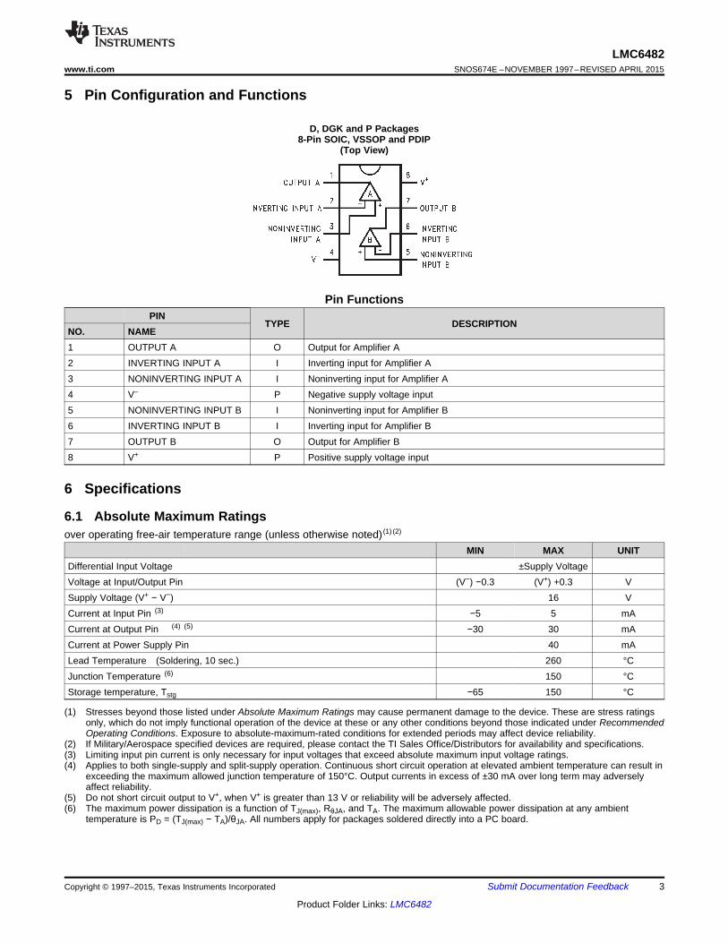
5 Pin Configuration and Functions
D, DGK and P Packages8-Pin SOIC, VSSOP and PDIP
(Top View)
Pin FunctionsPIN
TYPE DESCRIPTIONNO. NAME1 OUTPUT A O Output for Amplifier A2 INVERTING INPUT A I Inverting input for Amplifier A3 NONINVERTING INPUT A I Noninverting input for Amplifier A4 V– P Negative supply voltage input5 NONINVERTING INPUT B I Noninverting input for Amplifier B6 INVERTING INPUT B I Inverting input for Amplifier B7 OUTPUT B O Output for Amplifier B8 V+ P Positive supply voltage input
6 Specifications
6.1 Absolute Maximum Ratingsover operating free-air temperature range (unless otherwise noted) (1) (2)
MIN MAX UNITDifferential Input Voltage ±Supply VoltageVoltage at Input/Output Pin (V−) −0.3 (V+) +0.3 VSupply Voltage (V+ − V−) 16 VCurrent at Input Pin (3) −5 5 mACurrent at Output Pin (4) (5) −30 30 mACurrent at Power Supply Pin 40 mALead Temperature (Soldering, 10 sec.) 260 °CJunction Temperature (6) 150 °CStorage temperature, Tstg −65 150 °C
(1) Stresses beyond those listed under Absolute Maximum Ratings may cause permanent damage to the device. These are stress ratingsonly, which do not imply functional operation of the device at these or any other conditions beyond those indicated under RecommendedOperating Conditions. Exposure to absolute-maximum-rated conditions for extended periods may affect device reliability.
(2) If Military/Aerospace specified devices are required, please contact the TI Sales Office/Distributors for availability and specifications.(3) Limiting input pin current is only necessary for input voltages that exceed absolute maximum input voltage ratings.(4) Applies to both single-supply and split-supply operation. Continuous short circuit operation at elevated ambient temperature can result in
exceeding the maximum allowed junction temperature of 150°C. Output currents in excess of ±30 mA over long term may adverselyaffect reliability.
(5) Do not short circuit output to V+, when V+ is greater than 13 V or reliability will be adversely affected.(6) The maximum power dissipation is a function of TJ(max), RθJA, and TA. The maximum allowable power dissipation at any ambient
temperature is PD = (TJ(max) − TA)/θJA. All numbers apply for packages soldered directly into a PC board.
Copyright © 1997–2015, Texas Instruments Incorporated Submit Documentation Feedback 3
Product Folder Links: LMC6482

LMC6482SNOS674E –NOVEMBER 1997–REVISED APRIL 2015 www.ti.com
6.2 ESD RatingsVALUE UNIT
V(ESD) Electrostatic discharge Human-body model (HBM), per ANSI/ESDA/JEDEC JS-001 (1) ±1500 V
(1) JEDEC document JEP155 states that 500-V HBM allows safe manufacturing with a standard ESD control process.
6.3 Recommended Operating Conditionsover operating free-air temperature range (unless otherwise noted) (1)
MIN MAX UNITSupply Voltage 3 15.5 V
LMC6482AM –55 125 °CJunction Temperature Range
LMC6482AI, LMC6482I –40 −85 °C
(1) Stresses beyond those listed under Absolute Maximum Ratings may cause permanent damage to the device. These are stress ratingsonly, which do not imply functional operation of the device at these or any other conditions beyond those indicated under RecommendedOperating Conditions. Exposure to absolute-maximum-rated conditions for extended periods may affect device reliability.
6.4 Thermal InformationLMC6482 LMC6482 LMC6482
THERMAL METRIC (1) D (SOIC) DGK (VSSOP) P (PDIP) UNIT8 PINS 8 PINS 8 PINS
RθJA Junction-to-ambient thermal resistance 155 194 90 °C/W
(1) For more information about traditional and new thermal metrics, see the IC Package Thermal Metrics application report, SPRA953.
6.5 Electrical Characteristics for V+ = 5 VUnless otherwise specified, all limits specified for TJ = 25°C, V+ = 5 V, V− = 0 V, VCM = VO = V+/2 and RL > 1 M.
At TemperatureTJ = 25°C Extremes (1)PARAMETER TEST CONDITIONS UNITMIN TYP (2) MAX (3) MIN TYP (2) MAX (3)
DC Electrical CharacteristicsLMC6482AI 0.11 0.75 1.35
Input OffsetVOS LMC6482I 0.11 3 3.7 mVVoltageLMC6482M 0.11 3 3.8
TCVOS Input Offset 1Voltage μV/°CAverage Drift
LMC6482AI 0.02 4IB Input Current See (4) LMC6482I 0.02 4 pA
LMC6482M 0.02 10LMC6482AI 0.01 2
Input OffsetIOS See (4) LMC6482I 0.01 2 pACurrentLMC6482M 0.01 5
CIN Common- 3Mode Input pFCapacitance
RIN Input 10 TeraΩResistance
(1) See Recommended Operating Conditions for operating temperature ranges.(2) Typical Values represent the most likely parametric norm.(3) All limits are specified by testing or statistical analysis.(4) Ensured limits are dictated by tester limitations and not device performance. Actual performance is reflected in the typical value.
4 Submit Documentation Feedback Copyright © 1997–2015, Texas Instruments Incorporated
Product Folder Links: LMC6482

LMC6482www.ti.com SNOS674E –NOVEMBER 1997–REVISED APRIL 2015
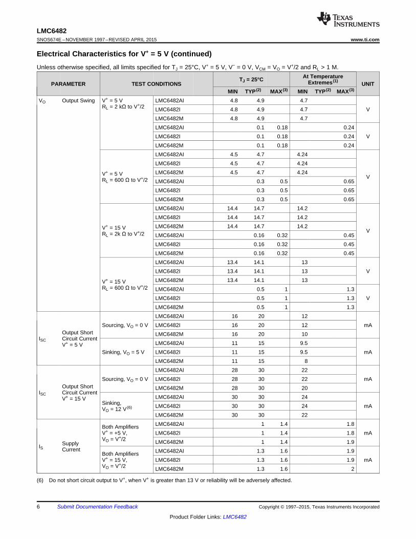
Electrical Characteristics for V+ = 5 V (continued)Unless otherwise specified, all limits specified for TJ = 25°C, V+ = 5 V, V− = 0 V, VCM = VO = V+/2 and RL > 1 M.
At TemperatureTJ = 25°C Extremes (1)PARAMETER TEST CONDITIONS UNITMIN TYP (2) MAX (3) MIN TYP (2) MAX (3)
LMC6482AI 70 82 670 V ≤ VCM ≤ 15 V LMC6482I 65 82 62V+ = 15 VCommon-
LMC6482M 65 82 60ModeCMRR dBRejection LMC6482AI 70 82 67Ratio 0 V ≤ VCM ≤ 5 V LMC6482I 65 82 62V+ = 5 V
LMC6482M 65 82 60Positive LMC6482AI 70 82 675 V ≤ V+ ≤ 15 V,Power Supply LMC6482I 65 82 62+PSRR V− = 0 V dBRejection VO = 2.5 V LMC6482M 65 82 60RatioNegative LMC6482AI 70 82 67−5 V ≤ V− ≤ −15 V,Power Supply LMC6482I 65 82 62−PSRR V+ = 0 V dBRejection VO = −2.5 V LMC6482M 65 82 60Ratio
LMC6482AI V− − 0.3 −0.25 0LMC6482I V− − 0.3 −0.25 0 VLMC6482M V− − 0.3 −0.25 0
InputLMC6482AI V+ + V+ + 0.3 V+
Common- V+ = 5 V and 15 VVCM 0.25Mode Voltage For CMRR ≥ 50 dBRange LMC6482I V+ + V+ + 0.3 V+
V0.25LMC6482M V+ + V+ + 0.3 V+
0.25LMC6482AI 140 666 84
Sourcing LMC6482I 120 666 72 V/mVLMC6482M 120 666 60
RL = 2 kΩ (5) (4)LMC6482AI 35 75 20
Sinking LMC6482I 35 75 20 V/mVLMC6482M 35 75 18Large SignalAV Voltage Gain LMC6482AI 80 300 48
Sourcing LMC6482I 50 300 30 V/mVLMC6482M 50 300 25
RL = 600 Ω (5) (4)LMC6482AI 20 35 13
Sinking LMC6482I 15 35 10 V/mVLMC6482M 15 35 8
(5) V+ = 15 V, VCM = 7.5 V and RL connected to 7.5 V. For Sourcing tests, 7.5 V ≤ VO ≤ 11.5 V. For Sinking tests, 3.5 V ≤ VO ≤ 7.5 V.
Copyright © 1997–2015, Texas Instruments Incorporated Submit Documentation Feedback 5
Product Folder Links: LMC6482
LMC6482SNOS674E –NOVEMBER 1997–REVISED APRIL 2015 www.ti.com
Electrical Characteristics for V+ = 5 V (continued)Unless otherwise specified, all limits specified for TJ = 25°C, V+ = 5 V, V− = 0 V, VCM = VO = V+/2 and RL > 1 M.
At TemperatureTJ = 25°C Extremes (1)PARAMETER TEST CONDITIONS UNITMIN TYP (2) MAX (3) MIN TYP (2) MAX (3)
VO Output Swing V+ = 5 V LMC6482AI 4.8 4.9 4.7RL = 2 kΩ to V+/2 LMC6482I 4.8 4.9 4.7 V
LMC6482M 4.8 4.9 4.7LMC6482AI 0.1 0.18 0.24LMC6482I 0.1 0.18 0.24 VLMC6482M 0.1 0.18 0.24LMC6482AI 4.5 4.7 4.24LMC6482I 4.5 4.7 4.24LMC6482M 4.5 4.7 4.24V+ = 5 V VRL = 600 Ω to V+/2 LMC6482AI 0.3 0.5 0.65LMC6482I 0.3 0.5 0.65LMC6482M 0.3 0.5 0.65LMC6482AI 14.4 14.7 14.2LMC6482I 14.4 14.7 14.2LMC6482M 14.4 14.7 14.2V+ = 15 V VRL = 2k Ω to V+/2 LMC6482AI 0.16 0.32 0.45LMC6482I 0.16 0.32 0.45LMC6482M 0.16 0.32 0.45LMC6482AI 13.4 14.1 13LMC6482I 13.4 14.1 13 VLMC6482M 13.4 14.1 13V+ = 15 V
RL = 600 Ω to V+/2 LMC6482AI 0.5 1 1.3LMC6482I 0.5 1 1.3 VLMC6482M 0.5 1 1.3LMC6482AI 16 20 12
Sourcing, VO = 0 V LMC6482I 16 20 12 mAOutput Short LMC6482M 16 20 10
ISC Circuit CurrentLMC6482AI 11 15 9.5V+ = 5 V
Sinking, VO = 5 V LMC6482I 11 15 9.5 mALMC6482M 11 15 8LMC6482AI 28 30 22
Sourcing, VO = 0 V LMC6482I 28 30 22 mAOutput Short LMC6482M 28 30 20
ISC Circuit CurrentLMC6482AI 30 30 24V+ = 15 V
Sinking, LMC6482I 30 30 24 mAVO = 12 V (6)
LMC6482M 30 30 22LMC6482AI 1 1.4 1.8Both Amplifiers
V+ = +5 V, LMC6482I 1 1.4 1.8 mAVO = V+/2 LMC6482M 1 1.4 1.9SupplyIS Current LMC6482AI 1.3 1.6 1.9Both AmplifiersV+ = 15 V, LMC6482I 1.3 1.6 1.9 mAVO = V+/2 LMC6482M 1.3 1.6 2
(6) Do not short circuit output to V+, when V+ is greater than 13 V or reliability will be adversely affected.
6 Submit Documentation Feedback Copyright © 1997–2015, Texas Instruments Incorporated
Product Folder Links: LMC6482

LMC6482www.ti.com SNOS674E –NOVEMBER 1997–REVISED APRIL 2015
Electrical Characteristics for V+ = 5 V (continued)Unless otherwise specified, all limits specified for TJ = 25°C, V+ = 5 V, V− = 0 V, VCM = VO = V+/2 and RL > 1 M.
At TemperatureTJ = 25°C Extremes (1)PARAMETER TEST CONDITIONS UNITMIN TYP (2) MAX (3) MIN TYP (2) MAX (3)
AC Electrical CharacteristicsSee (7) LMC6482AI 1 1.3 0.7
V/μsSR Slew Rate LMC6482I 0.9 1.3 0.63
LMC6482M 0.9 1.3 0.54 V/μsGain- V+ = 15 V
GBW Bandwidth 1.5 MHzProduct
φm Phase Margin 50 DegGm Gain Margin 15 dB
Amp-to-Amp See (8)150 dBIsolation
Input-Referred F = 1 kHzen 37 nV/√HzVoltage Noise Vcm = 1 VInput-Referred F = 1 kHzIn 0.03 pA/√HzCurrent Noise
F = 10 kHz, AV = −2RL = 10 kΩ, 0.01%VO = 4.1 VPPTotal
T.H.D. Harmonic F = 10 kHz, AV = −2Distortion RL = 10 kΩ, 0.01%VO = 8.5 VPP
V+ = 10 V
(7) V + = 15V. Connected as Voltage Follower with 10V step input. Number specified is the slower of either the positive or negative slewrates.
(8) Input referred, V+ = 15 V and RL = 100 kΩ connected to 7.5 V. Each amp excited in turn with 1 kHz to produce VO = 12 VPP.
6.6 Electrical Characteristics for V+ = 3 VUnless otherwise specified, all limits specified for TJ = 25°C, V+ = 3V, V− = 0V, VCM = VO = V+/2 and RL > 1M.
At TemperatureTJ = 25°C Extremes (1)PARAMETER TEST CONDITIONS UNITMIN TYP (2) MAX (3) MIN TYP (2) MAX (3)
DC Electrical CharacteristicsLMC6482AI 0.9 2 2.7
Input OffsetVOS LMC6482I 0.9 3 3.7 mVVoltageLMC6482M 0.9 3 3.8
Input OffsetTCVOS Voltage 2 μV/°C
Average DriftInput Bias 0.02IB pACurrentInput Offset 0.01IOS pACurrentCommon LMC6482AI 64 74Mode LMC6482I 60 74CMRR 0 V ≤ VCM ≤ 3 V dBRejection
LMC6482M 60 74Ratio
(1) See Recommended Operating Conditions for operating temperature ranges.(2) Typical Values represent the most likely parametric norm.(3) All limits are specified by testing or statistical analysis.
Copyright © 1997–2015, Texas Instruments Incorporated Submit Documentation Feedback 7
Product Folder Links: LMC6482

LMC6482SNOS674E –NOVEMBER 1997–REVISED APRIL 2015 www.ti.com
Electrical Characteristics for V+ = 3 V (continued)Unless otherwise specified, all limits specified for TJ = 25°C, V+ = 3V, V− = 0V, VCM = VO = V+/2 and RL > 1M.
At TemperatureTJ = 25°C Extremes (1)PARAMETER TEST CONDITIONS UNITMIN TYP (2) MAX (3) MIN TYP (2) MAX (3)
LMC6482AI 68 80Power Supply 3 V ≤ V+ ≤ 15 V,PSRR Rejection LMC6482I 60 80 dBV− = 0 VRatio LMC6482M 60 80LMC6482AI V− −0.25 0LMC6482I V− −0.25 0 V
InputLMC6482M V− −0.25 0Common- For CMRR ≥ 50VCM Mode Voltage dB LMC6482AI V+ V+ + 0.25
RangeLMC6482I V+ V+ + 0.25 VLMC6482M V+ V+ + 0.25
2.8 VRL = 2 kΩ to V+/2
0.2 VLMC6482AI 2.5 2.7LMC6482I 2.5 2.7 V
VO Output SwingLMC6482M 2.5 2.7RL = 600 Ω to
V+/2 LMC6482AI 0.37 0.6LMC6482I 0.37 0.6 VLMC6482M 0.37 0.6LMC6482AI 0.825 1.2 1.5
IS Supply Current Both Amplifiers LMC6482I 0.825 1.2 1.5 mALMC6482M 0.825 1.2 1.6
AC Electrical CharacteristicsSR Slew Rate See (4) 0.9 V/μs
Gain- 1 MHzGBW Bandwidth
ProductTotal F = 10 kHz, AV = −2
T.H.D. Harmonic RL = 10 kΩ, VO = 2 VPP 0.01%Distortion
(4) Connected as voltage Follower with 2-V step input. Number specified is the slower of either the positive or negative slew rates.
8 Submit Documentation Feedback Copyright © 1997–2015, Texas Instruments Incorporated
Product Folder Links: LMC6482

LMC6482www.ti.com SNOS674E –NOVEMBER 1997–REVISED APRIL 2015
6.7 Typical CharacteristicsVS = 15 V, Single Supply, TA = 25°C unless otherwise specified
Figure 1. Supply Current vs. Supply Voltage Figure 2. Input Current vs. Temperature
Figure 3. Sourcing Current vs. Output Voltage Figure 4. Sourcing Current vs. Output Voltage
Figure 6. Sinking Current vs. Output VoltageFigure 5. Sourcing Current vs. Output Voltage
Copyright © 1997–2015, Texas Instruments Incorporated Submit Documentation Feedback 9
Product Folder Links: LMC6482

LMC6482SNOS674E –NOVEMBER 1997–REVISED APRIL 2015 www.ti.com
Typical Characteristics (continued)VS = 15 V, Single Supply, TA = 25°C unless otherwise specified
Figure 7. Sinking Current vs. Output Voltage Figure 8. Sinking Current vs. Output Voltage
Figure 10. Input Voltage Noise vs. FrequencyFigure 9. Output Voltage Swing vs. Supply Voltage
Figure 11. Input Voltage Noise vs. Input Voltage Figure 12. Input Voltage Noise vs. Input Voltage
10 Submit Documentation Feedback Copyright © 1997–2015, Texas Instruments Incorporated
Product Folder Links: LMC6482

LMC6482www.ti.com SNOS674E –NOVEMBER 1997–REVISED APRIL 2015
Typical Characteristics (continued)VS = 15 V, Single Supply, TA = 25°C unless otherwise specified
Figure 13. Input Voltage Noise vs. Input Voltage Figure 14. Crosstalk Rejection vs. Frequency
Figure 15. Crosstalk Rejection vs. Frequency Figure 16. Positive PSRR vs. Frequency
Figure 17. Negative PSRR vs. Frequency Figure 18. CMRR vs. Frequency
Copyright © 1997–2015, Texas Instruments Incorporated Submit Documentation Feedback 11
Product Folder Links: LMC6482

LMC6482SNOS674E –NOVEMBER 1997–REVISED APRIL 2015 www.ti.com
Typical Characteristics (continued)VS = 15 V, Single Supply, TA = 25°C unless otherwise specified
Figure 19. CMRR vs. Input Voltage Figure 20. CMRR vs. Input Voltage
Figure 21. CMRR vs. Input Voltage Figure 22. ΔvOS vs. CMR
Figure 24. Input Voltage vs. Output VoltageFigure 23. ΔvOS vs. CMR
12 Submit Documentation Feedback Copyright © 1997–2015, Texas Instruments Incorporated
Product Folder Links: LMC6482

LMC6482www.ti.com SNOS674E –NOVEMBER 1997–REVISED APRIL 2015
Typical Characteristics (continued)VS = 15 V, Single Supply, TA = 25°C unless otherwise specified
Figure 25. Input Voltage vs. Output Voltage Figure 26. Open-Loop Frequency Response
Figure 27. Open-Loop Frequency Response Figure 28. Open-Loop Frequency Response vs. Temperature
Figure 29. Maximum Output Swing vs. Frequency Figure 30. Gain and Phase vs. Capacitive Load
Copyright © 1997–2015, Texas Instruments Incorporated Submit Documentation Feedback 13
Product Folder Links: LMC6482

LMC6482SNOS674E –NOVEMBER 1997–REVISED APRIL 2015 www.ti.com
Typical Characteristics (continued)VS = 15 V, Single Supply, TA = 25°C unless otherwise specified
Figure 31. Gain and Phase vs. Capacitive Load Figure 32. Open-Loop Output Impedance vs. Frequency
Figure 34. Slew Rate vs. Supply VoltageFigure 33. Open-Loop Output Impedance vs. Frequency
Figure 35. Noninverting Large Signal Pulse Response Figure 36. Noninverting Large Signal Pulse Response
14 Submit Documentation Feedback Copyright © 1997–2015, Texas Instruments Incorporated
Product Folder Links: LMC6482

LMC6482www.ti.com SNOS674E –NOVEMBER 1997–REVISED APRIL 2015
Typical Characteristics (continued)VS = 15 V, Single Supply, TA = 25°C unless otherwise specified
Figure 37. Noninverting Large Signal Pulse Response Figure 38. Noninverting Small Signal Pulse Response
Figure 39. Noninverting Small Signal Pulse Response Figure 40. Noninverting Small Signal Pulse Response
Figure 41. Inverting Large Signal Pulse Response Figure 42. Inverting Large Signal Pulse Response
Copyright © 1997–2015, Texas Instruments Incorporated Submit Documentation Feedback 15
Product Folder Links: LMC6482

LMC6482SNOS674E –NOVEMBER 1997–REVISED APRIL 2015 www.ti.com
Typical Characteristics (continued)VS = 15 V, Single Supply, TA = 25°C unless otherwise specified
Figure 43. Inverting Large Signal Pulse Response Figure 44. Inverting Small Signal Pulse Response
Figure 45. Inverting Small Signal Pulse Response Figure 46. Inverting Small Signal Pulse Response
Figure 47. Stability vs. Capacitive Load Figure 48. Stability vs. Capacitive Load
16 Submit Documentation Feedback Copyright © 1997–2015, Texas Instruments Incorporated
Product Folder Links: LMC6482

LMC6482www.ti.com SNOS674E –NOVEMBER 1997–REVISED APRIL 2015
Typical Characteristics (continued)VS = 15 V, Single Supply, TA = 25°C unless otherwise specified
Figure 49. Stability vs. Capacitive Load Figure 50. Stability vs. Capacitive Load
Figure 51. Stability vs. Capacitive Load Figure 52. Stability vs. Capacitive Load
Copyright © 1997–2015, Texas Instruments Incorporated Submit Documentation Feedback 17
Product Folder Links: LMC6482
LMC6482SNOS674E –NOVEMBER 1997–REVISED APRIL 2015 www.ti.com
7 Detailed Description
7.1 OverviewThe LMC6482 is a dual CMOS operational amplifier that supports both rail-to-rail inputs and outputs. It may beoperated in both dual supply mode and single supply mode.
7.2 Functional Block Diagram
7.3 Feature Description
7.3.1 Amplifier TopologyThe LMC6482 incorporates specially designed wide-compliance range current mirrors and the body effect toextend input common-mode range to each supply rail. Complementary paralleled differential input stages, like thetype used in other CMOS and bipolar rail-to-rail input amplifiers, were not used because of their inherentaccuracy problems due to CMRR, crossover distortion, and open-loop gain variation.
The LMC6482s input stage design is complemented by an output stage capable of rail-to-rail output swing evenwhen driving a large load. Rail-to-rail output swing is obtained by taking the output directly from the internalintegrator instead of an output buffer stage.
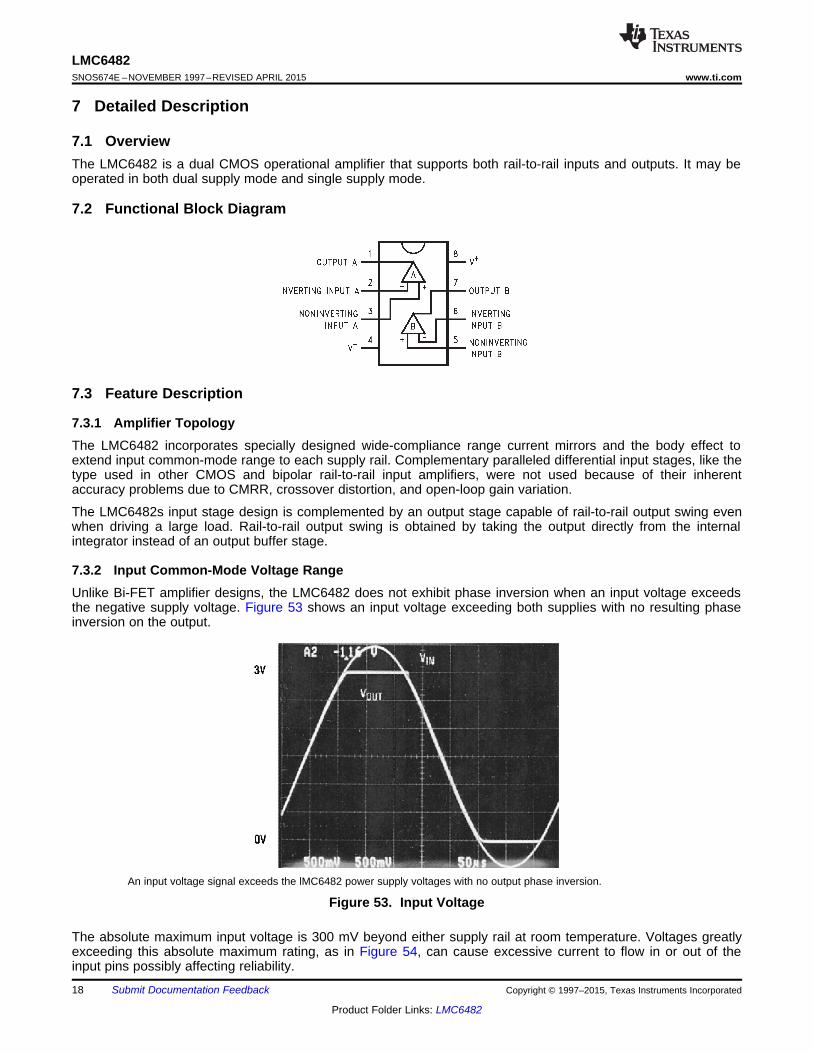
7.3.2 Input Common-Mode Voltage RangeUnlike Bi-FET amplifier designs, the LMC6482 does not exhibit phase inversion when an input voltage exceedsthe negative supply voltage. Figure 53 shows an input voltage exceeding both supplies with no resulting phaseinversion on the output.
An input voltage signal exceeds the lMC6482 power supply voltages with no output phase inversion.
Figure 53. Input Voltage
The absolute maximum input voltage is 300 mV beyond either supply rail at room temperature. Voltages greatlyexceeding this absolute maximum rating, as in Figure 54, can cause excessive current to flow in or out of theinput pins possibly affecting reliability.
18 Submit Documentation Feedback Copyright © 1997–2015, Texas Instruments Incorporated
Product Folder Links: LMC6482

LMC6482www.ti.com SNOS674E –NOVEMBER 1997–REVISED APRIL 2015
Feature Description (continued)
A ±7.5-V input signal greatly exceeds the 3-V supply in Figure 55 causing no phase inversion due to RI.
Figure 54. Input Signal
Applications that exceed this rating must externally limit the maximum input current to ±5 mA with an inputresistor (RI) as shown in Figure 55.
RI input current protection for voltages exceeding the supply voltages.
Figure 55. RI Input Current Protection forVoltages Exceeding the Supply Voltages
7.3.3 Rail-to-Rail OutputThe approximated output resistance of the LMC6482 is 180-Ω sourcing and 13-0Ω sinking at VS = 3 V and 110-Ωsourcing and 80-Ω sinking at Vs = 5 V. Using the calculated output resistance, maximum output voltage swingcan be estimated as a function of load.
7.4 Device Functional ModesThe LMC6482 may be used in applications where each amplifier channel is used independently, or inapplications in which the channels are cascaded. See Typical Applications for more information.
Copyright © 1997–2015, Texas Instruments Incorporated Submit Documentation Feedback 19
Product Folder Links: LMC6482
LMC6482SNOS674E –NOVEMBER 1997–REVISED APRIL 2015 www.ti.com
8 Application and Implementation
NOTEInformation in the following applications sections is not part of the TI componentspecification, and TI does not warrant its accuracy or completeness. TI’s customers areresponsible for determining suitability of components for their purposes. Customers shouldvalidate and test their design implementation to confirm system functionality.
8.1 Application Information
8.1.1 Upgrading ApplicationsThe LMC6484 quads and LMC6482 duals have industry-standard pin outs to retrofit existing applications.System performance can be greatly increased by the features of the LMC6482. The key benefit of designing inthe LMC6482 is increased linear signal range. Most op-amps have limited input common-mode ranges. Signalsthat exceed this range generate a nonlinear output response that persists long after the input signal returns tothe common-mode range.
Linear signal range is vital in applications such as filters where signal peaking can exceed input common-moderanges resulting in output phase inversion or severe distortion.
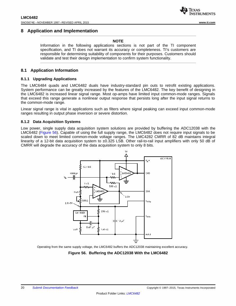
8.1.2 Data Acquisition SystemsLow power, single supply data acquisition system solutions are provided by buffering the ADC12038 with theLMC6482 (Figure 56). Capable of using the full supply range, the LMC6482 does not require input signals to bescaled down to meet limited common-mode voltage ranges. The LMC4282 CMRR of 82 dB maintains integrallinearity of a 12-bit data acquisition system to ±0.325 LSB. Other rail-to-rail input amplifiers with only 50 dB ofCMRR will degrade the accuracy of the data acquisition system to only 8 bits.
Operating from the same supply voltage, the LMC6482 buffers the ADC12038 maintaining excellent accuracy.
Figure 56. Buffering the ADC12038 With the LMC6482
20 Submit Documentation Feedback Copyright © 1997–2015, Texas Instruments Incorporated
Product Folder Links: LMC6482

LMC6482www.ti.com SNOS674E –NOVEMBER 1997–REVISED APRIL 2015
Application Information (continued)8.1.3 Instrumentation CircuitsThe LMC6482 has the high input impedance, large common-mode range and high CMRR needed for designinginstrumentation circuits. Instrumentation circuits designed with the LMC6482 can reject a larger range ofcommon-mode signals than most in-amps. This makes instrumentation circuits designed with the LMC6482 anexcellent choice of noisy or industrial environments. Other applications that benefit from these features includeanalytic medical instruments, magnetic field detectors, gas detectors, and silicon-based transducers.
A small valued potentiometer is used in series with Rg to set the differential gain of the 3-op-amp instrumentationcircuit in Figure 57. This combination is used instead of one large valued potentiometer to increase gain trimaccuracy and reduce error due to vibration.
Figure 57. Low Power 3-Op-Amp Instrumentation Amplifier
A 2-op-amp instrumentation amplifier designed for a gain of 100 is shown in Figure 58. Low sensitivity trimmingis made for offset voltage, CMRR, and gain. Low cost and low power consumption are the main advantages ofthis 2-op-amp circuit.
Higher frequency and larger common-mode range applications are best facilitated by a 3-op-amp instrumentationamplifier.
Figure 58. Low-Power Two-Op-Amp Instrumentation Amplifier
8.1.4 Spice MacromodelA spice macromodel is available for the LMC6482. This model includes accurate simulation of the following:• Input common-mode voltage range• Frequency and transient response• GBW dependence on loading conditions• Quiescent and dynamic supply current• Output swing dependence on loading conditions
Many more characteristics are listed on the macromodel disk.
Copyright © 1997–2015, Texas Instruments Incorporated Submit Documentation Feedback 21
Product Folder Links: LMC6482

LMC6482SNOS674E –NOVEMBER 1997–REVISED APRIL 2015 www.ti.com
Application Information (continued)Contact your local TI sales office to obtain an operational amplifier spice model library disk.
8.2 Typical Applications
8.2.1 3-V Single Supply Buffer Circuit
Figure 59. 3-V Single Supply Buffer Circuit
8.2.1.1 Design RequirementsFor best performance, ensure that the input voltage swing is between V+ and V-.
Ensure that the input does not exceed the common-mode input range.
To reduce the risk of destabilizing the output, use resistive isolation on the output when driving capacitive loads(see the Detailed Design Procedure section).
When large feedback resistors are used, it may be necessary to compensate for parasitic capacitance on theinput. See the Detailed Design Procedure section.
8.2.1.2 Detailed Design Procedure
8.2.1.2.1 Capacitive Load Compensation
Capacitive load compensation can be accomplished using resistive isolation as shown in Figure 60. This simpletechnique is useful for isolating the capacitive inputs of multiplexers and A/D converters.
Figure 60. Resistive Isolation of a 330-pF Capacitive Load
Figure 61. Pulse Response of the LMC6482 Circuit in Figure 60
22 Submit Documentation Feedback Copyright © 1997–2015, Texas Instruments Incorporated
Product Folder Links: LMC6482
LMC6482www.ti.com SNOS674E –NOVEMBER 1997–REVISED APRIL 2015
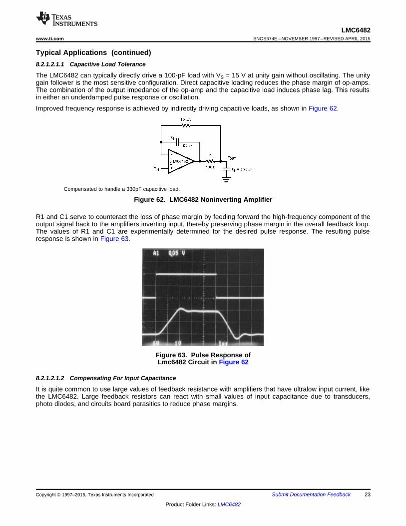
Typical Applications (continued)8.2.1.2.1.1 Capacitive Load Tolerance
The LMC6482 can typically directly drive a 100-pF load with VS = 15 V at unity gain without oscillating. The unitygain follower is the most sensitive configuration. Direct capacitive loading reduces the phase margin of op-amps.The combination of the output impedance of the op-amp and the capacitive load induces phase lag. This resultsin either an underdamped pulse response or oscillation.
Improved frequency response is achieved by indirectly driving capacitive loads, as shown in Figure 62.
Compensated to handle a 330pF capacitive load.
Figure 62. LMC6482 Noninverting Amplifier
R1 and C1 serve to counteract the loss of phase margin by feeding forward the high-frequency component of theoutput signal back to the amplifiers inverting input, thereby preserving phase margin in the overall feedback loop.The values of R1 and C1 are experimentally determined for the desired pulse response. The resulting pulseresponse is shown in Figure 63.
Figure 63. Pulse Response ofLmc6482 Circuit in Figure 62
8.2.1.2.1.2 Compensating For Input Capacitance
It is quite common to use large values of feedback resistance with amplifiers that have ultralow input current, likethe LMC6482. Large feedback resistors can react with small values of input capacitance due to transducers,photo diodes, and circuits board parasitics to reduce phase margins.
Copyright © 1997–2015, Texas Instruments Incorporated Submit Documentation Feedback 23
Product Folder Links: LMC6482

VIN
VOUT
+
-
5V
-5V
R4
R3
V-
1
2LMC6482
V-
V+
500 k:
1 k:
500 k:
499:
1 M:
VOUT
VIN= -
R4R3
LMC6482SNOS674E –NOVEMBER 1997–REVISED APRIL 2015 www.ti.com
Typical Applications (continued)
Figure 64. Canceling the Effect of Input Capacitance
The effect of input capacitance can be compensated for by adding a feedback capacitor. The feedback capacitor(as in Figure 64), Cf, is first estimated by:
(1)
orR1 CIN ≤ R2 Cf (2)
which typically provides significant overcompensation.
Printed-circuit-board stray capacitance may be larger or smaller than that of a bread-board, so the actualoptimum value for Cf may be different. The values of Cf should be checked on the actual circuit. (Refer to theLMC660 quad CMOS amplifier data sheet for a more detailed discussion.)
8.2.1.2.1.3 Offset Voltage Adjustment
Offset voltage adjustment circuits are illustrated in Figure 65 and Figure 66. Large value resistances andpotentiometers are used to reduce power consumption while providing typically ±2.5 mV of adjustment range,referred to the input, for both configurations with VS = ±5 V.
Figure 65. Inverting Configuration Offset Voltage Adjustment
Figure 66. Noninverting Configuration Offset Voltage Adjustment
24 Submit Documentation Feedback Copyright © 1997–2015, Texas Instruments Incorporated
Product Folder Links: LMC6482
LMC6482www.ti.com SNOS674E –NOVEMBER 1997–REVISED APRIL 2015
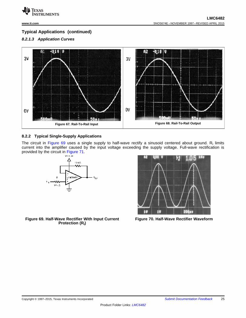
Typical Applications (continued)8.2.1.3 Application Curves
Figure 68. Rail-To-Rail OutputFigure 67. Rail-To-Rail Input
8.2.2 Typical Single-Supply ApplicationsThe circuit in Figure 69 uses a single supply to half-wave rectify a sinusoid centered about ground. RI limitscurrent into the amplifier caused by the input voltage exceeding the supply voltage. Full-wave rectification isprovided by the circuit in Figure 71.
Figure 69. Half-Wave Rectifier With Input Current Figure 70. Half-Wave Rectifier WaveformProtection (RI)
Copyright © 1997–2015, Texas Instruments Incorporated Submit Documentation Feedback 25
Product Folder Links: LMC6482

LMC6482SNOS674E –NOVEMBER 1997–REVISED APRIL 2015 www.ti.com
Typical Applications (continued)In Figure 75 dielectric absorption and leakage is minimized by using a polystyrene or polyethylene holdcapacitor. The droop rate is primarily determined by the value of CH and diode leakage current. The ultralowinput current of the LMC6482 has a negligible effect on droop.
Figure 71. Full-Wave Rectifier With Input Current Figure 72. Full-Wave Rectifier WaveformProtection (RI)
Figure 73. Large Compliance Range Current Figure 74. Positive Supply Current SenseSource
Figure 75. Low-Voltage Peak Detector With Rail-To-Rail Peak Capture Range
26 Submit Documentation Feedback Copyright © 1997–2015, Texas Instruments Incorporated
Product Folder Links: LMC6482

LMC6482www.ti.com SNOS674E –NOVEMBER 1997–REVISED APRIL 2015
Typical Applications (continued)The high CMRR (82 dB) of the LMC6482 allows excellent accuracy throughout the rail-to-rail dynamic capturerange of the circuit.
Figure 76. Rail-To-Rail Sample and Hold
The low-pass filter circuit in Figure 77 can be used as an anti-aliasing filter with the same voltage supply as theA/D converter.
Filter designs can also take advantage of the LMC6482 ultralow input current. The ultralow input current yieldsnegligible offset error even when large value resistors are used. This in turn allows the use of smaller valuedcapacitors which take less board space and cost less.
Figure 77. Rail-To-Rail Single Supply Low Pass Filter
Copyright © 1997–2015, Texas Instruments Incorporated Submit Documentation Feedback 27
Product Folder Links: LMC6482

LMC6482SNOS674E –NOVEMBER 1997–REVISED APRIL 2015 www.ti.com
9 Power Supply RecommendationsThe LMC6482 can be operated over a supply range of 3 V to 15 V. To achieve noise immunity as appropriate tothe application, it is important to use good PCB layout practices for power supply rails and planes, as well asusing bypass capacitors connected between the power supply pins and ground.
10 Layout
10.1 Layout GuidelinesIt is generally recognized that any circuit which must operate with less than 1000 pA of leakage current requiresspecial layout of the PC board. When one wishes to take advantage of the ultralow input current of theLMC6482, typically less than 20 fA, it is essential to have an excellent layout. Fortunately, the techniques ofobtaining low leakages are quite simple. First, the user must not ignore the surface leakage of the PCB, eventhrough it may sometimes appear acceptably low, because under conditions of high humidity or dust orcontamination, the surface leakage will be appreciable.
To minimize the effect of any surface leakage, lay out a ring of foil completely surrounding the LM6482s inputsand the terminals of capacitors, diodes, conductors, resistors, relay terminals, and so forth connected to theinputs of the op-amp, as in Figure 78. To have a significant effect, guard rings should be placed on both the topand bottom of the PCB. This PC foil must then be connected to a voltage which is at the same voltage as theamplifier inputs, because no leakage current can flow between two points at the same potential. For example, aPCB trace-to-pad resistance of 1012 Ω, which is normally considered a very large resistance, could leak 5 pA ifthe trace were a 5-V bus adjacent to the pad of the input. This would cause a 250 times degradation from theactual performance of the LMC6482. However, if a guard ring is held within 5 mV of the inputs, then even aresistance of 1011 Ω would cause only 0.05 pA of leakage current. See Figure 79 through Figure 81 for typicalconnections of guard rings for standard op-amp configurations.
The designer should be aware that when it is inappropriate to lay out a PCB for the sake of just a few circuits,another technique is even better than a guard ring on a PCB: Do not insert the input pin of the amplifier into thePCB at all, but bend it up in the air and use only air as an insulator. Air is an excellent insulator. In this case youmay have to forego some of the advantages of PCB construction, but the advantages are sometimes well worththe effort of using point-to-point up-in-the-air wiring. See Figure 82.
10.2 Layout Example
Figure 78. Example of Guard Ring in PCB Layout Typical Connections of Guard Rings
28 Submit Documentation Feedback Copyright © 1997–2015, Texas Instruments Incorporated
Product Folder Links: LMC6482

LMC6482www.ti.com SNOS674E –NOVEMBER 1997–REVISED APRIL 2015
Layout Example (continued)
Figure 79. Inverting Amplifier Typical Connections of Guard Rings
Figure 80. Noninverting Amplifier Typical Connections of Guard Rings
Figure 81. Follower Typical Connections of Guard Rings
(Input pins are lifted out of PCB and soldered directly to components. All other pins connected to PCB.)
Figure 82. Air Wiring
Copyright © 1997–2015, Texas Instruments Incorporated Submit Documentation Feedback 29
Product Folder Links: LMC6482

LMC6482SNOS674E –NOVEMBER 1997–REVISED APRIL 2015 www.ti.com
11 Device and Documentation Support
11.1 TrademarksAll trademarks are the property of their respective owners.
11.2 Electrostatic Discharge CautionThese devices have limited built-in ESD protection. The leads should be shorted together or the device placed in conductive foamduring storage or handling to prevent electrostatic damage to the MOS gates.
11.3 GlossarySLYZ022 — TI Glossary.
This glossary lists and explains terms, acronyms, and definitions.
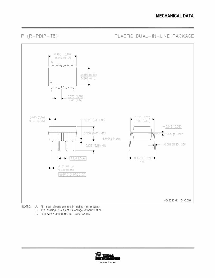
12 Mechanical, Packaging, and Orderable InformationThe following pages include mechanical, packaging, and orderable information. This information is the mostcurrent data available for the designated devices. This data is subject to change without notice and revision ofthis document. For browser-based versions of this data sheet, refer to the left-hand navigation.
30 Submit Documentation Feedback Copyright © 1997–2015, Texas Instruments Incorporated
Product Folder Links: LMC6482

PACKAGE OPTION ADDENDUM
www.ti.com 29-Jun-2017
Addendum-Page 1
PACKAGING INFORMATION
Orderable Device Status(1)
Package Type PackageDrawing
Pins PackageQty
Eco Plan(2)
Lead/Ball Finish(6)
MSL Peak Temp(3)
Op Temp (°C) Device Marking(4/5)
Samples
LMC6482AIM NRND SOIC D 8 95 TBD Call TI Call TI -40 to 85 LMC6482AIM
LMC6482AIM/NOPB ACTIVE SOIC D 8 95 Green (RoHS& no Sb/Br)
CU SN Level-1-260C-UNLIM -40 to 85 LMC6482AIM
LMC6482AIMX NRND SOIC D 8 2500 TBD Call TI Call TI -40 to 85 LMC6482AIM
LMC6482AIMX/NOPB ACTIVE SOIC D 8 2500 Green (RoHS& no Sb/Br)
CU SN Level-1-260C-UNLIM -40 to 85 LMC6482AIM
LMC6482AIN/NOPB ACTIVE PDIP P 8 40 Green (RoHS& no Sb/Br)
CU SN Level-1-NA-UNLIM -40 to 85 LMC6482AIN
LMC6482IM NRND SOIC D 8 95 TBD Call TI Call TI -40 to 85 LMC6482IM
LMC6482IM/NOPB ACTIVE SOIC D 8 95 Green (RoHS& no Sb/Br)
CU SN Level-1-260C-UNLIM -40 to 85 LMC6482IM
LMC6482IMM NRND VSSOP DGK 8 1000 TBD Call TI Call TI -40 to 85 A10
LMC6482IMM/NOPB ACTIVE VSSOP DGK 8 1000 Green (RoHS& no Sb/Br)
CU SN Level-1-260C-UNLIM -40 to 85 A10
LMC6482IMMX NRND VSSOP DGK 8 3500 TBD Call TI Call TI -40 to 85 A10
LMC6482IMMX/NOPB ACTIVE VSSOP DGK 8 3500 Green (RoHS& no Sb/Br)
CU SN Level-1-260C-UNLIM -40 to 85 A10
LMC6482IMX NRND SOIC D 8 2500 TBD Call TI Call TI -40 to 85 LMC6482IM
LMC6482IMX/NOPB ACTIVE SOIC D 8 2500 Green (RoHS& no Sb/Br)
CU SN Level-1-260C-UNLIM -40 to 85 LMC6482IM
LMC6482IN/NOPB ACTIVE PDIP P 8 40 Green (RoHS& no Sb/Br)
CU SN Level-1-NA-UNLIM -40 to 85 LMC6482IN
(1) The marketing status values are defined as follows:ACTIVE: Product device recommended for new designs.LIFEBUY: TI has announced that the device will be discontinued, and a lifetime-buy period is in effect.NRND: Not recommended for new designs. Device is in production to support existing customers, but TI does not recommend using this part in a new design.PREVIEW: Device has been announced but is not in production. Samples may or may not be available.OBSOLETE: TI has discontinued the production of the device.

PACKAGE OPTION ADDENDUM
www.ti.com 29-Jun-2017
Addendum-Page 2
(2) RoHS: TI defines "RoHS" to mean semiconductor products that are compliant with the current EU RoHS requirements for all 10 RoHS substances, including the requirement that RoHS substancedo not exceed 0.1% by weight in homogeneous materials. Where designed to be soldered at high temperatures, "RoHS" products are suitable for use in specified lead-free processes. TI mayreference these types of products as "Pb-Free".RoHS Exempt: TI defines "RoHS Exempt" to mean products that contain lead but are compliant with EU RoHS pursuant to a specific EU RoHS exemption.Green: TI defines "Green" to mean the content of Chlorine (Cl) and Bromine (Br) based flame retardants meet JS709B low halogen requirements of <=1000ppm threshold. Antimony trioxide basedflame retardants must also meet the <=1000ppm threshold requirement.
(3) MSL, Peak Temp. - The Moisture Sensitivity Level rating according to the JEDEC industry standard classifications, and peak solder temperature.
(4) There may be additional marking, which relates to the logo, the lot trace code information, or the environmental category on the device.
(5) Multiple Device Markings will be inside parentheses. Only one Device Marking contained in parentheses and separated by a "~" will appear on a device. If a line is indented then it is a continuationof the previous line and the two combined represent the entire Device Marking for that device.
(6) Lead/Ball Finish - Orderable Devices may have multiple material finish options. Finish options are separated by a vertical ruled line. Lead/Ball Finish values may wrap to two lines if the finishvalue exceeds the maximum column width.
Important Information and Disclaimer:The information provided on this page represents TI's knowledge and belief as of the date that it is provided. TI bases its knowledge and belief on informationprovided by third parties, and makes no representation or warranty as to the accuracy of such information. Efforts are underway to better integrate information from third parties. TI has taken andcontinues to take reasonable steps to provide representative and accurate information but may not have conducted destructive testing or chemical analysis on incoming materials and chemicals.TI and TI suppliers consider certain information to be proprietary, and thus CAS numbers and other limited information may not be available for release.
In no event shall TI's liability arising out of such information exceed the total purchase price of the TI part(s) at issue in this document sold by TI to Customer on an annual basis.
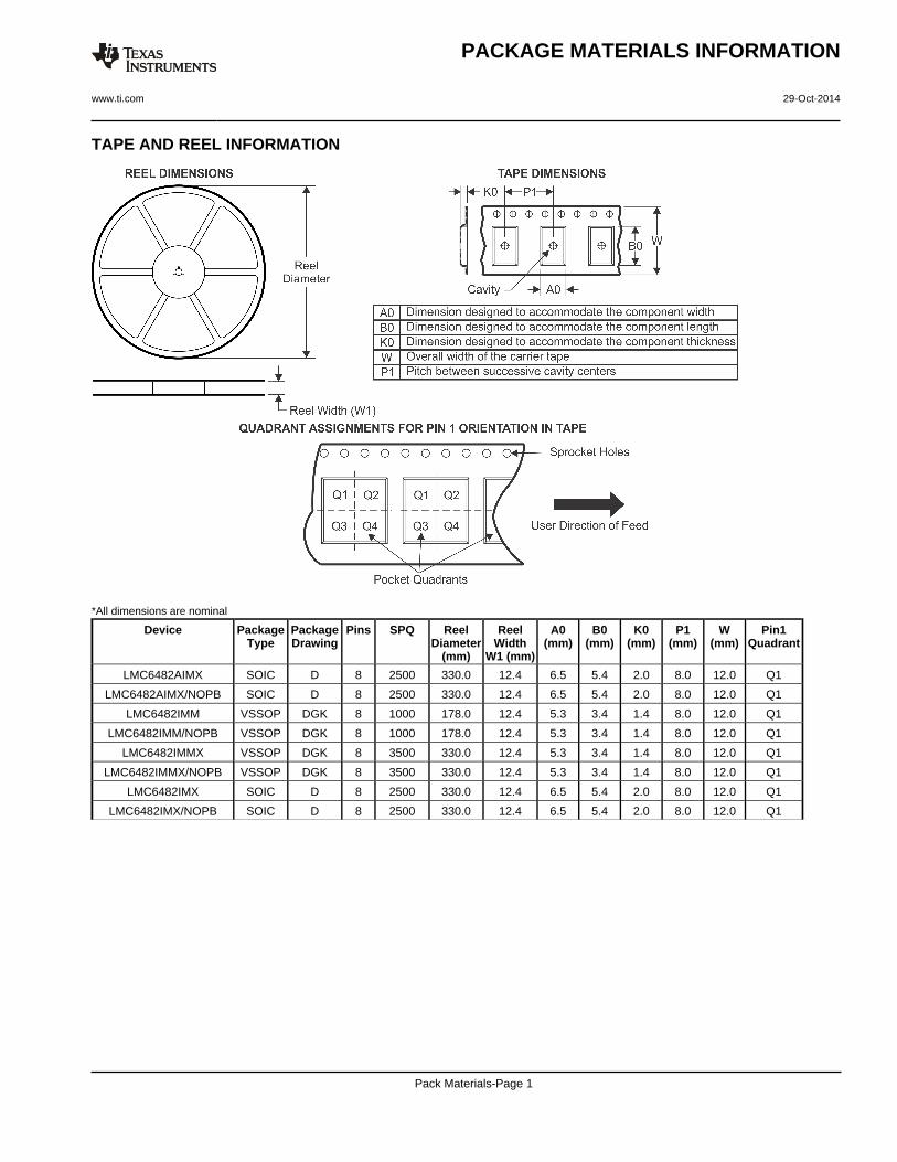
TAPE AND REEL INFORMATION
*All dimensions are nominal
Device PackageType
PackageDrawing
Pins SPQ ReelDiameter
(mm)
ReelWidth
W1 (mm)
A0(mm)
B0(mm)
K0(mm)
P1(mm)
W(mm)
Pin1Quadrant
LMC6482AIMX SOIC D 8 2500 330.0 12.4 6.5 5.4 2.0 8.0 12.0 Q1
LMC6482AIMX/NOPB SOIC D 8 2500 330.0 12.4 6.5 5.4 2.0 8.0 12.0 Q1
LMC6482IMM VSSOP DGK 8 1000 178.0 12.4 5.3 3.4 1.4 8.0 12.0 Q1
LMC6482IMM/NOPB VSSOP DGK 8 1000 178.0 12.4 5.3 3.4 1.4 8.0 12.0 Q1
LMC6482IMMX VSSOP DGK 8 3500 330.0 12.4 5.3 3.4 1.4 8.0 12.0 Q1
LMC6482IMMX/NOPB VSSOP DGK 8 3500 330.0 12.4 5.3 3.4 1.4 8.0 12.0 Q1
LMC6482IMX SOIC D 8 2500 330.0 12.4 6.5 5.4 2.0 8.0 12.0 Q1
LMC6482IMX/NOPB SOIC D 8 2500 330.0 12.4 6.5 5.4 2.0 8.0 12.0 Q1
PACKAGE MATERIALS INFORMATION
www.ti.com 29-Oct-2014
Pack Materials-Page 1

*All dimensions are nominal
Device Package Type Package Drawing Pins SPQ Length (mm) Width (mm) Height (mm)
LMC6482AIMX SOIC D 8 2500 367.0 367.0 35.0
LMC6482AIMX/NOPB SOIC D 8 2500 367.0 367.0 35.0
LMC6482IMM VSSOP DGK 8 1000 210.0 185.0 35.0
LMC6482IMM/NOPB VSSOP DGK 8 1000 210.0 185.0 35.0
LMC6482IMMX VSSOP DGK 8 3500 367.0 367.0 35.0
LMC6482IMMX/NOPB VSSOP DGK 8 3500 367.0 367.0 35.0
LMC6482IMX SOIC D 8 2500 367.0 367.0 35.0
LMC6482IMX/NOPB SOIC D 8 2500 367.0 367.0 35.0
PACKAGE MATERIALS INFORMATION
www.ti.com 29-Oct-2014
Pack Materials-Page 2


IMPORTANT NOTICE
Texas Instruments Incorporated (TI) reserves the right to make corrections, enhancements, improvements and other changes to itssemiconductor products and services per JESD46, latest issue, and to discontinue any product or service per JESD48, latest issue. Buyersshould obtain the latest relevant information before placing orders and should verify that such information is current and complete.TI’s published terms of sale for semiconductor products (http://www.ti.com/sc/docs/stdterms.htm) apply to the sale of packaged integratedcircuit products that TI has qualified and released to market. Additional terms may apply to the use or sale of other types of TI products andservices.Reproduction of significant portions of TI information in TI data sheets is permissible only if reproduction is without alteration and isaccompanied by all associated warranties, conditions, limitations, and notices. TI is not responsible or liable for such reproduceddocumentation. Information of third parties may be subject to additional restrictions. Resale of TI products or services with statementsdifferent from or beyond the parameters stated by TI for that product or service voids all express and any implied warranties for theassociated TI product or service and is an unfair and deceptive business practice. TI is not responsible or liable for any such statements.Buyers and others who are developing systems that incorporate TI products (collectively, “Designers”) understand and agree that Designersremain responsible for using their independent analysis, evaluation and judgment in designing their applications and that Designers havefull and exclusive responsibility to assure the safety of Designers' applications and compliance of their applications (and of all TI productsused in or for Designers’ applications) with all applicable regulations, laws and other applicable requirements. Designer represents that, withrespect to their applications, Designer has all the necessary expertise to create and implement safeguards that (1) anticipate dangerousconsequences of failures, (2) monitor failures and their consequences, and (3) lessen the likelihood of failures that might cause harm andtake appropriate actions. Designer agrees that prior to using or distributing any applications that include TI products, Designer willthoroughly test such applications and the functionality of such TI products as used in such applications.TI’s provision of technical, application or other design advice, quality characterization, reliability data or other services or information,including, but not limited to, reference designs and materials relating to evaluation modules, (collectively, “TI Resources”) are intended toassist designers who are developing applications that incorporate TI products; by downloading, accessing or using TI Resources in anyway, Designer (individually or, if Designer is acting on behalf of a company, Designer’s company) agrees to use any particular TI Resourcesolely for this purpose and subject to the terms of this Notice.TI’s provision of TI Resources does not expand or otherwise alter TI’s applicable published warranties or warranty disclaimers for TIproducts, and no additional obligations or liabilities arise from TI providing such TI Resources. TI reserves the right to make corrections,enhancements, improvements and other changes to its TI Resources. TI has not conducted any testing other than that specificallydescribed in the published documentation for a particular TI Resource.Designer is authorized to use, copy and modify any individual TI Resource only in connection with the development of applications thatinclude the TI product(s) identified in such TI Resource. NO OTHER LICENSE, EXPRESS OR IMPLIED, BY ESTOPPEL OR OTHERWISETO ANY OTHER TI INTELLECTUAL PROPERTY RIGHT, AND NO LICENSE TO ANY TECHNOLOGY OR INTELLECTUAL PROPERTYRIGHT OF TI OR ANY THIRD PARTY IS GRANTED HEREIN, including but not limited to any patent right, copyright, mask work right, orother intellectual property right relating to any combination, machine, or process in which TI products or services are used. Informationregarding or referencing third-party products or services does not constitute a license to use such products or services, or a warranty orendorsement thereof. Use of TI Resources may require a license from a third party under the patents or other intellectual property of thethird party, or a license from TI under the patents or other intellectual property of TI.TI RESOURCES ARE PROVIDED “AS IS” AND WITH ALL FAULTS. TI DISCLAIMS ALL OTHER WARRANTIES ORREPRESENTATIONS, EXPRESS OR IMPLIED, REGARDING RESOURCES OR USE THEREOF, INCLUDING BUT NOT LIMITED TOACCURACY OR COMPLETENESS, TITLE, ANY EPIDEMIC FAILURE WARRANTY AND ANY IMPLIED WARRANTIES OFMERCHANTABILITY, FITNESS FOR A PARTICULAR PURPOSE, AND NON-INFRINGEMENT OF ANY THIRD PARTY INTELLECTUALPROPERTY RIGHTS. TI SHALL NOT BE LIABLE FOR AND SHALL NOT DEFEND OR INDEMNIFY DESIGNER AGAINST ANY CLAIM,INCLUDING BUT NOT LIMITED TO ANY INFRINGEMENT CLAIM THAT RELATES TO OR IS BASED ON ANY COMBINATION OFPRODUCTS EVEN IF DESCRIBED IN TI RESOURCES OR OTHERWISE. IN NO EVENT SHALL TI BE LIABLE FOR ANY ACTUAL,DIRECT, SPECIAL, COLLATERAL, INDIRECT, PUNITIVE, INCIDENTAL, CONSEQUENTIAL OR EXEMPLARY DAMAGES INCONNECTION WITH OR ARISING OUT OF TI RESOURCES OR USE THEREOF, AND REGARDLESS OF WHETHER TI HAS BEENADVISED OF THE POSSIBILITY OF SUCH DAMAGES.Unless TI has explicitly designated an individual product as meeting the requirements of a particular industry standard (e.g., ISO/TS 16949and ISO 26262), TI is not responsible for any failure to meet such industry standard requirements.Where TI specifically promotes products as facilitating functional safety or as compliant with industry functional safety standards, suchproducts are intended to help enable customers to design and create their own applications that meet applicable functional safety standardsand requirements. Using products in an application does not by itself establish any safety features in the application. Designers mustensure compliance with safety-related requirements and standards applicable to their applications. Designer may not use any TI products inlife-critical medical equipment unless authorized officers of the parties have executed a special contract specifically governing such use.Life-critical medical equipment is medical equipment where failure of such equipment would cause serious bodily injury or death (e.g., lifesupport, pacemakers, defibrillators, heart pumps, neurostimulators, and implantables). Such equipment includes, without limitation, allmedical devices identified by the U.S. Food and Drug Administration as Class III devices and equivalent classifications outside the U.S.TI may expressly designate certain products as completing a particular qualification (e.g., Q100, Military Grade, or Enhanced Product).Designers agree that it has the necessary expertise to select the product with the appropriate qualification designation for their applicationsand that proper product selection is at Designers’ own risk. Designers are solely responsible for compliance with all legal and regulatoryrequirements in connection with such selection.Designer will fully indemnify TI and its representatives against any damages, costs, losses, and/or liabilities arising out of Designer’s non-compliance with the terms and provisions of this Notice.
Mailing Address: Texas Instruments, Post Office Box 655303, Dallas, Texas 75265Copyright © 2017, Texas Instruments Incorporated