Embed Size (px)
Citation preview
LTC4380
1Rev. C
For more information www.analog.com
TYPICAL APPLICATION
FEATURES DESCRIPTION
Low Quiescent Current Surge Stopper
The LTC®4380 low quiescent current surge stopper protects loads from high voltage transients. Overvoltage protection is provided by clamping the gate voltage of an external N-channel MOSFET to limit the output voltage to a safe value during overvoltage events such as load dump in automobiles. Fixed gate clamp voltages are selectable for 12V and 24V/28V systems. For systems of any voltage up to 72V, use the adjustable gate clamp versions. Overcur-rent protection is also provided.
An internal multiplier generates a TMR pin current pro-portional to VDS and ID, so that operating time in both overcurrent and overvoltage conditions is limited in ac-cordance with MOSFET stress.
The GATE pin can drive back-to-back MOSFETs for reverse input protection, eliminating the voltage drop and dissi-pation of a Schottky diode solution. A low 8µA operating current permits use in always-on and battery powered applications. An accurate ON pin comparator monitors the input supply for undervoltage (UV) conditions and also serves as a shutdown input, reducing the quiescent current to 6µA.
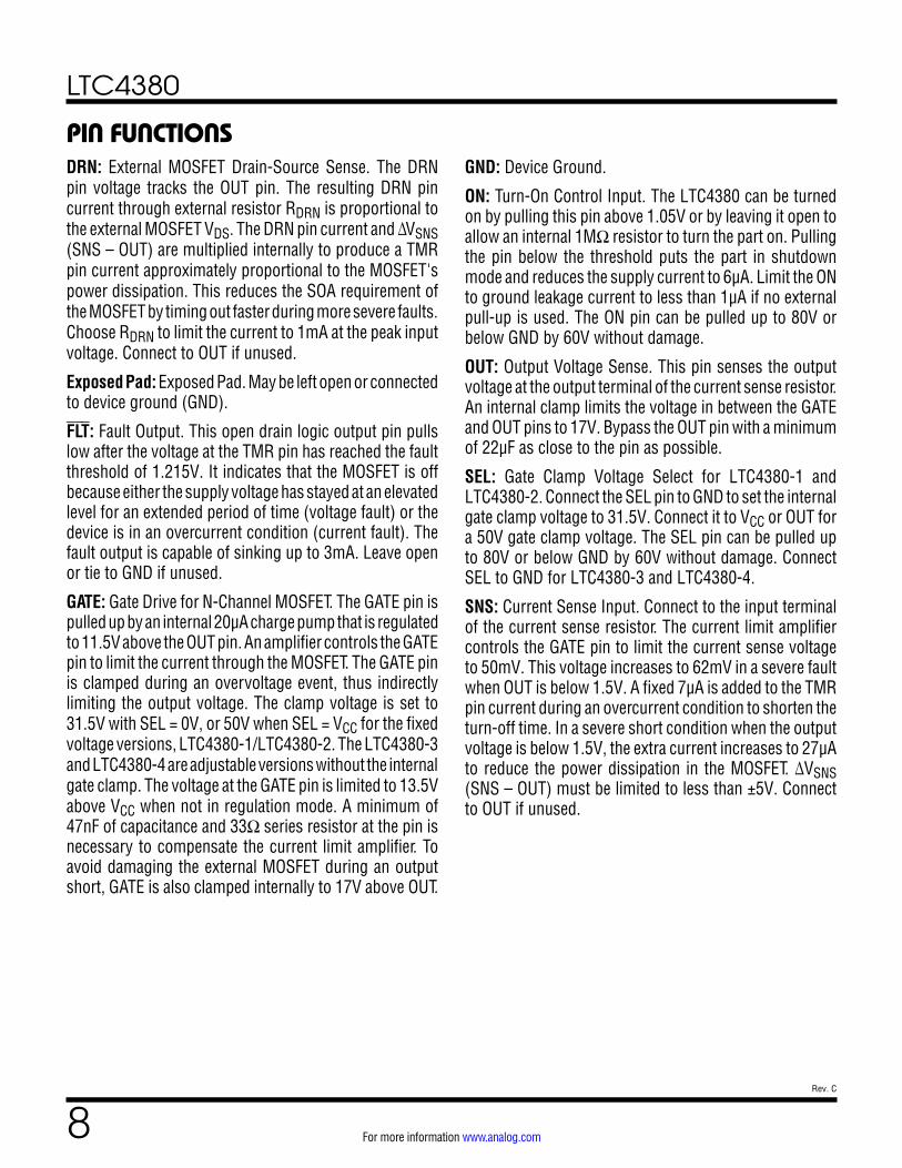
12V, 1A with 250V Overvoltage Protection Surge Stopper Limits Output to 27V During Input Surge
APPLICATIONS
n Low Quiescent Current: 8µA Operating n Withstands Surge Voltage Up to the MOSFET Limit n Wide Operating Voltage Range: 4V to 72V n Overcurrent Protection n Selectable Internal 31.5V/50V or Adjustable Gate
Clamp Voltage n Reverse Input Protection to –60V n Adjustable Turn-On Threshold n Adjustable Fault Timer with MOSFET Stress
Acceleration n Controls N-Channel MOSFET n Latchoff and Retry Options n Low Retry Duty Cycle During Faults n 10-Pin DFN (3mm × 3mm) and MSOP Packages n AEC-Q100 Qualified for Automotive Applications
n Automotive/Avionic/Industrial Surge Protection n Hot Swap, Live Insertion n High Side Switch for Battery Powered Systems n Automotive Load Dump Protection
All registered trademarks and trademarks are the property of their respective owners. Protected by U.S. patents, including 9634481.
FDB33N25
68VCMHZ5266B
0.1µF
10Ω33Ω
10k
12V/1AOUTPUT CLAMPED AT 27V
VIN12V
(250VPK)
47nF
249k
20mΩ
GATEDRN SNS OUT
VCC
ONFLT
SELTMR
LTC4380-2
GND
4380 TA01a
8.2µF
22µF
VIN20V/DIV
VOUT20V/DIV
100ms/DIV 4380 TA01b
100V INPUT SURGE
12V
12V
27V ADJUSTABLE CLAMP
CTMR = 8.2µFILOAD = 1A
Document Feedback
LTC4380
2Rev. C
For more information www.analog.com
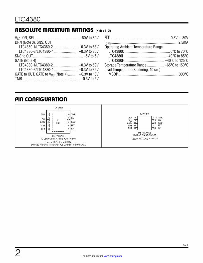
ABSOLUTE MAXIMUM RATINGSVCC, ON, SEL ............................................... –60V to 80VDRN (Note 3), SNS, OUT
LTC4380-1/LTC4380-2........................... –0.3V to 53V LTC4380-3/LTC4380-4 .......................... –0.3V to 80V
SNS to OUT ..................................................... –5V to 5VGATE (Note 4)
LTC4380-1/LTC4380-2........................... –0.3V to 53V LTC4380-3/LTC4380-4 .......................... –0.3V to 86V
GATE to OUT, GATE to VCC (Note 4) ........... –0.3V to 10VTMR ............................................................. –0.3V to 5V
(Notes 1, 2)
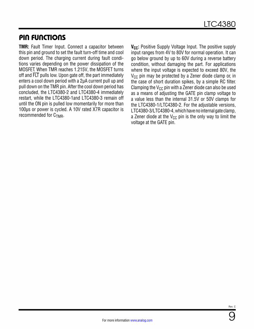
TOP VIEW
DD PACKAGE10-LEAD (3mm × 3mm) PLASTIC DFN
10
11GND
9
6
7
8
4
5
3
2
1 TMR
ON
GND
FLT
SEL
DRN
VCC
GATE
SNS
OUT
TJMAX = 135°C, θJA = 43°C/W
EXPOSED PAD (PIN 11) IS GND, PCB CONNECTION OPTIONAL
12345
DRNVCC
GATESNSOUT
109876
TMRONGNDFLTSEL
TOP VIEW
MS PACKAGE10-LEAD PLASTIC MSOP
TJMAX = 150°C, θJA = 160°C/W
PIN CONFIGURATION
FLT ............................................................. –0.3V to 80VIDRN .......................................................................2.5mAOperating Ambient Temperature Range
LTC4380C ................................................ 0°C to 70°C LTC4380I .............................................–40°C to 85°C LTC4380H .......................................... –40°C to 125°C
Storage Temperature Range .................. –65°C to 150°CLead Temperature (Soldering, 10 sec)
MSOP ............................................................... 300°C

LTC4380
3Rev. C
For more information www.analog.com
ORDER INFORMATIONLEAD FREE FINISH TAPE AND REEL PART MARKING* PACKAGE DESCRIPTION TEMPERATURE RANGELTC4380CDD-1#PBF LTC4380CDD-1#TRPBF LGHQ 10-Lead (3mm × 3mm) Plastic DFN 0°C to 70°C
LTC4380IDD-1#PBF LTC4380IDD-1#TRPBF LGHQ 10-Lead (3mm × 3mm) Plastic DFN –40°C to 85°C
LTC4380HDD-1#PBF LTC4380HDD-1#TRPBF LGHQ 10-Lead (3mm × 3mm) Plastic DFN –40°C to 125°C
LTC4380CMS-1#PBF LTC4380CMS-1#TRPBF LTGHR 10-Lead Plastic MSOP 0°C to 70°C
LTC4380IMS-1#PBF LTC4380IMS-1#TRPBF LTGHR 10-Lead Plastic MSOP –40°C to 85°C
LTC4380HMS-1#PBF LTC4380HMS-1#TRPBF LTGHR 10-Lead Plastic MSOP –40°C to 125°C
LTC4380CDD-2#PBF LTC4380CDD-2#TRPBF LGHS 10-Lead (3mm × 3mm) Plastic DFN 0°C to 70°C
LTC4380IDD-2#PBF LTC4380IDD-2#TRPBF LGHS 10-Lead (3mm × 3mm) Plastic DFN –40°C to 85°C
LTC4380HDD-2#PBF LTC4380HDD-2#TRPBF LGHS 10-Lead (3mm × 3mm) Plastic DFN –40°C to 125°C
LTC4380CMS-2#PBF LTC4380CMS-2#TRPBF LTGHT 10-Lead Plastic MSOP 0°C to 70°C
LTC4380IMS-2#PBF LTC4380IMS-2#TRPBF LTGHT 10-Lead Plastic MSOP –40°C to 85°C
LTC4380HMS-2#PBF LTC4380HMS-2#TRPBF LTGHT 10-Lead Plastic MSOP –40°C to 125°C
LTC4380CDD-3#PBF LTC4380CDD-3#TRPBF LGXZ 10-Lead (3mm × 3mm) Plastic DFN 0°C to 70°C
LTC4380IDD-3#PBF LTC4380IDD-3#TRPBF LGXZ 10-Lead (3mm × 3mm) Plastic DFN –40°C to 85°C
LTC4380HDD-3#PBF LTC4380HDD-3#TRPBF LGXZ 10-Lead (3mm × 3mm) Plastic DFN –40°C to 125°C
LTC4380CMS-3#PBF LTC4380CMS-3#TRPBF LTGYD 10-Lead Plastic MSOP 0°C to 70°C
LTC4380IMS-3#PBF LTC4380IMS-3#TRPBF LTGYD 10-Lead Plastic MSOP –40°C to 85°C
LTC4380HMS-3#PBF LTC4380HMS-3#TRPBF LTGYD 10-Lead Plastic MSOP –40°C to 125°C
LTC4380CDD-4#PBF LTC4380CDD-4#TRPBF LGYC 10-Lead (3mm × 3mm) Plastic DFN 0°C to 70°C
LTC4380IDD-4#PBF LTC4380IDD-4#TRPBF LGYC 10-Lead (3mm × 3mm) Plastic DFN –40°C to 85°C
LTC4380HDD-4#PBF LTC4380HDD-4#TRPBF LGYC 10-Lead (3mm × 3mm) Plastic DFN –40°C to 125°C
LTC4380CMS-4#PBF LTC4380CMS-4#TRPBF LTGYF 10-Lead Plastic MSOP 0°C to 70°C
LTC4380IMS-4#PBF LTC4380IMS-4#TRPBF LTGYF 10-Lead Plastic MSOP –40°C to 85°C
LTC4380HMS-4#PBF LTC4380HMS-4#TRPBF LTGYF 10-Lead Plastic MSOP –40°C to 125°C
AUTOMOTIVE PRODUCTS**LTC4380IMS-1#WPBF LTC4380IMS-1#WTRPBF LTGHR 10-Lead Plastic MSOP –40°C to 85°C
LTC4380HMS-1#WPBF LTC4380HMS-1#WTRPBF LTGHR 10-Lead Plastic MSOP –40°C to 125°C
LTC4380IMS-2#WPBF LTC4380IMS-2#WTRPBF LTGHT 10-Lead Plastic MSOP –40°C to 85°C
LTC4380HMS-2#WPBF LTC4380HMS-2#WTRPBF LTGHT 10-Lead Plastic MSOP –40°C to 125°C
LTC4380IMS-3#WPBF LTC4380IMS-3#WTRPBF LTGYD 10-Lead Plastic MSOP –40°C to 85°C
LTC4380HMS-3#WPBF LTC4380HMS-3#WTRPBF LTGYD 10-Lead Plastic MSOP –40°C to 125°C
LTC4380IMS-4#WPBF LTC4380IMS-4#WTRPBF LTGYF 10-Lead Plastic MSOP –40°C to 85°C
LTC4380HMS-4#WPBF LTC4380HMS-4#WTRPBF LTGYF 10-Lead Plastic MSOP –40°C to 125°C
Contact the factory for parts specified with wider operating temperature ranges. *The temperature grade is identified by a label on the shipping container.
Tape and reel specifications. Some packages are available in 500 unit reels through designated sales channels with #TRMPBF suffix.**Versions of this part are available with controlled manufacturing to support the quality and reliability requirements of automotive applications. These
models are designated with a #W suffix. Only the automotive grade products shown are available for use in automotive applications. Contact your local Analog Devices account representative for specific product ordering information and to obtain the specific Automotive Reliability reports for these models.
LTC4380
4Rev. C
For more information www.analog.com
ELECTRICAL CHARACTERISTICS The l denotes the specifications which apply over the full operating temperature range, otherwise specifications are at TA = 25°C. VCC = OUT = SNS = DRN = 12V, unless otherwise noted.
SYMBOL PARAMETER CONDITIONS MIN TYP MAX UNITS
Supply
VCC Operating Voltage Range LTC4380-1/LTC4380-2 LTC4380-3/LTC4380-4 (Note 6)
l
l
4 4
80 72
V V
VOUT Operating Voltage Range l 72 V
IQ Total Supply Current (Note 5)
C-Grade and I-Grade H-Grade
l
l
8 11 12 20
µA µA µA
VCC = OUT = SNS = DRN = 4V
l
22 28 35
µA µA
ICC VCC Current, Shutdown ON = OUT = SNS = 0V l 6 10 µA
VCC Current
l
7 9 12
µA µA
VCC = OUT = SNS = DRN = 4V
l
20 25 30
µA µA
ISNS SNS Current l 0.5 1.4 µA
IOUT OUT Current OUT Current, Shutdown
C-Grade and I-Grade H-Grade
l
l
l
1.5 5
5.5 12 80
µA µA µA
IR Reverse Input Current VCC = –60V, ON Open, SEL = 0V VCC = ON = SEL = –60V
l
l
–0.4 –1.2
–2 –5
mA mA
Gate Drive
∆VGATE GATE Drive (GATE – OUT) SEL = SNS = OUT = VCC =12V 8V ≤ VCC ≤ 30V; IGATE = –1µA, 0µA VCC = 4V; IGATE = –1µA, 0µA
l
l
10 5
11.5
14 8
V V
∆VCLAMP GATE Clamp to VCC (GATE – VCC) SNS = OUT = 20V, IGATE = 0µA l 12 13.5 14.5 V
VGATE GATE Clamp to GND VCC = 30V, SEL = 0V (LTC4380-1/LTC4380-2) VCC = 60V, SEL = VCC (LTC4380-1/LTC4380-2)
l
l
30 47.5
31.5 50
33 52.5
V V
IGATE(UP) GATE Pull-Up Current VCC = GATE = OUT = 12V, SEL = 0V VCC = GATE = OUT = 24V, SEL = VCC
l
l
–10 –12
–20 –25
–30 –35
µA µA
IGATE(DN) GATE Pull-Down Current Overcurrent Shutdown Input UV Fault Time Out
∆VSNS = 200mV, GATE = 12V, OUT = 0V ON = 0V, GATE = 20V VCC = 3.5V, GATE = 10V TMR = 2V, GATE = 10V
l
l
l
l
50 0.3 2
1.5
100 5 5
3.5
mA mA mA mA
Current Limit∆VSNS Current Limit Sense Voltage (SNS – OUT) VCC = 12V, 24V, OUT = 6V, 12V
VCC = 12V, 24V, OUT = 0Vl
l
45 42
50 62
55 95
mV mV
tOFF(OC) Overcurrent Turn-Off Propagation Delay ∆VSNS Steps from 0V to 250mV, OUT = 6V l 2 4 µs
∆VSNS Steps from 0V to 250mV, OUT = 0V l 2 4 µs
SEL, FLTISEL SEL Input Current SEL = 0V to 80V l ±0.1 µA
VSEL SEL Input Threshold l 0.4 3 V
IFLT FLT Leakage Current FLT = 80V l 2 µA
VFLT(LOW) FLT Output Low ISINK = 0.1mA ISINK = 3mA
l
l
0.1 1
0.5 4
V V
LTC4380
5Rev. C
For more information www.analog.com
The l denotes the specifications which apply over the full operating temperature range, otherwise specifications are at TA = 25°C. VCC = OUT = SNS = DRN = 12V, unless otherwise noted.SYMBOL PARAMETER CONDITIONS MIN TYP MAX UNITS
TMR, DRN∆VDRN DRN Voltage (DRN – OUT) IDRN = 0.1mA, OUT = SNS = 12V l 0.7 1.5 2.5 V
VDS(MAX) Overvoltage VDS Threshold (DRN – OUT) TMR = 0.8V, IDRN = 2µA SNS = OUT = 12V
l
0.6 0.3
0.7 0.8 1.0
V V
ITMR(DN) TMR Pull-Down Current TMR = 0.8V l 1.25 2 2.75 µA
ITMR(UP,COOL) TMR Pull-Up Current, Cool Down TMR = 2V l –1 –2 –3 µA
ITMR(UP) TMR Pull-Up Current, Overvoltage
Small OV, Light Load High OV, Light Load
Small OV, Heavy Load High OV, Heavy Load
TMR = 0.8V, OUT = 11V, IDRN = 5µA, ∆VSNS = 0mV l –0.8 –1.6 –2.4 µA
OUT = 28V, TMR = 0.8V IDRN = 0.1mA, ∆VSNS = 10mV IDRN = 1mA, ∆VSNS = 10mV
l
l
–3.5 –13
–6.7 –30
–11.6 –61
µA µA
IDRN = 0.1mA, ∆VSNS = 40mV IDRN = 1mA, ∆VSNS = 40mV
l
l
–10 –60
–20 –120
–30 –180
µA µA
TMR Pull-Up Current, Overcurrent
Small OV, Light Load High OV, Light Load
Small OV, Heavy Load High OV, Heavy Load
TMR = 0.8V IDRN = 0mA, OUT = 11V IDRN = 0mA, OUT = 0V
l
l
–4
–17
–6
–27
–9
–34
µA µA
IDRN = 0.1mA, OUT = 11V IDRN = 1mA, OUT = 11V
l
l
–16 –80
–27 –142
–38 –200
µA µA
IDRN = 0.1mA, OUT = 0V IDRN = 1mA, OUT = 0V
l
l
–35 –130
–50 –170
–60 –220
µA µA
VTMR(F) TMR Gate Off Threshold TMR Rising l 1.178 1.215 1.251 V
D Retry Duty Cycle; Overvoltage, LTC4380-2/LTC4380-4
∆VSNS = 40mV, IDRN = 5µA, OUT = 28V, VCC = 29V l 2.8 3.5 %
∆VSNS = 40mV, IDRN = 500µA, OUT = 28V, VCC = 80V
l 0.1 0.2 %
Retry Duty Cycle; Overcurrent, LTC4380-2/LTC4380-4
IDRN = 500µA OUT = 0V, VCC = 14V OUT = 6V, VCC = 14V
l
l
0.1
0.35
0.2 0.7
% %
ONION ON Input Current VON = 1V l –1 –2 µA
VON ON Input Threshold ON Rising l 0.99 1.05 1.1 V
VON(HYST) ON Input Hysteresis 45 mV
tON(ON) Turn-On Propagation Delay ON Steps from 0V to 1.5V, OUT = SNS = 0V l 5 25 ms
tOFF(ON) Turn-Off Propagation Delay ON Steps from 1.5V to 0V, OUT = SNS = VCC l 1 5 µs
ELECTRICAL CHARACTERISTICS
Note 1: Stresses beyond those listed under Absolute Maximum Ratings may cause permanent damage to the device. Exposure to any Absolute Maximum Rating condition for extended periods may affect device reliability and lifetime.Note 2: All currents into device pins are positive; all currents out of device pins are negative. All voltages are referenced to GND unless otherwise specified.Note 3: Internal clamps limit the DRN pin to a minimum of 10V above the OUT and SNS pins.
Note 4: Internal clamps limit the GATE pin to a minimum of 10V above the OUT pin or VCC pin, or 50V (SEL = VCC) or 31.5V (SEL = GND) above the GND pin (LTC4380-1/LTC4380-2). Driving this pin to voltages beyond the clamp may damage the device.Note 5: Total supply current is the sum of the current into the VCC, OUT, SNS and DRN pins.Note 6: Operating voltage is limited by the maximum GATE voltage of 86V.
LTC4380
6Rev. C
For more information www.analog.com
TYPICAL PERFORMANCE CHARACTERISTICS
Supply Current (ICC) vs Supply Voltage
Supply Current (ICC) vs Temperature ISNS vs Temperature
Output Pin Current vs Temperature
Reverse Current vs Reverse Voltage
Total Supply Current (IQ) vs Input Voltage
Total Supply Current (IQ) vs Gate Leakage
Total Supply Current (IQ) vs Temperature
VCC = 12V, unless otherwise noted.
SEL = VCC
IGATE = 0SHUTDOWN
VIN (V)0 10 20 30
0
10
20
30
I Q (µ
A)
4380 G01
SNS = OUT= SEL = VCC
VCC (V)0 10 20 30
0
10
20
30
I CC
(µA)
4380 G04
SNS = OUT = VCC
ONSHUTDOWN
TEMPERATURE (°C)–50 –25 0 25 50 75 100 125 150
1
10
100
1k
I OUT
(µA)
4380 G07
IGATE (µA)–0.001 –0.01 –0.1 –1 –101
10
100
I Q (µ
A)
4380 G02
SNS = OUT = VCC
VCC = 4VVCC = 12V
TEMPERATURE (°C)–50 –25 0 25 50 75 100 125 150
1
10
100
I CC
(µA)
4380 G05
SEL = ON = VCC
VCC (V)–10 –20 –30 –40 –50 –60 –70 –80
0.1
1
10
I GND
(mA)
4380 G08
SNS = OUT = VCC
TEMPERATURE (°C)–50 –25 0 25 50 75 100 125 150
0.1
1
10
I SNS
(µA)
4380 G06
GATE = 0VGATE = 12V
TEMPERATURE (°C)–50 –25 0 25 50 75 100 125 150
–15
–20
–25
–30
–35
I GAT
E(UP
) (µA
)
4380 G09
IGATE = 0IGATE = –1µASHUTDOWN
TEMPERATURE (°C)–50 –25 0 25 50 75 100 125 150
1
10
100
I Q (µ
A)
4380 G03
Gate Pull Up Current vs Temperature
LTC4380
7Rev. C
For more information www.analog.com
Gate Drive vs Gate Current
TYPICAL PERFORMANCE CHARACTERISTICS
ON Pin Current vs Voltage
Gate Clamp to VCC vs Temperature
TMR Pin Current vs Temperature, Overcurrent Fault
TMR Pin Current vs Temperature, Overvoltage Fault
Current Limit vs Output Voltage DRN Voltage vs Current
Gate Drive vs Temperature Gate Drive vs Supply Voltage
VCC = 12V, unless otherwise noted.
VCC = 12VVCC = 4V
IGATE (µA)0 –5 –10 –15 –20 –25
0
2
4
6
8
10
12
14
∆VGA
TE (V
)
4380 G10
OUT = 20V
TEMPERATURE (°C)–50 –25 0 25 50 75 100 125 150
11
12
13
14
15
∆VCL
AMP
(V)
4380 G13
VOUT (V)0 1 2 3 4 5 6 7 8
0
10
20
30
40
50
60
70
∆VSN
S (m
V)
4380 G16
IGATE = –1µA
VCC = 4VVCC = 12V
TEMPERATURE (°C)–50 –25 0 25 50 75 100 125 150
0
5
10
15
∆VGA
TE (V
)
4380 G11
IDRN = 0.1mA
OUT = 0VOUT = 6V
TEMPERATURE (°C)–50 –25 0 25 50 75 100 125 150
–20
–25
–30
–35
–40
–45
–50
–55
–60
I TM
R(OC
) (µA
)
4380 G14
∆VDRN = VDRN – VOUT
IDRN (µA)1 10 100 1k
1.0
1.5
2.0
2.5
3.0
3.5
4.0
∆VDR
N (V
)
4380 G17
IGATE = –1µA
SEL = VCC
VCC (V)0 10 20 30
0
5
10
15
∆VGA
TE (V
)
4380 G12
IDRN = 1mA
∆VSNS = 40mV∆VSNS = 10mV
TEMPERATURE (°C)–50 –25 0 25 50 75 100 125 150
–20
–40
–60
–80
–100
–120
–140
–160
I TM
R(OV
) (µA
)
4380 G15
VON (V)0 1 2 3 4 5
0
–0.5
–1.0
–1.5
–2.0
–2.5
–3.0
–3.5
–4.0
I ON
(µA)
4380 G18
LTC4380
8Rev. C
For more information www.analog.com
PIN FUNCTIONSDRN: External MOSFET Drain-Source Sense. The DRN pin voltage tracks the OUT pin. The resulting DRN pin current through external resistor RDRN is proportional to the external MOSFET VDS. The DRN pin current and ∆VSNS (SNS – OUT) are multiplied internally to produce a TMR pin current approximately proportional to the MOSFET's power dissipation. This reduces the SOA requirement of the MOSFET by timing out faster during more severe faults. Choose RDRN to limit the current to 1mA at the peak input voltage. Connect to OUT if unused.
Exposed Pad: Exposed Pad. May be left open or connected to device ground (GND).
FLT: Fault Output. This open drain logic output pin pulls low after the voltage at the TMR pin has reached the fault threshold of 1.215V. It indicates that the MOSFET is off because either the supply voltage has stayed at an elevated level for an extended period of time (voltage fault) or the device is in an overcurrent condition (current fault). The fault output is capable of sinking up to 3mA. Leave open or tie to GND if unused.
GATE: Gate Drive for N-Channel MOSFET. The GATE pin is pulled up by an internal 20µA charge pump that is regulated to 11.5V above the OUT pin. An amplifier controls the GATE pin to limit the current through the MOSFET. The GATE pin is clamped during an overvoltage event, thus indirectly limiting the output voltage. The clamp voltage is set to 31.5V with SEL = 0V, or 50V when SEL = VCC for the fixed voltage versions, LTC4380-1/LTC4380-2. The LTC4380-3 and LTC4380-4 are adjustable versions without the internal gate clamp. The voltage at the GATE pin is limited to 13.5V above VCC when not in regulation mode. A minimum of 47nF of capacitance and 33Ω series resistor at the pin is necessary to compensate the current limit amplifier. To avoid damaging the external MOSFET during an output short, GATE is also clamped internally to 17V above OUT.
GND: Device Ground.
ON: Turn-On Control Input. The LTC4380 can be turned on by pulling this pin above 1.05V or by leaving it open to allow an internal 1MΩ resistor to turn the part on. Pulling the pin below the threshold puts the part in shutdown mode and reduces the supply current to 6µA. Limit the ON to ground leakage current to less than 1µA if no external pull-up is used. The ON pin can be pulled up to 80V or below GND by 60V without damage.
OUT: Output Voltage Sense. This pin senses the output voltage at the output terminal of the current sense resistor. An internal clamp limits the voltage in between the GATE and OUT pins to 17V. Bypass the OUT pin with a minimum of 22µF as close to the pin as possible.
SEL: Gate Clamp Voltage Select for LTC4380-1 and LTC4380-2. Connect the SEL pin to GND to set the internal gate clamp voltage to 31.5V. Connect it to VCC or OUT for a 50V gate clamp voltage. The SEL pin can be pulled up to 80V or below GND by 60V without damage. Connect SEL to GND for LTC4380-3 and LTC4380-4.
SNS: Current Sense Input. Connect to the input terminal of the current sense resistor. The current limit amplifier controls the GATE pin to limit the current sense voltage to 50mV. This voltage increases to 62mV in a severe fault when OUT is below 1.5V. A fixed 7µA is added to the TMR pin current during an overcurrent condition to shorten the turn-off time. In a severe short condition when the output voltage is below 1.5V, the extra current increases to 27µA to reduce the power dissipation in the MOSFET. ∆VSNS (SNS – OUT) must be limited to less than ±5V. Connect to OUT if unused.
LTC4380
9Rev. C
For more information www.analog.com
PIN FUNCTIONSTMR: Fault Timer Input. Connect a capacitor between this pin and ground to set the fault turn-off time and cool down period. The charging current during fault condi-tions varies depending on the power dissipation of the MOSFET. When TMR reaches 1.215V, the MOSFET turns off and FLT pulls low. Upon gate off, the part immediately enters a cool down period with a 2µA current pull up and pull down on the TMR pin. After the cool down period has concluded, the LTC4380-2 and LTC4380-4 immediately restart, while the LTC4380-1and LTC4380-3 remain off until the ON pin is pulled low momentarily for more than 100µs or power is cycled. A 10V rated X7R capacitor is recommended for CTMR.
VCC: Positive Supply Voltage Input. The positive supply input ranges from 4V to 80V for normal operation. It can go below ground by up to 60V during a reverse battery condition, without damaging the part. For applications where the input voltage is expected to exceed 80V, the VCC pin may be protected by a Zener diode clamp or, in the case of short duration spikes, by a simple RC filter. Clamping the VCC pin with a Zener diode can also be used as a means of adjusting the GATE pin clamp voltage to a value less than the internal 31.5V or 50V clamps for the LTC4380-1/LTC4380-2. For the adjustable versions, LTC4380-3/LTC4380-4, which have no internal gate clamp, a Zener diode at the VCC pin is the only way to limit the voltage at the GATE pin.
LTC4380
10Rev. C
For more information www.analog.com
BLOCK DIAGRAM
–
+
–
+
–
+
+–
GATE
M1
13.5V
17V
RSNS
RDRN
31.5V*
50mV/62mV
20µA
SNS OUT
OUTPUTINPUT
VCC
VCC
SEL
TMR
DRN
OUT
SNS
ON
3.5VIA
18.5V*
*ONLY IN LTC4380-1/LTC4380-2
1M
1.05V
2.2V3.4V
1.215V
0.1V
–
+
–
+
–
+
ON
CONTROLLOGIC
VMAX
IMULT
RST GOFF
MULTIPLIER
CHARGE PUMPREGULATED TO
VOUT + 11.5Vf = 250kHz
UV
GND
FLT
VCC
7µA, 27µA
OVERCURRENT VCC
3.5µA
VCC
4µA
COOLDOWN
2µA
OVERVOLTAGE
4380 BD
LTC4380
11Rev. C
For more information www.analog.com
OPERATIONThe LTC4380 is a low quiescent current surge stopper that drives an external N-channel MOSFET as the pass device. In normal operation, a 20µA charge pump (see Block Diagram) drives the MOSFET (M1) high, turning it fully on and providing a low impedance path from input to the load. The MOSFET gate is clamped to ground by a Zener stack. If the input voltage rises to the point where the output approaches the gate clamp, the output is effectively limited to one threshold voltage below the gate clamp and the input surge is blocked from reaching the load.
For the LTC4380-1 and LTC4380-2 versions, two internal gate clamping voltages to ground are available: 31.5V, which limits the output to about 27V for use in 12V systems, and 50V, which limits the output to about 45V for use in 24V and 28V systems. The clamping voltage is selectable using the SEL pin. Besides the gate to ground clamp, the GATE pin is also limited to 13.5V above the VCC pin voltage.
There is no internal gate clamp to ground for the LTC4380-3 and LTC4380-4 versions and the GATE pin is only limited to 13.5V above the voltage at the VCC pin. A Zener diode clamp connected from the VCC pin to ground thus clamps the voltages at both the VCC and GATE pins during over-voltage events.
Load current is limited by a current limit amplifier (IA), using a sense resistor in series with the MOSFET source to monitor the current. The current limit threshold is 50mV rising to 62mV when the output is less than 1.5V.
MOSFET stress is monitored by a timer, whose current is a function of M1’s VDS as well as ID. VDS is monitored by RDRN at the DRN pin, while ID is monitored by sensing the voltage drop across RSNS. The timer allows the load to continue functioning during short transient events while protecting the MOSFET from being damaged by a sustained overvoltage, such as load dump in vehicles, or an output overload or short circuit.
A multiplier sets the timer period depending on the power dissipation in the MOSFET. Higher power dissipation cor-responds to a shorter timer period, helping to keep the MOSFET within its safe operating area (SOA).
The timer responds to stresses at start-up, during voltage limiting, and during current limiting. TMR pin current is integrated on timing capacitor CTMR and if TMR charges to 1.215V, the MOSFET is turned off. At this point, the LTC4380-1 and LTC4380-3 latch off, and can be reset by cycling power or by pulling the ON pin low for at least 100µs. For the LTC4380-2 and LTC4380-4, the TMR pin enters a cool down phase, allowing time for the MOSFET temperature to equalize with its surroundings before automatically restarting. The TMR pin slowly charges up and down in between 3.4V and 1.215V for 15 times and discharges to ground at the last cycle. When the TMR pin has reached the 100mV threshold, the MOSFET is turned back on. The cool down interval can be curtailed by pulling the ON pin low for at least 10ms/µF of CTMR.
In addition to resetting the timer, the ON pin is used for on/off control and for undervoltage detection. The ON pin threshold is 1.05V.
The open drain FLT pin pulls low whenever the timer is faulted off, and goes high again when reset by a power cycle, by pulling the ON pin low for at least 100µs or in the case of the LTC4380-2 and LTC4380-4, when the TMR pin discharges to 100mV.
Table 1. LTC4380 OptionsLTC4380 GATE CLAMP FAULT BEHAVIOR
–1 Internal 31.5V/50V to GND Latchoff
–2 Internal 31.5V/50V to GND Auto Retry
–3 Externally Adjustable Latchoff
–4 Externally Adjustable Auto Retry
LTC4380
12Rev. C
For more information www.analog.com
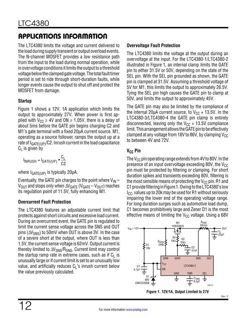
The LTC4380 limits the voltage and current delivered to the load during supply transient or output overload events. The N-channel MOSFET provides a low resistance path from the input to the load during normal operation, while in overvoltage conditions it limits the output to a threshold voltage below the clamped gate voltage. The total fault timer period is set to ride through short-duration faults, while longer events cause the output to shut off and protect the MOSFET from damage.
Startup
Figure 1 shows a 12V, 1A application which limits the output to approximately 27V. When power is first ap-plied with VCC ≥ 4V and ON ≥ 1.05V, there is a delay of about 5ms before the GATE pin begins charging C2 and M1’s gate terminal with a fixed 20µA current source. M1, operating as a source follower, ramps the output up at a rate of IGATE(UP)/C2. Inrush current in the load capacitance CL is given by
IINRUSH = IGATE(UP) •
CLC2
where IGATE(UP) is typically 20µA.
Eventually, the GATE pin charges to the point where VIN ≈ VOUT and stops only when ∆VGATE (VGATE – VOUT) reaches its regulation point of 11.5V, fully enhancing M1.
Overcurrent Fault Protection
The LTC4380 features an adjustable current limit that protects against short circuits and excessive load current. During an overcurrent event, the GATE pin is regulated to limit the current sense voltage across the SNS and OUT pins (∆VSNS) to 50mV when OUT is above 3V. In the case of a severe short at the output, where OUT is less than 1.5V, the current sense voltage is 62mV. Output current is thereby limited to ∆VSNS/RSNS. Current limit may control the startup ramp rate in extreme cases, such as if CL is unusually large or if current limit is set to an unusually low value, and artificially reduces CL’s inrush current below the value previously calculated.
APPLICATIONS INFORMATIONOvervoltage Fault Protection
The LTC4380 limits the voltage at the output during an overvoltage at the input. For the LTC4380-1/LTC4380-2 illustrated in Figure 1, an internal clamp limits the GATE pin to either 31.5V or 50V, depending on the state of the SEL pin. With the SEL pin grounded as shown, the GATE pin is clamped at 31.5V. Assuming a threshold voltage of 5V for M1, this limits the output to approximately 26.5V. Tying the SEL pin high causes the GATE pin to clamp at 50V, and limits the output to approximately 45V.
The GATE pin may also be limited by the compliance of the internal 20µA current source, to VCC + 13.5V. In the LTC4380-3/LTC4380-4 the GATE pin clamp is entirely disconnected, leaving only the VCC + 13.5V compliance limit. This arrangement allows the GATE pin to be effectively clamped at any voltage from 18V to 86V, by clamping VCC to between 4V and 72V.
VCC Pin
The VCC pin operating range extends from 4V to 80V. In the presence of an input overvoltage exceeding 80V, the VCC pin must be protected by filtering or clamping. For short duration spikes and transients exceeding 80V, filtering is the most sensible means of protecting the VCC pin. R1 and C1 provide filtering in Figure 1. Owing to the LTC4380’s low ICC, values up to 20k may be used for R1 without seriously impairing the lower end of the operating voltage range. For long duration surges such as automotive load dump, C1 becomes prohibitively large and Zener D1 is the most effective means of limiting the VCC voltage. Using a 68V
D168V
CMHZ5266B
C14.7µF
R233Ω
R310Ω
R110k
OUTVIN = 12V
C247nF
RDRN249k
RSNS20mΩ
M1FDB33N25
GATEDRN SNS OUT
VCC
ONSELTMR
LTC4380-2
GND
4380 F01
CL22µF
CTMR8.2µF
Figure 1. 12V/1A, Output Limited to 27V
LTC4380
13Rev. C
For more information www.analog.com
APPLICATIONS INFORMATIONZener assures that D1 will not override the internal GATE pin clamp in the LTC4380-1 and LTC4380-2 devices. For the LTC4380-3 and LTC4380-4, the VCC operating range extends from 4V to 72V. Since the GATE pin is regulated to VOUT + 11.5V, D1 is chosen to achieve the desired output clamping effect while at the same time keeping the VCC pin within its 4V to 72V range.
Fault Timer Overview
Overvoltage and overcurrent conditions, and high VDS conditions in M1 are limited in duration by an adjustable fault timer. A capacitor at the TMR pin (CTMR) sets the delay time before a fault condition is reported at the FLT pin and M1 is turned off. CTMR also sets the cool down time before M1 is permitted to turn back on for the LTC4380-2 and LTC4380-4 auto retry versions. The LTC4380-1 and LTC4380-3 versions simply latch off at the end of the timer delay. A 10V or higher rated X7R capacitor is recommended for CTMR to minimize temperature and voltage sensitivity.
Fault timing starts as soon as the input power is applied with the part in the on condition, or when the part is turn on after application of power. A 1.5µA current is gener-ated to pull up the TMR pin when the voltage across the MOSFET is higher than 0.7V. The timer speeds up with an additional current that varies with the power dissipated in the MOSFET, M1. The power dissipation is the product of the voltage across the MOSFET (VDS) and the current flowing through it (ID). VDS is inferred from the voltage drop across the drain pin resistor, RDRN, while ∆VSNS represents ID.
At initial power-up, the 1.5µA pilot current charges the TMR pin capacitor because the input supply is, at least for a short time, more than 0.7V above the output voltage. When the output rises to within 0.7V of the input supply voltage, the pull-up current disappears and an internal 2µA current source discharges the TMR pin capacitor. The capacitor must be sized to ride through the initial start-up interval for successful power-up.
In the presence of a sustained fault, the timer current charges the TMR pin to 1.215V. At this point the FLT pin pulls low to indicate a fault condition and the GATE pin pulls low, shutting off the MOSFET. After faulting off, the timer enters the cool down phase. At the end of the cool down period
the LTC4380-1/LTC4380-3 remain off until manually reset, while the LTC4380-2/LTC4380-4 automatically restart.
Fault Timer Operation in Overvoltage
During an overvoltage condition, where the MOSFET’s VDS exceeds 0.7V, the TMR pin charges from 0V to 1.215V with a current that varies principally as a function of VDS and ID. VDS is inferred from the current flowing in the DRN pin resistor, RDRN, while the voltage difference between the SNS and OUT pins (∆VSNS) represents the MOSFET current, ID.
The TMR pin current is given by
ITMR = 1.5 • 10–6A + 0.0917
AV
⎡
⎣⎢
⎤
⎦⎥ • ΔVSNS • IDRN
Where 1.5 • 10–6A is the minimum TMR current and 0.0917√A/V is the gain term of the multiplier.
Substituting for ∆VSNS and IDRN
ITMR = 1.5 • 10–6A + 0.0917
AV
⎡
⎣⎢
⎤
⎦⎥ • ID • VDS
RSNS
RDRN
When TMR reaches 1.215V, the FLT pin pulls low and the MOSFET is turned off and allowed to cool for an extended period. The total elapsed time between the onset of output clamping and turning off is given by:
tTMR = VTMR(F) •
CTMRITMR
Because ITMR is a function of VDS and ID, the exact time spent in overvoltage before turning off depends upon the input waveform and the load current.
Fault Timer Operation in Overcurrent
TMR pin behavior in overcurrent is substantially the same as in overvoltage. In the presence of an overcurrent condi-tion when the LTC4380 regulates the output current, the TMR pin charges from 0V to 1.215V with a current that varies principally as a function of the power dissipated in the MOSFET. In addition to the variable current, an ad-ditional 27µA hastens timeout in a low impedance short where the output is less than 1.5V. This additional current is reduced to 7µA when VOUT is above 3V.
LTC4380
14Rev. C
For more information www.analog.com
APPLICATIONS INFORMATIONThe TMR pin current with VOUT less than 1.5V is given by
ITMR = (27 + 1.5) • 10–6A + 0.0917A
V
⎡
⎣⎢
⎤
⎦⎥ •
ID • VDS RSNS
RDRN
Where 27 • 10–6A is the extra TMR current during over-current condition.
And with VOUT above 3V
ITMR = (7 + 1.5) • 10–6A + 0.0917A
V
⎡
⎣⎢
⎤
⎦⎥ •
ID • VDS RSNS
RDRN
Where 7 • 10–6A is the extra TMR current during overcur-rent condition.
When TMR reaches 1.215V, the FLT pin pulls low and the MOSFET is turned off and allowed to cool for an extended period. The total elapsed time between the onset of output clamping and turning off is given by
tTMR = VTMR(F) •
CTMRITMR
Because ITMR is a function of VDS and ID, the exact time spent in overcurrent before turning off depends upon the input waveform, the output voltage and the time required for the output current to come into regulation.
Cool Down Phase
Cool down behavior is the same whether initiated by overvoltage or overcurrent. During the cool down phase, the timer continues to charge from 1.215V to 3.4V with 2µA, and then discharge back down to 1.215V with 2µA. This cycle repeats 14 times and at the 15th cycle the TMR pin is pulled all the way to ground. The total cool down time is given by:
tCOOL = CTMR
15 • 4.37V + (1.215V – 0.1V)2µA
Up to this point the operation of the LTC4380-1/LTC4380-3 and LTC4380-2/LTC4380-4 is the same. Behavior at the end of the cool down phase is entirely different.
At the end of the cool down phase, when TMR crosses the 100mV reset threshold, the LTC4380-1/LTC4380-3 remain latched off and FLT remains low. They may be restarted by pulling the ON pin low for at least 100µs or by cycling the power supply. The cool down phase may be interrupted at anytime by pulling the ON pin low for at least 10ms/µF of CTMR; the LTC4380-1/LTC4380-3 will restart when ON goes high. The LTC4380-2/LTC4380-4 will automatically retry at the end of the cool down phase without cycling the ON pin and the cool down phase may be interrupted by pulling the ON pin low for at least 10ms/µF of CTMR.
For both versions, the FLT pin goes high in shutdown and is cleared high when power is first applied to VCC. If FLT is set low, it can be reset during the cool down phase by pulling the ON pin low for at least 10ms/µF of CTMR.
Supply Transient Protection
The LTC4380 is tested to operate to 72V and guaranteed to be safe from damage up to 80V. Voltage transients above 80V may cause permanent damage. During a short-circuit condition, the large change in current flowing through power supply traces and associated wiring can cause induc-tive voltage transients which can exceed 80V. To minimize the voltage transients, minimize the power trace parasitic inductance by using short, wide traces. An RC filter at the VCC pin is an effective measure against voltage spikes.
Another way to limit transients to less than 80V at the VCC pin is to use a small Zener diode and a resistor, D1 and R1 in Figure 1. The Zener diode limits the voltage at the pin while the resistor limits the current through the diode to a safe level during the surge. However, D1 can be omitted if the filtered voltage at the VCC pin, due to R1 and C1, stays below 80V. The inclusion of R1 in series with the VCC pin modestly increases the minimum required voltage at VIN due to the extra voltage drop across it from the small VCC current of the LTC4380 and the leakage current of D1.
A total bulk capacitance of at least 22µF low ESR elec-trolytic or ceramic is required close to the source pin of MOSFET M1.
LTC4380
15Rev. C
For more information www.analog.com
APPLICATIONS INFORMATIONMOSFET Selection
The LTC4380 drives an N-channel MOSFET to carry the load current. The important features of the MOSFET are on-resistance RDS(ON), the maximum drain-source voltage V(BR)DSS, the threshold voltage, and the safe operating area (SOA).
The maximum allowable drain-source voltage must be higher than the peak supply voltage. If the output is off or shorted to ground during an overvoltage event, the full supply voltage will appear across the MOSFET.
The gate drive for the MOSFET is guaranteed to be more than 10V and less than 14V above the OUT pin for those applications with VCC higher than 8V. This allows the use of a standard threshold voltage N-channel MOSFET. For systems with steady state VCC less than 8V, a logic level MOSFET is required since the gate drive can be as low as 5V.
The SOA of the MOSFET must encompass all fault condi-tions. In normal operation the MOSFET is fully on, dissipat-ing very little power. But during overvoltage or overcurrent faults, the GATE pin is either clamped to limit the output voltage or controlled to regulate the current through the MOSFET. Large current and high voltage drop across the MOSFET can coexist and dissipate significant power in these cases. The SOA curves of the MOSFET must be considered carefully in conjunction with the selection of the fault timer capacitor.
Transient Stress in the MOSFET
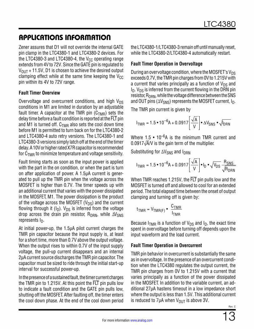
During an overvoltage event, the LTC4380 clamps the gate of the pass MOSFET to limit the output voltage at an acceptable level. The load circuitry may continue operating throughout this interval, but only at the expense of dissipa-tion in the MOSFET pass device. MOSFET dissipation or stress is a function of the input voltage waveform, output voltage and load current. The MOSFET must be sized to survive this stress.
Most transient event specifications use the prototypi-cal waveshape shown in Figure 2, comprising a linear ramp of rise time tr, reaching a peak voltage of VPK and exponentially decaying back to VIN with a time constant of τ. A common automotive transient specification has constants of tr = 10µs, VPK = 80V and τ = 1ms. A surge
condition known as load dump commonly has constants of tr = 5ms, VPK = 60V and τ = 200ms.
MOSFET stress is the result of power dissipated within the device. For long duration surges of 100ms or more, stress is increasingly dominated by heat transfer out of the package; this is a matter of device packaging and mount-ing, and heat sink thermal mass. This is best analyzed by simulation, using the MOSFET thermal model.
For short duration transients of less than 100ms, MOSFET survival is a matter of safe operating area (SOA), an intrinsic property of the MOSFET. SOA quantifies the time required at any given condition of VDS and ID to raise the junction temperature of the MOSFET to its rated maximum. MOSFET SOA can be expressed in units of watt-squared-seconds (P2t). This figure is essentially constant for intervals of less than 100ms for any given device type, and rises to infinity under DC operating conditions. Destruction mechanisms other than bulk die temperature distort the lines of an accurately drawn SOA graph so that P2t is not the same for all combinations of ID and VDS. In particular P2t tends to degrade as VDS approaches the maximum rating, rendering some devices useless for absorbing energy above a certain voltage.
Calculating Transient Stress
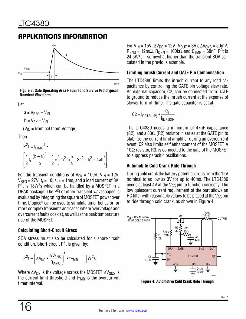
To select a MOSFET suitable for any given application, the SOA stress must be calculated or simulated for each input transient which shall not interrupt operation. It is then a simple matter to choose a device which has adequate SOA to survive the maximum calculated stress. P2t for a prototypical transient waveform is calculated as follows (Figure 3):
Figure 2. Prototypical Transient Waveform
VPK
τ
VIN
4380 F02tr
LTC4380
16Rev. C
For more information www.analog.com
C14.7µF
R310Ω
R110k
OUTPUTVIN = 12V, NOMINAL3V AT COLD CRANK
C247nF
RDRN249k
RSNS10mΩM1
GATEDRN SNS OUT
VCC
ONSELTMR
LTC4380
GND
4380 F04
CTMR220nF
FLT
R233Ω
APPLICATIONS INFORMATION
Let
a = VREG – VIN
b = VPK – VIN
(VIN = Nominal Input Voltage)
Then
P2t = ILOAD2 •
13
trb – a( )3
b+
12
τ 2a2 lnba
+ 3a2 + b2 – 4ab⎛
⎝⎜
⎞
⎠⎟
⎡
⎣
⎢⎢
⎤
⎦
⎥⎥
For the transient conditions of VPK = 100V, VIN = 12V, VREG = 27V, tr = 10µs, τ = 1ms, and a load current of 3A, P2t is 18W2s which can be handled by a MOSFET in a DPAK package. The P2t of other transient waveshapes is evaluated by integrating the square of MOSFET power over time. LTspice® can be used to simulate timer behavior for more complex transients and cases where overvoltage and overcurrent faults coexist, as well as the peak temperature rise of the MOSFET.
Calculating Short-Circuit Stress
SOA stress must also be calculated for a short-circuit condition. Short-circuit P2t is given by:
P2t = ΔVDS •
ΔVSNSRSNS
⎛
⎝⎜
⎞
⎠⎟
2
• tTMR W2s⎡⎣
⎤⎦
Where ∆VDS is the voltage across the MOSFET, ∆VSNS is the current limit threshold and tTMR is the overcurrent timer interval. Figure 4. Automotive Cold Crank Ride Through
For VIN = 15V, ∆VDS = 12V (VOUT = 3V), ∆VSNS = 50mV, RSNS = 12mΩ, RDRN = 100kΩ and CTMR = 68nF, P2t is 24.5W2s – somewhat higher than the transient SOA cal-culated in the previous example.
Limiting Inrush Current and GATE Pin Compensation
The LTC4380 limits the inrush current to any load ca-pacitance by controlling the GATE pin voltage slew rate. An external capacitor, C2, can be connected from GATE to ground to reduce the inrush current at the expense of slower turn-off time. The gate capacitor is set at:
C2 = IGATE(UP) •
CLIINRUSH
The LTC4380 needs a minimum of 47nF capacitance (C2) and a 33Ω (R2) resistor in series at the GATE pin to stabilize the current limit amplifier during an overcurrent event. C2 also limits self enhancement of the MOSFET. A 10Ω resistor, R3, is connected to the gate of the MOSFET to suppress parasitic oscillations.
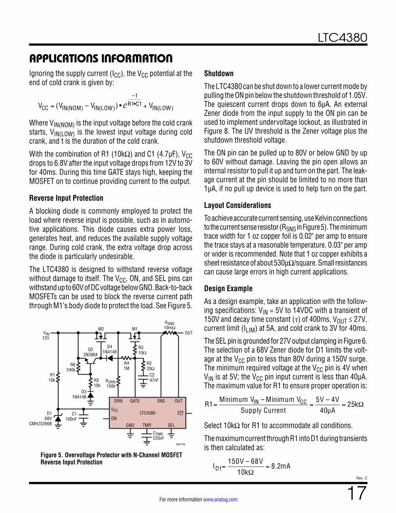
Automobile Cold Crank Ride Through
During cold crank the battery potential drops from the 12V nominal to as low as 3V for up to 40ms. The LTC4380 needs at least 4V at the VCC pin to function correctly. The low quiescent current requirement of the part allows an RC filter with reasonable values to be placed at the VCC pin to ride through cold crank, as shown in Figure 4.
Figure 3. Safe Operating Area Required to Survive Prototypical Transient Waveform
VPK
τ
VIN
4380 F03
VREG
tr
LTC4380
17Rev. C
For more information www.analog.com
Figure 5. Overvoltage Protector with N-Channel MOSFET Reverse Input Protection
D168V
CMHZ5266B
R310Ω
R110k
OUTVIN12V
C247nFR5
10kD3
1N4148
D41N4148
RSNS10mΩM1M2
Q32N3904
R233Ω
R6240k
GATEDRN SNS OUT
VCC
ONSELTMR
LTC4380
GND
4380 F05
C1100nF
CTMR220nF
FLT
RDRN150k
R41M
Ignoring the supply current (ICC), the VCC potential at the end of cold crank is given by:
VCC = (VIN(NOM) – VIN(LOW)) • e
– tR1•C1 + VIN(LOW)
Where VIN(NOM) is the input voltage before the cold crank starts, VIN(LOW) is the lowest input voltage during cold crank, and t is the duration of the cold crank.
With the combination of R1 (10kΩ) and C1 (4.7µF), VCC drops to 6.8V after the input voltage drops from 12V to 3V for 40ms. During this time GATE stays high, keeping the MOSFET on to continue providing current to the output.
Reverse Input Protection
A blocking diode is commonly employed to protect the load where reverse input is possible, such as in automo-tive applications. This diode causes extra power loss, generates heat, and reduces the available supply voltage range. During cold crank, the extra voltage drop across the diode is particularly undesirable.
The LTC4380 is designed to withstand reverse voltage without damage to itself. The VCC, ON, and SEL pins can withstand up to 60V of DC voltage below GND. Back-to-back MOSFETs can be used to block the reverse current path through M1’s body diode to protect the load. See Figure 5.
Shutdown
The LTC4380 can be shut down to a lower current mode by pulling the ON pin below the shutdown threshold of 1.05V. The quiescent current drops down to 6µA. An external Zener diode from the input supply to the ON pin can be used to implement undervoltage lockout, as illustrated in Figure 8. The UV threshold is the Zener voltage plus the shutdown threshold voltage.
The ON pin can be pulled up to 80V or below GND by up to 60V without damage. Leaving the pin open allows an internal resistor to pull it up and turn on the part. The leak-age current at the pin should be limited to no more than 1µA, if no pull up device is used to help turn on the part.
Layout Considerations
To achieve accurate current sensing, use Kelvin connections to the current sense resistor (RSNS in Figure 5). The minimum trace width for 1 oz copper foil is 0.02" per amp to ensure the trace stays at a reasonable temperature. 0.03" per amp or wider is recommended. Note that 1 oz copper exhibits a sheet resistance of about 530µΩ/square. Small resistances can cause large errors in high current applications.
Design Example
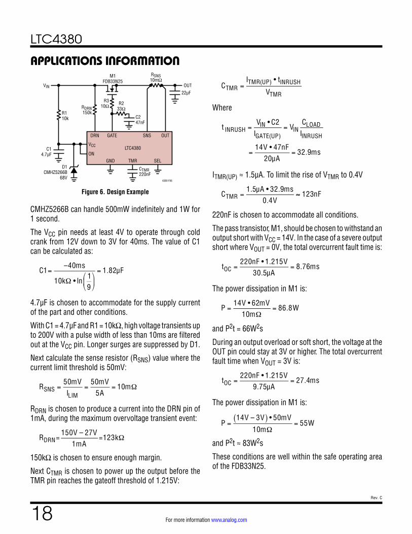
As a design example, take an application with the follow-ing specifications: VIN = 5V to 14VDC with a transient of 150V and decay time constant (τ) of 400ms, VOUT ≤ 27V, current limit (ILIM) at 5A, and cold crank to 3V for 40ms.
The SEL pin is grounded for 27V output clamping in Figure 6. The selection of a 68V Zener diode for D1 limits the volt-age at the VCC pin to less than 80V during a 150V surge. The minimum required voltage at the VCC pin is 4V when VIN is at 5V; the VCC pin input current is less than 40µA. The maximum value for R1 to ensure proper operation is:
R1=
Minimum VIN – Minimum VCCSupply Current
=5V – 4V
40µA= 25kΩ
Select 10kΩ for R1 to accommodate all conditions.
The maximum current through R1 into D1 during transients is then calculated as:
ID1=
150V – 68V10kΩ
= 8.2mA
APPLICATIONS INFORMATION
LTC4380
18Rev. C
For more information www.analog.com
APPLICATIONS INFORMATION
CMHZ5266B can handle 500mW indefinitely and 1W for 1 second.
The VCC pin needs at least 4V to operate through cold crank from 12V down to 3V for 40ms. The value of C1 can be calculated as:
C1=–40ms
10kΩ • ln19
⎛
⎝⎜
⎞
⎠⎟
= 1.82µF
4.7µF is chosen to accommodate for the supply current of the part and other conditions.
With C1 = 4.7µF and R1 = 10kΩ, high voltage transients up to 200V with a pulse width of less than 10ms are filtered out at the VCC pin. Longer surges are suppressed by D1.
Next calculate the sense resistor (RSNS) value where the current limit threshold is 50mV:
RSNS =
50mVILIM
=50mV
5A= 10mΩ
RDRN is chosen to produce a current into the DRN pin of 1mA, during the maximum overvoltage transient event:
RDRN=
150V – 27V1mA
=123kΩ
150kΩ is chosen to ensure enough margin.
Next CTMR is chosen to power up the output before the TMR pin reaches the gateoff threshold of 1.215V:
CTMR =
ITMR(UP) • tINRUSH
VTMR
Where
t INRUSH =VIN • C2
IGATE(UP)= VIN
CLOADIINRUSH
=14V • 47nF
20µA= 32.9ms
ITMR(UP) ≈ 1.5µA. To limit the rise of VTMR to 0.4V
CTMR =
1.5µA • 32.9ms0.4V
≈ 123nF
220nF is chosen to accommodate all conditions.
The pass transistor, M1, should be chosen to withstand an output short with VCC = 14V. In the case of a severe output short where VOUT = 0V, the total overcurrent fault time is:
tOC =
220nF • 1.215V30.5µA
= 8.76ms
The power dissipation in M1 is:
P =
14V • 62mV10mΩ
= 86.8W
and P2t = 66W2s
During an output overload or soft short, the voltage at the OUT pin could stay at 3V or higher. The total overcurrent fault time when VOUT = 3V is:
tOC =
220nF • 1.215V9.75µA
= 27.4ms
The power dissipation in M1 is:
P =
14V – 3V( ) • 50mV
10mΩ= 55W
and P2t ≈ 83W2s
These conditions are well within the safe operating area of the FDB33N25.
D1CMHZ5266B
68V
C14.7µF
R233Ω
R310Ω
R110k
OUTVIN
C247nF
RDRN150k
RSNS10mΩ
M1FDB33N25
GATEDRN SNS OUT
VCC
ONSELTMR
LTC4380
GND
4380 F06
CTMR220nF
22µF
Figure 6. Design Example
LTC4380
19Rev. C
For more information www.analog.com
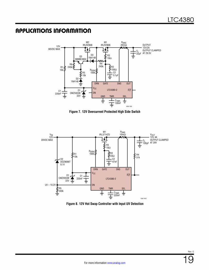
Figure 7. 12V Overcurrent Protected High Side Switch
D1CMZ5933B
22V
R310Ω
R4240kR1
10k
OUTPUT12V/2AOUTPUT CLAMPEDAT 29.5V
12V80VDC MAX
C20.1µF
R510k
D21N4148
D31N4148
RSNS20mΩ
M1IRLR2908
M2IRLR2908
Q3MMBE3904
R6240k
GATEDRN SNS OUT
VCC
ONSELTMR
LTC4380-2
GND
4380 TA02
C1220nF
CL22µF
CTMR100nF
FLT
RDRN100k
R2150Ω
Figure 8. 12V Hot Swap Controller with Input UV Detection
D1CMZ5933B
22V
R310Ω
R110k
VOUT12V, 4AOUTPUT CLAMPEDAT 29V
VIN12V
20VDC MAX
RSNS10mΩ
M1IRL3714ZS
R5240k
UV ≈ 10.2V
R451k
GATEDRN SNS OUTVCC
ONSELTMR
LTC4380-2
GND
4380 TA03
C1220nF
CL100µF
CTMR220nF
FLT
D2DDZ9696T9.1V
RDRN100k
C247nF
R233Ω
APPLICATIONS INFORMATION
LTC4380
20Rev. C
For more information www.analog.com
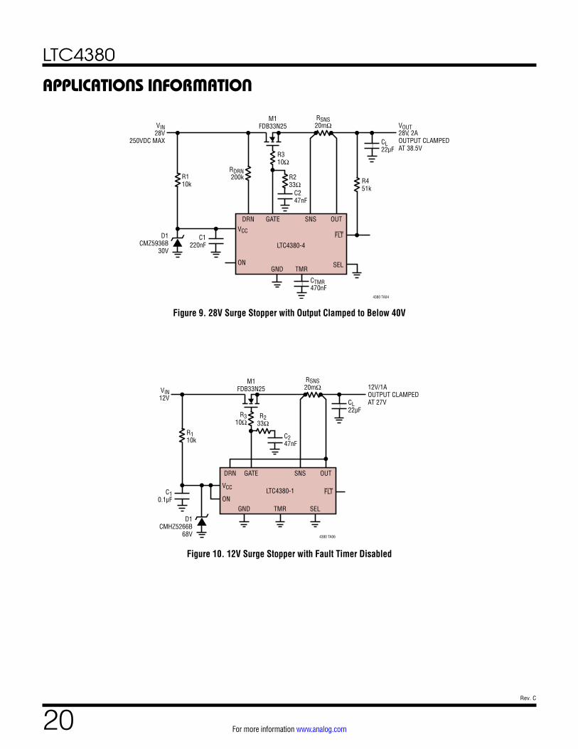
Figure 9. 28V Surge Stopper with Output Clamped to Below 40V
Figure 10. 12V Surge Stopper with Fault Timer Disabled
D1CMZ5936B
30V
R310Ω
R110k
VOUT28V, 2AOUTPUT CLAMPEDAT 38.5V
VIN28V
250VDC MAX
RSNS20mΩ
M1FDB33N25
R451k
GATEDRN SNS OUTVCC
ON SELTMR
LTC4380-4
GND
4380 TA04
C1220nF
CL22µF
CTMR470nF
FLT
RDRN200k
C247nF
R233Ω
M1FDB33N25
D1CMHZ5266B
68V
C10.1µF
R310Ω
R233Ω
R110k
12V/1AOUTPUT CLAMPED AT 27V
VIN12V
C247nF
RSNS20mΩ
GATEDRN SNS OUT
VCC
ONFLT
SELTMR
LTC4380-1
GND
4380 TA06
CL22µF
APPLICATIONS INFORMATION
LTC4380
21Rev. C
For more information www.analog.com
PACKAGE DESCRIPTIONDD Package
10-Lead Plastic DFN (3mm × 3mm)(Reference LTC DWG # 05-08-1699 Rev C)
3.00 ±0.10(4 SIDES)
NOTE:1. DRAWING TO BE MADE A JEDEC PACKAGE OUTLINE M0-229 VARIATION OF (WEED-2). CHECK THE LTC WEBSITE DATA SHEET FOR CURRENT STATUS OF VARIATION ASSIGNMENT2. DRAWING NOT TO SCALE3. ALL DIMENSIONS ARE IN MILLIMETERS4. DIMENSIONS OF EXPOSED PAD ON BOTTOM OF PACKAGE DO NOT INCLUDE MOLD FLASH. MOLD FLASH, IF PRESENT, SHALL NOT EXCEED 0.15mm ON ANY SIDE5. EXPOSED PAD SHALL BE SOLDER PLATED6. SHADED AREA IS ONLY A REFERENCE FOR PIN 1 LOCATION ON THE TOP AND BOTTOM OF PACKAGE
0.40 ±0.10
BOTTOM VIEW—EXPOSED PAD
1.65 ±0.10(2 SIDES)
0.75 ±0.05
R = 0.125TYP
2.38 ±0.10(2 SIDES)
15
106
PIN 1TOP MARK
(SEE NOTE 6)
0.200 REF
0.00 – 0.05
(DD) DFN REV C 0310
0.25 ±0.05
2.38 ±0.05(2 SIDES)
RECOMMENDED SOLDER PAD PITCH AND DIMENSIONS
1.65 ±0.05(2 SIDES)2.15 ±0.05
0.50BSC
0.70 ±0.05
3.55 ±0.05
PACKAGEOUTLINE
0.25 ±0.050.50 BSC
DD Package10-Lead Plastic DFN (3mm × 3mm)
(Reference LTC DWG # 05-08-1699 Rev C)
PIN 1 NOTCHR = 0.20 OR0.35 × 45°CHAMFER
LTC4380
22Rev. C
For more information www.analog.com
PACKAGE DESCRIPTIONMS Package
10-Lead Plastic MSOP(Reference LTC DWG # 05-08-1661 Rev F)
MSOP (MS) 0213 REV F
0.53 ±0.152(.021 ±.006)
SEATINGPLANE
0.18(.007)
1.10(.043)MAX
0.17 – 0.27(.007 – .011)
TYP
0.86(.034)REF
0.50(.0197)
BSC
1 2 3 4 5
4.90 ±0.152(.193 ±.006)
0.497 ±0.076(.0196 ±.003)
REF8910 7 6
3.00 ±0.102(.118 ±.004)
(NOTE 3)
3.00 ±0.102(.118 ±.004)
(NOTE 4)
NOTE:1. DIMENSIONS IN MILLIMETER/(INCH)2. DRAWING NOT TO SCALE3. DIMENSION DOES NOT INCLUDE MOLD FLASH, PROTRUSIONS OR GATE BURRS. MOLD FLASH, PROTRUSIONS OR GATE BURRS SHALL NOT EXCEED 0.152mm (.006") PER SIDE4. DIMENSION DOES NOT INCLUDE INTERLEAD FLASH OR PROTRUSIONS. INTERLEAD FLASH OR PROTRUSIONS SHALL NOT EXCEED 0.152mm (.006") PER SIDE5. LEAD COPLANARITY (BOTTOM OF LEADS AFTER FORMING) SHALL BE 0.102mm (.004") MAX
0.254(.010) 0° – 6° TYP
DETAIL “A”
DETAIL “A”
GAUGE PLANE
5.10(.201)MIN
3.20 – 3.45(.126 – .136)
0.889 ±0.127(.035 ±.005)
RECOMMENDED SOLDER PAD LAYOUT
0.305 ±0.038(.0120 ±.0015)
TYP
0.50(.0197)
BSC
0.1016 ±0.0508(.004 ±.002)
MS Package10-Lead Plastic MSOP
(Reference LTC DWG # 05-08-1661 Rev F)
LTC4380
23Rev. C
For more information www.analog.com
Information furnished by Analog Devices is believed to be accurate and reliable. However, no responsibility is assumed by Analog Devices for its use, nor for any infringements of patents or other rights of third parties that may result from its use. Specifications subject to change without notice. No license is granted by implication or otherwise under any patent or patent rights of Analog Devices.
REVISION HISTORYREV DATE DESCRIPTION PAGE NUMBER
A 08/16 Updated specification limits: IOUT ON, ∆VSNS at OUT = 6V/12V.TMR pin function: Added recommendation for capacitor rating and type.
3, 47
B 06/17 Clarified pin conditions for Electrical CharacteristicsUpdated conditions for ITMR(UP) Overvoltage and Retry Duty Cycle Overcurrent specifications
45
C 06/19 Added AEC-Q100 qualification and “W” part numbers 1, 3
LTC4380
24Rev. C
For more information www.analog.com
06/19www.analog.com
ANALOG DEVICES, INC. 2016–2019
RELATED PARTS
TYPICAL APPLICATION
PART NUMBER DESCRIPTION COMMENTS
LT4356 Surge Stopper with Current Limit 4V to 80V Operation; 100V Protection; DFN-12, MSOP-10 and SO-16 Packages
LTC4359 Ideal Diode Controller 4V to 80V Operation, –40V Input Protection, DFN-8 and MSOP-8 Packages
LTC4361 Overvoltage/Overcurrent Protection Controller 2.5V to 5.5V Operation, 80V Protection, TSOT-8 and DFN-8 Packages
LT4363 Surge Stopper with Current Limit 4V to 80V Operation; >100V Protection; DFN-12, MSOP-12 and SO-16 Packages
LTC4364 Surge Stopper with Ideal Diode 4V to 80V Operation; –40V to >100V Protection; DFN-14, MSOP-16 and SO-16 Packages
LTC4365 OV, UV and Reverse Input Protection Controller 2.5V to 34V Operation, –40V to 60V Protection, DFN-8 and TSOT-8 Packages
LTC4366 High Voltage Surge Stopper 9V to >500V Operation, Floating Topology, TSOT-8 and DFN-8 Packages
LTC4367 OV, UV and Reverse Input Protection Controller 2.5V to 60V Operation, –40V to 100V Protection, DFN-8 and MSOP-8 Packages
LTC4368 LTC4367 + Bidirectional Circuit Breaker ±50mV or +50mV/–3mV Circuit Breaker Thresholds; DFN-10, MSOP-10 Packages
LTC7860 Switching Surge Stopper 3.5V to 60V Operation, >100V Protection, MSOPE-12 Package
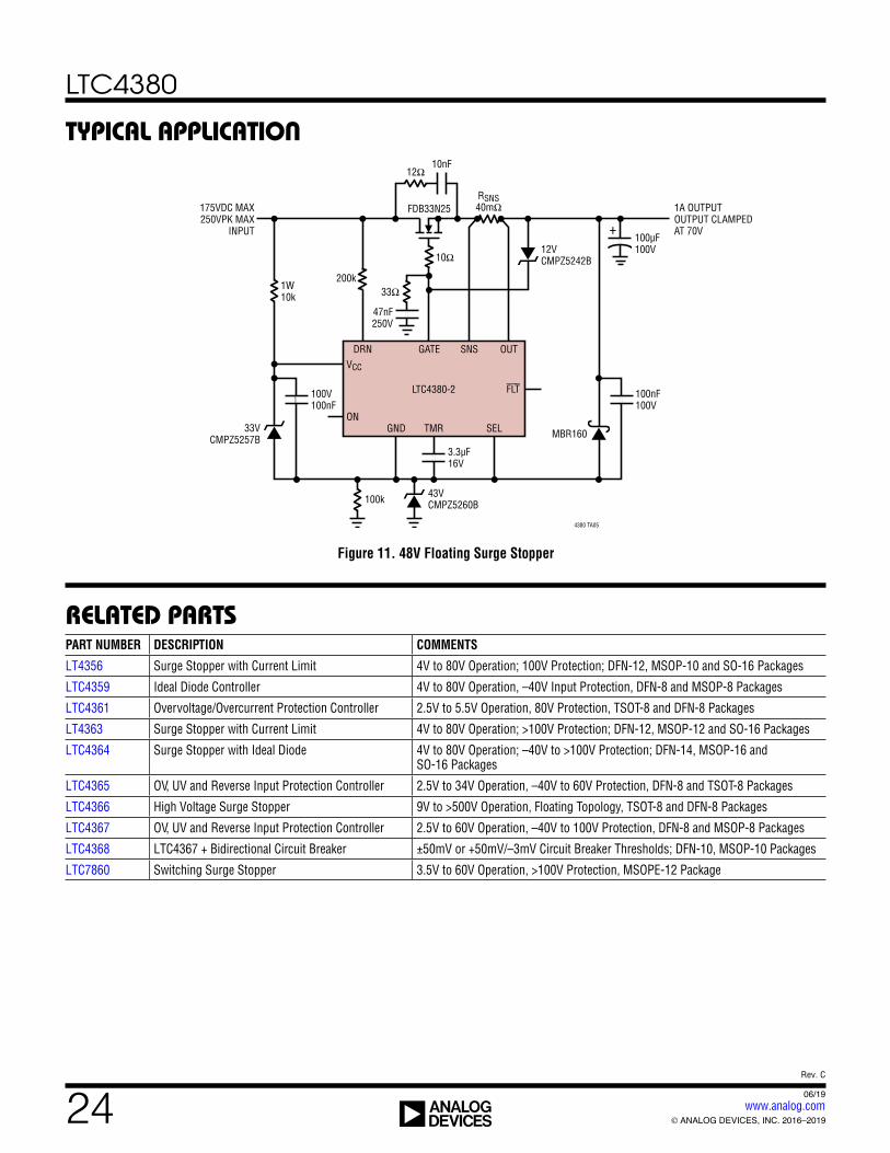
Figure 11. 48V Floating Surge Stopper
33VCMPZ5257B
12VCMPZ5242B10Ω
1W10k
1A OUTPUTOUTPUT CLAMPEDAT 70V
175VDC MAX250VPK MAX
INPUT
47nF250V
12Ω
RSNS40mΩFDB33N25
100k
GATEDRN SNS OUTVCC
ONSELTMR
LTC4380-2
GND
4380 TA05
100V100nF
100nF100V
100µF100V
3.3µF16V
FLT
MBR160
10nF
43VCMPZ5260B
200k
+
33Ω