Embed Size (px)
Citation preview
LTC3775
13775fa
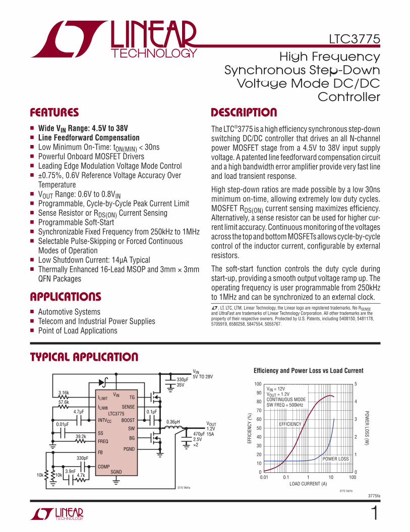
TYPICAL APPLICATION
FEATURES
APPLICATIONS
DESCRIPTION
High Frequency Synchronous Step-Down
Voltage Mode DC/DC Controller
The LTC®3775 is a high effi ciency synchronous step-down switching DC/DC controller that drives an all N-channel power MOSFET stage from a 4.5V to 38V input supply voltage. A patented line feedforward compensation circuit and a high bandwidth error amplifi er provide very fast line and load transient response.
High step-down ratios are made possible by a low 30ns minimum on-time, allowing extremely low duty cycles. MOSFET RDS(ON) current sensing maximizes effi ciency. Alternatively, a sense resistor can be used for higher cur-rent limit accuracy. Continuous monitoring of the voltages across the top and bottom MOSFETs allows cycle-by-cycle control of the inductor current, confi gurable by external resistors.
The soft-start function controls the duty cycle during start-up, providing a smooth output voltage ramp up. The operating frequency is user programmable from 250kHz to 1MHz and can be synchronized to an external clock.
n Wide VIN Range: 4.5V to 38Vn Line Feedforward Compensationn Low Minimum On-Time: tON(MIN) < 30nsn Powerful Onboard MOSFET Driversn Leading Edge Modulation Voltage Mode Control n ±0.75%, 0.6V Reference Voltage Accuracy Over
Temperaturen VOUT Range: 0.6V to 0.8VINn Programmable, Cycle-by-Cycle Peak Current Limitn Sense Resistor or RDS(ON) Current Sensingn Programmable Soft-Startn Synchronizable Fixed Frequency from 250kHz to 1MHzn Selectable Pulse-Skipping or Forced Continuous
Modes of Operation n Low Shutdown Current: 14μA Typicaln Thermally Enhanced 16-Lead MSOP and 3mm × 3mm
QFN Packages
n Automotive Systemsn Telecom and Industrial Power Suppliesn Point of Load Applications
L, LT, LTC, LTM, Linear Technology, the Linear logo are registered trademarks, No RSENSE and UltraFast are trademarks of Linear Technology Corporation. All other trademarks are the property of their respective owners. Protected by U.S. Patents, including 5408150, 5481178, 5705919, 6580258, 5847554, 5055767.
0.1μF
0.36μH
470μF2.5V×2
330μF35V
VIN5V TO 28V
VOUT1.2V15A
3775 TA01a
4.7μF
330pF
3.9nF
57.6k
39.2k
4.7k10k10k
3.16k
0.01μF
TGVIN
LTC3775
SGND
SENSE
ILIMT
ILIMB
INTVCC
SSBG
PGND
COMP
BOOST
SW
FREQ
FB
LOAD CURRENT (A)
30
EFF
ICIE
NC
Y (
%)
PO
WER
LO
SS
(W)
90
100
20
10
80
50
70
60
40
0.01 1 10 100
3775 TA01b
0
1
2
3
4
5
00.1
EFFICIENCY
POWER LOSS
VIN = 12VVOUT = 1.2VCONTINUOUS MODESW FREQ = 500kHz
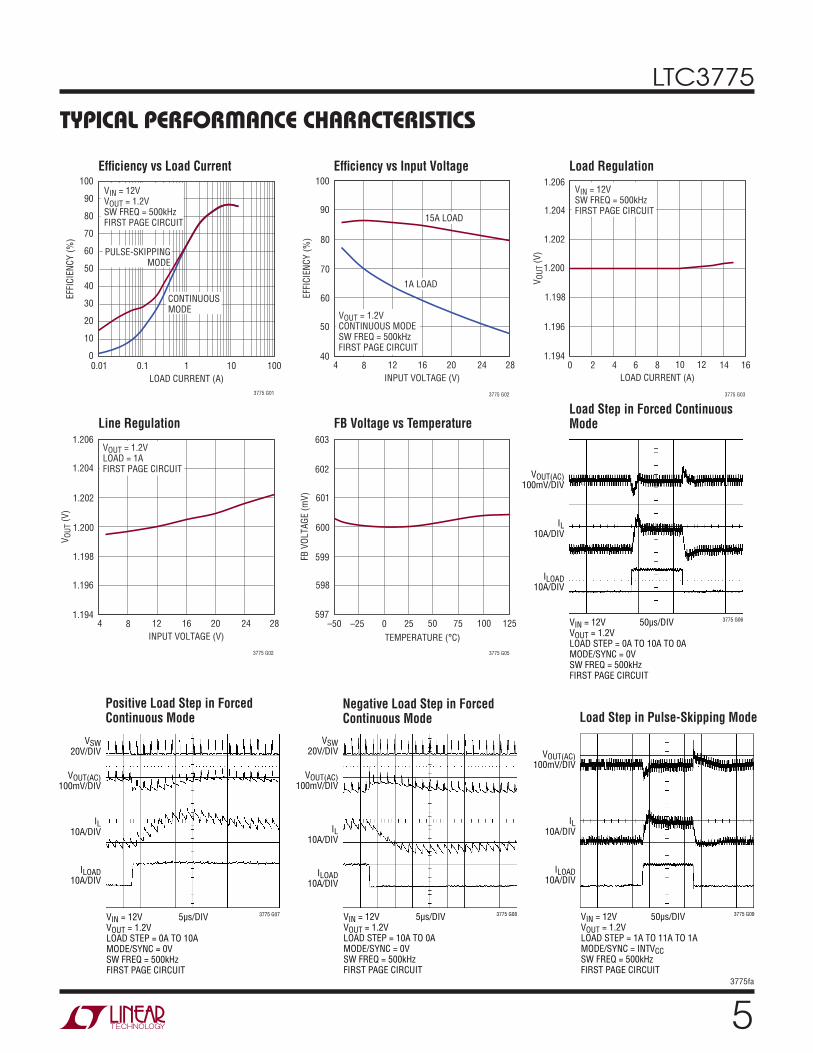
Effi ciency and Power Loss vs Load Current

LTC3775
23775fa
ABSOLUTE MAXIMUM RATINGSSupply Voltage VIN ......................................................... –0.3V to 40V BOOST ................................................... –0.3V to 46V BOOST-SW ............................................... –0.3V to 6V SW ............................................................ –5V to 40VILIMT .............................................................–0.3V to VIN
SENSE .............................................................–5V to VIN
INTVCC ......................................................... –0.3V to 6V
(Note 1)
16 15 14 13
5 6 7 8
TOP VIEW
UD PACKAGE16-LEAD (3mm 3mm) PLASTIC QFN
9
10
11
12
4
3
2
1ILIMT
ILIMB
FB
COMP
SW
VIN
SENSE
INTVCC
RU
N/SHDN
MO
DE/S
YN
C
BO
OS
T
TG
SS
FREQ
SG
ND
BG
17PGND
TJMAX = 125°C, θJA = 68°C/W, θJC = 4.2°C/W (NOTE 3)EXPOSED PAD (PIN 17) IS PGND, MUST BE SOLDERED TO PCB
12345678
MODE/SYNCRUN/SHDN
ILIMTILIMB
FBCOMP
SSFREQ
161514131211109
BOOSTTGSWVINSENSEINTVCCBGSGND
TOP VIEW
17PGND
MSE PACKAGE16-LEAD PLASTIC MSOP
TJMAX = 125°C, θJA = 40°C/W (NOTE 3)EXPOSED PAD (PIN 17) IS PGND, MUST BE SOLDERED TO PCB
PIN CONFIGURATION
ORDER INFORMATION
LEAD FREE FINISH TAPE AND REEL PART MARKING* PACKAGE DESCRIPTION TEMPERATURE RANGE
LTC3775EUD#PBF LTC3775EUD#TRPBF LDJK 16-Lead (3mm × 3mm) Plastic QFN –40°C to 85°C
LTC3775IUD#PBF LTC3775IUD#TRPBF LDJK 16-Lead (3mm × 3mm) Plastic QFN –40°C to 125°C
LTC3775EMSE#PBF LTC3775EMSE#TRPBF 3775 16-Lead Plastic MSOP –40°C to 85°C
LTC3775IMSE#PBF LTC3775IMSE#TRPBF 3775 16-Lead Plastic MSOP –40°C to 125°C
Consult LTC Marketing for parts specifi ed with wider operating temperature ranges. *The temperature grade is identifi ed by a label on the shipping container.
Consult LTC Marketing for information on non-standard lead based fi nish parts.
For more information on lead free part marking, go to: http://www.linear.com/leadfree/ For more information on tape and reel specifi cations, go to: http://www.linear.com/tapeandreel/
RUN/SHDN ................................................... –0.3V to 6VFB, MODE/SYNC ................................... –0.3V to INTVCC
FREQ, ILIMB, SS ..................................... –0.3V to INTVCC
INTVCC RMS Currents... .........................................50mAOperating Junction Temperature Range (Note 2) .................................................. –40°C to 125°CStorage Temperature Range ................... –65°C to 150°C

LTC3775
33775fa
ELECTRICAL CHARACTERISTICS
SYMBOL PARAMETER CONDITIONS MIN TYP MAX UNITS
Input Supply
VIN VIN Supply Voltage l 4.5 38 V
IVIN Input DC Supply Current VFB = 0.7V (Note 5)VRUN = 0V
3.514
mAμA
RUN/SHDN Pin
VRUN RUN/SHDN Pin Enable Threshold 1.19 1.22 1.25 V
VSHDN RUN/SHDN Pin Shutdown Threshold VRUN/SHDN Rising 0.74 V
VSHDN(HYST) RUN/SHDN Pin Shutdown Threshold Hysteresis 140 mV
IRUN RUN/SHDN Pin Source Current VRUN/SHDN = 0VVRUN/SHDN = 1.5V
–1–5
μAμA
Error Amplifi er
VFB Feedback Pin Voltagel
0.5970.5955
0.600 0.6030.6045
VV
ΔVFB Feedback Voltage Line Regulation 4.5V < VIN < 38V ±0.01 %/V
ΔVOUT Output Voltage Load Regulation 1V < VCOMP < 2V (Note 6) 0.01 0.1 %
IFB FB Pin Input Current VFB = 0.6V –50 50 nA
ICOMP COMP Pin Output Current Sourcing, VCOMP = 0VSinking, VCOMP = 2V
–0.51
–160
mAmA
f0dB Error Amplifi er Unity-Gain Crossover Frequency (Note 6) 25 MHz
Soft-Start
ISS SS Pin Source Current VSS = 0V –1 μA
RSS SS Pin Pull-Down Resistance in Current Limit 1.3 kΩ
Current Limit
ILIMB ILIMB Source Current VILIMB = 1V l –9 –10 –11 μA
ILIMT ILIMT Sink Current VILIMT = 12V l 90 100 110 μA
ISENSE SENSE Pin Input Current 1 μA
VILIMT(MAX) Topside Current Limit Threshold (VIN-SENSE) VILIMT = 0.1V l 90 100 110 mV
VILIMB(MAX) Bottom Side Current Limit Threshold (PGND-SW) VILIMB = 0.5V l 80 100 120 mV
INTVCC Low Dropout Voltage Regulator
INTVCC LDO Regulator Output Voltage 4.9 5.2 5.5 V
ΔVINTVCC(LINE) INTVCC Line Regulation 7.5V < VIN < 38V 0.01 %/V
ΔVINTVCC(LOAD) INTVCC Load Regulation ΔIINTVCC = 0mA to 20mA –1 –0.1 %
VDROPOUT INTVCC Regulator Dropout Voltage (VIN – VINTVCC) IINTVCC = 20mA 0.35 V
VUVLO INTVCC UVLO Voltage INTVCC RisingHysteresis
3.0 3.60.5
4.2 VV
The l denotes the specifi cations which apply over the full operating junction temperature range, otherwise specifi cations are at TA = 25°C (Note 2). VIN = 12V, VRUN = 5V, unless otherwise specifi ed.

LTC3775
43775fa
ELECTRICAL CHARACTERISTICS The l denotes the specifi cations which apply over the full operating junction temperature range, otherwise specifi cations are at TA = 25°C (Note 2). VIN = 12V, VRUN = 5V, unless otherwise specifi ed.
SYMBOL PARAMETER CONDITIONS MIN TYP MAX UNITS
Oscillator
fOSC Oscillator Frequency RSET = 39.2k l 425 500 575 kHz
fHIGH Maximum Oscillator Frequency l 1000 kHz
fLOW Minimum Oscillator Frequency l 250 kHz
fSYNC External Sync Frequency Range With Reference to Free Running –20 20 %
tON(MIN) TG Minimum On-Time (Notes 6, 8) VMODE/SYNC = 0V 30 ns
tOFF(MIN) TG Minimum Off-Time (Note 6) 300 ns
DCMAX Maximum TG Duty Cycle fOSC = 500kHz l 90 %
VMODE MODE/SYNC Threshold MODE/SYNC Rising 1.2 V
VMODE(HYST) MODE/SYNC Hysteresis 430 mV
RMODE/SYNC MODE/SYNC Input Resistance to SGND 50 kΩ
Driver
BG RUP Bottom Gate (BG) Pull-Up On-Resistance 2.5 Ω
TG RUP Top Gate (TG) Pull-Up On-Resistance 2.5 Ω
BG RDOWN Bottom Gate (BG) Pull-Down On-Resistance 1.0 Ω
TG RDOWN Top Gate (TG) Pull-Down On-Resistance 1.5 Ω
BG, TG t2D Bottom Gate Off to Top Gate On Delay Top Switch-On Delay Time
CL = 3300pF (Note 7) 15 ns
TG, BG t1D Top Gate Off to Bottom Gate On Delay Synchronous Switch-On Delay Time
CL = 3300pF (Note 7) 15 ns
Note 1: Stresses beyond those listed under Absolute Maximum Ratings
may cause permanent damage to the device. Exposure to any Absolute
Maximum Rating condition for extended periods may affect device
reliability and lifetime.
Note 2: The LTC3775 is tested under pulsed load conditions such that TJ ≈ TA.
The LTC3775E is guaranteed to meet specifi cations from 0°C to 85°C
junction temperature. Specifi cations over the –40°C to 125°C operating
junction temperature range are assured by design, characterization and
correlation with statistical process controls. The LTC3775I is guaranteed
over the –40°C to 125°C operating junction temperature range. Note that
the maximum ambient temperature consistent with these specifi cations
is determined by specifi c operating conditions in conjunction with board
layout, the rated package thermal impedance and other environmental
factors.
The junction temperature (TJ, in °C) is calculated from the ambient
temperature (TA, in °C) and power dissipation (PD, in Watts) according to
the formula:
TJ = TA + (PD • θJA), where θJA (in °C/W) is the package thermal
impedance.
Note 3: Failure to solder the exposed pad of the UD package to the PC
board will result in a thermal resistance much higher than 68°C/W.
Note 4: All currents into device pins are positive; all currents out of device
pins are negative. All voltages are referenced to ground unless otherwise
specifi ed.
Note 5: Supply current in normal operation is dominated by the current
needed to charge and discharge the external MOSFET gates. This current
will vary with supply voltage and the external MOSFETs used.
Note 6: Guaranteed by design, not subject to test.
Note 7: Rise and fall times are measured using 10% and 90% levels. Delay
and nonoverlap times are measured using 50% levels.
Note 8: The LTC3775 leading edge modulation architecture does not have
a minimum TG pulse width requirement. The TG minimum pulse width is
limited by the SW node rise and fall times.
LTC3775
53775fa
TYPICAL PERFORMANCE CHARACTERISTICS
Effi ciency vs Load Current Effi ciency vs Input Voltage Load Regulation
Line Regulation FB Voltage vs TemperatureLoad Step in Forced Continuous Mode
Positive Load Step in Forced Continuous Mode
Negative Load Step in Forced Continuous Mode Load Step in Pulse-Skipping Mode
LOAD CURRENT (A)
30
EFF
ICIE
NC
Y (
%)
90
100
20
10
80
50
70
60
40
0.01 1 10 100
3775 G01
00.1
VIN = 12VVOUT = 1.2VSW FREQ = 500kHzFIRST PAGE CIRCUIT
PULSE-SKIPPINGMODE
CONTINUOUSMODE
INPUT VOLTAGE (V)
440
EFF
ICIE
NC
Y (
%)
50
60
70
80
100
8 12 16 20
3775 G02
24 28
9015A LOAD
1A LOAD
VOUT = 1.2VCONTINUOUS MODESW FREQ = 500kHzFIRST PAGE CIRCUIT
LOAD CURRENT (A)
01.194
VO
UT (
V)
1.196
1.198
1.200
1.202
4 8 12 16
3775 G03
1.204
1.206
2 6 10 14
VIN = 12VSW FREQ = 500kHzFIRST PAGE CIRCUIT
INPUT VOLTAGE (V)
41.194
VO
UT (
V)
1.196
1.198
1.200
1.202
1.206
8 12 16 20
3775 G02
24 28
1.204
VOUT = 1.2VLOAD = 1AFIRST PAGE CIRCUIT
TEMPERATURE (°C)
–50
FB V
OLTA
GE (
mV
)
601
602
603
25 75
3775 G05
600
599
–25 0 50 100 125
598
597
VOUT(AC)100mV/DIV
IL10A/DIV
ILOAD10A/DIV
50μs/DIV 3775 G06VIN = 12VVOUT = 1.2VLOAD STEP = 0A TO 10A TO 0AMODE/SYNC = 0VSW FREQ = 500kHzFIRST PAGE CIRCUIT
VOUT(AC)100mV/DIV
VSW20V/DIV
IL10A/DIV
ILOAD10A/DIV
5μs/DIV 3775 G07VIN = 12VVOUT = 1.2VLOAD STEP = 0A TO 10AMODE/SYNC = 0VSW FREQ = 500kHzFIRST PAGE CIRCUIT
VOUT(AC)100mV/DIV
VSW20V/DIV
IL10A/DIV
ILOAD10A/DIV
5μs/DIV 3775 G08VIN = 12VVOUT = 1.2VLOAD STEP = 10A TO 0AMODE/SYNC = 0VSW FREQ = 500kHzFIRST PAGE CIRCUIT
VOUT(AC)100mV/DIV
IL10A/DIV
ILOAD10A/DIV
50μs/DIV 3775 G09VIN = 12VVOUT = 1.2VLOAD STEP = 1A TO 11A TO 1AMODE/SYNC = INTVCCSW FREQ = 500kHzFIRST PAGE CIRCUIT
LTC3775
63775fa
TYPICAL PERFORMANCE CHARACTERISTICS
Pulse-Skipping Mode Waveform with 0.1A Load
Switching Frequency vs Temperature
Duty Cycle vs VCOMP ILIMT vs Temperature ILIMT vs Input Voltage
ILIMB vs Temperature IRUN vs TemperatureShutdown Current vs Input Voltage
TEMPERATURE (°C)
–50450
SW
ITC
HIN
G F
REQ
UEN
CY
(kH
z)
460
480
490
500
550
520
0 50 75
3775 G11
470
530
540
510
–25 25 100 125
VCOMP (V)
0.60
DU
TY
CY
CLE (
%)
10
30
40
50
100
70
1.0 1.4 1.6
3775 G12
20
80
90
60
0.8 1.2 1.8 2.0
VIN = 5V VIN = 12V VIN = 24V
VIN = 40V
TEMPERATURE (°C)
–5090
I LIM
T (
μA
)
92
96
98
100
110
104
0 50 75
3775 G13
94
106
108
102
–25 25 100 125
INPUT VOLTAGE (V)
490
I LIM
T (
μA
)
92
96
98
100
110
104
12 20 24
3775 G14
94
106
108
102
8 16 28 32 4036
TEMPERATURE (°C)
–509.0
I LIM
B (
μA
)
9.2
9.6
9.8
10.0
11.0
10.4
0 50 75
3775 G15
9.4
10.6
10.8
10.2
–25 25 100 125
TEMPERATURE (°C)
–50–2.0
I RU
N (
μA
)
–1.8
–1.4
–1.2
–1.0
0
–0.6
0 50 75
3775 G16
–1.6
–0.4
–0.2
–0.8
–25 25 100 125
INPUT VOLTAGE (V)
40
INP
UT C
UR
REN
T (
μA
)
5
10
15
12 16 20 24 28 32 36
35
3775 G17
8 40
20
25
30
VOUT(AC)100mV/DIV
IL2A/DIV
VSW10V/DIV
5μs/DIV 3775 G10VIN = 12VVOUT = 1.2VLOAD = 0.1AMODE/SYNC = INTVCCSW FREQ = 500kHzFIRST PAGE CIRCUIT
Output Short-Circuit Waveform
IL20A/DIV
VSS1V/DIV
20μs/DIV 3775 G25VIN = 12VVOUT = 1.2VCSS = 0.01μFFIRST PAGE CIRCUIT
0A LOAD

LTC3775
73775fa
Shutdown Current vs Temperature
TEMPERATURE (°C)
–500
SH
UTD
OW
N C
UR
REN
T (
μA
)
2
6
8
10
20
14
0 50 75
3775 G18
4
16
18
12
–25 25 100 125
TYPICAL PERFORMANCE CHARACTERISTICS
Quiescent Current vs INTVCC INTVCC Load Regulation
INTVCC Dropout INTVCC Dropout vs Temperature
BG Turn-On Waveform Driving Renesas RJK0301
BG Turn-Off Waveform Driving Renesas RJK0301
INTVCC (V)
3.6
QU
IES
CEN
T C
UR
REN
T (
mA
)
3
4
5
4.8 5.6
3775 G19
2
1
04.0 4.4 5.2
6
7
8
6.0
INTVCC LOAD CURRENT (mA)
0
INTV
CC (
%)
–0.4
–0.2
0
40
3775 G20
–0.6
–0.8
–0.5
–0.3
–0.1
–0.7
–0.9
–1.010 20 30 50
VIN = 12V
INTVCC LOAD CURRENT (mA)
0
INTV
CC D
RO
PO
UT V
OLT
AG
E (
V)
–0.4
–0.2
0
40
3775 G21
–0.6
–0.8
–1.010 20 30 50
TA = 25°C
TEMPERATURE (°C)
–50 –25–1.0
INTV
CC D
RO
PO
UT V
OLTA
GE (
V)
–0.6
0
0 50 75
3775 G22
–0.8
–0.2
–0.4
25 100 125
LOAD CURRENT = 20mA
BG1V/DIV
0V
20ns/DIV 3775 G23VIN = 12VVOUT = 1.2VLOAD = 1AMOSFET: RENESAS RJK0301
BG1V/DIV
0V
20ns/DIV 3775 G24VIN = 12VVOUT = 1.2VLOAD = 1AMOSFET: RENESAS RJK0301

LTC3775
83775fa
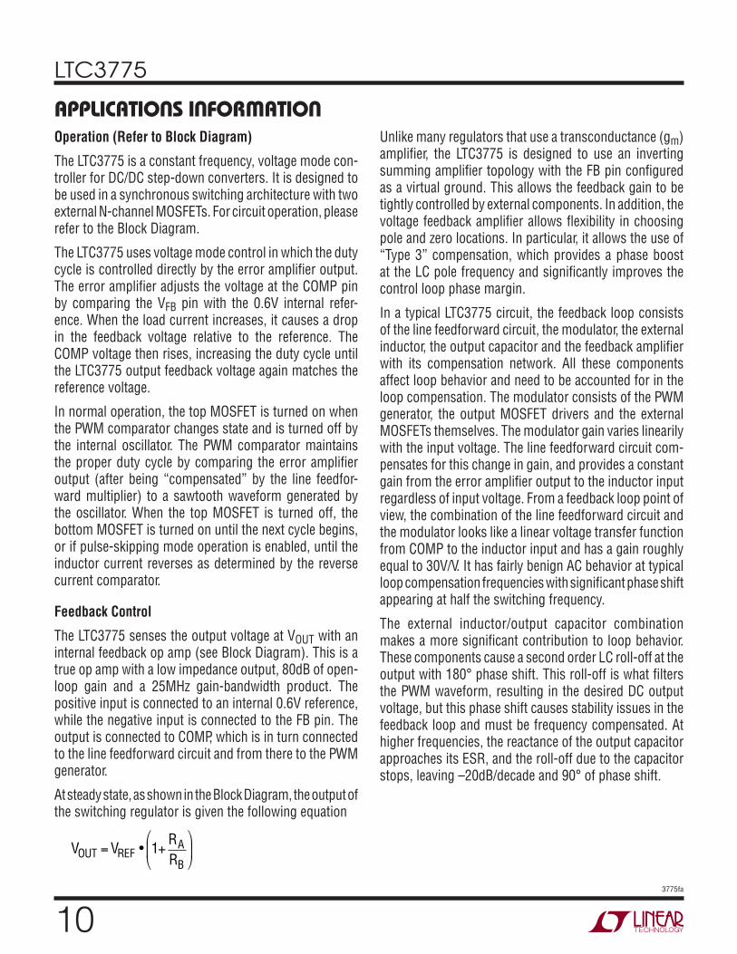
PIN FUNCTIONSILIMT (Pin 1/Pin 3): Topside Current Limit Set Point. This pin has an internal 100μA pull-down current, allowing the topside current limit threshold to be programmed by an external resistor connected to VIN. See Current Limit Applications.
ILIMB (Pin 2/Pin 4): Bottom Side Current Limit Set Point. This pin has an internal 10μA pull-up current, allowing the bottom side current limit threshold to be programmed by an external resistor connected to SGND. See Current Limit Applications.
FB (Pin 3/Pin 5): Error Amplifi er Input. The FB pin is connected to a resistive divider from VOUT to SGND. The feedback loop compensation network is also connected to this pin.
COMP (Pin 4/Pin 6): Error Amplifi er Output. Use an RC network between the COMP pin and the FB pin to compen-sate the feedback loop for optimum transient response.
SS (Pin 5/Pin 7): Soft-Start. Connect this pin to an external capacitor, CSS, to implement a soft-start function. When the voltage on the SS pin is less than the 0.6V internal reference, the LTC3775 regulates the VFB voltage to the SS pin voltage instead of the 0.6V reference.
FREQ (Pin 6/Pin 8): Frequency Set. A resistor connected from this pin to SGND sets the free-running frequency of the internal oscillator. See Applications Information section for resistor value selection details.
SGND (Pin 7/Pin 9): Signal Ground. All the internal low power circuitry returns to the SGND pin. All feedback and soft-start connections should return to SGND. SGND should be Kelvin connected to a single point near the negative terminal of the VOUT bypass capacitor.
BG (Pin 8/Pin 10): Bottom Gate Drive. This pin drives the gate of the bottom N-channel synchronous switch MOSFET. This pin swings from PGND to INTVCC.
INTVCC (Pin 9/Pin 11): Internal 5.2V Regulator Output. The gate driver and control circuits are powered from this voltage. Bypass this pin to power ground with a low ESR ce-ramic capacitor of value 4.7μF or greater (X5R or better).
SENSE (Pin 10/Pin 12): Topside Current Sensing Input. Connect this pin to the switch node of the converter for top MOSFET RDS(ON) current sensing. Alternatively, this
pin can be connected to a sense resistor at the drain of the top MOSFET for more accurate current limit.
VIN (Pin 11/Pin 13): Main Input Supply. Bypass this pin to PGND with a low ESR ceramic capacitor of value 1μF or greater (X5R or better).
SW (Pin 12/Pin 14): Switch Node. Connect this pin to the source of the upper power MOSFET. This pin is also used as the input to the bottom side current limit comparator and the zero-crossing reverse current comparator.
TG (Pin 13/Pin 15): Top Gate Drive. This pin drives the gate of the top N-channel MOSFET. The TG driver draws power from the BOOST pin and returns to the SW pin, providing true fl oating drive to the top MOSFET.
BOOST (Pin 14/Pin 16): Top Gate Driver Supply. This pin should be decoupled to SW with a 0.1μF low ESR ceramic capacitor. An external Schottky diode from INTVCC to BOOST creates a fl oating charge-pump supply at BOOST. No other external supplies are required.
MODE/SYNC (Pin 15/Pin 1): Pulse-Skipping Mode Enable/Sync Pin. This multifunction pin provides pulse-skipping mode enable/disable control and an external clock input for synchronization of the internal oscillator. Pulling this pin below 1.2V (DC) or driving it with an external logic-level syn-chronization signal disables pulse-skipping mode operation and forces continuous operation. Pulling the pin above 1.2V enables pulse-skipping mode operation. This pin has an internal 50k pull-down resistor connected to SGND.
RUN/SHDN (Pin 16/Pin 2): Enable/Shutdown Input. Pull-ing this pin above 1.22V enables the controller. Forcing this pin below 1.22V causes the driver outputs to pull low. Pulling this pin below 0.74V forces the LTC3775 into shutdown mode. While in shutdown, the INTVCC regulator and most internal circuitry turns off and the supply current drops below 14μA. This pin has an internal 1μA pull-up current that allows the LTC3775 to power up if this pin is left fl oating.
PGND (Exposed Pad Pin 17/Exposed Pad Pin 17): Power Ground. The BG driver returns to this pin. Connect PGND to the source of the bottom power MOSFET and the VIN and INTVCC bypass capacitors. PGND is electrically iso-lated from SGND. The exposed pad of the QFN and MSOP packages is connected to PGND.
(QFN/MSOP)
LTC3775
93775fa
BLOCK DIAGRAM
+
– PGND
TG
BOOST
ILIMB
VILIMB
VIN
RILIMB
RSENSE
SENSE
INTVCC
10μA
INTVCC
DB
L
CB
COUT
VOUT
3775 BD
QT
SW
IREV
MODE
0.6VEA
PWM
+
–
PGND
0.2 • VILIMB
CBLIM
+
–
CTLIM
+
SWITCHLOGIC ANDANTISHOOT-THROUGH
BGQB
PGND
FB
FB
C2
COMP
SGND
+
–
+
–
+
–
MAX
+
–
1μA
INTVCC
ISS
MODE
3.6V
UVLO
EN
0.6V
VIN
VIN
INTVCC
INTVCC
EXT SYNC
LINEFEEDFORWARD
MODE/SYNCDETECT
OVERTEMP
REF
5.2V REG
OSC
SS
0.66V
VIN
++–
CVCC
CSS
C1
C3
R3
R2
50k
RARB
SS
MODE/SYNC
FREQRSET
R5
R4
RUN/SHDN SHDN
VIN IRUN1μA
CHIPSHUTDOWN
1.22V
INTVCC
+
–
0.74V
RILIMTILIMT
INTVCC
100μA
LTC3775
103775fa
APPLICATIONS INFORMATIONOperation (Refer to Block Diagram)
The LTC3775 is a constant frequency, voltage mode con-troller for DC/DC step-down converters. It is designed to be used in a synchronous switching architecture with two external N-channel MOSFETs. For circuit operation, please refer to the Block Diagram.
The LTC3775 uses voltage mode control in which the duty cycle is controlled directly by the error amplifi er output. The error amplifi er adjusts the voltage at the COMP pin by comparing the VFB pin with the 0.6V internal refer-ence. When the load current increases, it causes a drop in the feedback voltage relative to the reference. The COMP voltage then rises, increasing the duty cycle until the LTC3775 output feedback voltage again matches the reference voltage.
In normal operation, the top MOSFET is turned on when the PWM comparator changes state and is turned off by the internal oscillator. The PWM comparator maintains the proper duty cycle by comparing the error amplifi er output (after being “compensated” by the line feedfor-ward multiplier) to a sawtooth waveform generated by the oscillator. When the top MOSFET is turned off, the bottom MOSFET is turned on until the next cycle begins, or if pulse-skipping mode operation is enabled, until the inductor current reverses as determined by the reverse current comparator.
Feedback Control
The LTC3775 senses the output voltage at VOUT with an internal feedback op amp (see Block Diagram). This is a true op amp with a low impedance output, 80dB of open-loop gain and a 25MHz gain-bandwidth product. The positive input is connected to an internal 0.6V reference, while the negative input is connected to the FB pin. The output is connected to COMP, which is in turn connected to the line feedforward circuit and from there to the PWM generator.
At steady state, as shown in the Block Diagram, the output of the switching regulator is given the following equation
VOUT =VREF • 1+RARB
Unlike many regulators that use a transconductance (gm) amplifi er, the LTC3775 is designed to use an inverting summing amplifi er topology with the FB pin confi gured as a virtual ground. This allows the feedback gain to be tightly controlled by external components. In addition, the voltage feedback amplifi er allows fl exibility in choosing pole and zero locations. In particular, it allows the use of “Type 3” compensation, which provides a phase boost at the LC pole frequency and signifi cantly improves the control loop phase margin.
In a typical LTC3775 circuit, the feedback loop consists of the line feedforward circuit, the modulator, the external inductor, the output capacitor and the feedback amplifi er with its compensation network. All these components affect loop behavior and need to be accounted for in the loop compensation. The modulator consists of the PWM generator, the output MOSFET drivers and the external MOSFETs themselves. The modulator gain varies linearily with the input voltage. The line feedforward circuit com-pensates for this change in gain, and provides a constant gain from the error amplifi er output to the inductor input regardless of input voltage. From a feedback loop point of view, the combination of the line feedforward circuit and the modulator looks like a linear voltage transfer function from COMP to the inductor input and has a gain roughly equal to 30V/V. It has fairly benign AC behavior at typical loop compensation frequencies with signifi cant phase shift appearing at half the switching frequency.
The external inductor/output capacitor combination makes a more signifi cant contribution to loop behavior. These components cause a second order LC roll-off at the output with 180° phase shift. This roll-off is what fi lters the PWM waveform, resulting in the desired DC output voltage, but this phase shift causes stability issues in the feedback loop and must be frequency compensated. At higher frequencies, the reactance of the output capacitor approaches its ESR, and the roll-off due to the capacitor stops, leaving –20dB/decade and 90° of phase shift.

LTC3775
113775fa
APPLICATIONS INFORMATIONFigure 1 shows a Type 3 amplifi er. The transfer function of this amplifi er is given by the following equation:
VCOMPVOUT
=– 1+ sR2C1( ) 1+ s(RA +R3)C3
sRA C1+C2( ) 1+ s(C1||C2)R2( ) 1+ sC3R3( )
The RC network across the error amplifi er and the feed-forward components R3 and C3 introduce two pole-zero pairs to obtain a phase boost at the system unity-gain frequency, fC. In theory, the zeros and poles are placed symmetrically around fC, and the spread between the zeros and the poles is adjusted to give the desired phase boost at fC. However, in practice, if the crossover frequency is much higher than the LC double-pole frequency, this method of frequency compensation normally generates a phase dip within the unity bandwidth and creates some concern regarding conditional stability.
If conditional stability is a concern, move the error ampli-fi er’s zero to a lower frequency to avoid excessive phase dip. The following equations can be used to compute the feedback compensation component values:
f switching frequency
fLC
fR
SW
LCOUT
ESR
=
=π
=π
1
2
1
2 EESR OUTC
choose:
f crossover frequencyf
f f
CSW
Z ERR LC
= =
= =π
10
1
21( ) RR C
ff
R R C
f f
Z RESC
A
P ERR ESR
2 1
5
1
2 3 32
1
( )
( )
= =π +( )
= ==π
= =π
1
2 2 1 2
51
2 3 32
R C C
f fR CP RES C
( || )
( )
Required error amplifi er gain at frequency fC:
AV(CROSSOVER)
40log 1+fCfLC
2
– 20log 1+fCfESR
2
– 20log AMOD( )
20log R2RA
•
1+fLCfC
1+fP2(RES)
fC+fP2(RES) – fZ2(RES)
fZ2(RES)
1+fCfESR
+fLC
fESR – fLC1+
fP2(RES)fC
where AMOD is the modulator and line feedforward gain and is equal to:
A
V DC
V
V
VV VMOD
IN MAX MAX
SAW
≈ = ≈( ) • • .
./
40 0 95
1 2530
Once the value of resistor RA and the pole and zero loca-tions have been decided, the values of C1, R2, C2, R3 and C3 can be obtained from the above equations.
Compensating a switching power supply feedback loop is a complex task. The applications shown in this data sheet show typical values, optimized for the power components shown. Though similar power components should suffi ce, substantially changing even one major power component may degrade performance signifi cantly. Stability also may depend on circuit board layout. To verify the calculated component values, all new circuit designs should be prototyped and tested for stability.
–
+
VOUT
VREF
RA R3
C3R2
C1
GA
IN (
dB
)
C2
FBRB COMP
FREQ
–1
–1+1GAIN
PHASE
BOOST
0
PH
AS
E (D
EG
)
–90
–180
–270
–3803775 F01
Figure 1. Type 3 Amplifi er Compensation

LTC3775
123775fa
APPLICATIONS INFORMATIONOutput Overvoltage Protection
An overvoltage comparator, MAX, guards against transient overshoots (>10%) as well as other more serious condi-tions that may overvoltage the output. In such cases, the top MOSFET is turned off and the bottom MOSFET is turned on until the overvoltage condition is cleared.
Run/Shutdown
The LTC3775 can be put into a low power shutdown mode with quiescent current <14μA by pulling the RUN/SHDN pin below 0.74V. The RUN/SHDN pin can also be used as an accurate external UVLO (undervoltage lockout) input with a threshold of 1.22V. The driver outputs stay low if this pin is <1.22V. The external resistive divider R4 and R5 shown in the Block Diagram can be used to set the UVLO level based on VIN. The VIN voltage at which the switching starts is given by the following formula:
UVLO (Upper) = 1.22V • (1 + R4/R5) – (1μA • R4)
The RUN/SHDN pin has an internal 1μA pull-up for default turn-on if this pin is left fl oating. This 1μA pull-up current is included in the above UVLO calculation. When RUN/SHDN goes above 1.22V, this pull-up current is increased to 5μA. This provides some amount of hysteresis to the UVLO threshold. The lower UVLO level becomes:
UVLO (Lower) = 1.22V • (1 + R4/R5) – (5μA • R4)
So the amount of hysteresis is given by:
UVLO (Hysteresis) = 4μA • R4
Soft-Start
The LTC3775 includes a soft-start circuit that provides a smooth output voltage ramp during start-up. The SS pin requires an external capacitor, CSS, to GND with the value determined by the required soft-start time. An internal 1μA current source charges CSS. When the voltage on the SS pin is less than the 0.6V internal reference, the LTC3775 regulates the VFB voltage to the SS pin voltage instead of the 0.6V reference. As the SS voltage rises linearly from 0V to 0.6V and beyond, the output voltage, VOUT , rises smoothly from zero to its fi nal value. The total soft-start time can be calculated as:
t
CμASOFTSTART
SS=0 9
1. •
The SS pin is pulled low in the following conditions: during an LDO undervoltage condition (INTVCC < 3.6V), during shutdown (RUN pin < 1.22V), during an overtemperature condition (TJ > 165°C) and during current limit.
If either the top or bottom current limit comparator trips, the SS pin is pulled low until the inductor current regu-lates at around the current limit setting. Once the fault is cleared, SS will start charging up allowing the duty cycle and output voltage to increase gradually. Due to the cur-rent limit action on the SS pin, it is important to avoid an overcurrent condition during start-up of the power supply, or VOUT will fail to start up properly.
0.74V+
–
+
–
1.22VTURN OFF TG
EN
4μA
RUN
R4R5
3775 F02
IRUN1μA
VIN
SHDN
LTC3775
CHIPSHUTDOWN
Figure 2. RUN Pin Control
Figure 3. Typical Start-Up Waveform for a Buck Converter Using the LTC3775
IL5A/DIV
VOUT0.5V/DIV
VSS1V/DIV
2ms/DIV 3775 F03VIN = 12VVOUT = 1.2VCSS = 0.01μFMODE = 0VSW FREQ = 500kHz
SWITCHOVERFROM PULSE-SKIPPING TO CONTINUOUSMODE

LTC3775
133775fa
APPLICATIONS INFORMATIONTo prevent discharging a pre-biased VOUT, the LTC3775 always starts switching in pulse-skipping mode up to SS = 0.54V, regardless of the mode selected by the MODE/SYNC pin. Thus if VOUT > 0V during power-up, VOUT will remain at the pre-biased voltage (if there is no load) until the SS voltage catches up with VOUT, after which VOUT will track the SS ramp. The LTC3775 reverts to the selected mode once SS > 0.54V.
Constant Switching Frequency
The internal oscillator can be programmed from 250kHz to 1MHz with an external resistor from the FREQ pin to ground, in order to optimize component size, effi ciency and noise for the specifi c application. The internal oscillator can also be synchronized to an external clock connected to the MODE/SYNC pin and can lock to a range of ±20% of the programmed free-running frequency. When locked to an external clock, pulse-skipping mode operation is automatically disabled. Constant frequency operation of-fers a number of benefi ts: inductor and capacitor values can be chosen for a precise operating frequency and the feedback loop can be similarly tightly specifi ed. Noise generated by the circuit will always be at known frequen-cies. Subharmonic oscillation and slope compensation, common headaches with constant frequency current mode switchers, are absent in voltage mode designs like the LTC3775.
Thermal Shutdown
The LTC3775 has a thermal detector that pulls the driver outputs low if the junction temperature of the chip ex-ceeds 165°C. The thermal shutdown circuit has 25°C of hysteresis.
Current Limit
The LTC3775 includes an onboard cycle-by-cycle current limit circuit that limits the maximum output current to a user-programmed level. The current limit circuit consists of two comparators, CTLIM and CBLIM that monitor the voltage drop across the top and bottom MOSFETs respec-tively. Since the MOSFET ’s effective resistance, RDS(ON),
is low during its on-time, the voltage drop from the drain to source is proportional to the current fl ow. Alternatively, for better accuracy, the topside current may be monitored with a sense resistor.
The benefi t of having two comparators is to allow continu-ous monitoring and cycle-by-cycle control of the inductor current regardless of the operating duty cycle. In high duty cycle operation the top MOSFET, QT , is on most of the time. Thus, a high side comparator is necessary to limit the output current during high duty cycle operation. Architectures that contain only one comparator to monitor the low side MOSFET will not effectively limit the output current during high duty cycle operation. Conversely, during low duty cycle operation, a low side comparator is neces-sary to limit the output current. Another common current sensing scheme uses a sense resistor in series with the inductor to allow continuous monitoring. However, this scheme restricts the range of VOUT due to the common mode range of the current limit comparator. The LTC3775 does not have this VOUT restriction.
Figure 4 shows the current limit circuitry. The top current limit comparator, CTLIM monitors the current through the top MOSFET, QT , when TG is high. If the inductor current exceeds the current limit threshold when QT is on, QT turns off immediately and the bottom MOSFET, QB, turns on. The SENSE pin is the input for CTLIM. For applications where
Figure 4. LTC3775 Current Limit Circuit
+
+
– 100μA
RILIMB
(OPT)10μA
0.2 • VILIMB
RILIMT
VINLTC3775
RSENSE
SENSE
CTLIM
TURN OFF TG
+
–CBLIM
EXTEND BG
ILIMB
SW
ILIMT
TG QT
VIN
BG QB
VOUT
3775 F04
PGND
SGND

LTC3775
143775fa
APPLICATIONS INFORMATIONthe upper MOSFET ’s RDS(ON) is used to sense current, connect the SENSE pin to the source of QT (the SW node). Alternatively, for accurate current sensing, connect this pin to a sense resistor located at the drain of QT . The reference input of CTLIM is connected to the ILIMT pin. Connect an external resistor, RILIMT , from the ILIMT pin to VIN to set the the current limit threshold. The voltage at the SENSE pin drops as the inductor current increases. CTLIM trips if the voltage at the SENSE pin goes below the voltage at the ILIMT pin causing TG to pull low and turn off QT .
The bottom current limit comparator, CBLIM, monitors the current through the bottom MOSFET, QB, when BG is high. If the inductor current exceeds the current limit threshold when QB is on, QB remains on until the current drops below the threshold. The SW pin is the input for CBLIM. The reference input to CBLIM is derived from the voltage at the ILIMB pin. Connect an external resistor, RILIMB, from the ILIMB pin to SGND to set the current limit threshold.
The inductor current fl ows from PGND to SW when QB is on (for a positive load current). The SW node is therefore a negative voltage. The LTC3775 inverts the voltage at the SW pin before comparing it with the attenuated voltage (5×) at the ILIMB pin. BG stays high once CBLIM trips and TG remains low until the inductor current drops below the threshold. Figure 5 shows typical waveforms during output overload.
Current Limit Blanking Time
The LTC3775 current limit circuit features a short blanking time following low-to-high and high-to-low transitions at the SW node. This prevents false tripping of the current limit circuit if there is ringing on the SW node.
When the top gate, TG, goes high, the topside comparator, CTLIM, waits for 200ns before turning on to monitor the SENSE voltage. Likewise, when the bottom gate, BG, goes high the bottom side comparator, CBLIM, waits for 200ns before turning on to monitor the SW voltage. This means that the minimum TG and BG pulse is slightly more than 200ns during current limit. These blanking times do not, however, limit the duty cycle capability of the control loop. The LTC3775 control loop is capable of operation with a TG on-time as low as 30ns.
If a sense resistor is employed on the top side, the LTC3775 automatically lowers the CTLIM blanking time from 200ns to 100ns. The CBLIM blanking time remains at 200ns. The blanking time can be reduced when a sense resistor is used because the SENSE pin connects to the drain of the top MOSFET which rings less than the SW node. The LTC3775 detects that a sense resistor is employed by checking that the SENSE pin stays high (equal to VIN) when BG is high. If the SENSE pin is connected to the SW node, SENSE will be at 0V when BG is high.
The Current Sensing Input Pins
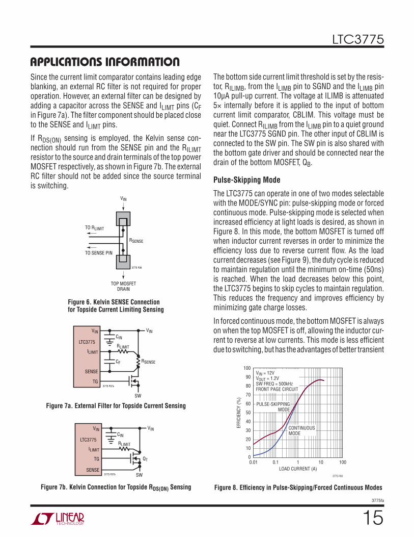
The SENSE and ILIMT pins are inputs to the top current limit comparator, CTLIM. The top current limit threshold is set by the resistor, RILIMT , connected to the ILIMT pin and the ILIMT pin 100μA pull-down current. RILIMT should be placed close to the LTC3775 and the other end of RILIMT should run parallel with the SENSE trace to the Kelvin sense connection underneath the sense resistor, as shown in Figure 6. The sense resistor should be connected to the drain of the top power MOSFET and the VIN node using short, wide PCB traces. Ideally, the top terminal of the sense resistors will be immediately adjacent to the posi-tive terminal of the input capacitor, as shown in Figure 7a. This path is a part of the high di/dt loop formed by the sense resistor, top power MOSFET, inductor and output capacitor.
Figure 5. Typical Waveforms During Output Overload
VSS1V/DIV
IL20A/DIV
20μs/DIV 3775 F05VIN = 12VVOUT = 1.2VCSS = 0.01μFFIRST PAGE CIRCUIT
0A LOAD
LTC3775
153775fa
Figure 8. Effi ciency in Pulse-Skipping/Forced Continuous Modes
Since the current limit comparator contains leading edge blanking, an external RC fi lter is not required for proper operation. However, an external fi lter can be designed by adding a capacitor across the SENSE and ILIMT pins (CF in Figure 7a). The fi lter component should be placed close to the SENSE and ILIMT pins.
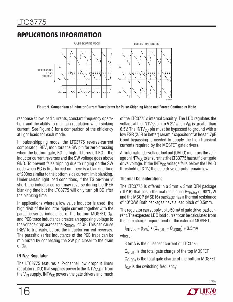
If RDS(ON) sensing is employed, the Kelvin sense con-nection should run from the SENSE pin and the RILIMT resistor to the source and drain terminals of the top power MOSFET respectively, as shown in Figure 7b. The external RC fi lter should not be added since the source terminal is switching.
The bottom side current limit threshold is set by the resis-tor, RILIMB, from the ILIMB pin to SGND and the ILIMB pin 10μA pull-up current. The voltage at ILIMB is attenuated 5× internally before it is applied to the input of bottom current limit comparator, CBLIM. This voltage must be quiet. Connect RILIMB from the ILIMB pin to a quiet ground near the LTC3775 SGND pin. The other input of CBLIM is connected to the SW pin. The SW pin is also shared with the bottom gate driver and should be connected near the drain of the bottom MOSFET, QB.
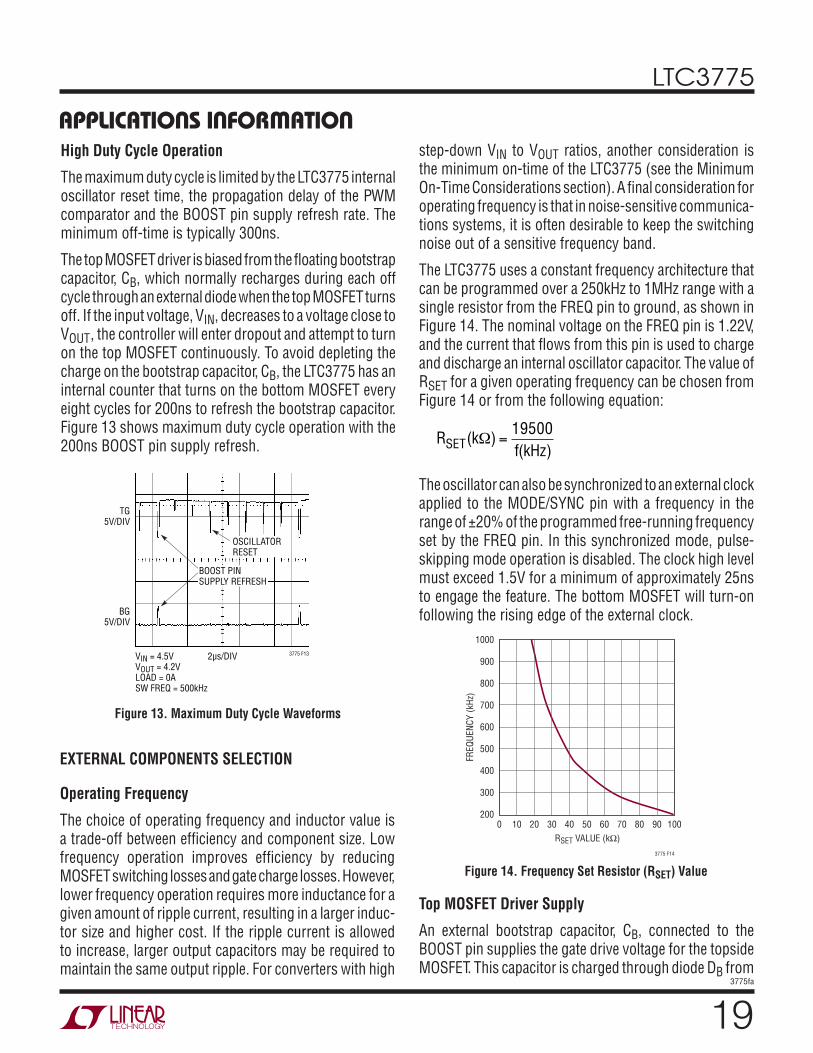
Pulse-Skipping Mode
The LTC3775 can operate in one of two modes selectable with the MODE/SYNC pin: pulse-skipping mode or forced continuous mode. Pulse-skipping mode is selected when increased effi ciency at light loads is desired, as shown in Figure 8. In this mode, the bottom MOSFET is turned off when inductor current reverses in order to minimize the effi ciency loss due to reverse current fl ow. As the load current decreases (see Figure 9), the duty cycle is reduced to maintain regulation until the minimum on-time (50ns) is reached. When the load decreases below this point, the LTC3775 begins to skip cycles to maintain regulation. This reduces the frequency and improves effi ciency by minimizing gate charge losses.
In forced continuous mode, the bottom MOSFET is always on when the top MOSFET is off, allowing the inductor cur-rent to reverse at low currents. This mode is less effi cient due to switching, but has the advantages of better transient
APPLICATIONS INFORMATION
RSENSE
3775 F06
TO RLIMIT
TO SENSE PIN
VIN
TOP MOSFETDRAIN
VIN
CIN
CF
RLIMIT
RSENSE
3775 F07a
VIN
LTC3775
ILIMIT
SENSE
TG
SW
Figure 6. Kelvin SENSE Connection for Topside Current Limiting Sensing
Figure 7a. External Filter for Topside Current Sensing
VIN
CIN
RLIMIT
QT
3775 F07b
VIN
LTC3775
ILIMIT
SENSE
TG
SW
Figure 7b. Kelvin Connection for Topside RDS(ON) Sensing
LOAD CURRENT (A)
30
EFF
ICIE
NC
Y (
%)
90
100
20
10
80
50
70
60
40
0.01 1 10 100
3775 F08
00.1
VIN = 12VVOUT = 1.2VSW FREQ = 500kHzFRONT PAGE CIRCUIT
PULSE-SKIPPINGMODE
CONTINUOUSMODE
LTC3775
163775fa
response at low load currents, constant frequency opera-tion, and the ability to maintain regulation when sinking current. See Figure 8 for a comparison of the effi ciency at light loads for each mode.
In pulse-skipping mode, the LTC3775 reverse-current comparator, IREV , monitors the SW pin for zero crossing when the bottom gate, BG, is high. It turns off BG if the inductor current reverses and the SW voltage goes above GND. To prevent false tripping due to ringing on the SW node when BG is fi rst turned on, there is a blanking time of 200ns similar to the bottom side current limit blanking. Under certain light load conditions, if the TG on-time is short, the inductor current may reverse during the IREV blanking time but the LTC3775 will only turn off BG after the blanking time.
In applications where a low value inductor is used, the high di/dt of the inductor ripple current together with the parasitic series inductance of the bottom MOSFET, QB, and PCB trace inductance creates an opposing voltage to the voltage drop across the RDS(ON) of QB. This can cause IREV to trip early, before the inductor current reverses. The parasitic series inductance of the PCB trace can be minimized by connecting the SW pin closer to the drain of QB.
INTVCC Regulator
The LTC3775 features a P-channel low dropout linear regulator (LDO) that supplies power to the INTVCC pin from the VIN supply. INTVCC powers the gate drivers and much
of the LTC3775’s internal circuitry. The LDO regulates the voltage at the INTVCC pin to 5.2V when VIN is greater than 6.5V. The INTVCC pin must be bypassed to ground with a low ESR (X5R or better) ceramic capacitor of at least 4.7μF. Good bypassing is needed to supply the high transient currents required by the MOSFET gate drivers.
An internal undervoltage lockout (UVLO) monitors the volt-age on INTVCC to ensure that the LTC3775 has suffi cient gate drive voltage. If the INTVCC voltage falls below the UVLO threshold of 3.1V, the gate drive outputs remain low.
Thermal Considerations
The LTC3775 is offered in a 3mm × 3mm QFN package (UD16) that has a thermal resistance RTH(JA) of 68°C/W and the MSOP (MSE16) package has a thermal resistance of 40°C/W. Both packages have a lead pitch of 0.5mm.
The regulator can supply up to 50mA of gate drive load cur-rent. The expected LDO load current can be calculated from the gate charge requirement of the external MOSFET:
IINTVCC = (fSW) • (QG(QT) + QG(QB)) + 3.5mA
where:
3.5mA is the quiescent current of LTC3775
QG(QT) is the total gate charge of the top MOSFET
QG(QB) is the total gate charge of the bottom MOSFET
fSW is the switching frequency
APPLICATIONS INFORMATION
Figure 9. Comparison of Inductor Current Waveforms for Pulse-Skipping Mode and Forced Continuous Mode
PULSE-SKIPPING MODE FORCED CONTINUOUS
DECREASINGLOAD
CURRENT
0A
0A
0A
0A
0A
0A
3775 F09

LTC3775
173775fa
The value of QG should come from the plot of VGS vs QG in the Typical Performance Characteristics section of the MOSFET data sheet. The value listed in the electrical specifi cations may be measured at a higher VGS, such as 10V, whereas the value of interest is at the 5V INTVCC gate drive voltage.
Care must be taken to ensure that the maximum junction temperature of the LTC3775 is never exceeded. The junc-tion temperature can be estimated using the following equations:
PDISS = VIN • IINTVCC
TJ = TA + PDISS • RTH(JA)
As an example of the required thermal analysis, consider a buck converter with a 24V input voltage and an output voltage of 3.3V at 15A. The switching frequency is 500kHz and the maximum ambient temperature is 70°C. The power MOSFET used for this application is the Vishay Siliconix Si7884DP, which has a typical RDS(ON) of 7.5mΩ at VGS = 4.5V and 5.5mΩ at VGS = 10V. From the plot of VGS vs QG, the total gate charge at VGS = 5V is 18.5nC (the tem-perature coeffi cient of the gate charge is low). One power MOSFET is used for the top side and one for the bottom side. For the UD package:
IINTVCC = 3.5mA + 2 • 18.5nC • 500kHz = 22mA
PDISS = 24V • 22mA = 528mW
TJ = 70°C + 528mW • 68°C/W = 105.9°C
In this example, the junction temperature rise is 35.9°C. These equations demonstrate how the gate charge cur-rent typically dominates the quiescent current of the IC, and how the choice of the operating frequency and board heat sinking can have a signifi cant effect on the thermal performance of the solution.
To prevent the maximum junction temperature from be-ing exceeded, the input supply current of the IC should be checked when operating in continuous mode (heavy load) at maximum VIN. A trade-off between the operat-ing frequency and the size of the power MOSFETs may need to be made in order to maintain a reliable junction temperature.
Finally, it is important to verify the calculations by perform-ing a thermal analysis of the fi nal PCB using an infrared camera or thermal probe.
Operation at Low Supply Voltage
The LTC3775 has a minimum input voltage of 4.5V. The gate driver for the LTC3775 consists of a PMOS pull-up and an NMOS pull-down device, allowing the full INTVCC voltage to be applied to the gates during power MOSFET switching. Nonetheless, care should be taken to deter-mine the minimum gate drive supply voltage (INTVCC) in order to choose the optimum power MOSFETs. Important parameters that can affect the minimum gate drive volt-age are the minimum input voltage (VIN(MIN)), the LDO dropout voltage, the QG of the power MOSFETs, and the operating frequency.
If the input voltage VIN is low enough for the INTVCC LDO to be in dropout, then the minimum gate drive supply voltage is:
VINTVCC = VIN(MIN) – VDROPOUT
The LDO dropout voltage is a function of the total gate drive current and the quiescent current of the IC (typically 3.5mA). A curve of dropout voltage versus output cur-rent for the LDO is shown in Figure 10. The temperature coeffi cient of the LDO dropout voltage is approximately 6000ppm/°C. See the INTVCC Regulator and Thermal Considerations sections for information about calculating the total quiescent current.
APPLICATIONS INFORMATION
Figure 10. INTVCC LDO Dropout Voltage vs Current
INTVCC LOAD CURRENT (mA)
0
INTV
CC D
RO
PO
UT V
OLT
AG
E (
V)
–0.4
–0.2
0
40
3775 F10
–0.6
–0.8
–1.010 20 30 50
TA = 25°C

LTC3775
183775fa
After the calculations have been completed, it is impor-tant to measure the gate drive waveforms and the gate driver supply voltage (INTVCC to PGND) over all operating conditions (low VIN, nominal VIN and high VIN, as well as from light load to full load) to ensure adequate power MOSFET enhancement. Consult the power MOSFET data sheet to determine the actual RDS(ON) for the measured VGS, and verify your thermal calculations by measuring the component temperatures using an infrared camera or thermal probe.
Operation at High Supply Voltage
At high input voltages, the LTC3775’s internal LDO can dissipate a signifi cant amount of power, which could cause the maximum junction temperature to be exceeded. Conditions such as a high operating frequency, or the use of more than one power MOSFET in parallel, could push the junction temperature rise to high levels. To prevent the maximum junction temperature from being exceeded, the input supply current must be checked while operating in continuous conduction mode at maximum VIN. See the Thermal Considerations section for calculation of the maximum junction temperature.
Low Duty Cycle Operation
The LTC3775 uses a leading edge modulation architec-ture. Because the top MOSFET turns on when the PWM comparator trips, the top MOSFET minimum on-time is not dependent on the propagation delay of the PWM comparator; it is only limited by the internal delays of the gate drivers and the rise/fall time of the power MOSFET gate. This allows the LTC3775 to operate in very low duty cycle applications with a large step-down ratio. Figure 11 shows minimum on-time waveforms for forced continuous mode operation.
If pulse-skipping mode is selected, the LTC3775 allows the controller to skip pulses at light load, thereby reducing switching losses and improving the effi ciency. Figure 12 shows waveforms of the minimum on-time in pulse-skip-ping mode.
If the TG on-time is less than the blanking time of the topside current limit comparator, CTLIM, the topside comparator never trips during normal operation. The blanking time
is 200ns for RDS(ON) sensing and 100ns when a sense resistor is used. For TG on-times smaller than the topside blanking times, the LTC3775 relies on the bottom current limit comparator, CBLIM, to monitor the inductor current. If CBLIM trips, the LTC3775 starts to skip pulses and at the same time pulls down the soft-start capacitor to limit the duty cycle. If VOUT drops suffi ciently, the TG on-time can increase enough to turn on CTLIM and limit the peak inductor current. The minimum on-time of the application circuit can be calculated at maximum VIN:
tV
f VON MINOUT
SW IN MAX( )
( )•=
APPLICATIONS INFORMATION
Figure 11. Minimum On-Time Waveforms in Forced Continuous Mode
Figure 12. Minimum On-Time Waveforms in Pulse-Skipping Mode
VSW10V/DIV
TG10V/DIV
20ns/DIV 3775 F11VIN = 28VVOUT = 0.6VLOAD = 1AMODE/SYNC = 0VSW FREQ = 1MHz
VSW10V/DIV
TG10V/DIV
20ns/DIV 3775 F12VIN = 28VVOUT = 0.6VLOAD = 1AMODE/SYNC = INTVCCSW FREQ = 1MHz
LTC3775
193775fa
High Duty Cycle Operation
The maximum duty cycle is limited by the LTC3775 internal oscillator reset time, the propagation delay of the PWM comparator and the BOOST pin supply refresh rate. The minimum off-time is typically 300ns.
The top MOSFET driver is biased from the fl oating bootstrap capacitor, CB, which normally recharges during each off cycle through an external diode when the top MOSFET turns off. If the input voltage, VIN, decreases to a voltage close to VOUT , the controller will enter dropout and attempt to turn on the top MOSFET continuously. To avoid depleting the charge on the bootstrap capacitor, CB, the LTC3775 has an internal counter that turns on the bottom MOSFET every eight cycles for 200ns to refresh the bootstrap capacitor. Figure 13 shows maximum duty cycle operation with the 200ns BOOST pin supply refresh.
step-down VIN to VOUT ratios, another consideration is the minimum on-time of the LTC3775 (see the Minimum On-Time Considerations section). A fi nal consideration for operating frequency is that in noise-sensitive communica-tions systems, it is often desirable to keep the switching noise out of a sensitive frequency band.
The LTC3775 uses a constant frequency architecture that can be programmed over a 250kHz to 1MHz range with a single resistor from the FREQ pin to ground, as shown in Figure 14. The nominal voltage on the FREQ pin is 1.22V, and the current that fl ows from this pin is used to charge and discharge an internal oscillator capacitor. The value of RSET for a given operating frequency can be chosen from Figure 14 or from the following equation:
RSET(k ) = 19500f(kHz)
The oscillator can also be synchronized to an external clock applied to the MODE/SYNC pin with a frequency in the range of ±20% of the programmed free-running frequency set by the FREQ pin. In this synchronized mode, pulse-skipping mode operation is disabled. The clock high level must exceed 1.5V for a minimum of approximately 25ns to engage the feature. The bottom MOSFET will turn-on following the rising edge of the external clock.
APPLICATIONS INFORMATION
Figure 13. Maximum Duty Cycle Waveforms
RSET VALUE (kΩ)
0
FREQ
UEN
CY
(kH
z)
1000
900
800
700
600
500
400
300
20080
3775 F14
20 40 60 1007010 30 50 90
Figure 14. Frequency Set Resistor (RSET) Value
BG5V/DIV
TG5V/DIV
2μs/DIV 3775 F13VIN = 4.5VVOUT = 4.2VLOAD = 0ASW FREQ = 500kHz
OSCILLATORRESET
BOOST PINSUPPLY REFRESH
EXTERNAL COMPONENTS SELECTION
Operating Frequency
The choice of operating frequency and inductor value is a trade-off between effi ciency and component size. Low frequency operation improves effi ciency by reducing MOSFET switching losses and gate charge losses. However, lower frequency operation requires more inductance for a given amount of ripple current, resulting in a larger induc-tor size and higher cost. If the ripple current is allowed to increase, larger output capacitors may be required to maintain the same output ripple. For converters with high
Top MOSFET Driver Supply
An external bootstrap capacitor, CB, connected to the BOOST pin supplies the gate drive voltage for the topside MOSFET. This capacitor is charged through diode DB from
LTC3775
203775fa
INTVCC when the switch node is low. When the top MOSFET turns on, the switch node rises to VIN and the BOOST pin rises to approximately VIN + INTVCC. The boost capacitor needs to store at least 100 times the gate charge required by the top MOSFET. In most applications a 0.1μF to 1μF X5R or X7R dielectric capacitor is adequate. The reverse breakdown of the Schottky diode, DB, must be greater than VIN(MAX).
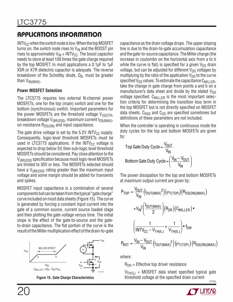
Power MOSFET Selection
The LTC3775 requires two external N-channel power MOSFETs, one for the top (main) switch and one for the bottom (synchronous) switch. Important parameters for the power MOSFETs are the threshold voltage V(GS)TH, breakdown voltage V(BR)DSS, maximum current IDS(MAX), on-resistance RDS(ON) and input capacitance.
The gate drive voltage is set by the 5.2V INTVCC supply. Consequently, logic-level threshold MOSFETs must be used in LTC3775 applications. If the INTVCC voltage is expected to drop below 5V, then sub-logic level threshold MOSFETs should be considered. Pay close attention to the V(BR)DSS specifi cation because most logic-level MOSFETs are limited to 30V or less. The MOSFETs selected should have a V(BR)DSS rating greater than the maximum input voltage and some margin should be added for transients and spikes.
MOSFET input capacitance is a combination of several components but can be taken from the typical “gate charge” curve included on most data sheets (Figure 15). The curve is generated by forcing a constant input current into the gate of a common source, current source loaded stage and then plotting the gate voltage versus time. The initial slope is the effect of the gate-to-source and the gate-to-drain capacitance. The fl at portion of the curve is the result of the Miller multiplication effect of the drain-to-gate
capacitance as the drain voltage drops. The upper sloping line is due to the drain-to-gate accumulation capacitance and the gate-to-source capacitance. The Miller charge (the increase in coulombs on the horizontal axis from a to b while the curve is fl at) is specifi ed for a given VDS drain voltage, but can be adjusted for different VDS voltages by multiplying by the ratio of the application VDS to the curve specifi ed VDS values. To estimate the capacitance CMILLER, take the change in gate charge from points a and b on a manufacturer’s data sheet and divide by the stated VDS voltage specifi ed. CMILLER is the most important selec-tion criteria for determining the transition loss term in the top MOSFET but is not directly specifi ed on MOSFET data sheets. CRSS and COS are specifi ed sometimes but defi nitions of these parameters are not included.
When the controller is operating in continuous mode the duty cycles for the top and bottom MOSFETs are given by:
Top Gate Duty Cycle=VOUTVIN
Bottom Gate Duty Cycle=VIN – VOUT
VIN
The power dissipation for the top and bottom MOSFETs at maximum output current are given by:
PTOP =VOUT
VIN
IOUT MAX)2( )( T(TOP)( ) RDS(ON)(MAX)( )
+VIN2
IOUT(MAX)
2RDR( ) CMILLER( ) •
1
INTVCC – VTH(IL)
+1
VTH(IL)
• fSW
PBOT =VIN – VOUT
VIN
IOUT( AX)2( )M T(TOP)( ) RDS(ON)(MAX)( )
where:
RDR = Effective top driver resistance
VTH(IL) = MOSFET data sheet specifi ed typical gate threshold voltage at the specifi ed drain current
APPLICATIONS INFORMATION
+
–VDS
VIN
VGS
MILLER EFFECT
QIN
a b
CMILLER = (QB – QA)/VDS
VGSV
+
–3775 F15
Figure 15. Gate Charge Characteristics
LTC3775
213775fa
CMILLER = Calculated Miller capacitance using the gate charge curve from the MOSFET data sheet
fSW = Switching frequency
Both MOSFETs have conduction losses (I2R) while the topside N-channel equation includes an additional term for transition losses, which peak at the highest input volt-age. For VIN < 12V, the high current effi ciency generally improves with larger MOSFETs, while for VIN > 12V, the transition losses rapidly increase to the point that the use of a higher RDS(ON) device with lower CMILLER actually provides higher effi ciency. The bottom MOSFET losses are greatest at high input voltage when the top switch duty factor is low or during a short circuit when the bottom switch is on close to 100% of the period.
Schottky Diode Selection
An optional Schottky diode connected between the SW node (cathode) and the source of the bottom MOSFET (anode) conducts during the dead time between the conduction of the power MOSFET switches. It is intended to prevent the body diode of the bottom MOSFET from turning on and storing a charge during the dead time, which can cause a modest (about 1%) effi ciency loss. The diode can be rated for about one half to one fi fth of the full load current since it is on for only a fraction of the duty cycle. In order for the diode to be effective, the inductance between it and the bottom MOSFET must be as small as possible, mandating that these components be placed next to each other on the same layer of the PC board.
Input Capacitor Selection
The input bypass capacitor has three primary requirements: its ESR must be low to minimize the supply drop when the top MOSFETs turn on, its RMS current capability must be adequate to withstand the ripple current at the input, and its capacitance must be large enough to maintain the input voltage until the input supply can respond. Generally, a capacitor (particularly a non-ceramic type) that meets the fi rst two parameters will have far more capacitance than is required to keep capacitance-based droop under control. The input capacitor’s voltage rating should be at least 1.4 times the maximum input voltage.
In continuous mode, the source current of the top N-channel MOSFET is approximately a square wave of duty cycle VOUT/VIN. The maximum RMS capacitor current is given by:
I I
V V V
VRMS OUT MAXOUT IN OUT
IN≈
( )( )
–
This formula has a maximum at VIN = 2VOUT , where IRMS = IOUT/2. This simple worst-case condition is com-monly used for design because even signifi cant deviations do not offer much relief.
Note that capacitor manufacturer’s ripple current ratings are often based on only 2000 hours of life. This makes it advisable to further derate the capacitor or to choose a capacitor rated at a higher temperature than required. Several capacitors may also be paralleled to meet size or height requirements in the design. Always consult the manufacturer if there is any question.
Medium voltage (20V to 35V) ceramic, tantalum, OS-CON and switcher-rated electrolytic capacitors can be used as input capacitors, but each has drawbacks: ceramics have high voltage coeffi cients of capacitance and may have audible piezoelectric effects; tantalums need to be surge-rated; OS-CONs suffer from higher inductance, larger case size and limited surface mount applicability; and electrolytics’ higher ESR and dryout may require several to be used in parallel. Sanyo OS-CON SVP, SVPD series; Sanyo POSCAP TQC series or aluminum electrolytic capacitors from Panasonic WA series or Cornel Dublilier SPV series, in parallel with a couple of high performance ceramic capacitors, can be used as an effective means of achieving low ESR and high bulk capacitance.
Output Capacitor Selection
The selection of COUT is primarily determined by the ESR required to minimize voltage ripple and load step transients. The output ripple ΔVOUT is approximately bounded by:
VOUT IL ESR+ 1
8 • fSW • COUT
where ΔIL is the inductor ripple current.
APPLICATIONS INFORMATION

LTC3775
223775fa
ΔIL may be calculated using the equation:
IL =
VOUTL • fSW
1–VOUTVIN
Since ΔIL increases with input voltage, the output ripple voltage is highest at maximum input voltage. Typically, once the ESR requirement is satisfi ed, the capacitance is adequate for fi ltering and has the necessary RMS current rating.
Manufacturers such as Sanyo, Panasonic and Cornell Dublilier should be considered for high performance through-hole capacitors. The OS-CON semiconductor electrolyte capacitor available from Sanyo has a good (ESR)(size) product. An additional ceramic capacitor in parallel with OS-CON capacitors is recommended to offset the effect of lead inductance.
In surface mount applications, multiple capacitors may have to be connected in parallel to meet the ESR or tran-sient current handling requirements of the application. Aluminum electrolytic and dry tantalum capacitors are both available in surface mount confi gurations. New special polymer surface mount capacitors offer very low ESR also but have much lower capacitive density per unit volume. In the case of tantalum, it is critical that the capacitors are surge tested for use in switching power supplies. Several excellent output capacitor choices are the Sanyo POSCAP TPD, POSCAP TPB, AVX TPS, AVX TPSV, the Kemet T510 series of surface mount tantalums, Kemet AO-CAPs or the Panasonic SP series of surface mount special polymer capacitors available in case heights ranging from 2mm to 4mm. Other capacitor types include Nichicon PL series and Sprague 595D series. Consult the manufacturer for other specifi c recommendations.
Inductor Selection
The inductor in a typical LTC3775 application circuit is chosen based on the required ripple current, its size and its saturation current rating. The inductor should not be al-lowed to saturate below the hard current limit threshold.
The inductor value sets the ripple current, which is com-monly chosen at around 40% of the anticipated full load
current. Lower ripple current reduces core losses in the inductor, ESR losses in the output capacitors and out-put voltage ripple. Highest effi ciency is obtained at low frequency with small ripple current. However, achieving high effi ciency requires a large inductor and generates higher output voltage excursion during load transients. There is a trade-off between component size, effi ciency and operating frequency. Given a specifi ed limit for ripple current, the inductor value can be obtained using the fol-lowing equation:
L=VOUT
fSW • IL(MAX)• 1–
VOUTVIN(MAX)
Once the value for L is known, the type of inductor must be selected. High effi ciency converters generally cannot afford the core loss found in low cost powdered iron cores, forcing the use of more expensive ferrite, molypermalloy or Kool Mμ® cores. A variety of inductors designed for high current, low voltage applications are available from manu-facturers such as Sumida, Panasonic, Coiltronics, Coilcraft and Toko. See the Current Limit Programming section for calculation of the inductor saturation current.
Current Limit Programming
If current sensing is implemented with a sense resistor, the topside current limit can be programmed by setting RILIMT as follows:
RILIMT =CF •RSENSE •
IO(MAX)+0.5 • ILILIMIT(MIN)
where:
RSENSE = Sense resistor value
IO(MAX) = Maximum output current
ΔIL = Inductor ripple current (refer to the Output Capaci-tor Selection section).
ILIMT(MIN) = ILIMT pin minimum pull-down current of 90μA
CF = Correction factor to provide safety margin and account for RSENSE tolerance; use a value of CF = 1.2 is reasonable.
APPLICATIONS INFORMATION

LTC3775
233775fa
If topside MOSFET RDS(ON) sensing is used, the RILIMT value is calculated from the following equation:
RILIMIT = T •RDS(ON)(QT)(MAX) •IO(MAX)+0.5 • IL
ILIMIT(MIN)
RDS(ON)(QT)(MAX) is the maximum MOSFET on-resistance typically specifi ed at 25°C. The ρT term is a normalization factor (unity at 25°C) accounting for the signifi cant variation in on-resistance with temperature, typically about 0.5%/°C as shown in Figure 16. For a maximum junction temperature of 100°C, using a value ρT = 1.4 is reasonable.
The bottom side current limit can be programmed by setting RILIMB as follows:
RILIMB =5 • T •RDS(ON)(QB)(MAX) •IO(MAX)+0.5 • IL
ILIMB(MIN)
where ILIMB(MIN) = ILIMB pin minimum pull-up current of 9μA.
The resulting values of RILIMT and RILIMB should be checked in an actual circuit to ensure that the current limit kicks in as expected. Circuits that use MOSFETs with low value RDS(ON) for current sensing should be checked carefully. The PCB trace resistance and parasitic inductance can signifi cantly change the actual current limit threshold. Care should be taken to shorten the PCB trace at the SENSE, SW and PGND connections.
The current limit setting also determines the worst-case peak current fl owing in the inductor during an overload condition. The inductor saturation current rating needs to be higher than the worst-case peak inductor current:
I
I R
RL SATLIMT MAX ILIMT
SENSE MIN( )
( )
( )
•≥
or
I
I R
RL SATLIMT MAX ILIMT
DSON QT MIN( )
( )
( )( )
•≥
or
II R
RL SATLIMB MAX ILIMB
DSON QB MIN( )
( )
( )( )
. • •≥
( )0 2
ILIMT(MAX) = ILIMT pin maximum pull-down current of 110μA
ILIMB(MAX) = ILIMB pin maximum pull-up current of 11μA
RDS(ON)(QT)(MIN) and RDS(ON)(QB)(MIN) are the power MOSFET minimum on-resistances. MOSFET data sheets typically specify nominal and maximum values for RDS(ON), but not a minimum. A reasonable assumption is that the minimum RDS(ON) is the same percentage below the typical value as the maximum lies above it. Consult the MOSFET manufacturer for further guidelines.
The saturation current rating for the inductor should be determined at the maximum input voltage, maximum output current and the maximum expected core temperature. The saturation current ratings for most commercially available inductors drop at high temperature. To verify safe operation, it is a good idea to characterize the inductor’s core/winding temperature under the following conditions: 1) worst-case operating conditions, 2) maximum allowable ambient temperature and 3) with the power supply mounted in the fi nal enclosure. Thermal characterization can be done by placing a thermocouple in intimate contact with the winding/core structure, or by burying the thermocouple within the windings themselves.
APPLICATIONS INFORMATION
JUNCTION TEMPERATURE (°C)
–50
T N
OR
MA
LIZ
ED
ON
-RES
ISTA
NC
E
1.0
1.5
150
0.5
00 50 100
2.0
3775 F16
Figure 16. Typical MOSFET RDS(ON) vs Temperature

LTC3775
243775fa
MODE/SYNC Pin
The MODE/SYNC pin is a dual function pin that can be used to program the operating mode or to synchronize the switching frequency to an external clock. Pulse-skipping mode is enabled when the MODE/SYNC pin is above 1.2V. The mode is forced continuous when the pin is below 1.2V.
If this pin is left fl oating, an internal 50k pull-down resistor defaults the selection to forced continuous mode. During power-up, the LTC3775 overrides this mode selection and operates in pulse-skipping mode to prevent the discharge of a pre-biased output capacitor.
The internal LTC3775 oscillator can be synchronized to an external clock with a signal greater than 1.5V . A low-to-high transition on the MODE/SYNC pin resets the oscillator sawtooth waveform (high) and forces TG low (see Figure 17).The external oscillator frequency must be within ±20% of the frequency programmed by the RSET resistor, or else the part will revert to free-running mode. The internal oscillator locks to the external clock after the second clock transition is received. When external synchronization is detected, the LTC3775 will operate in forced continuous mode.
PC Board Layout Checklist
When laying out the printed circuit board, the following checklist should be used to ensure proper operation of the LTC3775. Check the following in your layout:
1. Keep the signal and power grounds separate. The signal ground consists of the LTC3775 SGND pin and the (–) terminal of VOUT . The power ground consists of the optional Schottky diode anode, the source of the bottom
side MOSFET, and the (–) terminal of the input capacitor. Connect the signal ground to the (–) terminal of the output capacitor. Also, try to connect the (–) terminal of the output capacitor as close as possible to the (–) terminals of the input capacitor.
2. The high di/dt loop formed by the top N-channel MOSFET, the bottom MOSFET and the CIN capacitor should have short leads and PC trace lengths to minimize high frequency noise and voltage stress from inductive ringing.
3. Connect the drain of the topside MOSFET directly to the (+) plate of CIN, and connect the source of the bottom side MOSFET directly to the (–) terminal of CIN. This capacitor provides the AC current to the MOSFETs.
4. Place the ceramic CINTVCC decoupling capacitor im-mediately next to the IC, between INTVCC and SGND. Likewise, the CB capacitor should also be next to the IC between BOOST and SW.
5. Place the small-signal components away from high frequency switching nodes (BOOST, SW, TG and BG).
6. For optimum load regulation and true remote sensing, the top of the output resistor divider should connect independently to the top of the output capacitor (Kelvin connection), staying away from any high dV/dt traces. Place the divider resistors near the LTC3775 in order to keep the high impedance FB node short.
7. For applications with multiple switching power convert-ers connected to the same input supply, make sure that the input fi lter capacitor for the LTC3775 is not shared with other converters. AC input current from another converter could cause substantial input voltage
APPLICATIONS INFORMATION
EXTERNAL CLOCKAT MODE/SYNC PIN
PWM RAMP
TG
3775 F17
Figure 17. External Synchronization

LTC3775
253775fa
ripple, and this could interfere with the operation of the LTC3775. A few inches of PC trace or wire (L ≅ 100nH) between CIN of the LTC3775 and the actual source VIN should be suffi cient to prevent input noise interference problems.
8. The top current limit programming resistor, RILIMT , should be placed close to the LTC3775 and the other end of RILIMT should run parallel to the SENSE trace to the Kelvin sense connection underneath the sense resistor.
9. The bottom current limit programming resistor, RILIMB, should be placed close to the LTC3775 and the other end of RILIMB should connect to SGND.
10. The SW pin should be connected to the drain of the bottom MOSFET.
Checking Transient Response
For all new LTC3775 PCB circuits, transient tests need to be performed to verify the proper feedback loop operation. The regulator loop response can be checked by looking at the load current transient response. Switching regulators take several cycles to respond to a step in DC (resistive) load current. When a load step occurs, VOUT shifts by an amount equal to ΔILOAD • (ESR), where ESR is the effective series resistance of COUT . ΔILOAD also begins to charge or discharge COUT generating the feedback error signal that forces the regulator to adapt to the current change and return VOUT to its steady-state value. During this recovery time, VOUT can be monitored for excessive overshoot or ringing which would indicate a stability problem.
Measuring transient response presents a challenge in two respects: obtaining an accurate measurement and gen-erating a suitable transient for testing the circuit. Output measurements should be taken with a scope probe directly across the output capacitor. Proper high frequency prob-ing techniques should be used. Do not use the 6" ground lead that comes with the probe! Use an adapter that fi ts on the tip of the probe and has a short ground clip to ensure that inductance in the ground path doesn’t cause a bigger spike than the transient signal being measured. The typical probe tip ground shield is spaced just right to
APPLICATIONS INFORMATION
PULSEGENERATOR
0V TO 10V100Hz, 1%
DUTY CYCLE
LTC3775
LOCATE CLOSE TO THE OUTPUT
VOUT
10k
50 IRFZ44 OREQUIVALENT
RLOAD
3775 F18
Figure 18. Transient Load Generator
span the leads of a typical output capacitor. In general, it is best to take this measurement with the 20MHz bandwidth limit on the oscilloscope turned on to limit high frequency noise. Note that microprocessor manufacturers typically specify ripple ≤20MHz, as energy above 20MHz is gener-ally radiated (and not conducted) and does not affect the load even if it appears at the output capacitor.
Now that we know how to measure the signal, we need to have something to measure. The ideal situation is to use the actual load for the test, switching it on and off while watching the output. If this isn’t convenient, a current step generator is needed. This generator needs to be able to turn on and off in nanoseconds to simulate a typical switching logic load, so stray inductance and long clip leads between the LTC3775 and the transient generator must be minimized.
Figure 18 shows an example of a simple transient generator. Be sure to use a noninductive resistor as the load element.Many power resistors use an inductive spiral pattern and are not suitable for use here. A simple solution is to take ten 1/4W fi lm resistors and wire them in parallel to get the desired value. This gives a noninductive resistive load which can dissipate 2.5W continuously or 250W if pulsed with a 1% duty cycle, enough for most LTC3775 circuits. Solder the MOSFET and the resistor(s) as close to the output of the LTC3775 circuit as possible and set up the signal generator to pulse at a 100Hz rate with a 1% duty cycle. This pulses the LTC3775 with 100μs transients 10ms apart, adequate for viewing the entire transient recovery time for both positive and negative transitions while keeping the load resistor cool.

LTC3775
263775fa
APPLICATIONS INFORMATIONDesign Example
As a design example, take a supply with the following specifi cations: VIN = 5V to 26V (12V nominal), VOUT = 1.2V ±5%, IOUT(MAX) = 15A, f = 500kHz.
First, verify the minimum on-time which occurs at maxi-mum VIN:
tV
V kHznsON MIN( )
..=
( )( )=
1 226 500
92 3
The minimum on-time is lower than the top current limit comparator blanking time of 100ns with sense resistor sensing. The controller will rely on the bottom MOSFET RDS(ON) sensing at high VIN.
Next, verify the maximum duty cycle which occurs at minimum VIN:
Maximum Duty Cycle
VV
.%= =
1 25
24
This is below the LTC3775 maximum duty cycle of 90%.
Next, calculate RSET to give the 500kHz operating frequency:
R kSET = =
19500500
39
Next, choose the inductor value for about 40% ripple current at maximum VIN:
L= 1.2V500kHz( ) 0.4( ) 15A( )
1– 1.226
=0.38μH
Select 0.36μH which is the nearest standard value.
The resulting maximum ripple current is:
IL =1.2V
500kHz( ) 0.36μH( )1– 1.2V
26V=6.4A
Next, choose the top and bottom MOSFET switch. Since the drain of each MOSFET will see the full supply voltage 26V (max) plus any ringing, choose a 30V MOSFET to provide a margin of safety. Because the top MOSFET is
on for a short time, a RENESAS RJK0305DPB (RDS(ON) = 13mΩ (max), CMILLER = QGD/10V = 150pF, VGS(TH) = 2.5V, θJA = 40°C/W) is suffi cient. Check its power dissipation at current limit with = ρ100°C = 1.4:
PTOP =1.2V26V
15A( )2 • 1.4 • 13m( )
+ 26V( )2 15A
22.5( ) 150pF( )
15.2 – 2.5
+1
2.5500kHz
=0.19W+0.73W=0.92W
And double check the assumed TJ in the MOSFET:
TJ = 70°C + (0.92W)(40°C/W) = 107°C
The junction temperatures will be signifi cantly less at nominal current, but this analysis shows that careful at-tention to heat sinking will be necessary.
A RENESAS RJK0301DPB (RDS(ON) = 4mΩ (max), θJA = 40°C/W) is chosen for the synchronous MOSFET.
PBOT =
26V – 1.2V26V
15A( )2 • 1.4 • 4m( )=1.26W
And double check the assumed TJ in the MOSFET:
TJ = 70°C + (1.26W)(40°C/W) = 120°C
Next, the INTVCC LDO current is calculated:
IINTVCC = (500kHz)(8nC + 32nC) + 3.5mA = 23.5mA
And double check the TJ in the LTC3775:
TJ = 70°C + (23.5mA)(26V)(68°C/W) = 112°C
Next, set the current limit resistors with a sense resistor of 3mΩ.
RILIMT =1.2 • 3m • 15A+0.5 • 6.4A90μA
=728
RILIMB =5 • 1.4 • 4m • 15A+0.5 • 6.4A9μA
=56.62k
Use the next higher standard values of 732Ω and 57.6k.

LTC3775
273775fa
APPLICATIONS INFORMATIONThe worst-case peak inductor current based on a sense resistor tolerance of ±1% is
IL(SAT)
110μA • 7322.97m
=27.1A
The input RMS current is highest at VIN(MIN) = 5V and IOUT(MAX) = 15A:
I A
V V VV
ARMS ≈( )
=151 2 5 1 2
56 4
. – ..
CIN is chosen for an RMS current rating of >6.4A at 85°C. For the output capacitor, two low ESR OS-CON capacitors
(470μF/5mΩ each) are used to minimize output voltage changes due to inductor current ripple and load steps. The ripple voltage will be:
VOUT(RIPPLE) =6.4A • 0.0052
+1
8 • 500kHz • 470μF • 2=17.7mV
However, a 0A to 15A load step will cause an output volt-age change of at least:
ΔVOUT(STEP) = (15A)(0.0025Ω) = 37.5mV
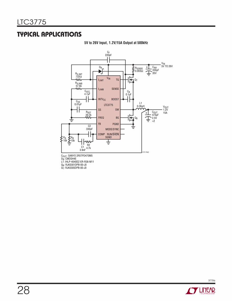
LTC3775
283775fa
TYPICAL APPLICATIONS5V to 26V Input, 1.2V/15A Output at 500kHz
CB0.1μF
CF220pF
L10.36μH
COUT470μF2.5V
2
CIN1330μF35V
VIN5V TO 26V
VOUT1.2V15A
3775 TA02
CVCC4.7μF
C2330pF
C13.9nF
RILIMB57.6k
RSET39.2k
R24.7k
RB10k
COUT: SANYO 2R5TPD470M5DB: CMDSH4EL1: IHLP-4040DZ-ER-R36-M11QB: RJK0301DPB-00-J0QT: RJK0305DPB-00-J0
RA10k
RSENSE0.003Ω
RILIMT732Ω
DB
CSS0.01μF
TG QT
QB
VIN
LTC3775
SGND
SENSE
ILIMT
ILIMB
INTVCC
SS
BG
PGND
MODE/SYNC
RUN/SHDNCOMP
BOOST
SW
FREQ
FB
+
+

LTC3775
293775fa
8V to 36V Input, 2.5V/10A Output at 500kHz
L11.2μH
COUT330μF4V
3
CIN1330μF35V
VIN8V TO 36V
VOUT2.5V10A
3775 TA03
CVCC4.7μF
CB0.1μF
C2330pFC3
1500pF
C12200pF
RILIMB133k
RSET39.2k
R215k
RB3.16k
COUT: SANYO 4TPD330MDB: CMDSH4EL1: TOKO FDA1254-1R2MQB,QT: INFINEON BSZ097N04LS
RA10k
R3390Ω
DB
R443.2k
RILIMT464Ω RSENSE
0.003ΩR510k
CSS0.01μF
ILIMT
QT
CF220pF
QB
VIN
LTC3775
SGND
SENSE
BOOST
ILIMB
INTVCC
SS
BG
PGND
MODE/SYNC
COMP
TG
SW
FREQ
RUN/SHDN
FB
+
+
Load StepEffi ciency and Power Loss
vs Load Current Start-Up
IL10A/DIV
VOUT(AC)100mV/DIV
50μs/DIV 3775 TA03cVIN = 12VVOUT = 2.5VLOAD = 0A TO 10A TO 0AMODE = 0VSW FREQ = 500kHz
LOAD CURRENT (A)
0.01
40
EFF
ICIE
NC
Y (
%)
PO
WER
LO
SS
(W)
50
60
70
80
0.1 1 10
3775 TA03b
30
20
10
0
90
100
4
3
2
1
0
5VIN = 12VVOUT = 2.5VCONTINUOUS MODESW FREQ = 500kHz
EFFICIENCY
POWER LOSS
IL5A/DIV
VOUT1V/DIV
VSS1V/DIV
2ms/DIV 3775 TA03dVIN = 12VVOUT = 2.5VCSS = 0.01μFMODE = 0VSW FREQ = 500kHz
SWITCHOVERFROM PULSE-SKIPPING TO CONTINUOUSMODE
TYPICAL APPLICATIONS

LTC3775
303775fa
TYPICAL APPLICATIONS24V Input, 12V/5A Output at 500kHz
CB0.1μF
L14.7μH
COUT68μF16V
2
CIN1330μF35V
VIN24V
VOUT12V5A
3775 TA04
CVCC4.7μF
C2330pF
C13.3nF
RILIMB56.2k
RSET39.2k
R27.68k
RB10k
COUT: SANYO 16TQC68MDB: CMDSH4EL1: IHLP-4040DZ-ER-4R7-M11QB, QT: RJK0305DPB-00-JO
RA191k
R32.05k
C3330pF
RILIMT1.24k
R469.8k
R510k
DB
CSS0.01μF
TG QT
QB
VIN
LTC3775
SGND
SENSE
ILIMT
ILIMB
INTVCC
SS
BG
PGND
MODE/SYNC
COMP
BOOST
SW
FREQ
RUN/SHDN
FB
+
+
Load StepEffi ciency and Power Loss
vs Load Current Start-Up
LOAD CURRENT (A)
30
EFF
ICIE
NC
Y (
%)
PO
WER
LO
SS
(W)
90
100
20
10
80
50
70
60
40
0.01 1 10
3775 TA04b
0
1.0
2.5
0.5
2.0
1.5
00.1
EFFICIENCY
POWER LOSS
VIN = 24VVOUT = 12VCONTINUOUS MODESW FREQ = 500kHz
IL5A/DIV
VOUT(AC)200mV/DIV
50μs/DIV 3775 TA04cVIN = 24VVOUT = 12VLOAD = 0A TO 5A TO 0AMODE = 0VSW FREQ = 500kHz
IL5A/DIV
VOUT5V/DIV
VSS1V/DIV
2ms/DIV 3775 TA04dVIN = 24VVOUT = 12VCSS = 0.01μFMODE = 0VSW FREQ = 500kHz
SWITCHOVERFROM PULSE-SKIPPING TO CONTINUOUSMODE

LTC3775
313775fa
PACKAGE DESCRIPTIONUD Package
16-Lead Plastic QFN (3mm × 3mm)(Reference LTC DWG # 05-08-1691)
3.00 0.10(4 SIDES)
RECOMMENDED SOLDER PAD PITCH AND DIMENSIONS
1.45 0.05(4 SIDES)
NOTE:1. DRAWING CONFORMS TO JEDEC PACKAGE OUTLINE MO-220 VARIATION (WEED-2)2. DRAWING NOT TO SCALE3. ALL DIMENSIONS ARE IN MILLIMETERS4. DIMENSIONS OF EXPOSED PAD ON BOTTOM OF PACKAGE DO NOT INCLUDE MOLD FLASH. MOLD FLASH, IF PRESENT, SHALL NOT EXCEED 0.15mm ON ANY SIDE5. EXPOSED PAD SHALL BE SOLDER PLATED6. SHADED AREA IS ONLY A REFERENCE FOR PIN 1 LOCATION ON THE TOP AND BOTTOM OF PACKAGE
PIN 1TOP MARK(NOTE 6)
0.40 0.10
BOTTOM VIEW—EXPOSED PAD
1.45 0.10(4-SIDES)
0.75 0.05R = 0.115
TYP
0.25 0.05
1
PIN 1 NOTCH R = 0.20 TYPOR 0.25 45 CHAMFER
15 16
2
0.50 BSC
0.200 REF
2.10 0.05
3.50 0.05
0.70 0.05
0.00 – 0.05
(UD16) QFN 0904
0.25 0.050.50 BSC
PACKAGE OUTLINE

LTC3775
323775fa
PACKAGE DESCRIPTION
MSOP (MSE16) 0608 REV A
0.53 0.152
(.021 .006)
SEATINGPLANE
0.18
(.007)
1.10
(.043)MAX
0.17 – 0.27
(.007 – .011)TYP
0.86
(.034)REF
0.50
(.0197)BSC
16
16151413121110
1 2 3 4 5 6 7 8
9
9
1 8
NOTE:1. DIMENSIONS IN MILLIMETER/(INCH)2. DRAWING NOT TO SCALE3. DIMENSION DOES NOT INCLUDE MOLD FLASH, PROTRUSIONS OR GATE BURRS. MOLD FLASH, PROTRUSIONS OR GATE BURRS SHALL NOT EXCEED 0.152mm (.006") PER SIDE4. DIMENSION DOES NOT INCLUDE INTERLEAD FLASH OR PROTRUSIONS. INTERLEAD FLASH OR PROTRUSIONS SHALL NOT EXCEED 0.152mm (.006") PER SIDE5. LEAD COPLANARITY (BOTTOM OF LEADS AFTER FORMING) SHALL BE 0.102mm (.004") MAX
0.254
(.010)0 – 6 TYP
DETAIL “A”
DETAIL “A”
GAUGE PLANE
5.23(.206)MIN
3.20 – 3.45(.126 – .136)
0.889 0.127(.035 .005)
RECOMMENDED SOLDER PAD LAYOUT
0.305 0.038(.0120 .0015)
TYP
0.50(.0197)
BSC
BOTTOM VIEW OF
EXPOSED PAD OPTION
2.845 0.102
(.112 .004)
2.845 0.102
(.112 .004)
4.039 0.102
(.159 .004)(NOTE 3)
1.651 0.102
(.065 .004)
1.651 0.102
(.065 .004)
0.1016 0.0508
(.004 .002)
3.00 0.102
(.118 .004)(NOTE 4)
0.280 0.076
(.011 .003)REF
4.90 0.152
(.193 .006)
DETAIL “B”
DETAIL “B”
CORNER TAIL IS PART OF
THE LEADFRAME FEATURE.
FOR REFERENCE ONLY
NO MEASUREMENT PURPOSE
0.12 REF
0.35REF
MSE Package16-Lead Plastic MSOP, Exposed Die Pad
(Reference LTC DWG # 05-08-1667 Rev A)
LTC3775
333775fa
Information furnished by Linear Technology Corporation is believed to be accurate and reliable. However, no responsibility is assumed for its use. Linear Technology Corporation makes no representa-tion that the interconnection of its circuits as described herein will not infringe on existing patent rights.
REVISION HISTORYREV DATE DESCRIPTION PAGE NUMBER
A 8/10 MSOP package added. Refl ected throughout the data sheet. 1 to 34
LTC3775
343775fa
Linear Technology Corporation1630 McCarthy Blvd., Milpitas, CA 95035-7417 (408) 432-1900 ● FAX: (408) 434-0507 ● www.linear.com © LINEAR TECHNOLOGY CORPORATION 2009
LT 0810 REV A • PRINTED IN USA
RELATED PARTSPART NUMBER DESCRIPTION COMMENTS
LTC3854 Small Footprint Wide VIN Range Synchronous Step-Down DC/DC Controller
Fixed 400kHz Operating Frequency, 4.5V ≤ VIN ≤ 38V, 0.8V ≤ VOUT ≤ 5.25V, 2mm × 3mm QFN-12
LTC3851A/LTC3851A-1
Wide VIN Range Synchronous Step-Down DC/DC Controller Phase-Lockable Fixed Operating Frequency 250kHz to 750kHz, 4V ≤ VIN ≤ 38V, 0.8V ≤ VOUT ≤ 5.25V, MSOP-16E, 3mm × 3mm QFN-16, SSOP-16
LTC3878/ LTC3879
No RSENSE™ Constant On-Time Synchronous Step-Down DC/DC Controller
Very Fast Transient Response, tON(MIN) = 43ns, 4V ≤ VIN ≤ 38V, 0.8V ≤ VOUT ≤ 0.9VIN, SSOP-16, MSOP-16E, 3mm × 3mm QFN-16
LTC3850/LTC3850-1/ LTC3850-2
Dual 2-Phase, High Effi ciency Synchronous Step-Down DC/DC Controllers, RSENSE or DCR Current Sensing and Tracking
Phase-Lockable Fixed Operating Frequency 250kHz to 780kHz, 4V ≤ VIN ≤ 30V, 0.8V ≤ VOUT ≤ 5.25V
LTC3860 Dual, Multiphase Synchronous Step-Down DC/DC Controller with Diff Amp and 3-State Output Drive
Operates with Power Blocks, DRMOS Devices or External MOSFETs 3V ≤ VIN ≤ 24V, tON(MIN) = 20ns
LTC3853 Triple Output, Multiphase Synchronous Step-Down DC/DC Controller, RSENSE or DCR Current Sensing and Tracking
Phase-Lockable Fixed Operating Frequency 250kHz to 750kHz, 4V ≤ VIN ≤ 24V, VOUT Up to 13.5V
TYPICAL APPLICATIONWide Input Range CPU Power Supply (Refer to Demo Board DC1290A-B)
TG
VIN
VIN
LTC3775
PGND
SENSE
ILIMT
ILIMB
INTVCC
INTVCC CMDSH-4E
RS1 (OPT)
BSC016NO4LSG Q2
D1(OPT)
L1WURTH
7443141101.1μH
Q4(OPT)
Q3(OPT)
1
4
2 3
5
Q1
INFINEONBSC093NO4LSG
VOUT
INTVCC
RUNRUN
MODE
SSC610nFR16
(OPT)
R956.2k
BG
MODE/SYNC
COMP
BOOST
SW
FREQ
FB
1
2
16
C3330pF
C20.022μF
C8 100pF
CIN5 0.1μF50V
C10.1μF
R610k1%
R11.62k
R150Ω
R52k
C44700pF R2
31.6k
RS2 0Ω
RSNS2(OPT)RSNS1
0.004Ω
R3 4.7
R80Ω
R71.82k
5
SGND
7
15
4
6
3
11
14
10
17
9
12
8
13R410k1%
C54.7μF10V
1
4
2 3
5
3775 TA05
COUT4100μF6.3V
COUT1470μF4VSANYOPOSCAP4TPF470MU
VOUT
VOUT+
VOUT
1.2V/10A
GND
VOUT–
COUT2470μF4V
COUT5(OPT)
E3
J3
J4
E4
COUT31μF6.3VX5R
+ +
+
CIN24.7μF50V
CIN34.7μF50V
VIN+
VIN
5V TO 36V
GND
VIN–
CIN4(OPT)
E1
J1
J2
E2
CIN1100μF50V
+
VIN = 5V TO 36VVOUT = 1.2V/10AFS = 350kHz
INTVCC
1
2
3
4
JP1
MODE
R13 1k
MODE
PULSE-SKIPPING
SYNC
FCC
SGND
SYNC
E8
E6
VOUT
VIN
1
2
3
JP2
C7(OPT)
R12(OPT)
R14(OPT)
ON
OFF
RUN
RUNE7
D2


![High-Accurate Step-Down DC-DC Converter with …...[AP3440] 016008997-E-00 2016/10-1-1. General Description The AP3440 is a synchronous rectification PWM control step-down DC-DC converter](https://img.dokumen.tips/doc/110x75/5ea7b135a93cbf2b573fb244/high-accurate-step-down-dc-dc-converter-with-ap3440-016008997-e-00-201610-1-1.jpg)