Embed Size (px)
Citation preview
LTC3610
�3610ff
0.47µH
4.7µF
10µF×3
VIN4V TO 24V
VOUT2.5V12A
3610 TA01a
604k0.1µF ION
VIN
SW
BOOST
RUN/SS
ITH
VON
SGND INTVCC
FCB
PGND
VFB
VRNG
0.22µF 100µF×2
31.83k
LTC3610
470pF
EXTVCC
PGOOD
30.1k
9.5k
100pF
LOAD CURRENT (A)0.01
EFFI
CIEN
CY (%
)
POWER LOSS (m
W)
80
90
3610 TA01b
70
50
60
85
95
75
55
65
0.1 1 10
100
1000
100
1
10
10000
VOUT = 2.5V
POWER LOSS 12V
POWER LOSS 5V
VIN = 12V
VIN = 5V
Features
applications
Description
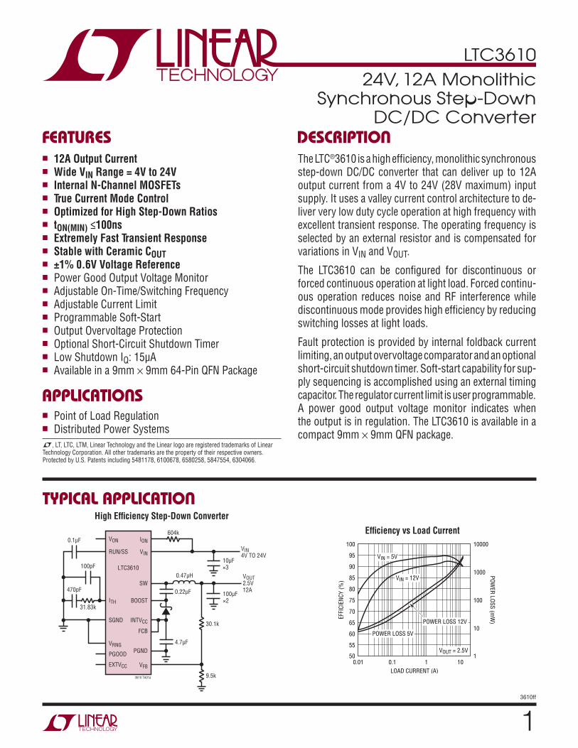
24V, 12A Monolithic Synchronous Step-Down
DC/DC Converter
The LTC®3610 is a high efficiency, monolithic synchronous step-down DC/DC converter that can deliver up to 12A output current from a 4V to 24V (28V maximum) input supply. It uses a valley current control architecture to de-liver very low duty cycle operation at high frequency with excellent transient response. The operating frequency is selected by an external resistor and is compensated for variations in VIN and VOUT.
The LTC3610 can be configured for discontinuous or forced continuous operation at light load. Forced continu-ous operation reduces noise and RF interference while discontinuous mode provides high efficiency by reducing switching losses at light loads.
Fault protection is provided by internal foldback current limiting, an output overvoltage comparator and an optional short-circuit shutdown timer. Soft-start capability for sup-ply sequencing is accomplished using an external timing capacitor. The regulator current limit is user programmable. A power good output voltage monitor indicates when the output is in regulation. The LTC3610 is available in a compact 9mm × 9mm QFN package.
■ 12AOutputCurrent■ WideVINRange=4Vto24V■ InternalN-ChannelMOSFETs■ TrueCurrentModeControl■ OptimizedforHighStep-DownRatios■ tON(MIN)≤100ns■ ExtremelyFastTransientResponse■ StablewithCeramicCOUT■ ±1%0.6VVoltageReference■ Power Good Output Voltage Monitor■ Adjustable On-Time/Switching Frequency■ Adjustable Current Limit■ Programmable Soft-Start■ Output Overvoltage Protection■ Optional Short-Circuit Shutdown Timer■ Low Shutdown IQ: 15µA■ Available in a 9mm × 9mm 64-Pin QFN Package
■ Point of Load Regulation■ Distributed Power Systems
HighEfficiencyStep-DownConverterEfficiencyvsLoadCurrent
typical application
L, LT, LTC, LTM, Linear Technology and the Linear logo are registered trademarks of Linear Technology Corporation. All other trademarks are the property of their respective owners. Protected by U.S. Patents including 5481178, 6100678, 6580258, 5847554, 6304066.

LTC3610
�3610ff
absolute MaxiMuM ratings
Input Supply Voltage (VIN, ION) .................. 28V to –0.3VBoosted Topside Driver Supply Voltage
(BOOST) ................................................ 34V to –0.3V SW Voltage ............................................ 28V to –0.3V
INTVCC, EXTVCC, (BOOST – SW), RUN/SS, PGOOD Voltages ...................................... 7V to –0.3V
FCB, VON, VRNG Voltages ............ INTVCC + 0.3V to –0.3VITH, VFB Voltages ....................................... 2.7V to –0.3VOperating Temperature Range
(Note 4) ............................................. –40°C to 125°CJunction Temperature (Note 2) ............................. 125°CStorage Temperature Range ................... –55°C to 125°C
(Note1)
SYMBOL PARAMETER CONDITIONS MIN TYP MAX UNITS
MainControlLoop
VIN Operating Input Voltage Range 4 24 V
IQ Input DC Supply Current Normal Shutdown Supply Current
900 15
2000 30
µA µA
VFB Feedback Reference Voltage ITH = 1.2V (Note 3) ● 0.594 0.600 0.606 V
ΔVFB(LINEREG) Feedback Voltage Line Regulation VIN = 4V to 28V, ITH = 1.2V (Note 3) 0.002 %/V
pin conFiguration
TOP VIEW
WP PACKAGE64-LEAD (9mm × 9mm) QFN MULTIPAD
PGND 1
PGND 2
PGND 3
SW 4
SW 5
SW 6
SW 7
SW 8
SW 9
SW 10
SW 11
PVIN 12
PVIN 13
PVIN 14
PVIN 15
PVIN 16
48 SGND
47 SGND
46 SGND
45 SGND
44 EXTVCC
43 VFB
42 SGND
41 ION
40 SGND
39 FCB
38 ITH
37 VRNG
36 PGOOD
35 VON
34 SGND
33 SGND
PVIN
17
PVIN
18
PVIN
19
PVIN
20
PVIN
21
PVIN
22
PVIN
23
PVIN
24
PVIN
25
SW 2
6
NC 2
7
SGND
28
BOOS
T 29
RUN/
SS 3
0
SGND
31
SGND
32
64 P
GND
63 P
GND
62 P
GND
61 P
GND
60 P
GND
59 P
GND
58 P
GND
57 P
GND
56 P
GND
55 S
W
54 IN
TVCC
53 IN
TVCC
52 S
V IN
51 S
V IN
50 S
GND
49 S
GND
68SGND
67PVIN
66SW
65PGND
TJMAX = 125°C, θJA = 28°C/W
orDer inForMationLEADFREEFINISH TAPEANDREEL PARTMARKING* PACKAGEDESCRIPTION TEMPERATURERANGELTC3610EWP#PBF LTC3610EWP#TRPBF LTC3610WP 64-Lead (9mm × 9mm) Plastic QFN –40°C to 125°C
LTC3610IWP#PBF LTC3610IWP#TRPBF LTC3610WP 64-Lead (9mm × 9mm) Plastic QFN –40°C to 125°C
LEADBASEDFINISH TAPEANDREEL PARTMARKING* PACKAGEDESCRIPTION TEMPERATURERANGELTC3610EWP LTC3610EWP#TR LTC3610WP 64-Lead (9mm × 9mm) Plastic QFN –40°C to 125°C
LTC3610IWP LTC3610IWP#TR LTC3610WP 64-Lead (9mm × 9mm) Plastic QFN –40°C to 125°C
Consult LTC Marketing for parts specified with wider operating temperature ranges.*The temperature grade is identified by a label on the shipping container.For more information on lead free part marking, go to: http://www.linear.com/leadfree/ For more information on tape and reel specifications, go to: http://www.linear.com/tapeandreel/
electrical characteristics The●denotesthespecificationswhichapplyoverthefulloperatingtemperaturerange,otherwisespecificationsareatTA=25°C(Note4).VIN=15Vunlessotherwisenoted.

LTC3610
�3610ff
electrical characteristics The●denotesthespecificationswhichapplyoverthefulloperatingtemperaturerange,otherwisespecificationsareatTA=25°C(Note4).VIN=15Vunlessotherwisenoted.
SYMBOL PARAMETER CONDITIONS MIN TYP MAX UNITS
ΔVFB(LOADREG) Feedback Voltage Load Regulation ITH = 0.5V to 1.9V (Note 3) –0.05 –0.3 %
IFB Feedback Input Current VFB = 0.6V –5 ±50 nA
gm(EA) Error Amplifier Transconductance ITH = 1.2V (Note 3) ● 1.4 1.7 2 mS
VFCB Forced Continuous Threshold ● 0.54 0.6 0.66 V
IFCB Forced Continuous Pin Current VFCB = 0.6V –1 –2 µA
tON On-Time ION = 60µA, VON = 1.5V ION = 60µA, VON = 0V
170 250 120
310 ns ns
tON(MIN) Minimum On-Time ION = 180µA, VON = 0V 60 100 ns
tOFF(MIN) Minimum Off-Time ION = 30µA, VON = 1.5V 290 500 ns
IVALLEY(MAX) Maximum Valley Current VRNG = 0.5V, VFB = 0.56V, FCB = 0V VRNG = 0V, VFB = 0.56V, FCB = 0V
●
●
7 10
16 19
A A
IVALLEY(MIN) Maximum Reverse Valley Current VRNG = 0.5V, VFB = 0.64V, FCB = 0V VRNG = 0V, VFB = 0.64V, FCB = 0V
–6 –9
A A
ΔVFB(OV) Output Overvoltage Fault Threshold 7 10 13 %
VRUN/SS(ON) RUN Pin Start Threshold ● 0.8 1.5 2 V
VRUN/SS(LE) RUN Pin Latchoff Enable Threshold RUN/SS Pin Rising 4 4.5 V
VRUN/SS(LT) RUN Pin Latchoff Threshold RUN/SS Pin Falling 3.5 4.2 V
IRUN/SS(C) Soft-Start Charge Current VRUN/SS = 0V –0.5 –1.2 –3 µA
IRUN/SS(D) Soft-Start Discharge Current VRUN/SS = 4.5V, VFB = 0V 0.8 1.8 3 µA
VIN(UVLO) Undervoltage Lockout VIN Falling ● 3.4 3.9 V
VIN(UVLOR) Undervoltage Lockout Release VIN Rising ● 3.5 4 V
RDS(ON) Top Switch On-Resistance Bottom Switch On-Resistance
12 6.5
16 10
mΩ mΩ
InternalVCCRegulator
VINTVCC Internal VCC Voltage 6V < VIN < 28V, VEXTVCC = 4V ● 4.7 5 5.5 V
ΔVLDO(LOADREG) Internal VCC Load Regulation ICC = 0mA to 20mA, VEXTVCC = 4V –0.1 ±2 %
VEXTVCC EXTVCC Switchover Voltage ICC = 20mA, VEXTVCC Rising ● 4.5 4.7 V
ΔVEXTVCC EXTVCC Switch Drop Voltage ICC = 20mA, VEXTVCC = 5V 150 300 mV
ΔVEXTVCC(HYS) EXTVCC Switchover Hysteresis 500 mV
PGOODOutput
ΔVFBH PGOOD Upper Threshold VFB Rising 7 10 13 %
ΔVFBL PGOOD Lower Threshold VFB Falling –7 –10 –13 %
ΔVFB(HYS) PGOOD Hysteresis VFB Returning 1 2.5 %
VPGL PGOOD Low Voltage IPGOOD = 5mA 0.15 0.4 V
Note1: Stresses beyond those listed under Absolute Maximum Ratings may cause permanent damage to the device. Exposure to any Absolute Maximum Rating condition for extended periods may affect device reliability and lifetime.Note2: TJ is calculated from the ambient temperature TA and power dissipation PD as follows: TJ = TA + (PD • 28°C/W) (θJA is simulated per JESD51-7 high effective thermal conductivity test board) θJC = 0.24°C/W (θJC is simulated when heat sink is applied at the bottom of the package).
Note3: The LTC3610 is tested in a feedback loop that adjusts VFB to achieve a specified error amplifier output voltage (ITH).Note4: The LTC3610 is tested under pulsed load conditions such that TJ ≈ TA. The LTC3610E is guaranteed to meet performance specifications from 0°C to 125°C. Specifications over the –40°C to 125°C operating temperature range are assured by design, characterization and correlation with statistical process controls. The LTC3610I is guaranteed over the full –40°C to 125°C operating junction temperature range. Note that the maximum ambient temperature is determined by specific operating conditions in conjunction with board layout, the rated package thermal resistance and other environmental factors.
LTC3610
�3610ff
LOAD CURRENT (A)0.001
EFFI
CIEN
CY (%
)
70
80
10
3610 G04
60
500.01 0.1 1
100
90
DISCONTINUOUSMODE
CONTINUOUSMODE
VIN = 12VVOUT = 2.5V
EXTVCC = 5VFIGURE 6 CIRCUIT
INPUT VOLTAGE (V)5
80
EFFI
CIEN
CY (%
)
85
90
95
100
10 15 20
3610 G05
25
ILOAD = 1A
ILOAD = 10A
FCB = 5VFIGURE 6 CIRCUIT
INPUT VOLTAGE (V)5
FREQ
UENC
Y (k
Hz)
480
520
25
3610 G06
440
40010 15 20
640
600
560
ILOAD = 10A
FCB = 0VFIGURE 6 CIRCUIT
ILOAD = 0A
LOAD CURRENT (A)0
ΔV O
UT (%
)
8
3610 G08
–0.80
–0.60
–0.40
–0.20
0.60
0.40
0.20
0
2 4 6 1210
0.80FIGURE 6 CIRCUIT
LOAD CURRENT (A)0
I TH
VOLT
AGE
(V)
1.0
1.5
3610 G09
0.5
03 6 9 12
2.5
2.0
CONTINUOUSMODE
DISCONTINUOUSMODE
FIGURE 6 CIRCUIT
LOAD CURRENT (A)0
0
FREQ
UENC
Y (k
Hz)
50100150200250300350400450500550600650
2 4 6 8
3610 G07
1210
CONTINUOUS MODE
DISCONTINUOUS MODE
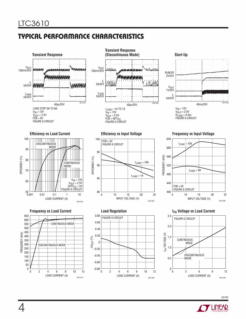
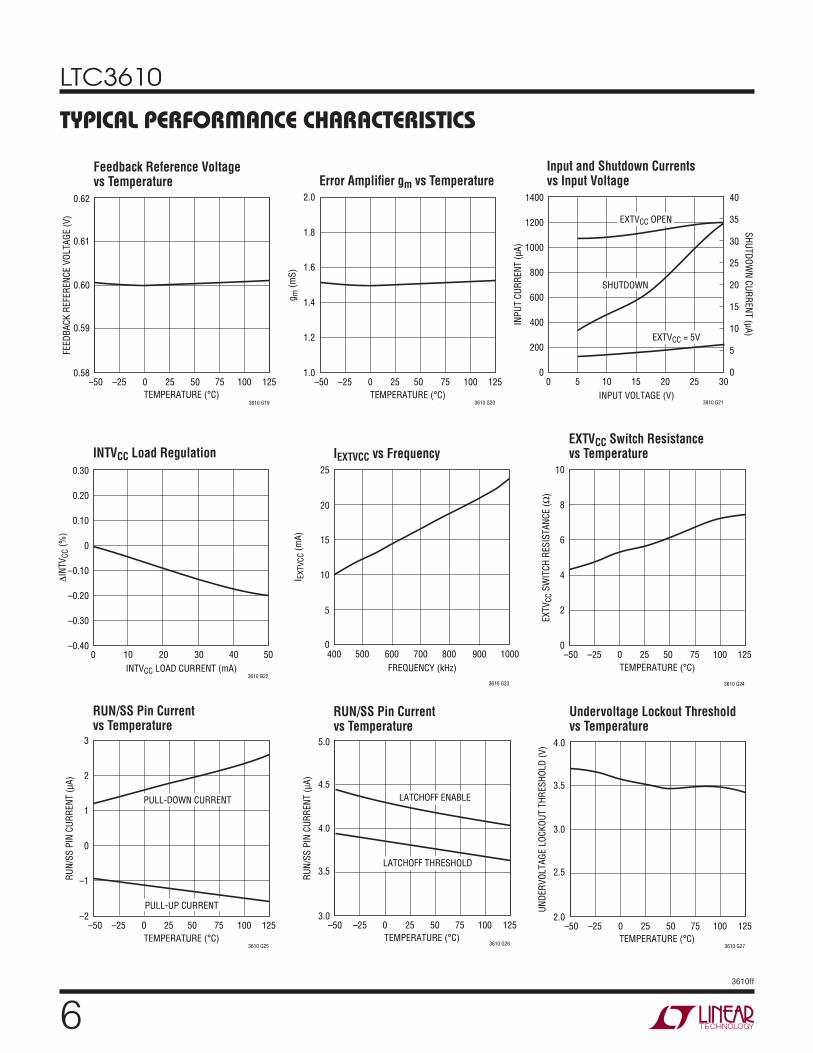
typical perForMance characteristics
TransientResponse
TransientResponse(DiscontinuousMode)
Start-Up
EfficiencyvsLoadCurrent
EfficiencyvsInputVoltage
FrequencyvsInputVoltage
FrequencyvsLoadCurrent
LoadRegulation
ITHVoltagevsLoadCurrent
LOAD STEP 0A TO 8AVIN = 12VVOUT = 2.5VFCB = 0VFIGURE 6 CIRCUIT
3610 G0140µs/DIV
VOUT100mV/DIV
IL5A/DIV
ILOAD5A/DIV
ILOAD = 1A TO 7AVIN = 12VVOUT = 2.5VFCB = INTVCCFIGURE 6 CIRCUIT
3610 G0240µs/DIV
VOUT100mV/DIV
IL5A/DIV
ILOAD5A/DIV
VIN = 12VVOUT = 2.5VRLOAD = 0.5ΩFIGURE 6 CIRCUIT
3610 G0340ms/DIV
RUN/SS2V/DIV
VOUT1V/DIV
IL5A/DIV

LTC3610
�3610ff
INPUT VOLTAGE (V)4
MAX
IMUM
VAL
LEY
CURR
ENT
(A)
18
16
14
12
10
3610 G17
4
6
8
7 10 13 16 19 282522
RUN/SS VOLTAGE (V)1.65
0
MAX
IMUM
VAL
LEY
CURR
ENT
LIM
IT (A
)
3
6
9
12
18
15
1.90 2.15 2.65 2.90 3.15 3.402.40
3610 G15
ITH VOLTAGE (V)0
–10
LOAD
CUR
RENT
(A)
–5
0
5
20
15
10
25
0.5 1.0 1.5 2.0
3610 G10
2.5 3.0
VRNG = 1V
0.7V
0.5V
ION CURRENT (µA)1
10
ON-T
IME
(ns)
100
1000
10000
10 100
3610 G11
VVON = 0V
VON VOLTAGE (V)0
ON-T
IME
(ns)
400
600
3610 G12
200
01 2 3
1000ION = 30µA
800
TEMPERATURE (°C)–50
ON-T
IME
(ns)
200
250
300
25 75
3610 G13
150
100
–25 0 50 100 125
50
0
IION = 30µAVVON = 0V
VFB (V)0
0
MAX
IMUM
VAL
LEY
CURR
ENT
LIM
IT (A
)
5
10
15
0.1 0.2 0.3 0.4 0.5 0.6
3610 G18
VRNG VOLTAGE (V)0.5
10
MAX
IMUM
VAL
LEY
CURR
ENT
LIM
IT (A
)
12
14
16
18
20
22
24
0.6 0.7 0.8
3610 G14
0.9 1.0
TEMPERATURE (°C)–50 –25
0
MAX
IMUM
VAL
LEY
CURR
ENT
LIM
IT (A
)
5
20
0 50 75
3610 G16
15
10
25 100 125
typical perForMance characteristics
LoadCurrentvsITHVoltageandVRNG
On-TimevsIONCurrent
On-TimevsVONVoltage
On-TimevsTemperature
MaximumValleyCurrentLimitinFoldback
MaximumValleyCurrentLimitvsVRNGVoltage
MaximumValleyCurrentLimitvsRUN/SSVoltage
MaximumValleyCurrentLimitvsTemperature
InputVoltagevsMaximumValleyCurrent
LTC3610
�3610ff
TEMPERATURE (°C)–50 –25
0
EXTV
CC S
WIT
CH R
ESIS
TANC
E (Ω
)
4
10
0 50 75
3610 G24
2
8
6
25 100 125
TEMPERATURE (°C)–50 –25
–2
RUN/
SS P
IN C
URRE
NT (µ
A)
0
3
0 50 75
3610 G25
–1
2
1
25 100 125
PULL-UP CURRENT
PULL-DOWN CURRENT
TEMPERATURE (°C)–50 –25
1.0
g m (m
S)1.4
2.0
0 50 75
3610 G20
1.2
1.8
1.6
25 100 125INPUT VOLTAGE (V)
0
INPU
T CU
RREN
T (µ
A)
SHUTDOWN CURRENT (µA)
800
1000
1400
1200
15 25
3610 G21
600
400
5 10 20 30
200
0
30
25
15
5
40
35
20
10
0
EXTVCC OPEN
EXTVCC = 5V
SHUTDOWN
INTVCC LOAD CURRENT (mA)0
ΔIN
TVCC
(%)
0.10
0.20
0.30
40
3610 G22
0
–0.20
–0.10
–0.40
–0.30
10 20 30 50
typical perForMance characteristics
ErrorAmplifiergmvsTemperature
InputandShutdownCurrentsvsInputVoltage
INTVCCLoadRegulation
EXTVCCSwitchResistancevsTemperature
IEXTVCCvsFrequency
RUN/SSPinCurrentvsTemperature
RUN/SSPinCurrentvsTemperature
UndervoltageLockoutThresholdvsTemperature
TEMPERATURE (°C)–50
3.0
RUN/
SS P
IN C
URRE
NT (µ
A)
3.5
4.0
4.5
5.0
–25 0 25 50
3610 G26
75 100 125
LATCHOFF ENABLE
LATCHOFF THRESHOLD
TEMPERATURE (°C)–50
2.0
UNDE
RVOL
TAGE
LOC
KOUT
THR
ESHO
LD (V
)
2.5
3.0
3.5
4.0
–25 0 25 50
3610 G27
75 100 125
TEMPERATURE (°C)–50
0.58
FEED
BACK
REF
EREN
CE V
OLTA
GE (V
)
0.59
0.60
0.61
0.62
–25 0 25 50
3610 G19
75 100 125
FeedbackReferenceVoltagevsTemperature
FREQUENCY (kHz)400
I EXT
VCC
(mA) 15
20
25
700 900
3610 G23
10
5
500 600 800 10000
LTC3610
�3610ff
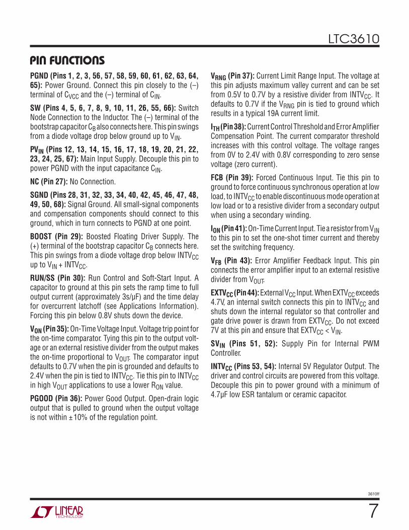
pin FunctionsPGND(Pins1,2,3,56,57,58,59,60,61,62,63,64,65): Power Ground. Connect this pin closely to the (–) terminal of CVCC and the (–) terminal of CIN.
SW(Pins4,5,6,7,8,9,10,11,26,55,66): Switch Node Connection to the Inductor. The (–) terminal of the bootstrap capacitor CB also connects here. This pin swings from a diode voltage drop below ground up to VIN.
PVIN(Pins12,13,14,15,16,17,18,19,20,21,22,23,24,25,67): Main Input Supply. Decouple this pin to power PGND with the input capacitance CIN.
NC(Pin27): No Connection.
SGND(Pins28,31,32,33,34,40,42,45,46,47,48,49,50,68): Signal Ground. All small-signal components and compensation components should connect to this ground, which in turn connects to PGND at one point.
BOOST (Pin 29): Boosted Floating Driver Supply. The (+) terminal of the bootstrap capacitor CB connects here. This pin swings from a diode voltage drop below INTVCC up to VIN + INTVCC.
RUN/SS (Pin30): Run Control and Soft-Start Input. A capacitor to ground at this pin sets the ramp time to full output current (approximately 3s/µF) and the time delay for overcurrent latchoff (see Applications Information). Forcing this pin below 0.8V shuts down the device.
VON(Pin35): On-Time Voltage Input. Voltage trip point for the on-time comparator. Tying this pin to the output volt-age or an external resistive divider from the output makes the on-time proportional to VOUT. The comparator input defaults to 0.7V when the pin is grounded and defaults to 2.4V when the pin is tied to INTVCC. Tie this pin to INTVCC in high VOUT applications to use a lower RON value.
PGOOD(Pin36): Power Good Output. Open-drain logic output that is pulled to ground when the output voltage is not within ±10% of the regulation point.
VRNG(Pin37): Current Limit Range Input. The voltage at this pin adjusts maximum valley current and can be set from 0.5V to 0.7V by a resistive divider from INTVCC. It defaults to 0.7V if the VRNG pin is tied to ground which results in a typical 19A current limit.
ITH(Pin38): Current Control Threshold and Error Amplifier Compensation Point. The current comparator threshold increases with this control voltage. The voltage ranges from 0V to 2.4V with 0.8V corresponding to zero sense voltage (zero current).
FCB(Pin39): Forced Continuous Input. Tie this pin to ground to force continuous synchronous operation at low load, to INTVCC to enable discontinuous mode operation at low load or to a resistive divider from a secondary output when using a secondary winding.
ION(Pin41): On-Time Current Input. Tie a resistor from VIN to this pin to set the one-shot timer current and thereby set the switching frequency.
VFB (Pin 43): Error Amplifier Feedback Input. This pin connects the error amplifier input to an external resistive divider from VOUT.
EXTVCC(Pin44): External VCC Input. When EXTVCC exceeds 4.7V, an internal switch connects this pin to INTVCC and shuts down the internal regulator so that controller and gate drive power is drawn from EXTVCC. Do not exceed 7V at this pin and ensure that EXTVCC < VIN.
SVIN (Pins 51, 52): Supply Pin for Internal PWM Controller.
INTVCC(Pins53,54): Internal 5V Regulator Output. The driver and control circuits are powered from this voltage. Decouple this pin to power ground with a minimum of 4.7µF low ESR tantalum or ceramic capacitor.

LTC3610
�3610ff
Functional DiagraM
0.7V
1.4V
VRNG
–
+
–+
– +
– +
–
+
IONVON
ICMP
0.7V
FCB EXTVCC SVIN
1µA
RON
VVONIION
tON = (10pF) R
S Q
20k
IREV
×(0.5 TO 2)
1V
SHDN
SWITCHLOGIC
ON
FCNT
0.6V
–+
4.7V
OV
1240k
0.4V
ITH
CSS
EA
SS
0.6V
+–
+–×3.3
RUN/SS3610 FD
SGND
R1
RUNSHDN
PGND
PGOOD
VFB
SW
PVIN
CIN
BOOST
M1
M2
INTVCC
–
+
–
+
UV
0.54V
OV
0.66V
6V
0.6VREF
5VREG
R2
2.4V
37
35 41 39 44
29
NC27
4, 5, 6, 7, 8, 9,10, 11, 26, 55, 66
12, 13, 14, 15,16, 17, 18, 19,20, 21, 22, 23,24, 25, 67
53, 54
51, 52
1, 2, 3, 56, 57, 58, 59, 60, 61, 62, 63, 64, 65
28, 31, 32, 33, 34,40, 42, 45, 46, 47,48, 49, 50, 68
36
43
3038
VOUT
L1
COUT
CVCC
+
Q1Q3
Q4Q2
0.8V
ITHBQ6
CB
DB
F
1.2µA

LTC3610
�3610ff
operationMainControlLoop
The LTC3610 is a high efficiency monolithic synchronous, step-down DC/DC converter utilizing a constant on-time, current mode architecture. It operates from an input voltage range of 4V to 24V and provides a regulated output voltage at up to 12A of output current. The internal synchronous power switch increases efficiency and eliminates the need for an external Schottky diode. In normal operation, the top MOSFET is turned on for a fixed interval determined by a one-shot timer OST. When the top MOSFET is turned off, the bottom MOSFET is turned on until the current comparator ICMP trips, restarting the one-shot timer and initiating the next cycle. Inductor current is determined by sensing the voltage between the PGND and SW pins using the bottom MOSFET on-resistance. The voltage on the ITH pin sets the comparator threshold corresponding to inductor valley current. The error amplifier, EA, adjusts this voltage by comparing the feedback signal VFB from the output voltage with an internal 0.6V reference. If the load current increases, it causes a drop in the feedback voltage relative to the reference. The ITH voltage then rises until the average inductor current again matches the load current.
At light load, the inductor current can drop to zero and become negative. This is detected by current reversal comparator IREV which then shuts off M2 (see Func-tional Diagram), resulting in discontinuous operation. Both switches will remain off with the output capacitor supplying the load current until the ITH voltage rises above the zero current level (0.8V) to initiate another cycle. Discontinu-ous mode operation is disabled by comparator F when the FCB pin is brought below 0.6V, forcing continuous synchronous operation.
The operating frequency is determined implicitly by the top MOSFET on-time and the duty cycle required to main-tain regulation. The one-shot timer generates an on-time that is proportional to the ideal duty cycle, thus holding frequency approximately constant with changes in VIN. The nominal frequency can be adjusted with an external resistor, RON.
Overvoltage and undervoltage comparators OV and UV pull the PGOOD output low if the output feedback volt-age exits a ±10% window around the regulation point. Furthermore, in an overvoltage condition, M1 is turned off and M2 is turned on and held on until the overvoltage condition clears.
Foldback current limiting is provided if the output is shorted to ground. As VFB drops, the buffered current threshold voltage ITHB is pulled down by clamp Q3 to a 1V level set by Q4 and Q6. This reduces the inductor valley current level to one sixth of its maximum value as VFB approaches 0V.
Pulling the RUN/SS pin low forces the controller into its shutdown state, turning off both M1 and M2. Releasing the pin allows an internal 1.2µA current source to charge up an external soft-start capacitor, CSS. When this voltage reaches 1.5V, the controller turns on and begins switching, but with the ITH voltage clamped at approximately 0.6V below the RUN/SS voltage. As CSS continues to charge, the soft-start current limit is removed.
INTVCC/EXTVCCPower
Power for the top and bottom MOSFET drivers and most of the internal controller circuitry is derived from the INTVCC pin. The top MOSFET driver is powered from a floating bootstrap capacitor CB. This capacitor is recharged from INTVCC through an external Schottky diode, DB, when the top MOSFET is turned off. When the EXTVCC pin is grounded, an internal 5V low dropout regulator supplies the INTVCC power from VIN. If EXTVCC rises above 4.7V, the internal regulator is turned off, and an internal switch connects EXTVCC to INTVCC. This allows a high efficiency source connected to EXTVCC, such as an external 5V sup-ply or a secondary output from the converter, to provide the INTVCC power. Voltages up to 7V can be applied to EXTVCC for additional gate drive. If the input voltage is low and INTVCC drops below 3.5V, undervoltage lockout circuitry prevents the power switches from turning on.

LTC3610
�03610ff
applications inForMationThe basic LTC3610 application circuit is shown on the front page of this data sheet. External component selection is primarily determined by the maximum load current. The LTC3610 uses the on-resistance of the synchronous power MOSFET for determining the inductor current. The desired amount of ripple current and operating frequency also determines the inductor value. Finally, CIN is selected for its ability to handle the large RMS current into the converter and COUT is chosen with low enough ESR to meet the output voltage ripple and transient specification.
VONandPGOOD
The LTC3610 has an open-drain PGOOD output that indicates when the output voltage is within ±10% of the regulation point. The LTC3610 also has a VON pin that allows the on-time to be adjusted. Tying the VON pin high results in lower values for RON which is useful in high VOUT applications. The VON pin also provides a means to adjust the on-time to maintain constant frequency operation in applications where VOUT changes and to correct minor frequency shifts with changes in load current.
VRNGPinandILIMITAdjust
The VRNG pin is used to adjust the maximum inductor valley current, which in turn determines the maximum average output current that the LTC3610 can deliver. The maximum output current is given by:
IOUT(MAX) = IVALLEY(MAX) + 1/2 ΔILThe IVALLEY(MAX) is shown in the figure “Maximum Valley Current Limit vs VRNG Voltage” in the Typical Performance Characteristics.
An external resistor divider from INTVCC can be used to set the voltage on the VRNG pin from 0.5V to 1V, or it can be simply tied to ground force a default value equivalent to 0.7V. When setting current limit, ensure that the junc-tion temperature does not exceed the maximum rating of 125°C. Do not float the VRNG pin.
OperatingFrequency
The choice of operating frequency is a trade-off between efficiency and component size. Low frequency operation improves efficiency by reducing MOSFET switching losses but requires larger inductance and/or capacitance in order to maintain low output ripple voltage.
The operating frequency of LTC3610 applications is de-termined implicitly by the one-shot timer that controls the on-time tON of the top MOSFET switch. The on-time is set by the current into the ION pin and the voltage at the VON pin according to:
t
VI
pFONVON
ION= ( )10
Tying a resistor, RON, from VIN to the ION pin yields an on-time inversely proportional to VIN. The current out of the ION pin is:
I
VRION
IN
ON=
For a step-down converter, this results in approximately constant frequency operation as the input supply varies:
f
VV R pF
HOUT
VON ONZ=
( )[ ]
10
To hold frequency constant during output voltage changes, tie the VON pin to VOUT or to a resistive divider from VOUT when VOUT > 2.4V. The VON pin has internal clamps that limit its input to the one-shot timer. If the pin is tied below 0.7V, the input to the one-shot is clamped at 0.7V. Similarly, if the pin is tied above 2.4V, the input is clamped at 2.4V. In high VOUT applications, tying VON to INTVCC so that the comparator input is 2.4V results in a lower value for RON. Figures 1a and 1b show how RON relates to switching frequency for several common output voltages.

LTC3610
��3610ff
applications inForMation
Figure1a.SwitchingFrequencyvsRON(VON=0V)
Figure1b.SwitchingFrequencyvsRON(VON=INTVCC)
Because the voltage at the ION pin is about 0.7V, the cur-rent into this pin is not exactly inversely proportional to VIN, especially in applications with lower input voltages. To correct for this error, an additional resistor RON2 con-nected from the ION pin to the 5V INTVCC supply will further stabilize the frequency.
R
VV
RON ON25
0 7=
.
Changes in the load current magnitude will also cause frequency shift. Parasitic resistance in the MOSFET switches and inductor reduce the effective voltage across the inductance, resulting in increased duty cycle as the load current increases. By lengthening the on-time slightly
as current increases, constant frequency operation can be maintained. This is accomplished with a resistive divider from the ITH pin to the VON pin and VOUT. The values required will depend on the parasitic resistances in the specific application. A good starting point is to feed about 25% of the voltage change at the ITH pin to the VON pin as shown in Figure 2a. Place capacitance on the VON pin to filter out the ITH variations at the switching frequency. The resistor load on ITH reduces the DC gain of the error amp and degrades load regulation, which can be avoided by using the PNP emitter follower of Figure 2b.
MinimumOff-TimeandDropoutOperation
The minimum off-time, tOFF(MIN), is the smallest amount of time that the LTC3610 is capable of turning on the bot-tom MOSFET, tripping the current comparator and turning the MOSFET back off. This time is generally about 250ns. The minimum off-time limit imposes a maximum duty cycle of tON/(tON + tOFF(MIN)). If the maximum duty cycle is reached, due to a dropping input voltage for example, then the output will drop out of regulation. The minimum input voltage to avoid dropout is:
V V
t t
tIN MIN OUT
ON OFF MIN
ON( )
( )=+
A plot of maximum duty cycle vs frequency is shown in Figure 3.
SettingtheOutputVoltage
The LTC3611 develops a 0.6V reference voltage between the feedback pin, VFB, and the signal ground as shown in Figure 6. The output voltage is set by a resistive divider according to the following formula:
VOUT = 0.6V 1+
R2R1
⎛⎝⎜
⎞⎠⎟
To improve the frequency response, a feedforward capaci-tor C1 may also be used. Great care should be taken to route the VFB line away from noise sources, such as the inductor or the SW trace.
RON (kΩ)100
100
SWIT
CHIN
G FR
EQUE
NCY
(kHz
)
1000
1000 10000
3610 F01a
VOUT = 3.3V
VOUT = 1.5V VOUT = 2.5V
RON (kΩ)100
100
SWIT
CHIN
G FR
EQUE
NCY
(kHz
)
1000
1000 10000
3610 F01b
VOUT = 3.3V
VOUT = 12V
VOUT = 5V

LTC3610
��3610ff
applications inForMation
InductorSelection
Given the desired input and output voltages, the induc-tor value and operating frequency determine the ripple current:
ΔIL =
VOUTf L
⎛
⎝⎜
⎞
⎠⎟ 1−
VOUTVIN
⎛
⎝⎜⎞
⎠⎟
Lower ripple current reduces core losses in the inductor, ESR losses in the output capacitors and output voltage ripple. Highest efficiency operation is obtained at low
frequency with small ripple current. However, achieving this requires a large inductor. There is a trade-off between component size, efficiency and operating frequency.
A reasonable starting point is to choose a ripple current that is about 40% of IOUT(MAX). The largest ripple current occurs at the highest VIN. To guarantee that ripple current does not exceed a specified maximum, the inductance should be chosen according to:
L =
VOUTf ΔIL(MAX)
⎛
⎝⎜
⎞
⎠⎟ 1−
VOUTVIN(MAX)
⎛
⎝⎜
⎞
⎠⎟
Once the value for L is known, the type of inductor must be selected. High efficiency converters generally cannot afford the core loss found in low cost powdered iron cores. A variety of inductors designed for high current, low volt-age applications are available from manufacturers such as Sumida, Panasonic, Coiltronics, Coilcraft and Toko.
CINandCOUTSelection
The input capacitance CIN is required to filter the square wave current at the drain of the top MOSFET. Use a low ESR capacitor sized to handle the maximum RMS current.
IRMS ≅ IOUT(MAX)
VOUTVIN
VINVOUT
– 1
This formula has a maximum at VIN = 2VOUT, where IRMS = IOUT(MAX)/2. This simple worst-case condition is commonly used for design because even significant de-viations do not offer much relief. Note that ripple current ratings from capacitor manufacturers are often based on only 2000 hours of life which makes it advisable to derate the capacitor.
The selection of COUT is primarily determined by the ESR required to minimize voltage ripple and load step transients. The output ripple ΔVOUT is approximately bounded by:
ΔVOUT ≤ ΔIL ESR+
18fCOUT
⎛
⎝⎜⎞
⎠⎟
Figure3.MaximumSwitchingFrequencyvsDutyCycle
2.0
1.5
1.0
0.5
00 0.25 0.50 0.75
3610 F03
1.0
DROPOUTREGION
DUTY CYCLE (VOUT/VIN)
SWIT
CHIN
G FR
EQUE
NCY
(MHz
)
Figure2.CorrectingFrequencyShiftwithLoadCurrentChanges
CVON0.01µFRVON2
100k
RVON130k
CC
VOUT
RC
(2a)
(2b)
VON
ITH
LTC3610
CVON0.01µF
RVON210k
Q12N5087
RVON13k
10k
CC 3610 F02
VOUT
INTVCC RC
VON
ITH
LTC3610
LTC3610
��3610ff
Since ΔIL increases with input voltage, the output ripple is highest at maximum input voltage. Typically, once the ESR requirement is satisfied, the capacitance is adequate for filtering and has the necessary RMS current rating.
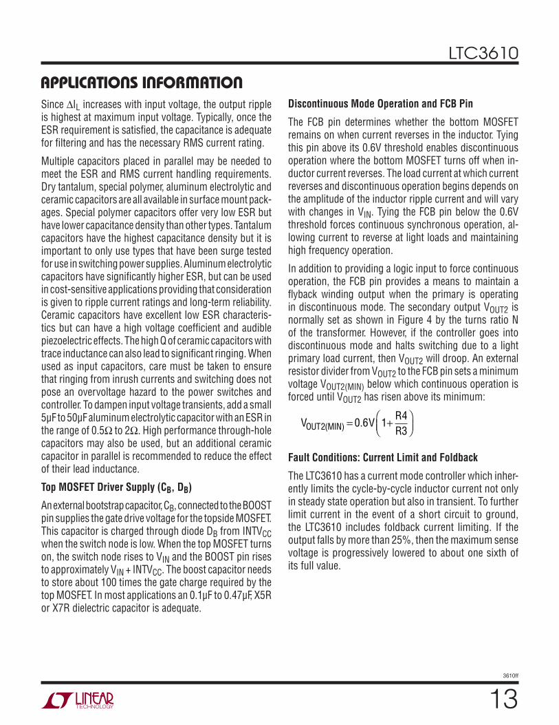
Multiple capacitors placed in parallel may be needed to meet the ESR and RMS current handling requirements. Dry tantalum, special polymer, aluminum electrolytic and ceramic capacitors are all available in surface mount pack-ages. Special polymer capacitors offer very low ESR but have lower capacitance density than other types. Tantalum capacitors have the highest capacitance density but it is important to only use types that have been surge tested for use in switching power supplies. Aluminum electrolytic capacitors have significantly higher ESR, but can be used in cost-sensitive applications providing that consideration is given to ripple current ratings and long-term reliability. Ceramic capacitors have excellent low ESR characteris-tics but can have a high voltage coefficient and audible piezoelectric effects. The high Q of ceramic capacitors with trace inductance can also lead to significant ringing. When used as input capacitors, care must be taken to ensure that ringing from inrush currents and switching does not pose an overvoltage hazard to the power switches and controller. To dampen input voltage transients, add a small 5µF to 50µF aluminum electrolytic capacitor with an ESR in the range of 0.5Ω to 2Ω. High performance through-hole capacitors may also be used, but an additional ceramic capacitor in parallel is recommended to reduce the effect of their lead inductance.
TopMOSFETDriverSupply(CB,DB)
An external bootstrap capacitor, CB, connected to the BOOST pin supplies the gate drive voltage for the topside MOSFET. This capacitor is charged through diode DB from INTVCC when the switch node is low. When the top MOSFET turns on, the switch node rises to VIN and the BOOST pin rises to approximately VIN + INTVCC. The boost capacitor needs to store about 100 times the gate charge required by the top MOSFET. In most applications an 0.1µF to 0.47µF, X5R or X7R dielectric capacitor is adequate.
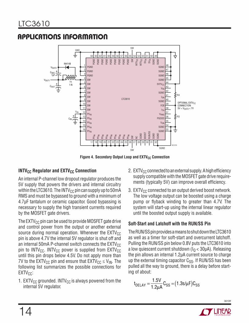
DiscontinuousModeOperationandFCBPin
The FCB pin determines whether the bottom MOSFET remains on when current reverses in the inductor. Tying this pin above its 0.6V threshold enables discontinuous operation where the bottom MOSFET turns off when in-ductor current reverses. The load current at which current reverses and discontinuous operation begins depends on the amplitude of the inductor ripple current and will vary with changes in VIN.Tying the FCB pin below the 0.6V threshold forces continuous synchronous operation, al-lowing current to reverse at light loads and maintaining high frequency operation.
In addition to providing a logic input to force continuous operation, the FCB pin provides a means to maintain a flyback winding output when the primary is operating in discontinuous mode. The secondary output VOUT2 is normally set as shown in Figure 4 by the turns ratio N of the transformer. However, if the controller goes into discontinuous mode and halts switching due to a light primary load current, then VOUT2 will droop. An external resistor divider from VOUT2 to the FCB pin sets a minimum voltage VOUT2(MIN) below which continuous operation is forced until VOUT2 has risen above its minimum:
VOUT2(MIN) = 0.6V 1+
R4R3
⎛⎝⎜
⎞⎠⎟
FaultConditions:CurrentLimitandFoldback
The LTC3610 has a current mode controller which inher-ently limits the cycle-by-cycle inductor current not only in steady state operation but also in transient. To further limit current in the event of a short circuit to ground, the LTC3610 includes foldback current limiting. If the output falls by more than 25%, then the maximum sense voltage is progressively lowered to about one sixth of its full value.
applications inForMation
LTC3610
��3610ff
applications inForMation
INTVCCRegulatorandEXTVCCConnection
An internal P-channel low dropout regulator produces the 5V supply that powers the drivers and internal circuitry within the LTC3610. The INTVCC pin can supply up to 50mA RMS and must be bypassed to ground with a minimum of 4.7µF tantalum or ceramic capacitor. Good bypassing is necessary to supply the high transient currents required by the MOSFET gate drivers.
The EXTVCC pin can be used to provide MOSFET gate drive and control power from the output or another external source during normal operation. Whenever the EXTVCC pin is above 4.7V the internal 5V regulator is shut off and an internal 50mA P-channel switch connects the EXTVCC pin to INTVCC. INTVCC power is supplied from EXTVCC until this pin drops below 4.5V. Do not apply more than 7V to the EXTVCC pin and ensure that EXTVCC ≤ VIN. The following list summarizes the possible connections for EXTVCC:
1. EXTVCC grounded. INTVCC is always powered from the internal 5V regulator.
2. EXTVCC connected to an external supply. A high efficiency supply compatible with the MOSFET gate drive require-ments (typically 5V) can improve overall efficiency.
3. EXTVCC connected to an output derived boost network. The low voltage output can be boosted using a charge pump or flyback winding to greater than 4.7V. The system will start-up using the internal linear regulator until the boosted output supply is available.
Soft-StartandLatchoffwiththeRUN/SSPin
The RUN/SS pin provides a means to shut down the LTC3610 as well as a timer for soft-start and overcurrent latchoff. Pulling the RUN/SS pin below 0.8V puts the LTC3610 into a low quiescent current shutdown (IQ < 30µA). Releasing the pin allows an internal 1.2µA current source to charge up the external timing capacitor CSS. If RUN/SS has been pulled all the way to ground, there is a delay before start-ing of about:
tDELAY =
1.5V1.2µA
CSS = 1.3s/µF( )CSS
Figure4.SecondaryOutputLoopandEXTVCCConnection
LTC3610
SGND48
SGND47
SGND46
SGND45
EXTVCC44
VFB43
SGND42
ION41 R4
SGND40
FCB39
ITH38
VRNG37
PGOOD36
VON35
SGND34
SGND
SGND
GND
33
PVIN
17
PVIN
18
PVIN
19
PVIN
20
PVIN
21
PVIN
22
PVIN
23
PVIN
24
PVIN
25
SW
SW
SW
26
NC
27SG
ND28
BOOS
T29
RUN/
SS
30
SGND
31
SGND
32
PGND
64
PGND
63
PGND
62
PGND
61
PGND
60
PGND
59
PGND
58
PGND
57
PGND
56
SW
55
INTV
CC
54
INTV
CC
53
SVIN
52
SVIN
51
SGND
50
SGND
49
PGND1
PGND2
PGND3
SW4
SW5
SW6
SW7
SW8
SW9
SW10
SW11
PVINVIN 12
PVIN13
PVIN14
PVIN15
PVIN16
3610 F04
CSEC1µF
VOUT2
VOUT1
COUT
CIN
IN4148
OPTIONAL EXTVCCCONNECTION5V < VOUT2 < 7V
T11:N
R3+
+
•
•
+

LTC3610
��3610ff
3.3V OR 5V RUN/SSVIN
INTVCC
RUN/SS
D1
(5a) (5b)
D2*
CSS
RSS*
CSS
*OPTIONAL TO OVERRIDE OVERCURRENT LATCHOFF
RSS*
3610 F05
2N7002
applications inForMation
Figure5.RUN/SSPinInterfacingwithLatchoffDefeated
When the voltage on RUN/SS reaches 1.5V, the LTC3610 begins operating with a clamp on ITH of approximately 0.9V. As the RUN/SS voltage rises to 3V, the clamp on ITH is raised until its full 2.4V range is available. This takes an additional 1.3s/µF, during which the load current is folded back until the output reaches 75% of its final value.
After the controller has been started and given adequate time to charge up the output capacitor, CSS is used as a short-circuit timer. After the RUN/SS pin charges above 4V, if the output voltage falls below 75% of its regulated value, then a short-circuit fault is assumed. A 1.8µA current then begins discharging CSS. If the fault condition persists until the RUN/SS pin drops to 3.5V, then the controller turns off both power MOSFETs, shutting down the converter permanently. The RUN/SS pin must be actively pulled down to ground in order to restart operation.
The overcurrent protection timer requires that the soft-start timing capacitor, CSS, be made large enough to guarantee that the output is in regulation by the time CSS has reached the 4V threshold. In general, this will depend upon the size of the output capacitance, output voltage and load current characteristic. A minimum soft-start capacitor can be estimated from:
CSS > COUT VOUT RSENSE (10 –4 [F/V s])
Generally 0.1µF is more than sufficient.
Overcurrent latchoff operation is not always needed or de-sired. Load current is already limited during a short-circuit by the current foldback circuitry and latchoff operation can prove annoying during troubleshooting. The feature can be overridden by adding a pull-up current greater than 5µA to the RUN/SS pin. The additional current prevents the discharge of CSS during a fault and also shortens the soft-start period. Using a resistor to VIN as shown in Fig-ure 5a is simple, but slightly increases shutdown current. Connecting a resistor to INTVCC as shown in Figure 5b eliminates the additional shutdown current, but requires a diode to isolate CSS. Any pull-up network must be able to pull RUN/SS above the 4.2V maximum threshold of the latchoff circuit and overcome the 4µA maximum discharge current.
EfficiencyConsiderations
The percent efficiency of a switching regulator is equal to the output power divided by the input power times 100%. It is often useful to analyze individual losses to determine what is limiting the efficiency and which change would produce the most improvement. Although all dissipative elements in the circuit produce losses, four main sources account for most of the losses in LTC3610 circuits:
1. DC I2R losses. These arise from the resistance of the internal resistance of the MOSFETs, inductor and PC board traces and cause the efficiency to drop at high output currents. In continuous mode the average output current flows through L, but is chopped between the top and bottom MOSFETs. The DC I2R loss for one MOSFET can simply be determined by [RDS(ON) + RL] • IO.
2. Transition loss. This loss arises from the brief amount of time the top MOSFET spends in the saturated re-gion during switch node transitions. It depends upon the input voltage, load current, driver strength and MOSFET capacitance, among other factors. The loss is significant at input voltages above 20V and can be estimated from:
Transition Loss ≅ (1.7A–1) VIN2 IOUT CRSS f
3. INTVCC current. This is the sum of the MOSFET driver and control currents. This loss can be reduced by sup-plying INTVCC current through the EXTVCC pin from a high efficiency source, such as an output derived boost network or alternate supply if available.

LTC3610
��3610ff
applications inForMation4. CIN loss. The input capacitor has the difficult job of filtering
the large RMS input current to the regulator. It must have a very low ESR to minimize the AC I2R loss and sufficient capacitance to prevent the RMS current from causing additional upstream losses in fuses or batteries.
Other losses, including COUT ESR loss, Schottky diode D1 conduction loss during dead time and inductor core loss generally account for less than 2% additional loss.
When making adjustments to improve efficiency, the input current is the best indicator of changes in efficiency. If you make a change and the input current decreases, then the efficiency has increased. If there is no change in input current, then there is no change in efficiency.
CheckingTransientResponse
The regulator loop response can be checked by looking at the load transient response. Switching regulators take several cycles to respond to a step in load current. When a load step occurs, VOUT immediately shifts by an amount equal to ΔILOAD (ESR), where ESR is the effective series resistance of COUT. ΔILOAD also begins to charge or dis-charge COUT generating a feedback error signal used by the regulator to return VOUT to its steady-state value. During this recovery time, VOUT can be monitored for overshoot or ringing that would indicate a stability problem. The ITH pin external components shown in Figure 6 will provide adequate compensation for most applications. For a detailed explanation of switching control loop theory see Application Note 76.
DesignExample
As a design example, take a supply with the following specifications: VIN = 5V to 24V (12V nominal), VOUT = 2.5V ±5%, IOUT(MAX) = 12A, f = 550kHz. First, calculate the timing resistor with VON = VOUT:
R
kHz pFkON = ( )( ) =
1550 10
182
and choose the inductor for about 40% ripple current at the maximum VIN:
L =2.5V
550kHz( ) 0.4( ) 12A( )1−
2.5V28V
⎛⎝⎜
⎞⎠⎟= 0.86µH
Selecting a standard value of 0.82µH results in a maximum ripple current of:
ΔIL =
2.5V550kHz( ) 0.82µH( )
1–2.5V12V
⎛⎝⎜
⎞⎠⎟= 4.4A
Next, set up VRNG voltage and check the ILIMIT. Tying VRNG to 0.5V will set the typical current limit to 16A, and tying VRNG to GND will result in a typical current around 19A.CIN is chosen for an RMS current rating of about 5A at 85°C. The output capacitors are chosen for a low ESR of 0.013Ω to minimize output voltage changes due to inductor ripple current and load steps. The ripple voltage will be only:
ΔVOUT(RIPPLE) = ΔIL(MAX) (ESR) = (4.4A) (0.013Ω) = 57mV
However, a 0A to 10A load step will cause an output change of up to:
ΔVOUT(STEP) = ΔILOAD (ESR) = (10A) (0.013Ω) = 130mV
An optional 22µF ceramic output capacitor is included to minimize the effect of ESL in the output ripple. The complete circuit is shown in Figure 6.
How to Reduce SW Ringing
As with any switching regulator, there will be voltage ring-ing on the SW node, especially for high input voltages. The ringing amplitude and duration is dependent on the switching speed (gate drive), layout (parasitic inductance) and MOSFET output capacitance. This ringing contributes to the overall EMI, noise and high frequency ripple. One way to reduce ringing is to optimize layout. A good layout minimizes parasitic inductance. Adding RC snubbers from SW to GND is also an effective way to reduce ringing. Finally, adding a resistor in series with the BOOST pin will slow down the MOSFET turn-on slew rate to dampen ringing, but at the cost of reduced efficiency. Note that since the IC is buffered from the high frequency transients by PCB and bondwire inductances, the ringing by itself is normally not a concern for controller reliability.
LTC3610
��3610ff
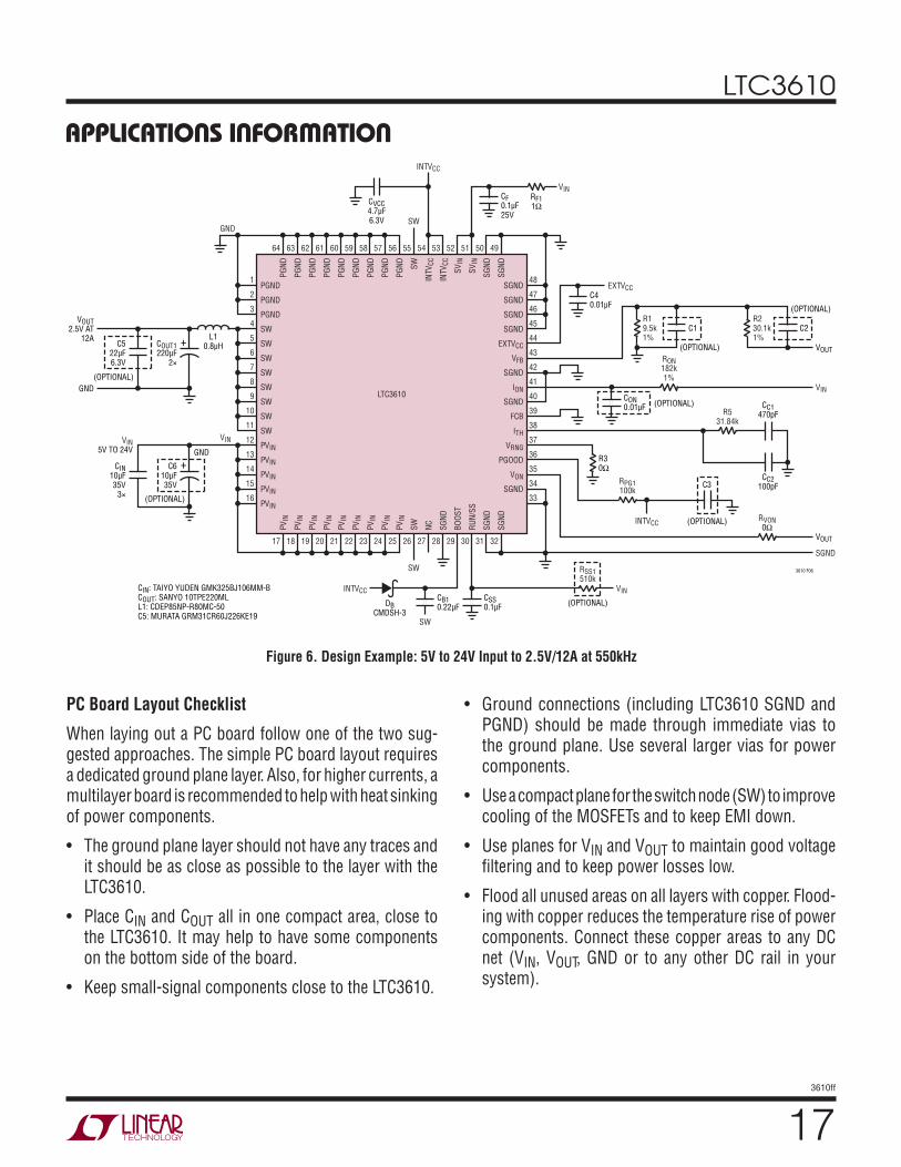
Figure6.DesignExample:5Vto24VInputto2.5V/12Aat550kHz
VOUT2.5V AT
12A
GND
GND
VINVIN5V TO 24V
COUT1220µF
2×
C522µF6.3V
L10.8µH
CIN10µF35V
3×
+
C610µF35V
+
(OPTIONAL)
(OPTIONAL)
CIN: TAIYO YUDEN GMK325BJ106MM-BCOUT: SANYO 10TPE220MLL1: CDEP85NP-R80MC-50C5: MURATA GRM31CR60J226KE19
LTC3610
SGND48
SGND47
SGND46
SGND45
EXTVCC
EXTVCC
44
VFB43
SGND42
ION41
SGND40
FCB39
ITH38
VRNG37
PGOOD36
VON35
SGND34
SGND
GND
VOUT
VOUT
33
PVIN
17
PVIN
18
PVIN
19
PVIN
20
PVIN
21
PVIN
22
PVIN
23
PVIN
24
PVIN
25
SW
SW
SW
SW
26
NC
27
SGND
28
BOOS
T
29
RUN/
SS
30
SGND
31
SGND
32
PGND
64
PGND
63
PGND
62
PGND
61
PGND
60
PGND
59
PGND
58
PGND
57
PGND
56
SW
55
INTV
CC
INTVCC
INTVCC
54
INTV
CC
INTVCC
53
SVIN
VIN
52
SVIN
51
SGND
50
SGND
49
PGND1
PGND2
PGND3
SW4
SW5
SW6
SW7
SW8
SW9
SW10
SW11
PVIN
VIN
12
PVIN13
PVIN14
PVIN15
PVIN16
3610 F06
CF0.1µF25V
RF11ΩCVCC
4.7µF6.3V
C3
CON0.01µF
C40.01µF
C2C1
CB10.22µFDB
CMDSH-3
CSS0.1µF
VIN
RSS1510k
(OPTIONAL)
(OPTIONAL)
(OPTIONAL)
(OPTIONAL)
R19.5k1%
R230.1k1%
RVON0Ω
RPG1100k
RON182k1%
R531.84k
R30Ω
CC1470pF
CC2100pF
(OPTIONAL)
applications inForMation
PCBoardLayoutChecklist
When laying out a PC board follow one of the two sug-gested approaches. The simple PC board layout requires a dedicated ground plane layer. Also, for higher currents, a multilayer board is recommended to help with heat sinking of power components.
• The ground plane layer should not have any traces and it should be as close as possible to the layer with the LTC3610.
• Place CIN and COUT all in one compact area, close to the LTC3610. It may help to have some components on the bottom side of the board.
• Keep small-signal components close to the LTC3610.
• Ground connections (including LTC3610 SGND and PGND) should be made through immediate vias to the ground plane. Use several larger vias for power components.
• Use a compact plane for the switch node (SW) to improve cooling of the MOSFETs and to keep EMI down.
• Use planes for VIN and VOUT to maintain good voltage filtering and to keep power losses low.
• Flood all unused areas on all layers with copper. Flood-ing with copper reduces the temperature rise of power components. Connect these copper areas to any DC net (VIN, VOUT, GND or to any other DC rail in your system).

LTC3610
��3610ff
Figure7.LTC3610LayoutDiagram
LTC3610
SGND48
SGND47
SGND46
SGND45
EXTVCC44
VFB43
SGND42
ION41
SGND40
FCB39
ITH38
VRNG37
PGOOD36
VON35
SGND34
33
PVIN
17
PVIN
18
PVIN
19
PVIN
20
PVIN
21
PVIN
22
PVIN
23
PVIN
24
PVIN
25
SW
26
NC
27
SGND
28
BOOS
T
29
RUN/
SS
30
SGND
31
SGND
32
PGND
64
PGND
63
PGND
62
PGND
61
PGND
60
PGND
59
PGND
58
PGND
57
PGND
56
SW
SW
55
INTV
CC
54
INTV
CC
53
SVIN
52
SVIN
51
SGND
50
SGND
49
PGND1
PGND2
PGND3
SW4
SW5
SW6
SW7
SW8
SW9
SW10
SW11
PVIN12
PVIN13
PVIN14
PVIN15
PVIN16
3610 F07
CIN
COUT
VOUT
CVCC
CBDB CSS
R1
RF
RON
R2
RCCC1
CC2
applications inForMation
When laying out a printed circuit board without a ground plane, use the following checklist to ensure proper opera-tion of the controller. These items are also illustrated in Figure 7.
• Segregate the signal and power grounds. All small-signal components should return to the SGND pin at one point, which is then tied to the PGND pin.
• Connect the input capacitor(s), CIN, close to the IC. This capacitor carries the MOSFET AC current.
• Keep the high dV/dT SW, BOOST and TG nodes away from sensitive small-signal nodes.
• Connect the INTVCC decoupling capacitor, CVCC, closely to the INTVCC and PGND pins.
• Connect the top driver boost capacitor, CB, closely to the BOOST and SW pins.
• Connect the VIN pin decoupling capacitor, CF, closely to the VIN and PGND pins.
LTC3610
��3610ff
typical applications
LTC3610
SGND48
SGND47
SGND46
SGND45
EXTVCC
EXTVCC
44
VFB43
SGND42
ION41
SGND40
FCB39
ITH38
VRNG37
PGOOD36
VON35
SGND34
SGND
GND
VOUT1.5V AT
12A
VOUT
VOUT
GND
GND
33
PVIN
17
PVIN
18
PVIN
19
PVIN
20
PVIN
21
PVIN
22
PVIN
23
PVIN
24
PVIN
25
SW
SW
26
NC
27
SGND
28
BOOS
T
29
RUN/
SS
30
SGND
31
SGND
32
PGND
64
PGND
63
PGND
62
PGND
61
PGND
60
PGND
59
PGND
58
PGND
57
PGND
56
SW
55
INTV
CC
INTVCC
INTVCC
54
INTV
CC
INTVCC
53
SVIN
VIN2 = 5V
52
SVIN
51
SGND
50
SGND
49
PGND1
PGND2
PGND3
SW4
SW5
SW6
SW7
SW8
SW9
SW10
SW11
PVIN
VIN
VIN 12
PVIN13
PVIN14
PVIN15
PVIN16
3610 TA02
COUT1220µF
2×
C522µF6.3V
L10.36µH
CF0.1µF25V
CIN10µF
3×
CVCC4.7µF6.3V
+
C610µF35V
+
(OPTIONAL)
(OPTIONAL)
CIN: TAIYO YUDEN TMK432BJ106MMCOUT1: SANYO 10TPE220MLL1: TOKO FDH1040-36MC5: TAIYO YUDEN JMK316BJ226ML-T
CVON
CON0.01µF
C40.01µF
C2C1
CB10.22µF
CSS0.1µF
VIN
RSS1510k
(OPTIONAL)
(OPTIONAL)
(OPTIONAL)
(OPTIONAL)
(OPTIONAL)
(OPTIONAL)
R120.43k1%
R230.1k1%
RVON
RPG1100k
RON113k1%
R511.15k
CC1470pF
CC2100pF
VIN3.3V
3.3VInputto1.5V/12Aat750kHz

LTC3610
�03610ff
5Vto24VInputto1.2V/12Aat550kHz
typical applications
VOUT1.2V AT
12A
GND
GND
VIN
COUT1220µF
2×
C522µF6.3V
L10.52µH
CIN10µF25V
3×
+
C610µF35V
+
(OPTIONAL)
(OPTIONAL)
C5: TAIYO YUDEN JMK316BJ226ML-TCIN: TAIYO YUDEN TMK432BJ106MMCOUT1: SANYO 10TPE220MLL1: WURTH 744310055
LTC3610
SGND48
SGND47
SGND46
SGND45
EXTVCC
EXTVCC
44
VFB43
SGND42
ION41
SGND40
FCB39
ITH38
VRNG37
PGOOD36
VON35
SGND34
SGNDSGND
GND
VOUT
VOUT
33
PVIN
17
PVIN
18
PVIN
19
PVIN
20
PVIN
21
PVIN
22
PVIN
23
PVIN
24
PVIN
25
SW
26
NC
27
SGND
28 29
RUN/
SS
30
SGND
31
SGND
32
PGND
64
PGND
63
PGND
62
PGND
61
PGND
60
PGND
59
PGND
58
PGND
57
PGND
56
SW
55
INTV
CC
INTVCC
54
INTV
CC
INTVCC
53
SVIN
VIN
52
SVIN
51
SGND
50
SGND
49
PGND1
PGND2
PGND3
SW4
SW5
SW6
SW7
SW8
SW9
SW10
SW11
PVIN
VIN
12
PVIN13
PVIN14
PVIN15
PVIN16
3610 TA03
CF0.1µF25V
RF11ΩCVCC
4.7µF6.3V
CON0.01µF
C40.01µF
C2C1
DBCMDSH-3
CSS0.1µF
VIN
RSS1510k
(OPTIONAL)
(OPTIONAL)
(OPTIONAL)
(OPTIONAL)R130k1%
R230.1k1%
RPG1100k
RON301k1%
R531.84k
CC1470pF
CC2100pF
CVON(OPTIONAL)
RVON
VIN5V TO 24V
SW BOOS
T
INTVCC
CB10.22µF

LTC3610
��3610ff
typical applications5Vto24VInputto1.8V/12AAllCeramic1MHz
VOUT1.8V AT
12A
GND
VINVIN5V TO 24V
COUT100µF
2×
C522µF6.3V
L10.47µH
CIN10µF25V
3×
(OPTIONAL)
COUT: TAIYO YUDEN JMK325BJ107MYL1: TOKIN MPLC0730C5: TAIYO YUDEN JMK316BJ226ML-T
LTC3610
SGND48
SGND47
SGND46
SGND45
EXTVCC
EXTVCC
44
VFB43
SGND42
ION41
SGND40
FCB39
ITH38
VRNG37
PGOOD36
VON35
SGND34
SGND
GND
VOUT
VOUT
33
PVIN
17
PVIN
18
PVIN
19
PVIN
20
PVIN
21
PVIN
22
PVIN
23
PVIN
24
PVIN
25
SW
26
NC
27
SGND
28 29
RUN/
SS
30
SGND
31
SGND
32
PGND
64PG
ND63
PGND
62
PGND
61
PGND
60
PGND
59
PGND
58
PGND
57
PGND
56
SW
55
INTV
CC
INTVCC
54
INTV
CC
INTVCC
53
SVIN
VIN
52
SVIN
51
SGND
50
SGND
49
PGND1
PGND2
PGND3
SW4
SW5
SW6
SW7
SW8
SW9
SW10
SW11
PVIN
VIN
12
PVIN13
PVIN14
PVIN15
PVIN16
3610 TA04
CF0.1µF25V
RF11ΩCVCC
4.7µF6.3V
CON0.01µF
C40.01µF
C2C1
DBCMDSH-3
CSS0.1µF
VIN
RSS1510k
(OPTIONAL)
(OPTIONAL)
(OPTIONAL)
(OPTIONAL)R110k1%
R220k1%
RPG1100k
RON102k1%
R518.7k
CC1560pF
CC2100pF
CVON(OPTIONAL)
(OPTIONAL)
RVONSW BOOS
T
INTVCC
CB10.22µF

LTC3610
��3610ff
package Description
WP
Pack
age
64-L
ead
QFN
Mul
tipad
(9m
m×
9m
m)
(Ref
eren
ce LT
C DW
G #
05-0
8-18
12 R
ev A
)
9.00
BSC
9.00
BSC
17
16
32
33
BOTT
OM V
IEW
(BOT
TOM
MET
ALLI
ZATI
ON D
ETAI
LS)
TOP
VIEW
0.90
± 0
.10
// c
cc C0.
20 R
EF
0.00
– 0
.05
0.30
– 0
.50
WP6
4 QF
N RE
V A
0707
0.20
– 0
.30
NX b
SEAT
ING
PLAN
E 65 0.08
C
aaa
C
aaa C
MA CB bbb
NX
A
B
2x
2x
3.30
1.19
49
48
5051
5253
5464
1
1.39
1.17
0.53
(2x)
1.92
2.01
3.06
4.10
3.30
0.30
(2x) 0.
95
3.50
0.87
3.60
0.50
1.81
2.04
2.98
3.99
4.53
NOTE
:1.
DIM
ENSI
ONIN
G AN
D TO
LERA
NCIN
G CO
NFOR
M T
O AS
ME
Y14.
5M-1
994
2. A
LL D
IMEN
SION
S AR
E IN
MIL
LIM
ETER
S, A
NGLE
S AR
E IN
DEG
REES
(°)
3. N
IS T
HE T
OTAL
NUM
BER
OF T
ERM
INAL
S4.
THE
LOC
ATIO
N OF
THE
TER
MIN
AL #
1 ID
ENTI
FIER
AND
TER
MIN
AL N
UMBE
RING
CON
VENT
ION
CONF
ORM
S TO
JED
EC P
UBLI
CATI
ON 9
5 SP
P-00
2
6CO
PLAN
ARIT
Y AP
PLIE
S TO
THE
TER
MIN
ALS
AND
ALL
OTHE
R SU
RFAC
E M
ETAL
LIZA
TION
5DI
MEN
SION
b A
PPLI
ES T
O M
ETAL
LIZE
D TE
RMIN
AL A
ND IS
MEA
SURE
D BE
TWEE
N 0.
15m
m A
ND 0
.30m
m F
ROM
THE
TER
MIN
AL T
IP.
SYM
BOL
aaa
bbb
ccc
TOLE
RANC
E0.
150.
100.
10
WP
Pack
age
64-L
ead
QFN
Mul
tipad
(9m
m ×
9m
m)
(Ref
eren
ce L
TC D
WG
# 05
-08-
1812
Rev
A)
3.85
1.42
PAD
1CO
RNER
RECO
MM
ENDE
D SO
LDER
PAD
LAY
OUT
TOP
VIEW
0.30
– 0
.50
3.30
1.19
1.17
1.92
2.01
3.06
4.10
0.53
(2x)
1.39
3.30
0.30
(2x)
2.30
3.50
0.87
3.60
PIN
1
0.50
1.81
2.04
2.98
3.994.
53
0.20
– 0
.30
3.85
1.42
0.95
1.30
1.30

LTC3610
��3610ff
Information furnished by Linear Technology Corporation is believed to be accurate and reliable. However, no responsibility is assumed for its use. Linear Technology Corporation makes no representa-tion that the interconnection of its circuits as described herein will not infringe on existing patent rights.
revision historyREV DATE DESCRIPTION PAGE NUMBER
F 07/10 I-grade part added. Reflected throughout the data sheet. 1 to 24
(Revision history begins at Rev F)
LTC3610
��3610ff
Linear Technology Corporation1630 McCarthy Blvd., Milpitas, CA 95035-7417 (408) 432-1900 ● FAX: (408) 434-0507 ● www.linear.com LINEAR TECHNOLOGY CORPORATION 2007
LT 0710 REV F • PRINTED IN USA
VOUT12V AT
5A
GND
GND
VINVIN14V TO 24V
COUT180µF
16V
C522µF25V
L15.7µH
CIN10µF25V
3×
+
C610µF35V
+
(OPTIONAL)
(OPTIONAL)
CIN: TAIYO YUDEN TMK432BJ106MMCOUT: SANYO 16SVP180MXL1: SUMIDA CDEP1055R7
LTC3610
SGND48
SGND47
SGND46
SGND45
EXTVCC
EXTVCC
44
VFB43
SGND42
ION41
SGND40
FCB39
ITH38
VRNG37
PGOOD36
VON35
SGND34
SGND
GND
INTVCC
VOUT
33
PVIN
17
PVIN
18
PVIN
19
PVIN
20
PVIN
21
PVIN
22
PVIN
23
PVIN
24
PVIN
25
SW
26 27
SGND
28 29
RUN/
SS
30
SGND
31
SGND
32
PGND
64
PGND
63
PGND
62
PGND
61
PGND
60
PGND
59
PGND
58
PGND
57
PGND
56
SW
55
INTV
CC
INTVCC
54
INTV
CC
INTVCC
53
SVIN
VIN
52
SVIN
51
SGND
50
SGND
49
PGND1
PGND2
PGND3
SW4
SW5
SW6
SW7
SW8
SW9
SW10
SW11
PVIN
VIN
12
PVIN13
PVIN14
PVIN15
PVIN16
3610 TA05
CF0.1µF25V
RF11Ω
CVCC4.7µF6.3V
CON0.01µF
C40.01µF
C2C1
RUN/SS
CSS0.1µF
VIN
RSS1510k
(OPTIONAL)
(OPTIONAL)
(OPTIONAL)
R11.58k1%
R230.1k1%
RPG1100k
RON1M1%
R520k
CC1560pF
CC2100pF
(OPTIONAL)
CVON(OPTIONAL)
(OPTIONAL)
RVONNC
DBCMDSH-3
SW BOOS
T
INTVCC
CB10.22µF
relateD parts
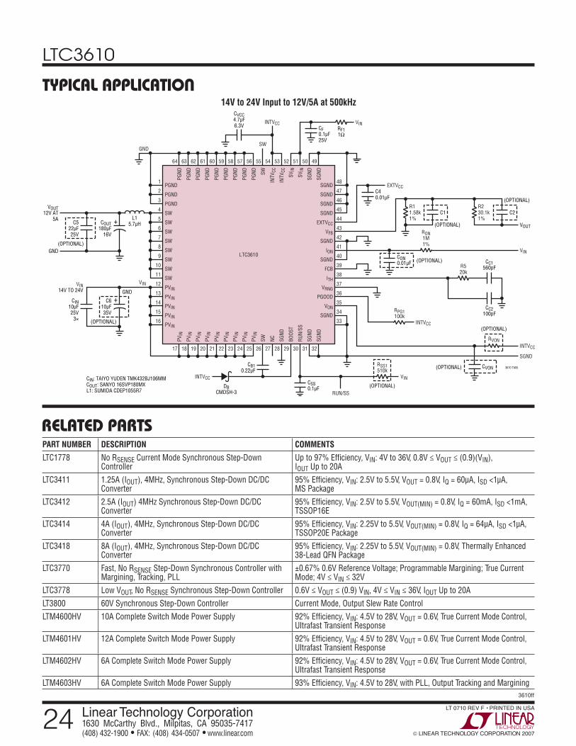
typical application14Vto24VInputto12V/5Aat500kHz
PARTNUMBER DESCRIPTION COMMENTSLTC1778 No RSENSE Current Mode Synchronous Step-Down
ControllerUp to 97% Efficiency, VIN: 4V to 36V, 0.8V ≤ VOUT ≤ (0.9)(VIN), IOUT Up to 20A
LTC3411 1.25A (IOUT), 4MHz, Synchronous Step-Down DC/DC Converter
95% Efficiency, VIN: 2.5V to 5.5V, VOUT = 0.8V, IQ = 60µA, ISD <1µA, MS Package
LTC3412 2.5A (IOUT) 4MHz Synchronous Step-Down DC/DC Converter
95% Efficiency, VIN: 2.5V to 5.5V, VOUT(MIN) = 0.8V, IQ = 60mA, ISD <1mA, TSSOP16E
LTC3414 4A (IOUT), 4MHz, Synchronous Step-Down DC/DC Converter
95% Efficiency, VIN: 2.25V to 5.5V, VOUT(MIN) = 0.8V, IQ = 64µA, ISD <1µA, TSSOP20E Package
LTC3418 8A (IOUT), 4MHz, Synchronous Step-Down DC/DC Converter
95% Efficiency, VIN: 2.25V to 5.5V, VOUT(MIN) = 0.8V, Thermally Enhanced 38-Lead QFN Package
LTC3770 Fast, No RSENSE Step-Down Synchronous Controller with Margining, Tracking, PLL
±0.67% 0.6V Reference Voltage; Programmable Margining; True Current Mode; 4V ≤ VIN ≤ 32V
LTC3778 Low VOUT, No RSENSE Synchronous Step-Down Controller 0.6V ≤ VOUT ≤ (0.9) VIN, 4V ≤ VIN ≤ 36V, IOUT Up to 20A
LT3800 60V Synchronous Step-Down Controller Current Mode, Output Slew Rate Control
LTM4600HV 10A Complete Switch Mode Power Supply 92% Efficiency, VIN: 4.5V to 28V, VOUT = 0.6V, True Current Mode Control, Ultrafast Transient Response
LTM4601HV 12A Complete Switch Mode Power Supply 92% Efficiency, VIN: 4.5V to 28V, VOUT = 0.6V, True Current Mode Control, Ultrafast Transient Response
LTM4602HV 6A Complete Switch Mode Power Supply 92% Efficiency, VIN: 4.5V to 28V, VOUT = 0.6V, True Current Mode Control, Ultrafast Transient Response
LTM4603HV 6A Complete Switch Mode Power Supply 93% Efficiency, VIN: 4.5V to 28V, with PLL, Output Tracking and Margining