Embed Size (px)
Citation preview

LTC2508-32
1250832fc
For more information www.linear.com/LTC2508-32
TYPICAL APPLICATION
FEATURES DESCRIPTION
32-Bit Oversampling ADC with Configurable Digital Filter
The LTC®2508-32 is a low noise, low power, high perfor-mance 32-bit ADC with an integrated configurable digital filter. Operating from a single 2.5V supply, the LTC2508-32 features a fully differential input range up to ±VREF, with VREF ranging from 2.5V to 5.1V. The LTC2508-32 supports a wide common mode range from 0V to VREF simplifying analog signal conditioning requirements.
The LTC2508-32 simultaneously provides two output codes: (1) a 32-bit digitally filtered high precision low noise code, and (2) a 22-bit no latency composite code. The configurable digital filter reduces measurement noise by lowpass filtering and down-sampling the stream of data from the SAR ADC core, giving the 32-bit filtered output code. The 22-bit composite code consists of a 14-bit code representing the differential voltage and an 8-bit code representing the common mode voltage. The 22-bit composite code is available each conversion cycle, with no cycle of latency.
The digital filter can be easily configured for 4 different down-sampling factors by pin strapping. The configura-tions provide a dynamic range of 131dB at 3.9ksps and 145dB at 61sps. The digital lowpass filter relaxes the re-quirements for analog anti-aliasing. Multiple LTC2508-32 devices can be easily synchronized using the SYNC pin.
APPLICATIONS
n ±0.5ppm INL (Typ) n 145dB Dynamic Range (Typ) at 61sps n 131dB Dynamic Range (Typ) at 4ksps n Guaranteed 32-Bits No Missing Codes n Configurable Digital Filter with Synchronization
n Relaxed Anti-Aliasing Filter Requirements n Dual Output 32-Bit SAR ADC
n 32-Bit Digitally Filtered Low Noise Output n 14-Bit Differential + 8-Bit Common Mode 1Msps
No Latency Output n Wide Input Common Mode Range n Guaranteed Operation to 85°C n 1.8V to 5V SPI-Compatible Serial I/O n Low Power: 24mW at 1Msps n 24-Lead 7mm × 4mm DFN Package
n Seismology n Energy Exploration n Automated Test Equipment (ATE) n High Accuracy Instrumentation
L, LT, LTC, LTM, Linear Technology and the Linear logo are registered trademarks and SoftSpan is a trademark of Analog Devices, Inc. All other trademarks are the property of their respective owners. Protected by U.S. Patents, including 7705765, 7961132, 8319673, 8576104, 8810443, 9054727, 9231611, 9331709 and patents pending.
2.5V
IN+
IN–
DIFFERENTIAL
DIFFERENTIAL INPUTS IN+/IN– WITHWIDE INPUT COMMON MODE RANGE
ARBITRARY
UNIPOLARBIPOLAR
REF GND
LTC2508-32
RDLA
DRL
RDLB
SDOASCKA
SCKBSDOB
BUSYMCLKVDD
VREF
0V 0V
VREF
VREF
0V 0V
VREF
OVDD
10µF 0.1µF
1.8V TO 5.1V
2.5V TO 5.1V
SAMPLECLOCK
250832 TA01
47µF(X7R, 1210 SIZE)
IN+, IN–
32-BITSAR ADC
CORE
32-BIT
14-BIT
PIN SELECTABLE LOW-PASS WIDEBAND
DIGITAL FILTER
Integral Nonlinearity vs Input Voltage
INPUT VOLTAGE (V)250832 TA01a
–5 –2.5 0 2.5 5–2.0
–1.5
–1.0
–0.5
0
0.5
1.0
1.5
2.0
INL
ERRO
R (p
pm)
LTC2508-32
2250832fc
For more information www.linear.com/LTC2508-32
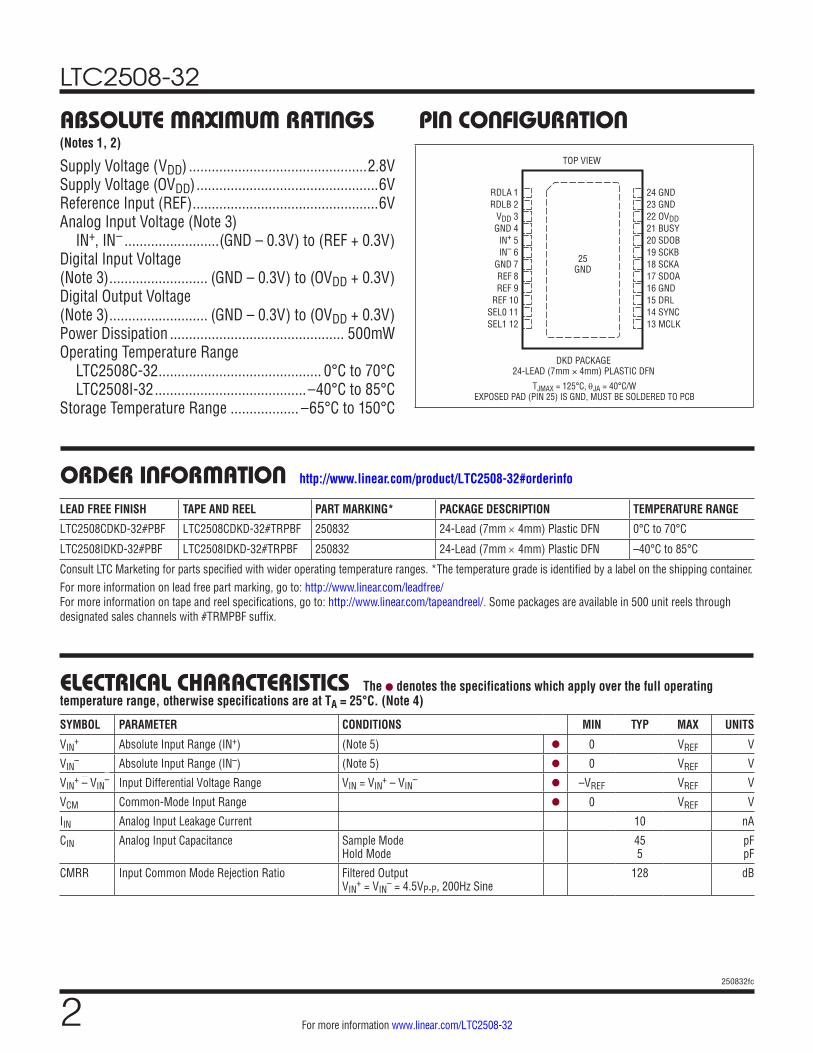
PIN CONFIGURATIONABSOLUTE MAXIMUM RATINGS
Supply Voltage (VDD) ...............................................2.8VSupply Voltage (OVDD) ................................................6VReference Input (REF) .................................................6VAnalog Input Voltage (Note 3) IN+, IN– .........................(GND – 0.3V) to (REF + 0.3V)Digital Input Voltage(Note 3) .......................... (GND – 0.3V) to (OVDD + 0.3V)Digital Output Voltage(Note 3) .......................... (GND – 0.3V) to (OVDD + 0.3V)Power Dissipation .............................................. 500mWOperating Temperature Range LTC2508C-32 ........................................... 0°C to 70°C LTC2508I-32 ........................................–40°C to 85°CStorage Temperature Range .................. –65°C to 150°C
(Notes 1, 2)TOP VIEW
25GND
DKD PACKAGE24-LEAD (7mm × 4mm) PLASTIC DFN
RDLA 1RDLB 2
VDD 3GND 4
IN+ 5IN– 6
GND 7REF 8REF 9
REF 10 SEL0 11SEL1 12
24 GND 23 GND22 OVDD21 BUSY20 SDOB19 SCKB18 SCKA17 SDOA16 GND15 DRL14 SYNC13 MCLK
TJMAX = 125°C, θJA = 40°C/W
EXPOSED PAD (PIN 25) IS GND, MUST BE SOLDERED TO PCB
ORDER INFORMATION
ELECTRICAL CHARACTERISTICS
SYMBOL PARAMETER CONDITIONS MIN TYP MAX UNITS
VIN+ Absolute Input Range (IN+) (Note 5) l 0 VREF V
VIN– Absolute Input Range (IN–) (Note 5) l 0 VREF V
VIN+ – VIN
– Input Differential Voltage Range VIN = VIN+ – VIN
– l –VREF VREF V
VCM Common-Mode Input Range l 0 VREF V
IIN Analog Input Leakage Current 10 nA
CIN Analog Input Capacitance Sample Mode Hold Mode
45 5
pF pF
CMRR Input Common Mode Rejection Ratio Filtered Output VIN
+ = VIN– = 4.5VP-P, 200Hz Sine
128 dB
The l denotes the specifications which apply over the full operating temperature range, otherwise specifications are at TA = 25°C. (Note 4)
LEAD FREE FINISH TAPE AND REEL PART MARKING* PACKAGE DESCRIPTION TEMPERATURE RANGE
LTC2508CDKD-32#PBF LTC2508CDKD-32#TRPBF 250832 24-Lead (7mm × 4mm) Plastic DFN 0°C to 70°C
LTC2508IDKD-32#PBF LTC2508IDKD-32#TRPBF 250832 24-Lead (7mm × 4mm) Plastic DFN –40°C to 85°C
Consult LTC Marketing for parts specified with wider operating temperature ranges. *The temperature grade is identified by a label on the shipping container.For more information on lead free part marking, go to: http://www.linear.com/leadfree/ For more information on tape and reel specifications, go to: http://www.linear.com/tapeandreel/. Some packages are available in 500 unit reels through designated sales channels with #TRMPBF suffix.
http://www.linear.com/product/LTC2508-32#orderinfo

LTC2508-32
3250832fc
For more information www.linear.com/LTC2508-32
DYNAMIC ACCURACY FOR FILTERED OUTPUT (SDOA)
CONVERTER CHARACTERISTICS FOR FILTERED OUTPUT (SDOA)
SYMBOL PARAMETER CONDITIONS MIN TYP MAX UNITS
DR Dynamic Range VREF = 5V, DF = 256 IN+ = IN– = VCM, VREF = 5V, DF = 1024 IN+ = IN– = VCM, VREF = 5V, DF = 4096 IN+ = IN– = VCM, VREF = 5V, DF = 16384
l 125 131 136 141 145
dB dB dB dB
THD Total Harmonic Distortion fIN = 200Hz, VREF = 2.5V, DF = 256 fIN = 200Hz, VREF = 5V, DF = 256
l
–118 –118
–108
dB dB
SFDR Spurious Free Dynamic Range fIN = 200Hz, VREF = 2.5V, DF = 256 fIN = 200Hz, VREF = 5V, DF = 256
l
108
118 118
dB dB
–3dB Input Bandwidth 34 MHz
Aperture Delay 500 ps
Aperture Jitter 4 psRMS
Transient Response Full-Scale Step 125 ns
SYMBOL PARAMETER CONDITIONS MIN TYP MAX UNITS
Resolution l 32 Bits
No Missing Codes l 32 Bits
DF Down-sampling Factor l 256 16384
Transition Noise DF = 256 (Note 6) DF = 1024 DF = 4096 DF = 16384
0.095 0.055 0.03 0.02
ppm ppm ppm ppm
INL Integral Linearity Error (Note 7) l –3.5 0.5 3.5 ppm
ZSE Zero-Scale Error (Note 9) l –13 0 13 ppm
Zero-Scale Error Drift ±14 ppb/°C
FSE Full-Scale Error (Note 9) l –100 ±10 100 ppm
Full-Scale Error Drift ±0.05 ppm/°C
The l denotes the specifications which apply over the full operating temperature range, otherwise specifications are at TA = 25°C and AIN = –20dBFS. (Notes 4, 10)
The l denotes the specifications which apply over the full operating temperature range, otherwise specifications are at TA = 25°C. (Note 4)

LTC2508-32
4250832fc
For more information www.linear.com/LTC2508-32
CONVERTER CHARACTERISTICS FOR NO LATENCY OUTPUT (SDOB)
REFERENCE INPUT
DIGITAL INPUTS AND DIGITAL OUTPUTS
SYMBOL PARAMETER CONDITIONS MIN TYP MAX UNITS
Resolution: Differential Common Mode
l
l
14 8
Bits Bits
No Missing Codes: Differential Common Mode
l
l
14 8
Bits Bits
Transition Noise Differential Common Mode
(Note 6) 1 1
LSBRMS LSBRMS
INL Integral Linearity Error Differential Common Mode
(Note 7) ±0.1 ±0.1
LSB LSB
DNL Differential Linearity Error Differential Common Mode
±0.1 ±0.1
LSB LSB
ZSE Zero Scale Error Differential Common Mode
±1 ±1
LSB LSB
FSE Zero Scale Error Differential Common Mode
±1 ±1
LSB LSB
SYMBOL PARAMETER CONDITIONS MIN TYP MAX UNITS
VREF Reference Voltage (Note 5) l 2.5 5.1 V
IREF Reference Input Current (Note 11) l 0.7 1 mA
SYMBOL PARAMETER CONDITIONS MIN TYP MAX UNITS
VIH High Level Input Voltage l 0.8•OVDD V
VIL Low Level Input Voltage l 0.2•OVDD V
IIN Digital Input Current VIN = 0V to OVDD l –10 10 μA
CIN Digital Input Capacitance 5 pF
VOH High Level Output Voltage IO = –500µA l OVDD–0.2 V
VOL Low Level Output Voltage IO = 500µA l 0.2 V
IOZ Hi-Z Output Leakage Current VOUT = 0V to OVDD l –10 10 µA
ISOURCE Output Source Current VOUT = 0V –10 mA
ISINK Output Sink Current VOUT = OVDD 10 mA
The l denotes the specifications which apply over the full operating temperature range, otherwise specifications are at TA = 25°C. (Note 4)
The l denotes the specifications which apply over the full operating temperature range, otherwise specifications are at TA = 25°C. (Notes 4, 9)
The l denotes the specifications which apply over the full operating temperature range, otherwise specifications are at TA = 25°C. (Note 4)

LTC2508-32
5250832fc
For more information www.linear.com/LTC2508-32
POWER REQUIREMENTS
ADC TIMING CHARACTERISTICS
SYMBOL PARAMETER CONDITIONS MIN TYP MAX UNITS
VDD Supply Voltage l 2.375 2.5 2.625 V
OVDD Supply Voltage l 1.71 5.25 V
IVDD IOVDD IPD
Supply Current Supply Current Power Down Mode
1Msps Sample Rate 1Msps Sample Rate (CL = 20pF) Conversion Done (IVDD + IOVDD + IREF)
l
l
9.5 1 6
13
350
mA mA µA
PD Power Dissipation Power Down Mode
1Msps Sample Rate (IVDD) Conversion Done (IVDD + IOVDD + IREF)
24 15
32.5 875
mW µW
SYMBOL PARAMETER CONDITIONS MIN TYP MAX UNITS
fSMPL Maximum Sampling Frequency l 1 Msps
fDRA Output Data Rate at SDOA l 3.9 ksps
fDRB Output Data Rate at SDOB l 1 Msps
tCONV Conversion Time l 578 652 ns
tACQ Acquisition Time tACQ = tCYC – tCONV – tBUSYLH (Note 8) l 335 ns
tCYC Time Between Conversions l 1000 ns
tMCLKH MCLK High Time l 20 ns
tMCLKL Minimum Low Time for MCLK (Note 12) l 20 ns
tBUSYLH MCLK↑ to BUSY↑ Delay CL = 20pF l 13 ns
tDRLLH MCLK to DRL↑ Delay CL = 20pF l 18 ns
tQUIET SCKA, SCKB Quiet Time from MCLK↑ (Note 8) l 10 ns
tSCKA SCKA Period (Notes 12, 13) l 10 ns
tSCKAH SCKA High Time l 4 ns
tSCKAL SCKA Low Time l 4 ns
tDSDOA SDOA Data Valid Delay from SCKA↑ CL = 20pF, OVDD = 5.25V CL = 20pF, OVDD = 2.5V CL = 20pF, OVDD = 1.71V
l
l
l
8.5 8.5 9.5
ns ns ns
tHSDOA SDOA Data Remains Valid Delay from SCKA↑ CL = 20pF (Note 8) l 1 ns
tDSDOADRLL SDOA Data Valid Delay from DRL↓ CL = 20pF (Note 8) l 5 ns
tENAA Bus Enable Time After RDLA↓ (Note 12) l 16 ns
tDISA Bus Relinquish Time After RDLA↑ (Note 12) l 13 ns
tSCKB SCKB Period (Notes 12, 13) l 10 ns
tSCKBH SCKB High Time l 4 ns
tSCKBL SCKB Low Time l 4 ns
tDSDOB SDOB Data Valid Delay from SCKB↑ CL = 20pF, OVDD = 5.25V CL = 20pF, OVDD = 2.5V CL = 20pF, OVDD = 1.71V
l
l
l
8.5 8.5 9.5
ns ns ns
tHSDOB SDOB Data Remains Valid Delay from SCKB↑ CL = 20pF (Note 8) l 1 ns
The l denotes the specifications which apply over the full operating temperature range, otherwise specifications are at TA = 25°C. (Note 4)
The l denotes the specifications which apply over the full operating temperature range, otherwise specifications are at TA = 25°C. (Note 4)
LTC2508-32
6250832fc
For more information www.linear.com/LTC2508-32
ADC TIMING CHARACTERISTICSSYMBOL PARAMETER CONDITIONS MIN TYP MAX UNITS
tDSDOBBUSYL SDOB Data Valid Delay from BUSY↓ CL = 20pF (Note 8) l 5 ns
tENB Bus Enable Time After RDLB↓ (Note 12) l 16 ns
tDISB Bus Relinquish Time After RDLB↑ (Note 12) l 13 ns
The l denotes the specifications which apply over the full operating temperature range, otherwise specifications are at TA = 25°C. (Note 4)
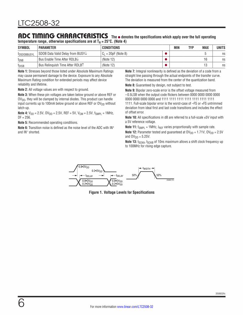
Note 1: Stresses beyond those listed under Absolute Maximum Ratings may cause permanent damage to the device. Exposure to any Absolute Maximum Rating condition for extended periods may affect device reliability and lifetime.Note 2: All voltage values are with respect to ground.Note 3: When these pin voltages are taken below ground or above REF or OVDD, they will be clamped by internal diodes. This product can handle input currents up to 100mA below ground or above REF or OVDD without latch-up.Note 4: VDD = 2.5V, OVDD = 2.5V, REF = 5V, VCM = 2.5V, fSMPL = 1MHz, DF = 256.Note 5: Recommended operating conditions.Note 6: Transition noise is defined as the noise level of the ADC with IN+ and IN– shorted.
Note 7: Integral nonlinearity is defined as the deviation of a code from a straight line passing through the actual endpoints of the transfer curve. The deviation is measured from the center of the quantization band.Note 8: Guaranteed by design, not subject to test. Note 9: Bipolar zero-scale error is the offset voltage measured from –0.5LSB when the output code flickers between 0000 0000 0000 0000 0000 0000 0000 0000 and 1111 1111 1111 1111 1111 1111 1111 1111. Full-scale bipolar error is the worst-case of –FS or +FS untrimmed deviation from ideal first and last code transitions and includes the effect of offset error.Note 10: All specifications in dB are referred to a full-scale ±5V input with a 5V reference voltage.Note 11: fSMPL = 1MHz, IREF varies proportionally with sample rate.Note 12: Parameter tested and guaranteed at OVDD = 1.71V, OVDD = 2.5V and OVDD = 5.25V.Note 13: tSCKA, tSCKB of 10ns maximum allows a shift clock frequency up to 100MHz for rising edge capture.
0.8•OVDD0.2•OVDD
50% 50%
250832 F01
0.2•OVDD0.8•OVDD
0.2•OVDD0.8•OVDD
tDELAY
tWIDTH
tDELAY
Figure 1. Voltage Levels for Specifications

LTC2508-32
7250832fc
For more information www.linear.com/LTC2508-32
TYPICAL PERFORMANCE CHARACTERISTICS
Integral Nonlinearity vs Input Voltage
Integral Nonlinearity vs Input Voltage DC Histogram, DF = 256
DC Histogram, DF = 1024 DC Histogram, DF = 4096 DC Histogram, DF = 16384
128k Point FFT fSMPL = 1Msps, fIN = 200Hz, DF = 256
128k Point FFT fSMPL = 1Msps, fIN = 50Hz, DF = 1024
TA = 25°C, VDD = 2.5V, OVDD = 2.5V, VCM = 2.5V, REF = 5V, fSMPL = 1Msps, DF = 256, Filtered Output, unless otherwise noted.
INPUT VOLTAGE (V)250832 G01
–5 –2.5 0 2.5 5–2.0
–1.5
–1.0
–0.5
0
0.5
1.0
1.5
2.0
INL
ERRO
R (p
pm)
σ = 0.095ppm
OUTPUT CODE (ppm)–0.4 –0.2 0 0.2 0.40
200
400
600
800
1000
COUN
TS
250832 G04
σ = 0.055ppm
OUTPUT CODE (ppm)–0.4 –0.2 0 0.2 0.40
200
400
600
800
1000
COUN
TS
250832 G05
σ = 0.03ppm
OUTPUT CODE (ppm)–0.4 –0.2 0 0.2 0.40
200
400
600
800
1000
COUN
TS
250832 G06
σ = 0.02ppm
OUTPUT CODE (ppm)–0.4 –0.2 0 0.2 0.40
200
400
600
800
1000
COUN
TS
250832 G07
250832 G08
DR = 131dB
FREQUENCY (kHz)0 0.5 1 1.5 2
–200
–180
–160
–140
–120
–100
–80
–60
–40
–20
0
AMPL
ITUD
E (d
BFS)
250832 G09
DR = 136dB
FREQUENCY (Hz)0 122 244 366 488
–200
–180
–160
–140
–120
–100
–80
–60
–40
–20
0
AMPL
ITUD
E (d
BFS)
ARBITRARY DRIVEIN+/IN– SWEPT 0 TO 5V
INPUT VOLTAGE (V)–5 –2.5 0 2.5 5
–3.5
–1.8
0
1.8
3.5
INL
ERRO
R (p
pm)
250832 G03
32k Point FFT fSMPL = 1Msps, fIN = 10Hz, DF = 4096
250832 G09
DR = 141dB
FREQUENCY (Hz)0 30 61 91 122
–200
–180
–160
–140
–120
–100
–80
–60
–40
–20
0
AMPL
ITUD
E (d
BFS)
LTC2508-32
8250832fc
For more information www.linear.com/LTC2508-32
8k Point FFT fSMPL = 1Msps, fIN = 10Hz, DF = 16384
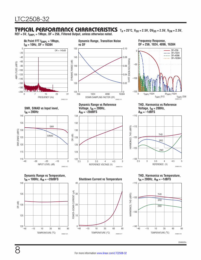
Dynamic Range, Transition Noise vs DF
Frequency Response, DF = 256, 1024, 4096, 16384
SNR, SINAD vs Input level, fIN = 200Hz
Dynamic Range vs Reference Voltage, fIN = 200Hz, AIN = –20dBFS
THD, Harmonics vs Reference Voltage, fIN = 200Hz, AIN = –1dBFS
Dynamic Range vs Temperature, fIN = 100Hz, AIN = –20dBFS
TYPICAL PERFORMANCE CHARACTERISTICS TA = 25°C, VDD = 2.5V, OVDD = 2.5V, VCM = 2.5V, REF = 5V, fSMPL = 1Msps, DF = 256, Filtered Output, unless otherwise noted.
Shutdown Current vs TemperatureTHD, Harmonics vs Temperature, fIN = 200Hz, AIN = –1dBFS
250832 G10
DR = 145dB
FREQUENCY (Hz)0 7 15 23 31
–200
–180
–160
–140
–120
–100
–80
–60
–40
–20
0
AMPL
ITUD
E (d
BFS)
250832 G11DOWN SAMPLING FACTOR (DF)
256 1024 4096 16384125
130
135
140
145
150
0
0.02
0.04
0.06
0.08
0.10
DYNA
MIC
RAN
GE (d
B)TRANSITION NOISE (ppm
)
250832 G14REFERENCE VOLTAGE (V)
2.5 3 3.5 4 4.5 5122
124
126
128
130
132
134
DR (d
B)
250832 G15
THD
3RD
2ND
REFERENCE (V)2.5 3 3.5 4 4.5 5
–130
–125
–120
–115
–110
HARM
ONIC
S, T
HD (d
BFS)
250832 G16TEMPERATURE (oC)
–40 –15 10 35 60 85120
125
130
135
140
DR (d
B)
250832 G18
THD
3RD
2ND
TEMPERATURE (oC)
–40 –15 10 35 60 85–140
–130
–120
–110
HARM
ONIC
S, T
HD (d
BFS)
250832 G12
0 fSMPL/1024fSMPL/512
3fSMPL/1024fSMPL/256
–150
–100
–50
0
DF=16384DF=4096DF=1024DF=256
250832 G13
SNR
SINAD
INPUT LEVEL (dB)–40 –30 –20 –10 0
110
115
120
125
130
135
140
SNR,
SINA
D (d
BFS)
TEMPERATURE (°C)
–40 –15 10 35 60 850
10
20
30
40
POW
ER–D
OWN
CURR
ENT
(µA)
250832 G17

LTC2508-32
9250832fc
For more information www.linear.com/LTC2508-32
TYPICAL PERFORMANCE CHARACTERISTICS
INL vs Temperature Full-Scale Error vs Temperature Offset Error vs Temperature
Supply Current vs TemperatureCommon Mode Rejection vs Input Frequency
Reference Current vs Reference Voltage
TA = 25°C, VDD = 2.5V, OVDD = 2.5V, VCM = 2.5V, REF = 5V, fSMPL = 1Msps, DF = 256, Filtered Output, unless otherwise noted.
MAX INL
MIN INL
TEMPERATURE (°C)
–40 –15 10 35 60 85–4
–3
–2
–1
0
1
2
3
4
INL
ERRO
R (p
pm)
250832 G19 250832 G20
–FS
+FS
TEMPERATURE (oC)
–40 –15 10 35 60 85–10
–5
0
5
10
FULL
–SCA
LE E
RROR
(ppm
)
TEMPERATURE (°C)
–40 –15 10 35 60 85–5
–4
–3
–2
–1
0
1
2
3
4
5
ZERO
–SCA
LE E
RROR
(ppm
)
250832 G21
I VDD
I REF
TEMPERATURE (°C)
–40 –15 10 35 60 850
1
2
3
4
5
6
7
8
9
10
POW
ER S
UPPL
Y CU
RREN
T (m
A)
I OVDD
250832 G22FREQUENCY (MHz)
0.0001 0.001 0.01 0.1 1 275
100
125
150
175
200
CMRR
(dB)
250832 G23REFERENCE VOLTAGE (V)
2.5 3 3.5 4 4.5 50
0.1
0.2
0.3
0.4
0.5
0.6
0.7
0.8
0.9
1.0
REFE
RENC
E CU
RREN
T (A
)
250832 G24
LTC2508-32
10250832fc
For more information www.linear.com/LTC2508-32
TYPICAL PERFORMANCE CHARACTERISTICS
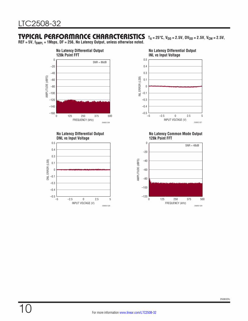
No Latency Differential Output INL vs Input Voltage
No Latency Differential Output DNL vs Input Voltage
No Latency Common Mode Output 128k Point FFT
TA = 25°C, VDD = 2.5V, OVDD = 2.5V, VCM = 2.5V, REF = 5V, fSMPL = 1Msps, DF = 256, No Latency Output, unless otherwise noted.
INPUT VOLTAGE (V)–5 –2.5 0 2.5 5
–0.5
–0.4
–0.3
–0.1
0
0.1
0.3
0.4
0.5
INL
ERRO
R (L
SB)
250832 G27
INPUT VOLTAGE (V)–5 –2.5 0 2.5 5
–0.5
–0.4
–0.3
–0.1
0
0.1
0.3
0.4
0.5
DNL
ERRO
R (L
SB)
250832 G28
SNR = 48dB
FREQUENCY (kHz)0 125 250 375 500
–120
–100
–80
–60
–40
–20
0
AMPL
ITUD
E (d
BFS)
250832 G29
No Latency Differential Output 128k Point FFT
SNR = 86dB
FREQUENCY (kHz)0 125 250 375 500
–160
–140
–120
–100
–80
–60
–40
–20
0
AMPL
ITUD
E (d
BFS)
250832 G26
LTC2508-32
11250832fc
For more information www.linear.com/LTC2508-32
PIN FUNCTIONSRDLA (Pin 1): Read Low Input A (Filtered Output). When RDLA is low, the serial data output A (SDOA) pin is enabled. When RDLA is high, SDOA pin is in a high-impedance state. Logic levels are determined by OVDD.
RDLB (Pin 2): Read Low Input B (No Latency Output). When RDLB is low, the serial data output B (SDOB) pin is enabled. When RDLB is high, SDOB pin is in a high-impedance state. Logic levels are determined by OVDD.
VDD (Pin 3): 2.5V Power Supply. The range of VDD is 2.375V to 2.625V. Bypass VDD to GND with a 10µF ce-ramic capacitor.
GND (Pins 4, 7, 16, 23, 24): Ground.
IN+ (Pin 5): Positive Analog Input.
IN– (Pin 6): Negative Analog Input.
REF (Pins 8, 9, 10): Reference Input. The range of REF is 2.5V to 5.1V. This pin is referred to the GND pin and should be decoupled closely to the pin with a 47µF ceramic capacitor (X7R, 1210 size, 10V rating).
SEL0, SEL1 (Pins 11, 12): Down-Sampling Factor Select Input 0, Down-Sampling Factor Select Input 1. Selects the down-sampling factor for the digital filter. Down-sampling factors of 256, 1024, 4096 and 16384 are selected for [SEL0 SEL1] combinations of 00, 01, 10 and 11 respec-tively. Logic levels are determined by OVDD.
MCLK (Pin 13): Master Clock Input. A rising edge on this input powers up the part and initiates a new conversion. Logic levels are determined by OVDD.
SYNC (Pin 14): Synchronization Input. A pulse on this input is used to synchronize the phase of the digital filter. Logic levels are determined by OVDD.
DRL (Pin 15): Data Ready Low Output. A falling edge on this pin indicates that a new filtered output code is available in the output register of SDOA. Logic levels are determined by OVDD.
SDOA (Pin 17): Serial Data Output A (Filtered Output). The filtered output code appears on this pin (MSB first) on each rising edge of SCKA. The output data is in 2’s complement format. Logic levels are determined by OVDD.
SCKA (Pin 18): Serial Data Clock Input A (Filtered Output). When SDOA is enabled, the filtered output code is shifted out (MSB first) on the rising edges of this clock. Logic levels are determined by OVDD.
SCKB (Pin 19): Serial Data Clock Input B (No Latency Output). When SDOB is enabled, the no latency output code is shifted out (MSB first) on the rising edges of this clock. Logic levels are determined by OVDD.
SDOB (Pin 20): Serial Data Output B (No Latency Output). The 22-bit no latency composite output code appears on this pin (MSB first) on each rising edge of SCKB. The output data is in 2’s complement format. Logic levels are determined by OVDD.
BUSY (Pin 21): BUSY Indicator. Goes high at the start of a new conversion and returns low when the conversion has finished. Logic levels are determined by OVDD.
OVDD (Pin 22): I/O Interface Digital Power. The range of OVDD is 1.71V to 5.25V. This supply is nominally set to the same supply as the host interface (1.8V, 2.5V, 3.3V, or 5V). Bypass OVDD to GND (Pin 23) close to the pin with a 0.1µF capacitor.
GND (Exposed Pad Pin 25): Ground. Exposed pad must be soldered directly to the ground plane.

LTC2508-32
12250832fc
For more information www.linear.com/LTC2508-32
FUNCTIONAL BLOCK DIAGRAM
TIMING DIAGRAM
IN+
REF = 5V VDD = 2.5V OVDD = 1.8V TO 5V
IN–
32-BITSAR ADC
SCKA
SDOA
RDLA
LTC2508-32
SPIPORT
+
–
MCLK
BUSY
DRL
SYNC
SEL0
SEL1
250832 FBD
GND
CONTROL LOGIC
SCKB
SDOB
RDLB
DIGITALFILTER
14
32
DA31 DA29 DA27 DA25 DA23 DA21 DA19 DA17 DA15 DA13 DA11 DA9 DA7 DA5 DA3 DA1 WA7 WA5 WA3 WA1
DA30 DA28 DA26 DA24 DA22 DA20 DA18 DA16 DA14 DA12 DA10 DA8 DA6 DA4 DA2 DA0 WA6 WA4 WA2 WA0
DB13
MCLK
DRL
RDLA = RDLB = 0
CONVERT
SCKA
SDOA
SCKB
SDOB
BUSY
DB11 DB9 DB7 DB5 DB3 DB1 CB7 CB5 CB3 250832 TD
DB12 DB10 DB8 DB6 DB4 DB2 DB0 CB6 CB4 CB2
CB1
CB0
CONVERT
POWER DOWN AND ACQUIRE
Conversion Timing Using the Serial Interface

LTC2508-32
13250832fc
For more information www.linear.com/LTC2508-32
Figure 2. LTC2508-32 Transfer Function
APPLICATIONS INFORMATIONOVERVIEW
The LTC2508-32 is a low noise, low power, high-perfor-mance 32-bit ADC with an integrated configurable digital filter. Operating from a single 2.5V supply, the LTC2508-32 features a fully differential input range up to ±VREF, with VREF ranging from 2.5V to 5.1V. The LTC2508-32 supports a wide common mode range from 0V to VREF simplifying analog signal conditioning requirements.
The LTC2508-32 simultaneously provides two output codes: (1) a 32-bit digitally filtered high precision low noise code, and (2) a 22-bit no latency composite code. The configurable digital filter reduces measurement noise by lowpass filtering and down-sampling the stream of data from the SAR ADC core, giving the 32-bit filtered output code. The 22-bit composite code consists of a 14-bit code representing the differential voltage and an 8-bit code representing the common mode voltage. The 22-bit composite code is available each conversion cycle, with no cycle of latency.
The digital filter can be easily configured for 4 different down-sampling factors by pin strapping. The configura-tions provide a dynamic range of 131dB at 3.9ksps and 145dB at 61sps. The digital lowpass filter relaxes the re-quirements for analog anti-aliasing. Multiple LTC2508-32 devices can be easily synchronized using the SYNC pin.
CONVERTER OPERATION
The LTC2508-32 operates in two phases. During the ac-quisition phase, a 32-bit charge redistribution capacitor D/A converter (CDAC) is connected to the IN+ and IN– pins to sample the analog input voltages. A rising edge on the MCLK pin initiates a conversion. During the conversion phase, the 32-bit CDAC is sequenced through a succes-sive approximation algorithm, effectively comparing the sampled inputs with binary-weighted fractions of the refer-ence voltage (e.g. VREF/2, VREF/4 … VREF/4294967296). At the end of conversion, the CDAC output approximates the sampled analog input. The ADC control logic then passes the 32-bit digital output code to the digital filter for further processing. A 14-bit code representing the differential voltage and an 8-bit code representing the common mode
voltage are combined to form a 22-bit composite code. The 22-bit composite code is available each conversion cycle, without any cycle of latency.
TRANSFER FUNCTION
The LTC2508-32 digitizes the full-scale differential voltage of 2× VREF into 232 levels, resulting in an LSB size of 2.3nV with a 5V reference. The ideal transfer function is shown in Figure 2. The output data is in 2’s complement format.
ANALOG INPUT
The LTC2508-32 samples the voltage difference (IN+ – IN–) between its analog input pins over a wide common mode input range while attenuating unwanted signals common to both input pins by the common-mode rejec-tion ratio (CMRR) of the ADC. Wide common mode input range coupled with high CMRR allows the IN+/IN– analog inputs to swing with an arbitrary relationship to each other, provided each pin remains between GND and VREF. This unique feature of the LTC2508-32 enables it to accept a wide variety of signal swings, including traditional classes of analog input signals such as pseudo-differential unipo-lar, pseudo-differential true bipolar, and fully differential, thereby simplifying signal chain design.
In the acquisition phase, each input sees approximately 45pF (CIN) from the sampling circuit in series with 40Ω (RON) from the on-resistance of the sampling switch.
INPUT VOLTAGE (V)
0V
OUTP
UT C
ODE
(TW
O’S
COM
PLEM
ENT)
–1 LSB
250832 F02
011...111
011...110
000...001
000...000
100...000
100...001
111...110
1LSB
BIPOLARZERO
111...111
FSR/2 – 1LSB–FSR/2
FSR = +FS – –FS1LSB = FSR/4294967296

LTC2508-32
14250832fc
For more information www.linear.com/LTC2508-32
APPLICATIONS INFORMATION
The inputs draw a current spike while charging the CIN capacitors during acquisition. During conversion, the analog inputs draw only a small leakage current.
INPUT DRIVE CIRCUITS
A low impedance source can directly drive the high imped-ance inputs of the LTC2508-32 without gain error. A high impedance source should be buffered to minimize settling time during acquisition and to optimize ADC linearity. For best performance, a buffer amplifier should be used to drive the analog inputs of the LTC2508-32. The amplifier provides low output impedance, which produces fast settling of the analog signal during the acquisition phase. It also provides isolation between the signal source and the ADC inputs.
Noise and Distortion
The noise and distortion of an input buffer amplifier and other supporting circuitry must be considered since they add to the ADC noise and distortion. Noisy input signals should be filtered prior to the buffer amplifier with a low bandwidth filter to minimize noise. The simple one-pole RC lowpass filter (LPF1) shown in Figure 4 is sufficient for many applications.
A coupling filter network (LPF2) should be used between the buffer and ADC input to minimize disturbances reflected into the buffer from sampling transients. Long RC time constants at the analog inputs will slow down the settling
REF
250832 F03
REFBIASVOLTAGE
IN+
IN–
RON40Ω
CIN45pF
RON40Ω
CIN45pF
Figure 3. The Equivalent Circuit for the Differential Analog Input of the LTC2508-32
Figure 4. Filtering Input Signal
of the analog inputs. Therefore, LPF2 typically requires wider bandwidth than LPF1. This filter also helps minimize the noise contribution from the buffer. A buffer amplifier with a low noise density must be selected to minimize degradation of SNR.
10Ω
3300pF
6600pF10Ω
500Ω
LPF2
LPF1
BW = 1.2MHzBW = 48kHz
SINGLE-ENDED-TO-DIFFERENTIAL
DRIVER
SINGLE-ENDED-INPUT SIGNAL
LTC2508-32
IN+
IN–
250832 F04
6800pF
6800pF
High quality capacitors and resistors should be used in the RC filters since these components can add distortion. NPO and silver mica type dielectric capacitors have excellent linearity. Carbon surface mount resistors can generate distortion from self-heating and from damage that may occur during soldering. Metal film surface mount resistors are much less susceptible to both problems.
Input Currents
An important consideration when coupling an amplifier to the LTC2508-32 is in dealing with current spikes drawn by the ADC inputs at the start of each acquisition phase. The ADC inputs may be modeled as a switched capacitor load of the drive circuit. A drive circuit may rely partially on attenuating switched-capacitor current spikes with small filter capacitors CFILT placed directly at the ADC inputs, and partially on the driver amplifier having suffi-cient bandwidth to recover from the residual disturbance. Amplifiers optimized for DC performance may not have sufficient bandwidth to fully recover at the ADC’s maximum conversion rate, which can produce nonlinearity and other errors. Coupling filter circuits may be classified in three broad categories:

LTC2508-32
15250832fc
For more information www.linear.com/LTC2508-32
APPLICATIONS INFORMATION
Figure 5. Equivalent Circuit for the Differential Analog Input of the LTC2508-32 at 1Msps
Figure 6. Common Mode and Differential Input Leakage Current Over Temperature
Fully Settled – This case is characterized by filter time constants and an overall settling time that is consider-ably shorter than the sample period. When acquisition begins, the coupling filter is disturbed. For a typical first order RC filter, the disturbance will look like an initial step with an exponential decay. The amplifier will have its own response to the disturbance, which may include ringing. If the input settles completely (to within the accuracy of the LTC2508-32), the disturbance will not contribute any error.
Partially Settled – In this case, the beginning of acquisi-tion causes a disturbance of the coupling filter, which then begins to settle out towards the nominal input voltage. However, acquisition ends (and the conversion begins) before the input settles to its final value. This generally produces a gain error, but as long as the settling is linear, no distortion is produced. The coupling filter’s response is affected by the amplifier’s output impedance and other parameters. A linear settling response to fast switched- capacitor current spikes can NOT always be assumed for precision, low bandwidth amplifiers. The coupling filter serves to attenuate the current spikes’ high-frequency energy before it reaches the amplifier.
Fully Averaged – If the coupling filter capacitors (CFILT) at the ADC inputs are much larger than the ADC’s sample capacitors (45pF), then the sampling glitch is greatly at-tenuated. The driving amplifier effectively only sees the average sampling current, which is quite small. At 1Msps, the equivalent input resistance is approximately 22kΩ (as shown in Figure 5), a benign resistive load for most precision amplifiers. However, resistive voltage division will occur between the coupling filter’s DC resistance and the ADC’s equivalent (switched-capacitor) input resistance, thus producing a gain error.
The input leakage currents of the LTC2508-32 should also be considered when designing the input drive circuit, because source impedances will convert input leakage currents to an added input voltage error. The input leakage currents, both common mode and differential, are typically extremely small over the entire operating temperature range. Figure 6 shows the input leakage currents over temperature for a typical part.
CFILT>>45pF
LTC2508-32
BIASVOLTAGE
IN+
22kΩ(REQ)
22kΩ(REQ)
IN–
CFILT>>45pF
REQ = fSMPL • 45pF1
Let RS1 and RS2 be the source impedances of the dif-ferential input drive circuit shown in Figure 7, and let IL1 and IL2 be the leakage currents flowing out of the ADC’s analog inputs. The differential voltage error, VE, due to the leakage currents can be expressed as:
VE =
RS1+RS22
• IL1–IL2( )+ RS1–RS2( ) • IL1+IL22
The common mode input leakage current, (IL1 + IL2)/2, is typically extremely small (Figure 6) over the entire operat-ing temperature range and common mode input voltage range. Thus, any reasonable mismatch (below 5%) of the source impedances RS1 and RS2 will cause only a negligible error. The differential leakage current is also typically very small, and its nonlinear component is even smaller. Only the nonlinear component will impact the ADC’s linearity.
COMMON
VIN = VREF
DIFFERENTIAL
TEMPERATURE (°C) 250832 F06
–40 –15 10 35 60 85–5
–2
1
4
7
10
INPU
T LE
AKAG
E (n
A)

LTC2508-32
16250832fc
For more information www.linear.com/LTC2508-32
APPLICATIONS INFORMATION
For optimal performance, it is recommended that the source impedances, RS1 and RS2, be between 5Ω and 50Ω and with 1% tolerance. For source impedances in this range, the voltage and temperature coefficients of RS1 and RS2 are usually not critical. The guaranteed AC and DC specifications are tested with 5Ω source imped-ances, and the specifications will gradually degrade with increased source impedances due to incomplete settling.
DC Accuracy
The LTC2508-32 has excellent INL specifications. This makes the LTC2508-32 ideal for applications which re-quire high DC accuracy, including parameters such as offset and offset drift. To maintain high accuracy over the entire DC signal chain, amplifiers have to be selected very carefully. A large-signal open-loop gain of at least 126dB may be required to ensure 1ppm linearity for amplifiers configured for a gain of negative 1. However, less gain is sufficient if the amplifier’s gain characteristic is known to
RS1
RS2
IL1
IL2
250832 F07
IN+
VE
IN–
+
–LTC2508-32
Figure 7. Source Impedances of a Driver and Input Leakage Currents of the LTC2508-32
Figure 8. Buffering Two Analog Input Signals
2.5V
IN+
IN–
REF GND
LTC2508-32
VDD OVDD
10µF 0.1µF
1.8V TO 5.1V
2.5V TO 5.1V
250832 F08
47µF(X7R, 1210 SIZE)
VIN+
–
+
+
–
4.7µF
0.047µF
0.047µF
4.99k
4.99k
10ΩLTC2057
LTC205710Ω
4.7µFVIN–
be (mostly) linear. An amplifier’s offset versus signal level must be considered for amplifiers configured as unity gain buffers. For example, 1ppm linearity may require that the offset is known to vary less than 5μV for a 5V swing. However, greater offset variations may be acceptable if the relationship is known to be (mostly) linear. Unity-gain buffer amplifiers typically require substantial headroom to the power supply rails for best performance. Inverting ampli-fier circuits configured to minimize swing at the amplifier input terminals may perform better with less headroom than unity-gain buffer amplifiers. The linearity and thermal properties of an inverting amplifier’s feedback network should be considered carefully to ensure DC accuracy.
Buffering Input Signals
The wide common mode input range and high CMRR of the LTC2508-32 allow analog inputs IN+ and IN– pins to swing with an arbitrary relationship to each other, provided that each pin remains between VREF and GND. This unique feature of the LTC2508-32 enables it to accept a wide variety of signal swings, simplifying signal chain design.
Buffering DC Accurate Input Signals
Figure 8 shows a typical application where two analog input voltages are buffered using the LTC2057. The LTC2057 is a high precision zero drift amplifier which complements the low offset and offset drift of the LTC2508-32. The LTC2057 is shown in a non-inverting amplifier configura-
LTC2508-32
17250832fc
For more information www.linear.com/LTC2508-32
APPLICATIONS INFORMATION
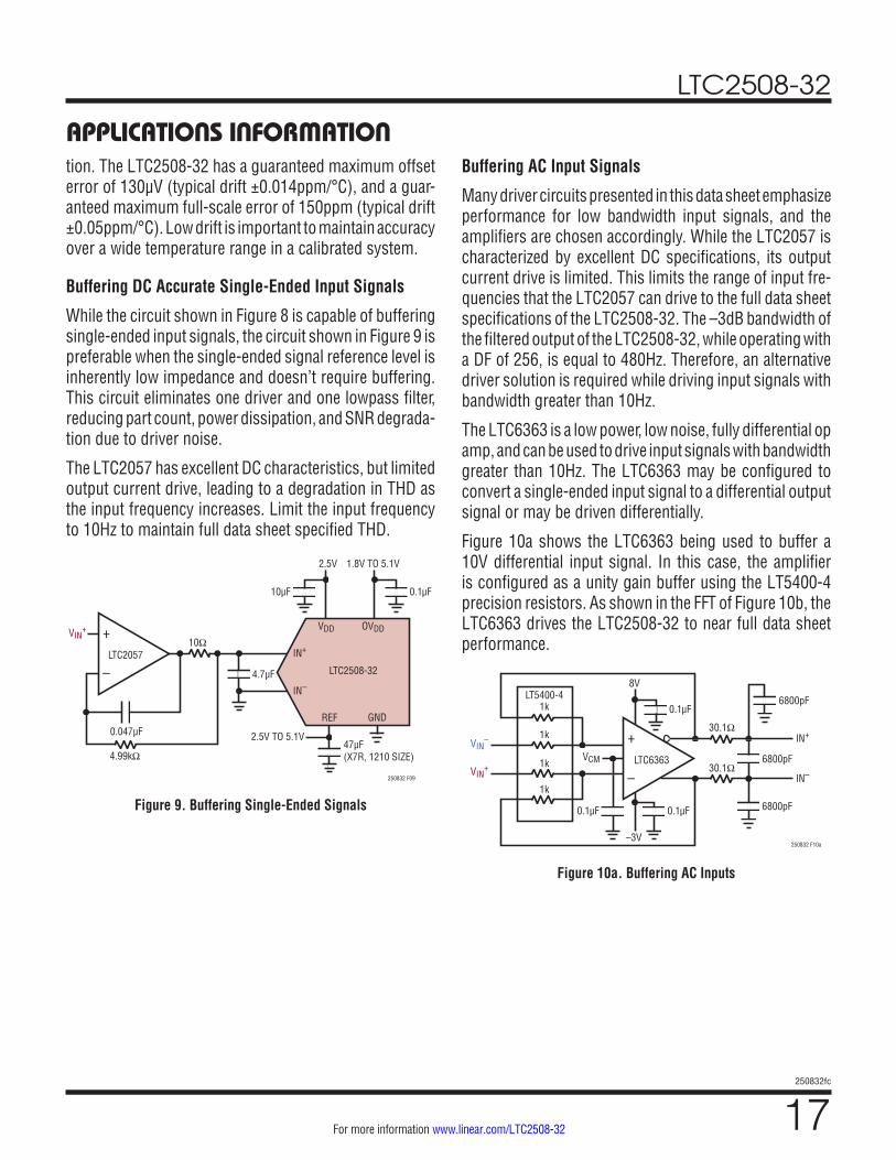
Figure 10a. Buffering AC Inputs
tion. The LTC2508-32 has a guaranteed maximum offset error of 130µV (typical drift ±0.014ppm/°C), and a guar-anteed maximum full-scale error of 150ppm (typical drift ±0.05ppm/°C). Low drift is important to maintain accuracy over a wide temperature range in a calibrated system.
Buffering DC Accurate Single-Ended Input Signals
While the circuit shown in Figure 8 is capable of buffering single-ended input signals, the circuit shown in Figure 9 is preferable when the single-ended signal reference level is inherently low impedance and doesn’t require buffering. This circuit eliminates one driver and one lowpass filter, reducing part count, power dissipation, and SNR degrada-tion due to driver noise.
The LTC2057 has excellent DC characteristics, but limited output current drive, leading to a degradation in THD as the input frequency increases. Limit the input frequency to 10Hz to maintain full data sheet specified THD.
Figure 9. Buffering Single-Ended Signals
2.5V
IN+
IN–
REF GND
LTC2508-32
VDD OVDD
10µF
4.7µF
0.047µF
4.99kΩ
10ΩVIN
+
0.1µF
250832 F09
1.8V TO 5.1V
2.5V TO 5.1V47µF(X7R, 1210 SIZE)
–
+LTC2057
Buffering AC Input Signals
Many driver circuits presented in this data sheet emphasize performance for low bandwidth input signals, and the amplifiers are chosen accordingly. While the LTC2057 is characterized by excellent DC specifications, its output current drive is limited. This limits the range of input fre-quencies that the LTC2057 can drive to the full data sheet specifications of the LTC2508-32. The –3dB bandwidth of the filtered output of the LTC2508-32, while operating with a DF of 256, is equal to 480Hz. Therefore, an alternative driver solution is required while driving input signals with bandwidth greater than 10Hz.
The LTC6363 is a low power, low noise, fully differential op amp, and can be used to drive input signals with bandwidth greater than 10Hz. The LTC6363 may be configured to convert a single-ended input signal to a differential output signal or may be driven differentially.
Figure 10a shows the LTC6363 being used to buffer a 10V differential input signal. In this case, the amplifier is configured as a unity gain buffer using the LT5400-4 precision resistors. As shown in the FFT of Figure 10b, the LTC6363 drives the LTC2508-32 to near full data sheet performance.
LT5400-41k 0.1µF
0.1µF
–3V
0.1µF
8V
VCM
6800pF
6800pF
6800pF
250832 F10a
IN+VIN
–
VIN+
IN–
30.1Ω
30.1Ω
1k
1k
1k–
+LTC6363

LTC2508-32
18250832fc
For more information www.linear.com/LTC2508-32
APPLICATIONS INFORMATION
Figure 10b. 128k Point FFT with fIN = 200Hz for Circuit Shown in Figure 10a
Figure 11. MCLK Waveform Showing Burst Sampling
ADC REFERENCE
An external reference defines the input range of the LTC2508-32. A low noise, low temperature drift reference is critical to achieving the full data sheet performance of the ADC. Linear Technology offers a portfolio of high performance references designed to meet the needs of many applications. With its small size, low power and high accuracy, the LTC6655-5 is particularly well suited for use with the LTC2508-32. The LTC6655-5 offers 0.025% (max) initial accuracy and 2ppm/°C (max) temperature coefficient for high precision applications.
When choosing a bypass capacitor for the LTC6655-5, the capacitor’s voltage rating, temperature rating, and pack-age size should be carefully considered. Physically larger capacitors with higher voltage and temperature ratings tend to provide a larger effective capacitance, better filtering the noise of the LTC6655-5, and consequently facilitating a higher SNR. Therefore, we recommend bypassing the LTC6655-5 with a 47μF ceramic capacitor (X7R, 1210 size, 10V rating) close to the REF pin.
The REF pin of the LTC2508-32 draws charge (QCONV) from the 47μF bypass capacitor during each conversion cycle.
MCLK
250832 F11
IDLEPERIOD
IDLEPERIOD
The reference replenishes this charge with an average current, IREF = QCONV/tCYC. The current drawn from the REF pin, IREF, depends on the sampling rate and output code. If the LTC2508-32 continuously samples a signal at a constant rate, the LTC6655-5 will keep the deviation of the reference voltage over the entire code span to less than 0.5ppm.
When idling, the REF pin on the LTC2508-32 draws only a small leakage current (< 1μA). In applications where a burst of samples is taken after idling for long periods as shown in Figure 11, IREF quickly goes from approximately 0μA to a maximum of 1mA at 1Msps. This step in average current drawn causes a transient response in the refer-ence that must be considered, since any deviation in the reference output voltage will affect the accuracy of the output code. In applications where the transient response of the reference is important, the fast settling LTC6655-5 reference is also recommended.
Reference Noise
The dynamic range of the ADC will increase approximately 6dB for every 4× increase in the down-sampling factor (DF). The SNR should also improve as a function of DF in the same manner. For large input signals near full-scale, however, any reference noise will limit the improvement of the SNR as DF increases, because any noise on the REF pin will modulate around the fundamental frequency of the input signal. Therefore, it is critical to use a low-noise refer-ence, especially if the input signal amplitude approaches full-scale. For small input signals, the dynamic range will improve as described earlier in this section.
DYNAMIC PERFORMANCE
Fast Fourier Transform (FFT) techniques are used to test the ADC’s frequency response, distortion and noise at the rated throughput. By applying a low distortion sine wave and analyzing the digital output using an FFT algorithm,
250832 F10b
DR = 130dB
FREQUENCY (kHz)0 0.5 1 1.5 2
–200
–180
–160
–140
–120
–100
–80
–60
–40
–20
0
AMPL
ITUD
E (d
BFS)

LTC2508-32
19250832fc
For more information www.linear.com/LTC2508-32
APPLICATIONS INFORMATION
Figure 12. 128k Point FFT Plot of LTC2508-32 with DF = 256, fIN = 200Hz and fSMPL = 1MHz
the ADC’s spectral content can be examined for frequen-cies outside the fundamental. The LTC2508-32 provides guaranteed tested limits for both AC distortion and noise measurements.
Dynamic Range
The dynamic range is the ratio of the RMS value of a full scale input to the total RMS noise measured with the inputs shorted to VREF/2. The dynamic range of the LTC2508-32 with DF = 256 is 131dB which improves with increase in the down-sampling factor.
Signal-to-Noise and Distortion Ratio (SINAD)
The signal-to-noise and distortion ratio (SINAD) is the ratio between the RMS amplitude of the fundamental input frequency and the RMS amplitude of all other frequency components at the ADC output. The output is band-limited to frequencies from above DC and below half the sampling frequency. Figure 12 shows that the LTC2508-32 achieves a typical SINAD of 120dB at a 1MHz sampling rate with a 200Hz input, and DF = 256.
Total Harmonic Distortion (THD)
Total Harmonic Distortion (THD) is the ratio of the RMS sum of all harmonics of the input signal to the fundamental itself. The out-of-band harmonics alias into the frequency band between DC and half the sampling frequency (fSMPL/2). THD is expressed as:
THD=20LOG V22+V32+V42+!+VN2
V1 where V1 is the RMS amplitude of the fundamental frequency and V2 through VN are the amplitudes of the second through Nth harmonics.
POWER CONSIDERATIONS
The LTC2508-32 has two power supply pins: the 2.5V power supply (VDD), and the digital input/output interface power supply (OVDD). The flexible OVDD supply allows the LTC2508-32 to communicate with any digital logic operating between 1.8V and 5V, including 2.5V and 3.3V systems.
Power Supply Sequencing
The LTC2508-32 does not have any specific power sup-ply sequencing requirements. Care should be taken to adhere to the maximum voltage relationships described in the Absolute Maximum Ratings section. The LTC2508-32 has a power-on-reset (POR) circuit that will reset the LTC2508-32 at initial power-up or whenever the power supply voltage drops below 1V. Once the supply voltage re-enters the nominal supply voltage range, the POR will reinitialize the ADC. No conversions should be initiated until 200μs after a POR event to ensure the reinitialization period has ended. Any conversions initiated before this time will produce invalid results.
TIMING AND CONTROL
MCLK Timing
A rising edge on MCLK will power up the LTC2508-32 and start a conversion. Once a conversion has been started, further transitions on MCLK are ignored until the conversion is complete. For best results, the falling edge
Signal-to-Noise Ratio (SNR)
The signal-to-noise ratio (SNR) is the ratio between the RMS amplitude of the fundamental input frequency and the RMS amplitude of all other frequency components except the first five harmonics and DC. Figure 12 shows that the LTC2508-32 achieves an SNR of 128dB when sampling a 200Hz input at a 1MHz sampling rate with DF = 256.
250832 F12
SNR = 128dB
FREQUENCY (kHz)0 0.5 1 1.5 2
–200
–180
–160
–140
–120
–100
–80
–60
–40
–20
0
AMPL
ITUD
E (d
BFS)
LTC2508-32
20250832fc
For more information www.linear.com/LTC2508-32
APPLICATIONS INFORMATIONof MCLK should occur within 40ns from the start of the conversion, or after the conversion has been completed. For optimum performance, MCLK should be driven by a clean low jitter signal. Converter status is indicated by the BUSY output which remains high while the conversion is in progress. Once the conversion has completed, the LTC2508-32 powers down and begins acquiring the input signal for the next conversion.
Internal Conversion Clock
The LTC2508-32 has internal timing circuity that is trimmed to achieve a maximum conversion time of 652ns. With a maximum sample rate of 1Msps, a minimum acquisition time of 335ns is guaranteed without any external adjust-ments.
Auto Power Down
The LTC2508-32 automatically powers down after a conversion has been completed and powers up once a new conversion is initiated on the rising edge of MCLK. During power-down, data from the last conversion can be clocked out. To minimize power dissipation during power-down, disable SDOA, SDOB and turn off SCKA, SCKB. The auto power-down feature will reduce the power dissipa-tion of the LTC2508-32 as the sampling rate is reduced. Since power is consumed only during a conversion, the LTC2508-32 remains powered down for a larger fraction of the conversion cycle (tCYC) at lower sample rates, thereby reducing the average power dissipation which scales with the sampling rate as shown in Figure 13.
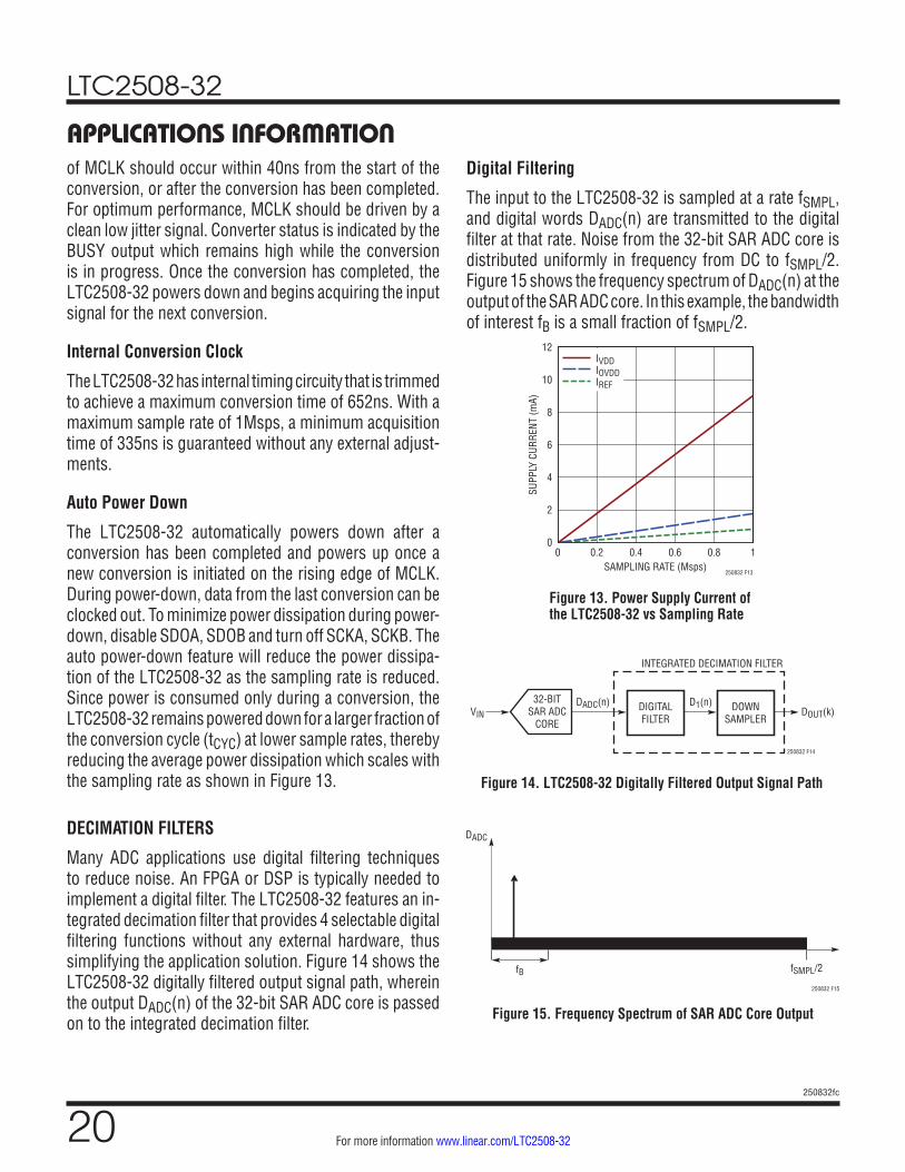
DECIMATION FILTERS
Many ADC applications use digital filtering techniques to reduce noise. An FPGA or DSP is typically needed to implement a digital filter. The LTC2508-32 features an in-tegrated decimation filter that provides 4 selectable digital filtering functions without any external hardware, thus simplifying the application solution. Figure 14 shows the LTC2508-32 digitally filtered output signal path, wherein the output DADC(n) of the 32-bit SAR ADC core is passed on to the integrated decimation filter.
DIGITALFILTER
32-BITSAR ADC
CORE
DOWNSAMPLER
INTEGRATED DECIMATION FILTER
250832 F14
VIN DOUT(k)DADC(n) D1(n)
Figure 14. LTC2508-32 Digitally Filtered Output Signal Path
Figure 15. Frequency Spectrum of SAR ADC Core Output
Figure 13. Power Supply Current of the LTC2508-32 vs Sampling Rate
Digital Filtering
The input to the LTC2508-32 is sampled at a rate fSMPL, and digital words DADC(n) are transmitted to the digital filter at that rate. Noise from the 32-bit SAR ADC core is distributed uniformly in frequency from DC to fSMPL/2. Figure 15 shows the frequency spectrum of DADC(n) at the output of the SAR ADC core. In this example, the bandwidth of interest fB is a small fraction of fSMPL/2.
DADC
250832 F15
fB fSMPL/2
IVDDIOVDDIREF
SAMPLING RATE (Msps)250832 F13
0 0.2 0.4 0.6 0.8 10
2
4
6
8
10
12
SUPP
LY C
URRE
NT (m
A)

LTC2508-32
21250832fc
For more information www.linear.com/LTC2508-32
APPLICATIONS INFORMATION
Figure 16. Frequency Spectrum of Digital Filter Core Output
Figure 17. Time Domain View of Aliasing
D1
DIGITAL FILTER CUTOFF FREQUENCY
250832 F16
fB fSMPL/2
The digital filter integrated in the LTC2508-32 suppresses out-of-band noise power, thereby lowering overall noise and increasing the dynamic range (DR). The lower the filter bandwidth, the lower the noise, and the higher the DR. Figure 16 shows the corresponding frequency spectrum of D1(n) at the output of the digital filter, where noise beyond the cutoff frequency is suppressed by the digital filter.
Down-Sampling
The output data rate of the digital filter is reduced by a down-sampler without causing spectral interference in the bandwidth of interest.
The down-sampler reduces the data rate by passing ev-ery DFth sample to the output, while discarding all other samples. The sampling frequency fO at the output of the down sampler is the ratio of fSMPL and DF, i.e., fO = fSMPL/DF.
The LTC2508-32 enables the user to select DF according to a desired bandwidth of interest. The 4 available con-figurations can be selected by pin strapping pins SEL0 and SEL1. Table 1 summarizes the different decimation filter configurations and properties. When operating at 1.024Msps, the acquisition time (tACQ) of the LTC2508-32 is reduced to 308.5ns and the output data rate correspond-ingly increases. Note that the dynamic range is unchanged as it is only affected by DF and not by sampling rate.
Table 1. Properties of Filters in LTC2508-32
SEL1:SEL0DOWN SAMPLING
FACTOR (DF)
–3dB BANDWIDTH OUTPUT DATA RATE (ODR)
DYNAMIC RANGEfSMPL = 1Msps fSMPL = 1.024Msps fSMPL = 1Msps fSMPL = 1.024Msps00 256 480Hz 491.5Hz 3906sps 4000sps 131dB01 1024 120Hz 122.8Hz 977sps 1000sps 136dB10 4096 30Hz 30.7Hz 244sps 250sps 141dB11 16384 7.5Hz 7.7Hz 61sps 62.5sps 145dB
Aliasing
The maximum bandwidth that a signal being sampled can have and be accurately represented by its samples is the Nyquist bandwidth. The Nyquist bandwidth ranges from DC to half the sampling frequency (a.k.a. the Nyquist frequency). An input signal whose bandwidth exceeds the Nyquist frequency, when sampled, will experience distortion due to an effect called “Aliasing”.
When aliasing, frequency components greater than the Nyquist frequency undergo a frequency shift and appear within the Nyquist bandwidth. Figure 17 illustrates aliasing in the time domain. The solid line shows a sinusoidal input signal of a frequency greater than the Nyquist frequency (fO/2). The circles show the signal sampled at fO. Note that the sampled signal is identical to that of sampling another sinusoidal input signal of a lower frequency shown with the dashed line. To avoid aliasing, it is necessary to band-limit an input signal to the Nyquist bandwidth before sampling it. A filter that suppresses spectral components outside the Nyquist bandwidth is called an “Anti-Aliasing Filter”(AAF).
Anti-Aliasing Filters
Figure 18 shows a typical signal chain including a lowpass AAF and an ADC sampling at a rate of fO. The AAF rejects input signal components exceeding fO/2, thus avoiding aliasing. If the bandwidth of interest is close to fO/2, then
INPUT SIGNAL
250832 F17
SAMPLED SIGNAL(ALIASED)

LTC2508-32
22250832fc
For more information www.linear.com/LTC2508-32
APPLICATIONS INFORMATIONthe AAF must have a very steep roll-off. The complexity of the analog AAF increases with the steepness of the roll-off, and it may be prohibitive if a very steep filter is required.
Alternatively, a simple low-order analog filter in combination with a digital filter can be used to create a mixed-mode equivalent AAF with a very steep roll-off. A mixed-mode filter implementation is shown in Figure 19 where an analog filter with a gradual roll-off is followed by the LTC2508-32 sampling at a rate of fSMPL = DF • fO. The LTC2508-32 has an integrated digital filter at the output of the ADC core. The equivalent AAF, HEQ(f), is the product
of the frequency responses of the analog filter H1(f) and digital filter H2(f), as shown in Figure 20. The digital filter provides a steep roll-off, allowing the analog filter to have a relatively gradual roll-off.
The digital filter in the LTC2508-32 operates at the ADC sampling rate fSMPL and suppresses signals at frequencies exceeding fO/2. The frequency response of the digital filter H2(f) repeats at multiples of fSMPL, resulting in unwanted passbands at each multiple of fSMPL. The analog filter should be designed to provide adequate suppression of the unwanted passbands, such that HEQ(f) has only one passband corresponding to the frequency range of interest. Larger DF settings correspond to less bandwidth of the digital filter, allowing for the analog filter to have a more gradual roll-off. A simple first- or second-order analog filter will provide adequate suppression for most systems.
ANALOG FILTER LTC2508
DIGITAL FILTER
DF
DOWN-SAMPLER
IMAGE
VIN
fSMPL
fSMPL = DF × fO
fSMPL
fSMPL – f0/2
H1H2
D1 (n) DOUT (k)AT f0 (sps)
f0/2 f0/2
fSMPL – f0/2
250832 F19
ADCCORE
ANALOG FILTER DIGITAL FILTER
VIN
fSMPL fSMPL
fSMPL – f0/2 fSMPL – f0/2
H1 H2
f0/2 f0/2
250832 F20
EQUIVALENT AAF
TO ADC
fSMPL
HEQ
f0/2
Figure 19. Mixed-Mode Filter Signal Chain
Figure 20. Mixed-Mode Anti-Aliasing Filter (AAF)
Figure 18. ADC Signal Chain with AAF
ANTI-ALIASING FILTER
ADCVIN
f0
DOUT (k)
f0f0/2250832 F18

LTC2508-32
23250832fc
For more information www.linear.com/LTC2508-32
APPLICATIONS INFORMATION
Figure 21. Frequency Response of Digital Filter with DF = 256
Figure 22. Step Response of LTC2508-32
Frequency Response of Digital Filters
Figure 21 shows the frequency response of the digital filter when the LTC2508-32 is configured to operate with DF = 256 and sampling at fSMPL.
For each configuration of the LTC2508-32, the digital filter is a lowpass finite impulse response (FIR) filter with linear phase response. The bandwidth is inversely proportional to the selected DF value. Each configuration provides a minimum of 80dB attenuation for frequencies in the range of fO/2 and fSMPL – fO/2. The filter coefficients
1
0
–2 –1 0 1
GROUP DELAY
OUTPUT SAMPLE NUMBER
2 3 4 5 6 7 8 9 10 11
ANALOG STEP INPUT SIGNALDIGITAL FILTER OUTPUT D1(n)LTC2508 OUTPUT SAMPLES DOUT(k)
250832 F22
and detailed version of the frequency response of the 4 digital filter configurations are available at www.linear.com/docs/52896. Table 2 lists the length and group delay of each digital filter’s impulse response.
Table 2. Length of Digital Filter
DOWN-SAMPLING FACTOR (DF)
LENGTH OF DIGITAL FILTER IMPULSE RESPONSE
GROUP DELAY (fSMPL = 1Msps)
256 2,304 1.2ms1,024 9,216 4.6ms4,096 36,864 18.4ms16,384 147,456 73.7ms
Settling Time and Group Delay
The length of each digital filter’s impulse response deter-mines its settling time. Linear phase filters exhibit constant delay time versus input frequency (that is, constant group delay). Group delay of the digital filter is defined to be the delay to the center of the impulse response.
LTC2508-32 is optimized for low latency, and it pro-vides fast settling. Figure 22 shows the output settling behavior after a step change on the analog inputs of the LTC2508-32. The X axis is given in units of output sample number. The step response is representative for all values of DF. Full settling is achieved in 10 output samples.
250832 F21
0 fSMPL/1024fSMPL/512
3fSMPL/1024fSMPL/256
–150
–100
–50
0

LTC2508-32
24250832fc
For more information www.linear.com/LTC2508-32
APPLICATIONS INFORMATIONDIGITAL INTERFACE
The LTC2508-32 features two digital serial interfaces. Serial interface A is used to read the filtered output data. Serial interface B is used to read the no latency output data. Both interfaces support a flexible OVDD supply, al-lowing the LTC2508-32 to communicate with any digital logic operating between 1.8V and 5V, including 2.5V and 3.3V systems.
Filtered Output Data
Figure 23 shows a typical operation for reading the filtered output data. The I/O register contains filtered output codes DOUT(k) provided by the decimation filter. DOUT(k) is up-dated once in every DF number of conversion cycles. A timing signal DRL indicates when DOUT(k) is updated. DRL goes high at the beginning of every DFth conversion, and it goes low when the conversion completes. The 32-bits of DOUT(k) can be read out before the beginning of the next A/D conversion.
SCKA
250832 F23
1 32 1 32 1 32
DOUT(0) DOUT(1) DOUT(2) DOUT(3)FILTERED OUTPUT
REGISTER(REGISTER UPDATED ONCEEVERY DF CONVERSIONS)
DF NUMBER OFCONVERSIONS
DF NUMBER OFCONVERSIONS
DF NUMBER OFCONVERSIONS
CONVERSIONNUMBER
MCLK
1 2 DF 2DF+2DF+1 DF+2 2DF 2DF+1 3DF
DRL
250832 F24
32 SCKA
CONVERSIONNUMBER
FILTERED OUTPUTREGISTER
MCLK
0 1 2 DF3 31 32 33 DF+1
DRL
SCKA
DF NUMBER OF CONVERSIONS
1 2 3 32 1
DOUT(0) DOUT(1)(REGISTER UPDATED ONCE FOREVERY DF CONVERSIONS)
1 SCKA 1 SCKA 1 SCKA 1 SCKA 0 SCKA1 SCKA/CNV
Figure 23. Typical Filtered Output Data Operation Timing
Figure 24. Reading Out Filtered Output Data with Distributed Read

LTC2508-32
25250832fc
For more information www.linear.com/LTC2508-32
APPLICATIONS INFORMATION
Figure 25. Synchronization Using a Single SYNC Pulse
Distributed Read
LTC2508-32 enables the user to read out the contents of the I/O register over multiple conversions. Figure 24 shows a case where one bit of DOUT(k) is read for each of 32 consecutive A/D conversions, enabling the use of a much slower serial clock (SCKA). Transitions on the digital interface should be avoided during A/D conversion operations (when BUSY is high).
Synchronization
The output of the digital filter D1(n) is updated every conversion, whereas the down-sampler output DOUT(k) is updated only once every DF number of conversions. Synchronization is the process of selecting when the output DOUT(k) is updated.
This is done by applying a pulse on the SYNC pin of the LTC2508-32. The I/O register for DOUT(k) is updated at each multiple of DF number of conversions after a SYNC pulse is provided, as shown in Figure 25. A timing signal DRL indicates when DOUT(k) is updated.
The SYNC function allows multiple LTC2508 devices, operated from the same master clock that use common SYNC signal, to be synchronized with each other. This allows each LTC2508 device to update its output register at the same time. Note that all devices being synchronized must operate with the same DF.
250832 F25
CONVERSIONNUMBER
FILTERED OUTPUTREGISTER
MCLK
1 2 DF 2DF+2DF+1 DF+2 2DF 2DF+1 3DF
DRL
SYNC
DF NUMBER OF CONVERSIONS
DF NUMBER OF CONVERSIONS
DF NUMBER OF CONVERSIONS
DOUT(0) DOUT(1) DOUT(2) DOUT(3)

LTC2508-32
26250832fc
For more information www.linear.com/LTC2508-32
Figure 26. Synchronization Using a Periodic SYNC Pulse
250832 F26
CONVERSIONNUMBER
FILTERED OUTPUTREGISTER
MCLK
DRL
1 2 DF 2DF+2DF+1 DF+2 2DF 2DF+1 3DF 3DF+1
SYNC
SYNCHRONIZATIONWINDOW
DOUT(0) DOUT(1) DOUT(2) DOUT(3)
SYNCHRONIZATIONWINDOW
SYNCHRONIZATIONWINDOW
APPLICATIONS INFORMATIONPeriodic Synchronization
SYNC pulses that reinforce an existing synchronization do not interfere with normal operation. Figure 26 shows a case where a SYNC pulse is applied for each DF number of conversions to continually reinforce a synchroniza-tion. Figure 26 indicates synchronization windows when a SYNC pulse may be applied to reinforce the synchronized operation.
Self-Correcting Synchronization
Figure 27 shows a case where an unexpected glitch on MCLK causes an extra A/D conversion to occur. This extra conversion alters the update instants for DOUT(k). The applied periodic SYNC pulse reestablishes the desired synchronization and self corrects within one conversion cycle. Note that the digital filter is reset when the synchro-nization is changed (reestablished).
250832 F27
USER CONVERSIONNUMBER
USER PROVIDEDMCLK
CORRUPTEDMCLK
DRL W/OPERIODIC SYNC
DRL WITHPERIODIC SYNC
DF NUMBEROF CONVERSIONS
PERIODIC SYNC
UNWANTEDGLITCH
EXPECTED DRL
1 2 DF–1 2DFDF DF+1 2DF–1 2DF+1 2DF+2
SYNCHRONIZATIONWINDOW
DF NUMBEROF CONVERSIONS
EXPECTED DRL CORRECTED DRL
Figure 27. Recovering Synchronization from Unexpected Glitch

LTC2508-32
27250832fc
For more information www.linear.com/LTC2508-32
APPLICATIONS INFORMATION
No Latency Output Data
Figure 28 shows a typical operation for reading the no latency output data. The no latency I/O register holds a 22-bit composite code R(n) from the most recent sample taken of inputs IN+ and IN– at the rising edge of MCLK. The first 14 bits of R(n) represent the input voltage dif-ference (IN+ – IN–), MSB first. The last 8 bits represent the common-mode input voltage (IN+ + IN–)/2 (in two’s complement format), MSB first.
Figure 29. Frequency Response of Digital Filter with DF = 16384
50Hz and 60Hz Rejection
Figure 29 shows the frequency response of the digital filter in the LTC2508-32 configured to operate with DF = 16384, and fSMPL = 1Msps. As shown, at least 100dB simultane-ous suppression of 50Hz and 60Hz is obtained. Note that the frequency axis shown in Figure 29 scales with fSMPL.
Configuration Word
An 8-bit configuration word, WA[7:0], is appended to the 32-bit output code on SDOA to produce a total output word of 40 bits as shown in Figure 30. The configura-tion word designates which downsampling factor (DF) the digital filter is configured to operate with. Clocking out the configuration word is optional. Table 3 lists the configuration words for each DF value.
DA31 DA29 DA27 DA25 DA23 DA21 DA19 DA17 DA15 DA13 DA11 DA9 DA7 DA5 DA3 DA1 WA7 WA5 WA3 WA1
DA30 DA28 DA26 DA24 DA22 DA20 DA18 DA16 DA14 DA12 DA10 DA8 DA6 DA4 DA2 DA0 WA6 WA4 WA2 WA0
MCLK
DRL
CONVERT
SCKA
SDOA
250832 F30
Figure 30. Using LTC2508-3 to Read Filtered Output
Table 3. Configuration WORD for Different DF Values
DF WA[7:0]256 100001011,024 101001014,096 1100010116,384 11100101
250832 F28
CONVERSIONNUMBER
MCLK
BUSY
SCKB
NO-LATENCYOUTPUT REGISTER
0 1 2 3 4 5 6
1 122
R(0) R(1) R(2) R(3) R(4) R(5) R(6)
22 1 22 1 22 1 22 1 22 1 22
Figure 28. Typical Nyquist Output Data Operation Timing
250832 F29
0 10 20 30Frequency (Hz)
40 50 60–120
–100
–80
–60
Mag
nitu
de (d
B) –40
–20
0 DF=16384

LTC2508-32
28250832fc
For more information www.linear.com/LTC2508-32
Filtered Output Data, Single Device, DF = 256
Figure 31 shows an LTC2508-32 configured to operate with DF = 256. With RDLA grounded, SDOA is enabled and MSB (DA31) of the output result is available tDSDOADRLL after the falling edge of DRL.
APPLICATIONS INFORMATION
Figure 31. Using a Single LTC2508-32 with DF = 256 to Read Filtered Output
MCLK
DRLRDLA
MASTER CLK
MCLK
RDLA = GNDCONVERT POWER-DOWN AND ACQUIRE
tMCLKH
tCYC
tMCLKL
DRL
SCKA
SDOA DA31 DA30 DA29 DA1 DA0 WA7
250832 F31
IRQ
CLK
DATA IN
DIGITAL HOST
SEL0
SEL1SDOA
SCKA
LTC2508-32
CONVERT
tCONV
tDRLLH
tDSDOADRLL
tSCKA
1 2 3 30 31 32
tSCKAH
tSCKALtHSDOA
tDSDOA
tQUIET

LTC2508-32
29250832fc
For more information www.linear.com/LTC2508-32
APPLICATIONS INFORMATIONFiltered Output Data, Multiple Devices, DF = 256
Figure 32 shows two LTC2508-32 devices configured to operate with DF = 256, while sharing MCLK, SYNC, SCKA and SDOA. By sharing MCLK, SYNC, SCKA and SDOA, the number of required signals to operate multiple ADCs in parallel is reduced. Since SDOA is shared, the RDLA input
MCLKDRL
RDLA
SYNC
IRQ
MASTER CLK
250832 F32
RDLAXRDLAY
CLK
DATA IN
DIGITAL HOST
SEL0
SYNC
SEL1SDOA
SCKA
LTC2508-32Y
MCLKRDLA
SEL0
SYNC
SEL1SDOA
SCKA
LTC2508-32X
DRL
SCKA 1 2 3 30 31 32 33 34 35 62 63 64
SDOA
SYNC
RDLAX
RDLAY
tCONV
tSCKA tQUIETtSCKAH
tSCKALtDSDOA
tHSDOA
tDRLLH
tENA tDISA
Hi-ZHi-Z
DA31X DA30X DA29X DA31Y DA30Y DA29Y DA1Y DA0Y WA7Y
Hi-Z
DA1X DA0X WA7X
MCLK
CONVERTPOWER-DOWN AND ACQUIRE
tMCLKL
CONVERT
Figure 32. Reading Filtered Output with Multiple Devices Sharing MCLK, SCKA and SDOA
of each ADC must be used to allow only one LTC2508-32 to drive SDOA at a time in order to avoid bus conflicts. As shown in Figure 32, the RDLA inputs idle high and are individually brought low to read data out of each device between conversions. When RDLA is brought low, the MSB of the selected device is output on SDOA.

LTC2508-32
30250832fc
For more information www.linear.com/LTC2508-32
APPLICATIONS INFORMATION
Figure 33. Using a Single LTC2508-32 to Read No Latency Output
No Latency Output Data, Single Device
Figure 33 shows a single LTC2508-32 configured to read the no latency data out. With RDLB grounded, SDOB is enabled and MSB (DB13) of the output result is available tDSDOBBUSYL after the falling edge of BUSY.
250832 F33
BUSY tCONV
tBUSYLH
tACQ
tACQ = tCYC – tCONV – tBUSYLH
SCKB
tSCKB
1 2 3 20 21 22
tSCKBH
tSCKBL
tQUIET
SDOB DB13 DB12 DB11 CB1 CB0
tDSDOBBUSYL
tHSDOB
tDSDOB
MCLK
RDLB = GNDCONVERT POWER-DOWN AND ACQUIRE
tMCLKH
tCYC
tMCLKL
CONVERT
MCLK
BUSYRDLB
MASTER CLK
IRQ
CLK
DATA IN
DIGITAL HOST
SDOBSCKB
LTC2508-32

LTC2508-32
31250832fc
For more information www.linear.com/LTC2508-32
No Latency Output Data, Multiple Devices
Figure 34 shows multiple LTC2508-32 devices configured to read no latency data out, while sharing MCLK, SCKB and SDOB. By sharing MCLK, SCKB and SDOB, the number of required signals to operate multiple ADCs in parallel is reduced. Since SDOB is shared, the RDLB input of each
APPLICATIONS INFORMATIONADC must be used to allow only one LTC2508-32 to drive SDOB at a time in order to avoid bus conflicts. As shown in Figure 34, the RDLB inputs idle high and are individu-ally brought low to read data out of each device between conversions. When RDLB is brought low, the MSB of the selected device is output on SDOB.
MCLKBUSYRDLB
RDLBX
IRQ
MASTER CLK
250832 F34
RDLBY
CLK
DATA IN
DIGITAL HOST
SDOBSCKB
LTC2508-32Y
MCLK
RDLB
SDOBSCKB
LTC2508-32X
BUSY
SCKB 1 2 3 20 21 22 23 24 25 42 43 44
SDOB
RDLBX
RDLBY
tCONV
tSCKB tQUIETtSCKBH
tSCKBLtDSDOB
tHSDOB
tBUSYLH
tENB tDISB
Hi-Z Hi-ZHi-Z
DB13X DB12X DB11X DB13Y DB12Y DB11Y CB1Y CB0YCB1X CB0X
MCLK
CONVERTPOWER-DOWN AND ACQUIRE
tMCLKL
CONVERT
Figure 34. Reading No Latency Output with Multiple Devices Sharing MCLK, SCKB and SDOB

LTC2508-32
32250832fc
For more information www.linear.com/LTC2508-32
APPLICATIONS INFORMATION
Figure 35. Reading Filtered Output and No Latency Output by Sharing SCK, and SDO
shared SDO bus at a time in order to avoid bus conflicts. As shown in Figure 35, the RDLA and RDLB inputs idle high and are individually brought low to read data from each serial output when data is available. When RDLA is brought low, the MSB of the filtered output data from SDOA is output on the shared SDO bus. When RDLB is brought low, the MSB of the no latency data output from SDOB is output on the shared SDO bus.
MCLKDRLRDLB
SEL0SEL1
RDLA
RDLA
IRQ
MASTER CLK
250832 F35
RDLB
CLK
DATA IN
DIGITAL HOST
SDOBSDOA
SCKBSCKA
LTC2508-32
DRL
SCKA/SCKB
SDOA/SDOB
1 2 3 30 31 32 33 34 35 52 53 54
BUSY
RDLA
RDLB
tCONV
tSCKA tSCKB tQUIETtSCKAH
tSCKAL
tDSDOA
tHSDOA
tDRLLH
tCONVtBUSYLH
tSCKBH
tSCKBLtHSDOB
tENA tDISAtENB
Hi-Z Hi-ZHi-ZDA31 DA30 DA29 DB13 DB12 DB11 CB1 CB0DA1 DA0 WA7
tDSDOB
MCLK
CONVERTPOWER-DOWN AND ACQUIRE
tMCLKL
CONVERT
Filtered Output Data, No Latency Data, Single Device
Figure 35 shows a single LTC2508-32 configured to read both filtered and no latency output data, while sharing SDOA with SDOB and SCKA with SCKB. Sharing signals reduces the total number of required signals to read both the filtered and no latency data from the ADC. Since SDOA and SDOB are shared, the RDLA and RDLB inputs of the ADC must be used to allow only one output to drive the

LTC2508-32
33250832fc
For more information www.linear.com/LTC2508-32
BOARD LAYOUTTo obtain the best performance from the LTC2508-32, a four-layer printed circuit board (PCB) is recommended. Layout for the PCB should ensure the digital and analog signal lines are separated as much as possible. In particu-lar, care should be taken not to run any digital clocks or signals alongside analog signals or underneath the ADC.
Supply bypass capacitors should be placed as close as possible to the supply pins. Low impedance common re-turns for these bypass capacitors are essential to the low
noise operation of the ADC. A single solid ground plane is recommended for this purpose. When possible, screen the analog input traces using ground.
Reference Design
For a detailed look at the reference design for this con-verter, including schematics and PCB layout, please refer to DC2222, the evaluation kit for the LTC2508-32. DC2222 is designed to achieve the full data sheet performance of the LTC2508-32. Customer board layout should copy DC2222 grounding, and placement of bypass capacitor as closely as possible.

LTC2508-32
34250832fc
For more information www.linear.com/LTC2508-32
PACKAGE DESCRIPTIONPlease refer to http://www.linear.com/product/LTC2508-32#packaging for the most recent package drawings.
NOTE:1. DRAWING PROPOSED TO BE MADE VARIATION OF VERSION (WXXX) IN JEDEC PACKAGE OUTLINE M0-2292. DRAWING NOT TO SCALE3. ALL DIMENSIONS ARE IN MILLIMETERS
PIN 1TOP MARK(SEE NOTE 6)
BOTTOM VIEW—EXPOSED PAD
R = 0.115TYP
0.25 ±0.05 112
13 24
5.50 REF
6.43 ±0.10
2.64 ±0.104.00 ±0.10
0.75 ±0.05
0.00 – 0.050.200 REF
7.00 ±0.10
(DKD24) DFN 0210 REV Ø
0.50 BSC
RECOMMENDED SOLDER PAD LAYOUTAPPLY SOLDER MASK TO AREAS THAT ARE NOT SOLDERED
4. DIMENSIONS OF EXPOSED PAD ON BOTTOM OF PACKAGE DO NOT INCLUDE MOLD FLASH. MOLD FLASH, IF PRESENT, SHALL NOT EXCEED 0.15mm ON ANY SIDE5. EXPOSED PAD SHALL BE SOLDER PLATED6. SHADED AREA IS ONLY A REFERENCE FOR PIN 1 LOCATION ON THE TOP AND BOTTOM OF PACKAGE
PIN 1 NOTCHR = 0.30 TYP OR
0.35 × 45° CHAMFER
6.43 ±0.05
2.64 ±0.05
0.70 ±0.05
0.50 BSC
5.50 REF
3.10 ±0.05
4.50 ±0.05
0.40 ±0.10
0.25 ±0.05
PACKAGEOUTLINE
R = 0.05TYP
DKD Package24-Lead Plastic DFN (7mm × 4mm)
(Reference LTC DWG # 05-08-1864 Rev Ø)

LTC2508-32
35250832fc
For more information www.linear.com/LTC2508-32
Information furnished by Linear Technology Corporation is believed to be accurate and reliable. However, no responsibility is assumed for its use. Linear Technology Corporation makes no representa-tion that the interconnection of its circuits as described herein will not infringe on existing patent rights.
REVISION HISTORYREV DATE DESCRIPTION PAGE NUMBER
A 11/16 Corrected text in SNR and Digital Filtering sections 19, 20
B 2/17 Corrected output data rate value in Table 1 21
C 4/17 Add operation for 1.024msps sample rate 21

LTC2508-32
36250832fc
For more information www.linear.com/LTC2508-32 LINEAR TECHNOLOGY CORPORATION 2016
LT 0417 REV C • PRINTED IN USA
www.linear.com/LTC2508-32
RELATED PARTS
TYPICAL APPLICATION
PART NUMBER DESCRIPTION COMMENTS
LTC2380-24 24-Bit, 1.5/2Msps, ±0.5ppm INL Serial, Low Power ADC
2.5V Supply, ±5V Fully Differential Input, 100dB SNR, MSOP-16 and 4mm × 3mm DFN-16 Packages
LTC2368-24 24-Bit, 1Msps, ±0.5ppm INL Serial, Low Power ADC with Unipolar Input Range
2.5V Supply, 0V to 5V Fully Unipolar Input, 98dB SNR, MSOP-16 and 4mm × 3mm DFN-16 Package
LTC2378-20/LTC2377-20/ LTC2376-20
20-Bit, 1Msps/500ksps/250ksps, ±0.5ppm INL Serial, Low Power ADC
2.5V Supply, ±5V Fully Differential Input, 104dB SNR, MSOP-16 and 4mm × 3mm DFN-16 Package
DACs
LTC2757 18-Bit, Single Parallel IOUT SoftSpan™ DAC
±1LSB INL/DNL, Software-Selectable Ranges, 7mm × 7mm LQFP-48 Package
LTC2641 16-Bit/14-Bit/12-Bit Single Serial VOUT DAC
±1LSB INL/DNL, MSOP-8 Package, 0V to 5V Output
LTC2630 12-Bit/10-Bit/8-Bit Single VOUT DACs SC70 6-Pin Package, Internal Reference, ±1LSB INL (12 Bits)
REFERENCES
LTC6655 Precision Low Drift Low Noise Buffered Reference
5V/4.906V/3.3V/3V/2.5V/2.048V/1.25V, 2ppm/°C, 0.25ppm Peak-to-Peak Noise, MSOP-8 Package
LTC6652 Precision Low Drift Low Noise Buffered Reference
5V/4.906V/3.3V/3V/2.5V/2.048V/1.25V, 5ppm/°C, 2.1ppm Peak-to-Peak Noise, MSOP-8 Package
AMPLIFIERS
LTC2057 Low Noise Zero-Drift Operational Amplifier
4µV Offset Voltage, 0.015µV/°C Offset Voltage Drift
LTC6363 Low Power, Fully Differential Output Amplifier/Driver
Single 2.8V to 11V Supply, 1.9mA Supply Current, MSOP-8 and 2mm × 3mm DFN-8 Package
LTC6362 Low Power, Fully Differential Input/Output Amplifier/Driver
Single 2.8V to 5.25V Supply, 1mA Supply Current, MSOP-8 and 3mm × 3mm DFN-8 Package
2.5V5V
–
+
0.1µF
0.1µF
8V
–3V
VCM
6800pF
6800pF
6800pF
250832 TA02
LTC6363
VIN+
30.1Ω
30.1Ω
2k
2k
1k
1k
0.1µF–10V
0V
10VLTC2508-32
IN+
IN–
GND
VDDREF
Buffering and Converting a ±10V True Bipolar Input Signal to a Fully Differential ADC Input