Embed Size (px)
Citation preview
LUND UNIVERSITY
PO Box 117221 00 Lund+46 46-222 00 00
Low-Power Resistive Memory Integrated on III-V Vertical Nanowire MOSFETs onSilicon
Mamidala, Saketh, Ram; Persson, Karl-Magnus; Borg, Mattias; Wernersson, Lars-Erik
Published in:IEEE Electron Device Letters
DOI:10.1109/LED.2020.3013674
2020
Document Version:Early version, also known as pre-print
Link to publication
Citation for published version (APA):Mamidala, S. R., Persson, K-M., Borg, M., & Wernersson, L-E. (2020). Low-Power Resistive Memory Integratedon III-V Vertical Nanowire MOSFETs on Silicon. IEEE Electron Device Letters, 41(9), 1432-1435. [9154433].https://doi.org/10.1109/LED.2020.3013674
Total number of authors:4
General rightsUnless other specific re-use rights are stated the following general rights apply:Copyright and moral rights for the publications made accessible in the public portal are retained by the authorsand/or other copyright owners and it is a condition of accessing publications that users recognise and abide by thelegal requirements associated with these rights. • Users may download and print one copy of any publication from the public portal for the purpose of private studyor research. • You may not further distribute the material or use it for any profit-making activity or commercial gain • You may freely distribute the URL identifying the publication in the public portal
Read more about Creative commons licenses: https://creativecommons.org/licenses/Take down policyIf you believe that this document breaches copyright please contact us providing details, and we will removeaccess to the work immediately and investigate your claim.
0741-3106 (c) 2020 IEEE. Personal use is permitted, but republication/redistribution requires IEEE permission. See http://www.ieee.org/publications_standards/publications/rights/index.html for more information.
This article has been accepted for publication in a future issue of this journal, but has not been fully edited. Content may change prior to final publication. Citation information: DOI 10.1109/LED.2020.3013674, IEEE ElectronDevice Letters
Abstract— III-V vertical nanowire MOSFETs (VNW-FETs)
have the potential to extend Moore’s law owing to their excellent
material properties. To integrate highly scaled memory cells
coupled with high performance selectors at minimal memory cell
area, it is attractive to integrate low-power resistive random access
memory (RRAM) cells directly on to III-V VNW-FETs. In this
work, we report the experimental demonstration of successful
RRAM integration with III-V VNW-FETs. The combined use of
VNW-FET drain metal electrode and the RRAM bottom electrode
reduces the process complexity and maintains material
compatibility. The vertical nanowire geometry allows the RRAM
cell area to be aggressively scaled down to 0.01 µm2 enabling
realization of dense memory (1T1R) cross-point arrays on silicon.
Index Terms— Resistive random access memory (RRAM),
1T1R, ITO, Vertical nanowire, InAs, InGaAs, Gate-All-Around
MOSFET
I. INTRODUCTION
euromorphic and In-memory computing have gained a
rapid increase in interest [1-3]. These systems are being
developed to speed up handling of large data sets within
information heavy applications [4]. The major roadblock to
increase energy efficiency and to reach faster computing speed
using conventional von-Neumann architecture is the separation
of the memory and processing unit. In-memory boolean
computing using Resistive Random Access Memories
(RRAMs) show promise and is expected to emerge as a
potential technology to break the von-Neumann bottleneck [8].
The 1T1R (1-transistor-1-resistor) configuration has also been
used in memristive neural networks and to demonstrate logic
operations [5-8]. It makes use of a transistor as the selector
coupled with a memory cell. The main advantages of using a
transistor selector in memristive crossbar arrays are: (1) it
inhibits current sneak paths, which would otherwise limit the
array size, and (2) it provides a robust and adjustable
compliance current level protecting the memory cell from a
hard breakdown and switching instabilities, and (3) unlike a
diode selector, it does not substantially increase the required
operational voltage.
The IRDS 2020 has recently identified Vertical Gate-All-
Around (GAA) Metal-Oxide-Semiconductor Field-Effect-
transistors (MOSFETs) as the selector in need for dense RRAM
cross-point arrays [9]. Although selector-less RRAMs and
RRAMs on vertical silicon (Si) MOSFETs have been
The authors are with the Department of Electrical and Information Technology,
Lund University, SE-221 00 Lund, Sweden. M. Borg is also with NanoLund, Lund University 22100 Lund, Sweden (e-mail:
demonstrated to be promising, using a III-V selector would
allow to scale the supply voltage for a constant programming
and read-out current while simultaneously suppressing leakage
currents [10-12]. An optimized III-V VNWFET reported in
Kilpi et. al. [13] shows an OFF-state leakage current of below
1 nA/µm and the ON-state current saturates at a low supply
voltage of only 0.5 V. This allows efficient suppression of
sneak-path leakage currents while delivering high operation
currents [13]. A record high gm > 3 mS/µm and low RON = 190
Ωµm at VDS = 0.5 V have been reported on a scaled III-V VNW-
FET with LG = 25 nm and a channel diameter of 17 nm with a
similar process used for the selector in this work [14].
A planar MOSFET selector significantly increases the
minimal area footprint. The favourable III-V material
properties combined with the vertical NW geometry allow
decoupling the gate and contact lengths from the area footprint
leading to higher integration densities. [12-16]. Recently, HfO2
has gained attention as a switching oxide for RRAMs and metal
electrodes for RRAMs such as platinum (Pt), titanium nitride
(TiN) and indium-tin-oxide (ITO) have been explored [17-21].
ITO is an attractive option for the top electrode (TE) as it
prevents the RRAM from a hard-breakdown due to its self-
Low-Power Resistive Memory Integrated on
III-V Vertical Nanowire MOSFETs on Silicon
Mamidala Saketh Ram, Karl-Magnus Persson, Mattias Borg and Lars-Erik Wernersson
N
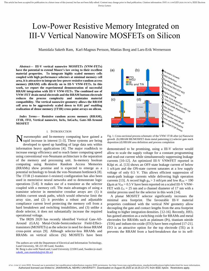
Fig. 1. Cross-sectional process schematic of the VNW 1T1R after (a) Nanowire
growth (b) RRAM BE/MOSFET drain metal patterning (c) selector gate stack deposition (d) RRAM area definition and process completion
Authorized licensed use limited to: JAWAHARLAL NEHRU UNIVERSITY. Downloaded on August 05,2020 at 16:25:13 UTC from IEEE Xplore. Restrictions apply.

0741-3106 (c) 2020 IEEE. Personal use is permitted, but republication/redistribution requires IEEE permission. See http://www.ieee.org/publications_standards/publications/rights/index.html for more information.
This article has been accepted for publication in a future issue of this journal, but has not been fully edited. Content may change prior to final publication. Citation information: DOI 10.1109/LED.2020.3013674, IEEE ElectronDevice Letters
compliance properties and accomplishes low voltage (sub-0.6
V) switching, enabling low-power RRAM operation [22, 23].
The ITO/HfO2 RRAM compatibility with vertical III-V
nanowires was previously demonstrated and operated with an
external VNW selector in series to achieve an endurance of 106
cycles and a retention of 104 seconds measured at 125°C [23].
In this work, we report the successful monolithic co-integration
of ITO/HfO2 based RRAM with III-V vertical transistors
(VNW-FETs) on the same nanowire and demonstrate that the
gate can be used to program the current level within the resistive
element. The compact integration as demonstrated here, not
only provides efficient switching elements, it also provides a
path to reduce parasitic capacitances and resistances to improve
power consumption and speed.
II. DEVICE FABRICATION
The process flow for an integrated III-V VNW-1T1R device is
shown in Fig. 1. First, Metalorganic Vapor Phase Epitaxy
(MOVPE) is used to grow a 300-nm-thick InAs buffer layer on
a p-type Si substrate. Next Au seed particles were patterned
using electron beam lithography (EBL), which are then used to
grow vertical nanowires by the Vapor-Liquid-Solid growth in
MOVPE [24]. The top segment of the nanowire is highly doped
InGaAs. A similar growth sequence with more details has been
reported in [15]. The III-V VNW-FET drain contact that in our
process also acts as the RRAM bottom electrode (BE) is
fabricated next. This is done by first spin coating a 400-nm-
thick hydrogen silsesquioxane (HSQ) film and thickness
definition using EBL. 20-nm-thick Mo is sputtered followed by
15-nm-thick TiN deposited using ALD for the VNW-FET drain
contact and the RRAM BE. Reactive ion etching (RIE) is used
to anisotropically etch the horizontal metal layer on the HSQ so
that it remains only on the vertical nanowire sidewalls. The
HSQ is then removed by a buffered oxide etch (BOE). A SEM
image of the III-V VNW-1T1R after top metal definition is
shown in Fig. 2(a).
The gate length (LG) of the selector III-V VNW-FET is then
defined by EBL as done in the gate-last process for vertical
MOSFETs [25]. In these devices, LG was defined to be 170 nm.
The highly doped shell is etched away using a digital etch
process reducing the NW diameter from 32 nm to 28 nm under
the gate. The gate dielectric deposited using thermal ALD is an
Al2O3/HfO2 bilayer. The thickness of the oxide (tox) is 4 nm that
results in an EOT of 1.5 nm. For the gate metal, first, 2-nm-
thick TiN is deposited using ALD after which 60-nm-thick W
is deposited using sputtering. A SEM image of the device after
gate stack completion is shown in Fig.2 (b). The gate dielectric
that was deposited during thermal ALD is selectively removed
from the top of the wire where the RRAM will be fabricated.
For the RRAM, 2.8 nm HfO2 is deposited using plasma
enhanced ALD (PEALD). The film was grown at an optimized
temperature of 200 using a tetrakis-
ethylmethylaminohafnium (TEMA-Hf) precursor [26]. To
isolate the VNW-MOSFET gate from the RRAM, S1813 resist
spacer is applied and baked at 200. The RRAM cell area is
defined by thinning the resist spacer using oxygen plasma until
~50 nm from the top of the nanowire is exposed. The RRAM
top electrode is finally formed by sputtering 30-nm-thick ITO
and definition using a lift-off process. A cross-sectional SEM
image of the complete integrated device is shown in Fig.2 (c).
III. ELECTRICAL CHARACTERIZATION
The electrical characterization was performed using a Keithley
4200A-SCS. The integrated RRAM forming was carried out by
applying a positive bias (VDS) to the RRAM top electrode (TE).
The bias at the selector gate (VGS) was set to 1.0 V to ensure the
selector is in its ON-state and delivers an ON-state current, ION
= 15 µA. As the RRAM at first is in its high resistive state
(HRS), most of the applied voltage falls across the RRAM
before the conductive filament is formed. We observe that the
forming voltage (VFORM) for the integrated RRAM is ~3.1 V.
The InGaAs segment at the drain segment having a wider
bandgap as compared to the InAs source segment helps to
protect the selector against a breakdown during the forming
process [15, 23]. Once the oxygen vacancy induced filament
was formed, sub-0.5 V RRAM switching was measured that is
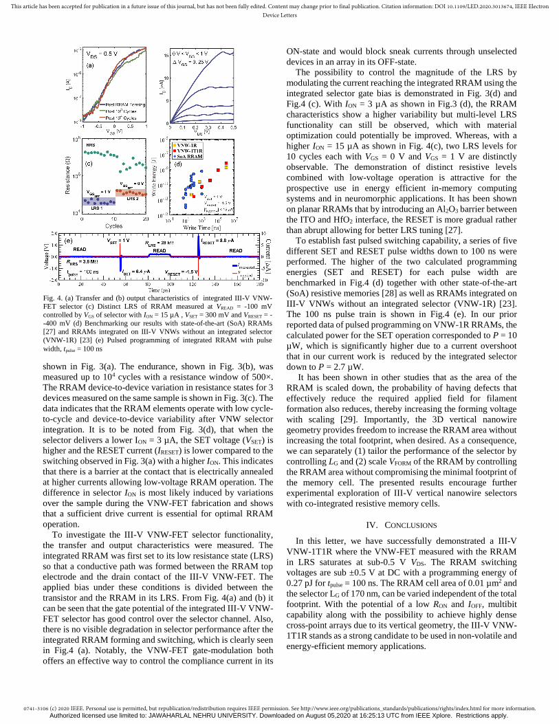
Fig. 3. (a) I-V Switching characteristics with selector ION = 15 µA (b) Endurance measurement up to 104 cycles with VREAD = -100 mV (c) Device-to-device
variability of HRS and LRS between three different devices with VREAD = -100 mV (d) I-V switching characteristics at different VGS of a III-V VNW-FET selector during the SET operation with ION = 3 µA
Fig. 2. SEM images of III-V VNW-1T1R after (a) drain electrode/bottom
electrode deposition (b) selector gate stack deposition and (c) device completion
Authorized licensed use limited to: JAWAHARLAL NEHRU UNIVERSITY. Downloaded on August 05,2020 at 16:25:13 UTC from IEEE Xplore. Restrictions apply.
0741-3106 (c) 2020 IEEE. Personal use is permitted, but republication/redistribution requires IEEE permission. See http://www.ieee.org/publications_standards/publications/rights/index.html for more information.
This article has been accepted for publication in a future issue of this journal, but has not been fully edited. Content may change prior to final publication. Citation information: DOI 10.1109/LED.2020.3013674, IEEE ElectronDevice Letters
shown in Fig. 3(a). The endurance, shown in Fig. 3(b), was
measured up to 104 cycles with a resistance window of 500×.
The RRAM device-to-device variation in resistance states for 3
devices measured on the same sample is shown in Fig. 3(c). The
data indicates that the RRAM elements operate with low cycle-
to-cycle and device-to-device variability after VNW selector
integration. It is to be noted from Fig. 3(d), that when the
selector delivers a lower ION = 3 µA, the SET voltage (VSET) is
higher and the RESET current (IRESET) is lower compared to the
switching observed in Fig. 3(a) with a higher ION. This indicates
that there is a barrier at the contact that is electrically annealed
at higher currents allowing low-voltage RRAM operation. The
difference in selector ION is most likely induced by variations
over the sample during the VNW-FET fabrication and shows
that a sufficient drive current is essential for optimal RRAM
operation.
To investigate the III-V VNW-FET selector functionality,
the transfer and output characteristics were measured. The
integrated RRAM was first set to its low resistance state (LRS)
so that a conductive path was formed between the RRAM top
electrode and the drain contact of the III-V VNW-FET. The
applied bias under these conditions is divided between the
transistor and the RRAM in its LRS. From Fig. 4(a) and (b) it
can be seen that the gate potential of the integrated III-V VNW-
FET selector has good control over the selector channel. Also,
there is no visible degradation in selector performance after the
integrated RRAM forming and switching, which is clearly seen
in Fig.4 (a). Notably, the VNW-FET gate-modulation both
offers an effective way to control the compliance current in its
ON-state and would block sneak currents through unselected
devices in an array in its OFF-state.
The possibility to control the magnitude of the LRS by
modulating the current reaching the integrated RRAM using the
integrated selector gate bias is demonstrated in Fig. 3(d) and
Fig.4 (c). With ION = 3 µA as shown in Fig.3 (d), the RRAM
characteristics show a higher variability but multi-level LRS
functionality can still be observed, which with material
optimization could potentially be improved. Whereas, with a
higher ION = 15 µA as shown in Fig. 4(c), two LRS levels for
10 cycles each with VGS = 0 V and VGS = 1 V are distinctly
observable. The demonstration of distinct resistive levels
combined with low-voltage operation is attractive for the
prospective use in energy efficient in-memory computing
systems and in neuromorphic applications. It has been shown
on planar RRAMs that by introducing an Al2O3 barrier between
the ITO and HfO2 interface, the RESET is more gradual rather
than abrupt allowing for better LRS tuning [27].
To establish fast pulsed switching capability, a series of five
different SET and RESET pulse widths down to 100 ns were
performed. The higher of the two calculated programming
energies (SET and RESET) for each pulse width are
benchmarked in Fig.4 (d) together with other state-of-the-art
(SoA) resistive memories [28] as well as RRAMs integrated on
III-V VNWs without an integrated selector (VNW-1R) [23].
The 100 ns pulse train is shown in Fig.4 (e). In our prior
reported data of pulsed programming on VNW-1R RRAMs, the
calculated power for the SET operation corresponded to P = 10
µW, which is significantly higher due to a current overshoot
that in our current work is reduced by the integrated selector
down to P = 2.7 µW.
It has been shown in other studies that as the area of the
RRAM is scaled down, the probability of having defects that
effectively reduce the required applied field for filament
formation also reduces, thereby increasing the forming voltage
with scaling [29]. Importantly, the 3D vertical nanowire
geometry provides freedom to increase the RRAM area without
increasing the total footprint, when desired. As a consequence,
we can separately (1) tailor the performance of the selector by
controlling LG and (2) scale VFORM of the RRAM by controlling
the RRAM area without compromising the minimal footprint of
the memory cell. The presented results encourage further
experimental exploration of III-V vertical nanowire selectors
with co-integrated resistive memory cells.
IV. CONCLUSIONS
In this letter, we have successfully demonstrated a III-V
VNW-1T1R where the VNW-FET measured with the RRAM
in LRS saturates at sub-0.5 V VDS. The RRAM switching
voltages are sub ±0.5 V at DC with a programming energy of
0.27 pJ for tpulse = 100 ns. The RRAM cell area of 0.01 µm2 and
the selector LG of 170 nm, can be varied independent of the total
footprint. With the potential of a low RON and IOFF, multibit
capability along with the possibility to achieve highly dense
cross-point arrays due to its vertical geometry, the III-V VNW-
1T1R stands as a strong candidate to be used in non-volatile and
energy-efficient memory applications.
Fig. 4. (a) Transfer and (b) output characteristics of integrated III-V VNW-FET selector (c) Distinct LRS of RRAM measured at VREAD = -100 mV
controlled by VGS of selector with ION = 15 µA , VSET = 300 mV and VRESET = -
-400 mV (d) Benchmarking our results with state-of-the-art (SoA) RRAMs
[27] and RRAMs integrated on III-V VNWs without an integrated selector
(VNW-1R) [23] (e) Pulsed programming of integrated RRAM with pulse
width, tpulse = 100 ns
Authorized licensed use limited to: JAWAHARLAL NEHRU UNIVERSITY. Downloaded on August 05,2020 at 16:25:13 UTC from IEEE Xplore. Restrictions apply.

0741-3106 (c) 2020 IEEE. Personal use is permitted, but republication/redistribution requires IEEE permission. See http://www.ieee.org/publications_standards/publications/rights/index.html for more information.
This article has been accepted for publication in a future issue of this journal, but has not been fully edited. Content may change prior to final publication. Citation information: DOI 10.1109/LED.2020.3013674, IEEE ElectronDevice Letters
REFERNCES
[1] J. Hasler and B. Marr, "Finding a roadmap to achieve large
neuromorphic hardware systems", Frontiers in Neuroscience, vol. 7,
2013. doi: 10.3389/fnins.2013.00118. [2] J. J. Yang, D. B. Strukov, and D. R. Stewart, “Memristive devices for
computing,” Nature Nanotechnol., vol. 8, pp. 13–24, Dec. 2012. doi:
10.1038/nnano.2012.240 [3] D. Ielmini and H. S. P. Wong, “In-memory computing with resistive
switching devices,” Nature Electronics, vol. ö1, no. 6, pp. 333–343,
Jun. 2018. doi: 10.1038/s41928-018-0092-2.
[4] L. Danial, E. Pikhay, E. Herbelin, N. Wainstein, V. Gupta, N. Wald,
Y. Roizin, R. Daniel and S. Kvatinsky, "Two-terminal floating-gate
transistors with a low-power memristive operation mode for analogue
neuromorphic computing", Nature Electronics, vol. 2, no. 12, pp. 596-
605, 2019. doi: 10.1038/s41928-019-0331-1.
[5] Z. Wang, S. Joshi, S. Savel’ev, W. Song, R. Midya, Y. Li, M. Rao,
P. Yan, S. Asapu, Y. Zhuo, H. Jiang, P. Lin, C. Li, J. H. Yoon, N.
Upadhyay, J. Zhang, M. Hu, J. P. Strachan, M. Barnell, Q. Wu, H.
Wu, R. S. Williams, Q. Xia & J. J. Yang , "Fully memristive neural
networks for pattern classification with unsupervised learning", Nature
Electronics, vol. 1, no. 2, pp. 137-145, 2018. doi: 10.1038/s41928-018-
0023-2.
[6] Q. Xia and J. Yang, "Memristive crossbar arrays for brain-inspired
computing", Nature Materials, vol. 18, no. 4, pp. 309-323, 2019. Doi:
10.1038/s41563-019-0291-x.
[7] M. Rao, Z. Wang, C. Li, H. Jiang, R. Midya, P. Lin, D. Belkin, W. Song,
S. Asapu, Q. Xia and J. J. Yang, "Learning with Resistive Switching
Neural Networks," 2019 IEEE International Electron Devices Meeting
(IEDM), San Francisco, CA, USA, 2019, pp. 35.4.1-35.4.4. doi:
10.1109/IEDM19573.2019.8993465
[8] W. Shen, P. Huang, M. Fan, R. Han , Z. Zhou , B. Gao , H. Wu , H.
Qian, L. Liu , X. Liu, X. Zhang, and J. Kang, "Stateful Logic Operations
in One-Transistor-One- Resistor Resistive Random Access Memory
Array", IEEE Electron Device Letters, vol. 40, no. 9, pp. 1538-1541,
2019. doi: 10.1109/led.2019.2931947.
[9] International roadmap for devices and systems (IRDS) – More Moore,
(IEEE, pp. 27, 2020)
[10] S. Fujii, R. Ichihara, T. Konno, M. Yamaguchi, H. Seki, H. Tanaka, D.
Zhao, Y. Yoshimura, M. Saitoh, and M. Koyama, "Ag Ionic Memory
Cell Technology for Terabit-Scale High-Density Application," 2019
Symposium on VLSI Technology, Kyoto, Japan, 2019, pp. T188-T189,
doi: 10.23919/VLSIT.2019.8776568.
[11] Q. Luo, X. Xu, H. Liu, H. Lv, T. Gong, S. Long, Q. Liu, H. Sun, W.
Banerjee, L. Li, J. Gao, N. Lua and M. Liu, "Super non-linear RRAM
with ultra-low power for 3D vertical nano-crossbar arrays", Nanoscale,
vol. 8, no. 34, pp. 15629-15636, 2016. doi: 10.1039/c6nr02029a.
[12] Z. Fang, X. P. Wang, X. Li, Z. X. Chen, A. Kamath, G. Q. Lo, and D.
L. Kwong., "Fully CMOS-Compatible 1T1R Integration of Vertical
Nanopillar GAA Transistor and Oxide-Based RRAM Cell for High-
Density Nonvolatile Memory Application", IEEE Transactions on
Electron Devices, vol. 60, no. 3, pp. 1108-1113, 2013. Available:
10.1109/ted.2013.2240389.
[13] O. –P. Kilpi, J. Svensson, E. Lind and L. –E. Wernersson, "Electrical Properties of Vertical InAs/InGaAs Heterostructure MOSFETs", IEEE
Journal of the Electron Devices Society, vol. 7, no. 1, pp. 70-75, 2019.
doi: 10.1109/jeds.2018.2878659.
[14] O. Kilpi, M. Hellenbrand, J. Svensson, A. Persson, R. Lind and L.
Wernersson, "High-Performance Vertical III-V Nanowire MOSFETs
on Si with gm > 3 mS/μm", IEEE Electron Device Letters, pp. 1-1,
2020. Available: 10.1109/led.2020.3004716.
[15] O. -P. Kilpi, J. Svensson, J. Wu, A. Persson, R. Wallenberg, E. Lind
and L. -E. Wernersson, "Vertical InAs/InGaAs Heterostructure Metal–Oxide–Semiconductor Field-Effect Transistors on Si", Nano Letters,
vol. 17, no. 10, pp. 6006-6010, 2017. doi:
10.1021/acs.nanolett.7b02251.
[16] D. Yakimets, G. Eneman, P. Schuddinck, T.H. Bao, M. G. Bardon, P.
Raghavan, A. Veloso, N. Collaert, A. Mercha, D. Verkest, A. Thean,
and Kristin De Meyer, "Vertical GAAFETs for the Ultimate CMOS
Scaling", IEEE Transactions on Electron Devices, vol. 62, no. 5, pp.
1433-1439, 2015. doi: 10.1109/ted.2015.2414924.
[17] A. Singh, S. Blonkowski and M. Kogelschatz, "Resistive switching
study in HfO2 based resistive memories by conductive atomic force microscopy in vacuum", Journal of Applied Physics, vol. 124, no. 1, p.
014501, 2018. doi: 10.1063/1.5025143.
[18] P. Chen, K. Chang, T. Chang, T. Tsai, C. Pan, T. Chu, C. Lin, F. Jin,
M. Chen, H. Huang, M. Wang, I. Lo, J. Zheng and S. Sze, "Bulk
Oxygen–Ion Storage in Indium–Tin–Oxide Electrode for Improved
Performance of HfO2-Based Resistive Random Access Memory", IEEE
Electron Device Letters, vol. 37, no. 3, pp. 280-283, 2016. doi:
10.1109/led.2016.2522085.
[19] W. Banerjee, W. F. Cai, X. Zhao, Q. Liu, H. Lv, S. Longa and Ming
Liu, "Intrinsic anionic rearrangement by extrinsic control: transition of
RS and CRS in thermally elevated TiN/HfO2/Pt RRAM", Nanoscale,
vol. 9, no. 47, pp. 18908-18917, 2017. doi: 10.1039/c7nr06628g.
[20] W. Banerjee and H. Hwang, "Quantized Conduction Device with 6‐Bit
Storage Based on Electrically Controllable Break Junctions", Advanced
Electronic Materials, vol. 5, no. 12, p. 1900744, 2019. doi:
10.1002/aelm.201900744.
[21] W. Banerjee, Q. Liu, H. Hwang, "Engineering of defects in resistive
random access memory devices", Journal of Applied Physics, vol. 127,
no. 5, pp.051101 ,2020, doi: 10.1063/1.5136264
[22] P. Chen, K. Chang, T. Chang, T. Tsai, C. Pan, T. Chu, M. Chen, H.
Huang, I. Lo, J. Zheng, and S. Sze, "Improving Performance by Doping
Gadolinium Into the Indium-Tin–Oxide Electrode in HfO2-Based Resistive Random Access Memory", IEEE Electron Device Letters,
vol. 37, no. 5, pp. 584-587, 2016. doi: 10.1109/led.2016.2548499.
[23] K. -M Persson, M. S. Ram, O. –P. Kilpi, M. Borg and L. –E. Wernersson, "Cross‐Point Arrays with Low‐Power ITO‐HfO2 Resistive
Memory Cells Integrated on Vertical III‐V Nanowires", Advanced
Electronic Materials, vol. 6, no. 6, p. 2000154, 2020. Available: 10.1002/aelm.202000154.
[24] J. Svensson, A. Dey, D. Jacobsson and L. –E. Wernersson, "III–V
Nanowire Complementary Metal–Oxide Semiconductor Transistors Monolithically Integrated on Si", Nano Letters, vol. 15, no. 12, pp.
7898-7904, 2015. doi: 10.1021/acs.nanolett.5b02936.
[25] M. Berg, O. -P. Kilpi, K. -M. Persson, J. Svensson, M. Hellenbrand, E.
Lind, and L.-E. Wernersson., "Electrical Characterization and
Modeling of Gate-Last Vertical InAs Nanowire MOSFETs on
Si", IEEE Electron Device Letters, vol. 37, no. 8, pp. 966-969, 2016.
doi: 10.1109/led.2016.2581918.
[26] K. –M. Persson, M. S. Ram, M. Borg and L. –E. Wernersson, "Investigation of Reverse Filament Formation in ITO/HfO2-based
RRAM," 2019 Device Research Conference (DRC), Ann Arbor, MI,
USA, 2019, pp. 91-92. doi: 10.1109/DRC46940.2019.9046443. [27] C.Mahata, C. Lee, Y. An, M. -H. Kim, S. Bang, C. S. Kim, Ji. –H. Ryu,
S. Kim, H. Kim, B. –G. Park, "Resistive switching and synaptic behaviors of an HfO2/Al2O3 stack on ITO for neuromorphic systems",
Journal of Alloys and Compounds, vol. 826, p. 154434, 2020.
Available: 10.1016/j.jallcom.2020.154434. [28] H.-S. P. Wong, C. Ahn, J. Cao, H.-Y. Chen, S. B. Eryilmaz, S. W. Fong,
J. A. Incorvia, Z. Jiang, H. Li, C. Neumann, K. Okabe, S. Qin, J. Sohn,
Y. Wu, S. Yu, X. Zheng, “Stanford Memory Trends,” https://nano.stanford.edu/stanford-memory-trends, accessed June 25,
2020.
[29] A. Chen, "Area and Thickness Scaling of Forming Voltage of Resistive Switching Memories", IEEE Electron Device Letters, vol. 35, no. 1, pp.
57-59, 2014. doi: 10.1109/led.2013.2288262.
Authorized licensed use limited to: JAWAHARLAL NEHRU UNIVERSITY. Downloaded on August 05,2020 at 16:25:13 UTC from IEEE Xplore. Restrictions apply.