Embed Size (px)
Citation preview

Information Processing Letters 23 (1986) 5-9 North-Holland
20 July 1986
LONG EDGES IN THE LA YOUTS OF SHUFFLE-EXCHANGE AND CUBE-CONNECTED
CYCLES GRAPHS
Ferng-Ching LIN and Wei-Kuan SHIH
Department of Computer Science and Information Engineering, College of Engineering, National Taiwan Unioersity, Taipei, Taiwan, Republic of China
Communicated by K. Mehlhorn Received March 1985 Revised 4 September 1985
A direct method is devised to prove, without information-theoretic arguments, the ~(N2/log2N) wire area lower bound for the shuffle-exchange and cube-connected cycles graphs. We further show the high occurrence of long edges in two ways: (1) In any layout, there are f~(N/log N) edges whose lengths are at least N/32 log2N. (2) The edges whose lengths are at least N/64 log2N occupy fi(N2/log2N) wire area.
Keywords: Graph layout, wire area, long edges, lower bound, shuffle-exchange, cube-connected cycles, path-edge, communica- tion power of edge, VLSI
1. Introduction
In VLSI computat ion, if a solution to some problem is in the form of a communica t ion graph of processors, an efficient layout is desired to implement the graph. Minirni7.irtg wire area is a critical concern due to the fact that layouts con- suming a larger amount of chip area are more expensive to fabricate and less reliable. Speed of course is another critical factor in chip perfor- mance. Long wires raise propagat ion delays which can slow down the clock and hence reduce the throughput of the system. These are two of the major VLSI layout problems which have stimu- lated considerable interest in theoretical study [1].
For the formal model of VLSI graph layouts, we shall adopt the simple and widely accepted grid model [6,7]. Layouts are assumed to be on rectangular grids formed by horizontal and verti- cal grid lines which are spaced apart by unit intervals. The nodes of a graph are located only at the intersections of grid l ines - - the grid points. Edges are routed as wires through the grid lines to
connect nodes. Any two edges are not allowed to overlap for any distance, and an edge cannot overlap any node which is not an end-node of that edge. The layout area is defined to be the number of all grid points in the grid. The wire area, however, is the count of those grid points covered by the edges.
The shuffle-exchange [5] and cube-connected cycles [4] graphs are two pre-eminent structures for parallel computa t ion because of their eco- nomic interconnection patterns. In them, the hardware cost and efficiency are traded off in search of the best compromise for a contemplated range of applications. Thompson [6] first showed that any layout of a graph which computes an N-poin t Fourier t ransform in T steps requires f~(N2/T 2) chip area. This implies that any layout of the N-node shuffle-exchange or cube-connected cycles graph requires f~(N2/log2N) chip area. For the proofs, see also [7]. Leighton [3] then proved an analogous but stronger lower bound statement for the wire area. He also proved that any graph which computes an N-point Fourier transform
0020-0190/86/$3.50 © 1986, Elsevier Science Publishers B.V. (North-Holland) 5

Volume 23, Number 1 INFORMATION PROCESSING LE'Iq'ERS 20 July 1986
must have a wire which crosses f i ( N / T 2) other wires. This, in particular, means that any layout of the N-node shuffle-exchange or cube-connected cycles graph contains a wire of f~(N/log2N) length.
All the lower bound results mentioned above are indirectly derived through information-theo- retic (area-time tradeoff) arguments. In this paper, we shall devise a method to prove these lower bounds directly. The basic idea is roughly as fol- lows. If we separate some or all of the nodes of the graph into two parts, between them there must be at least a certain amount of communicating paths. According to the interconnection pattern of the graph, removing one edge can only destroy some communicating paths, hence there must be at least a certain number of edges connecting these two parts. By using this kind of information, we are not only able to derive wire area lower bounds but also lower bounds on the number of long edges. In fact, we strengthen Leighton's result by showing that there are f~(N/log N) edges which are at least N / 3 2 log2N long. Furthermore, we show that the wire area occupied by the edges whose lengths are at least N / 6 4 log2N is as large (up to a constant) as the whole wire area.
2. Communication power of edges
In order to extract the communication ability of a given graph, we shall consider 'path-edges' which are paths properly selected from the origi- nal graph. The concept of 'path-edge' will become explicit when we deal with those two particular graphs in the next section. We need a few defini- tions for describing the communication power of edges. 'Edges' used in this section really are 'path-edges' when applied to concrete examples in the next section.
Definition 2.1. The diameter D of a given graph is the smallest integer such that, for any two nodes i and j, i can be connected to j in at most D steps.
Definition 2.2. Let e be any edge, 1 ~< d ~< D, 1 ~< h d. A communication circle can be defined as the
set of node pairs
C(e, d, h ) = { (i, j ) l i and j are nodes such that there is a d-step path from i to j, with e as the hth step in the path}.
Definition 2.3. If e is an edge, we define the pairing set of e as
P(e) = {(i, j)Ji and j are nodes such that there is a path from i to j through e and the number of steps in the path is at most D}.
To serve our purpose, we should constrain the graphs to be of bounded degree. In this paper, we are only interested in the case that the in-degree and out-degree of each node are bounded by 2, although the results obtained here can be ex- tended naturally. The following easy lemma can be used to bound from above the size of com- munication circles and pairing sets.
Lemma 2.4. I f the diameter is D and the degree bound is 2, then, for any e, 1 ~< d ~< D, 1 ~< h ~< d,
(a) I C(e, d, h) I ~< 2 a- 1, (b) I P(e) I ~ D(2 D - 1).
Proof. (a) In C(e, d, h), let m count the starting nodes with multiplicity and n count the ending nodes with multiplicity. It is clear that m ~< 2 h-1 and n ~< 2 d- h. So,
IC(e, d, h) l ~ m n ~ 2h-12 d - h = 2 d-1.
(b) Since
a ( e ) = [,.J C(e, d, h), l < d ~ < D , l < h < d
we have
D D
IP(e) I ~< E d2d-a ~< D E 2d-a d = l d = l
~< D(2D-- 1). []
If we purposely choose a set of nodes S to be observed, we can define the communication power of an edge relative to that set as the number of communicating pairs through that edge with both starting and ending nodes in S. Also, the diameter,
Volume 23, Number 1 INFORMATION PROCESSING LETTERS 20 July 1986
if necessary, should be reduced to fit the situation of the set of observed nodes.
i ° 2P %1
Definition 2.5. Suppose S is a set of observed nodes and e is any edge in the graph. We define the communicat ion power of e relative to S as
Ps(e) = { (i, j ) l i , j ~ S and (i, j) ~ P(e) },
and define
R s = max IPs(e)I. e
3. Shuffle-exchange and cube-connected cycles
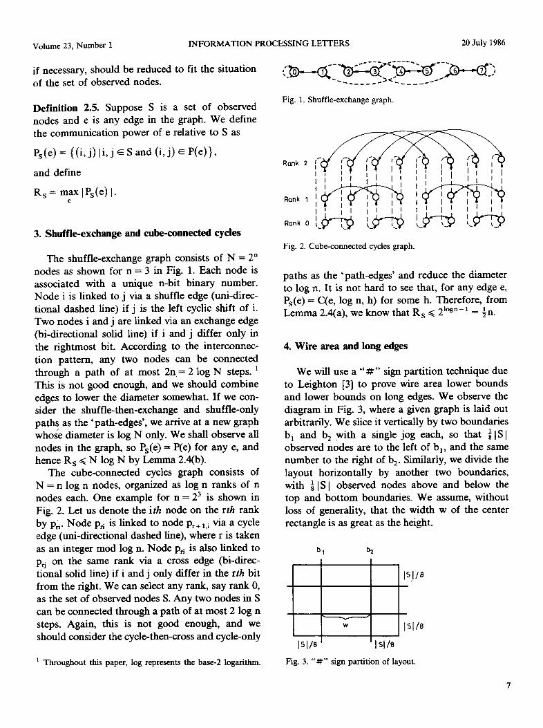
The shuffle-exchange graph consists of N = 2" nodes as shown for n = 3 in Fig. 1. Each node is associated with a unique n-bit binary number. Node i is linked to j via a shuffle edge (uni-direc- tional dashed line) if j is the left cyclic shift of i. Two nodes i and j are linked via an exchange edge (bi-directional solid line) if i and j differ only in the rightmost bit. According to the interconnec- tion pattern, any two nodes can be connected through a path of at most 2n = 2 log N steps. ] This is not good enough, and we should combine edges to lower the diameter somewhat. If we con- sider the shuffle-then-exchange and shuffle-only paths as the 'path-edges' , we arrive at a new graph whose diameter is log N only. We shall observe all nodes in the graph, so Ps(e) = P(e) for any e, and hence R s ~< N log N by Lemma 2.4(b).
The cube-connected cycles graph consists of N = n log n nodes, organized as log n ranks of n nodes each. One example for n = 2 3 is shown in Fig. 2. Let us denote the ith node on the rth rank by p~. Node P~i is linked to node Pr+l,i via a cycle edge (uni-directional dashed line), where r is taken as an integer mod log n. Node p,~ is also l inked to po on the same rank via a cross edge (bi-direc- tional solid line) if i and j only differ in the rth bit from the right. We can select any rank, say rank 0, as the set of observed nodes S. Any two nodes in S can be connected through a path of at most 2 log n steps. Again, this is not good enough, and we should consider the cycle-then-cross and cycle-only
Fig. 1. Shuffle-exchange graph.
Rank 2
Rank I
Rank 0
, ' ! ' ' I I I t ' i ' ~ - " L > . , ~ ' - ~ - ~ I I ' , _ . . - ~ ~ ~
"{ i " r ~'!" I t I ] I ~ I ~, I ~, I ' , I I I I I I d I I I ~ , i . L . - - i ~ , ~ l,..k-'-~..k ~ 2 . r - r % L ~ L~ ) L V ~ V L Y LY L Y ~
Fig. 2. Cube-connected cycles graph.
paths as the 'path-edges ' and reduce the diameter to log n. It is not hard to see that, for any edge e, Ps(e) = C(e, log n, h) for some h. Therefore, from Lemma 2.4(a), we know that R s < 2 l°g"-I = ½n.
4. Wire area and long edges
We will use a " # " sign part i t ion technique due to Leighton [3] to prove wire area lower bounds and lower bounds on long edges. We observe the diagram in Fig. 3, where a given graph is laid out arbitrarily. We slice it vertically by two boundaries b 1 and b 2 with a single jog each, so that {ISI observed nodes are to the left of b a, and the same number to the right of b 2. Similarly, we divide the layout horizontally by another two boundaries, with ~ I SI observed nodes above and below the top and bo t tom boundaries. We assume, without loss of generality, that the width w of the center rectangle is as great as the height.
b, b
W
Isl18 Isl lB
IS l18
h
Is l /8
1 Throughout this paper, log represents the base-2 logarithm. Fig. 3. " # " sign partition of layout.

Volume 23, Number 1 INFORMATION PROCESSING LETTERS 20 July 1986
Lemma 4.1. w >~ IS 12/32Rs •
Proof. The number of observed nodes in the center rectangle is at least ½1S [, and there are at least ¼ I SI in the rest area. So, there are at least 1_ 21SI ×¼1S1=11SI 2 node pairs across the pe- rimeter of the center rectangle. By the definition of R s we know that the perimeter should cut at least IS I2/8Rs edges. Hence,
4w>t I S I2 /8Rs or w>~ I SI2 /32Rs • []
Lemma 4.2. The wire area of any layout is ~2( I SI 4/R%).
Proof. Any vertical boundary between bl and b2 must cut at least (I IS I × -~ IS [ ) /Rs = IS 12/64Rs edges. Consequently, the occupied wire area be- tween b~ and b 2 is at least
w( IS [ 2/64Rs) = IS 14/(32 x 64R2). []
at least one edge whose length is at least w /D . But such an edge can communicate at most R s node pairs. We thus conclude that there are at least (-~ IS I × ~ IS I ) /Rs = IS [ 2/64Rs edges whose lengths are at least w / D . []
Theorem 4.5. Any layout of N-node shuffle-ex- change or cube-connected cycles graph contains f~(N/ logN) edges whose lengths are at least N / 3 2 log2N.
Proof. The proof immediately follows from Lem- mas 4.1 and 4.4. []
For both graphs, if we take the sum of the lengths of the long edges, we find that the wire area occupied by the long edges is fl(n2/log3N), which is slightly smaller than the lower bound of the Whole wire area by a factor of log N. Nonethe- less, we can match up these two bounds by consid- ering half-long edges also.
Theorem 4.3. Any layout of the N-node shuffle-ex- change or cube-connected cycles graph occupies ~2 (N 2/log 2 N) wire area.
Lemma 4.6. In any layout, the wire area occupied by the edges whose lengths are at least w / 2 D is f~( IS 14/REs).
Proof. For the shuffle-exchange graph, as dis- cussed in the previous section, we have R s N log N, where IS I = N. By Lemma 4.2, we get the desired wire area lower bound. For the cube-connected cycles graph, IS1 = n and R s
½n, therefore the wire area, by Lemma 4.2, is f~(n2), i.e., f~(N2/log2N). []
As regards Fig. 3 again, an observed node left to ba can be connected to any observed node right t o b E by a path whose length is at least w. The average edge length in the path is at least w / D if the number of steps is not greater than D. So we are sure that there must be one edge in the path whose length is at least w / D . Such an edge is considered to be long.
Lemma 4.4. In any layout, there are (ISI2/Rs) edges whose lengths are at least w / D .
Proof. In any path connecting an observed node left to b 1 to an observed node right to b2, there is
Proof. Use the same layout partition as before. In any path connecting an observed node left to b 1 and an observed node right to b 2, if the total length of the path is L (>~ w) and there are y (< D) edges whose lengths are less than w/2D, then the length sum of the edges whose lengths are at least
w / 2 D >/L - yw/2D >i L - y L / 2 D
= L ( D + ( D - y)/2D)>~½L.
Recall that in the proof of Lemma 4.2 we estimate the whole wire area (= 2(IS 14/R%)) by this kind of paths. Since at least half of the length of these paths is occupied by those long and half-long edges, we have proven the lemma. []
Theorem 4.7. In any layout of N-node shuffle-ex- change or cube-connected cycles graph, the wire area occupied by the edges whose lengths are at least N / 6 4 logZN is ~(N2/log2N).
Volume 23, Number 1 INFORMATION PROCESSING LETI'ERS 20 July 1986
5. Concluding remarks
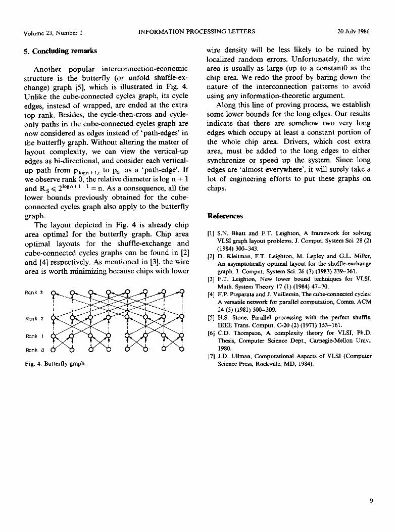
Another popular interconnection-economic structure is the butterfly (or unfold shuffle-ex- change) graph [5], which is illustrated in Fig. 4. Unlike the cube-connected cycles graph, its cycle edges, instead of wrapped, are ended at the extra top rank. Besides, the cycle-then-cross and cycle- only paths in the cube-connected cycles graph are now considered as edges instead of 'path-edges' in the butterfly graph. Without altering the matter of layout complexity, we can view the vertical-up edges as bi-directional, and consider each vertical- up path from Plogn+l,i to P0i as a 'path-edge'. If we observe rank 0, the relative diameter is log n + 1 and R s ~< 2 l°gn+1-1 = n. As a consequence, all the lower bounds previously obtained for the cube- connected cycles graph also apply to the butterfly graph.
The layout depicted in Fig. 4 is already chip area optimal for the butterfly graph. Chip area optimal layouts for the shuffle-exchange and cube-connected cycles graphs can be found in [2] and [4] respectively. As mentioned in [3], the wire area is worth minimizing because chips with lower
Ran k 3
Ronk 2
Ronk I
Rank 0
Fig. 4. Butterfly graph.
wire density will be less likely to be ruined by localized random errors. Unfortunately, the wire area is usually as large (up to a constant0 as the chip area. We redo the proof by baring down the nature of the interconnection patterns to avoid using any information-theoretic argument.
Along this line of proving process, we establish some lower bounds for the long edges. Our results indicate that there are somehow two very long edges which occupy at least a constant portion of the whole chip area. Drivers, which cost extra area, must be added to the long edges to either synchronize or speed up the system. Since long edges are 'almost everywhere', it will surely take a lot of engineering efforts to put these graphs on chips.
References
[1] S.N. Bhatt and F.T. Leighton, A framework for solving VLSI graph layout problems, J. Comput. System Sci. 28 (2) (1984) 300-343.
[2] D. Kleitman, F.T. Leighton, M. Lepley and G.L. Miller, An asymptotically optimal layout for the shuffle-exchange graph, J. Comput. System Sci. 26 (3) (1983) 339-361.
[3] F.T. Leighton, New lower bound techniques for VLSI, Math. System Thex)ry 17 (1) (1984) 47-70.
[4] F.P. Preparata and J. VuiUemin, The cube-connected cycles: A versatile network for parallel computation, Comm. ACM 24 (5) (1981) 300-309.
[5] H.S. Stone, Parallel processing with the perfect shuffle, IEEE Trans. Comput. C-20 (2) (1971) 153-161.
[6] C.D. Thompson, A complexity theory for VLSI, Ph.D. Thesis, Computer Science Dept., Carnegie-Mellon Univ., 1980.
[7] J.D. Ullman, Computational Aspects of VLSI (Computer Science Press, Rockville, MD, 1984).
9