Embed Size (px)
Citation preview

LogiCORE IP AXI to APB Bridge (v1.01.a)
Product Guide
PG073 July 25, 2012

AXI to APB Bridge v1.01.a www.xilinx.com 2PG073 July 25, 2012
Table of ContentsIP Facts
Chapter 1: OverviewFeature Summary. . . . . . . . . . . . . . . . . . . . . . . . . . . . . . . . . . . . . . . . . . . . . . . . . . . . . . . . . . . . . . . . . . 5Unsupported Features. . . . . . . . . . . . . . . . . . . . . . . . . . . . . . . . . . . . . . . . . . . . . . . . . . . . . . . . . . . . . . 5Licensing and Ordering Information . . . . . . . . . . . . . . . . . . . . . . . . . . . . . . . . . . . . . . . . . . . . . . . . . . . 6
Chapter 2: Product SpecificationStandards Compliance . . . . . . . . . . . . . . . . . . . . . . . . . . . . . . . . . . . . . . . . . . . . . . . . . . . . . . . . . . . . . . 8Performance. . . . . . . . . . . . . . . . . . . . . . . . . . . . . . . . . . . . . . . . . . . . . . . . . . . . . . . . . . . . . . . . . . . . . . 8Resource Utilization and Maximum Frequencies . . . . . . . . . . . . . . . . . . . . . . . . . . . . . . . . . . . . . . . . 8Port Descriptions . . . . . . . . . . . . . . . . . . . . . . . . . . . . . . . . . . . . . . . . . . . . . . . . . . . . . . . . . . . . . . . . . 11Register Descriptions . . . . . . . . . . . . . . . . . . . . . . . . . . . . . . . . . . . . . . . . . . . . . . . . . . . . . . . . . . . . . . 14
Chapter 3: Designing with the CoreGeneral Design Guidelines . . . . . . . . . . . . . . . . . . . . . . . . . . . . . . . . . . . . . . . . . . . . . . . . . . . . . . . . . 15Clocking. . . . . . . . . . . . . . . . . . . . . . . . . . . . . . . . . . . . . . . . . . . . . . . . . . . . . . . . . . . . . . . . . . . . . . . . . 20Resets . . . . . . . . . . . . . . . . . . . . . . . . . . . . . . . . . . . . . . . . . . . . . . . . . . . . . . . . . . . . . . . . . . . . . . . . . . 20Timing Diagrams . . . . . . . . . . . . . . . . . . . . . . . . . . . . . . . . . . . . . . . . . . . . . . . . . . . . . . . . . . . . . . . . . 20
Chapter 4: Customizing and Generating the CoreGUI . . . . . . . . . . . . . . . . . . . . . . . . . . . . . . . . . . . . . . . . . . . . . . . . . . . . . . . . . . . . . . . . . . . . . . . . . . . . 22
Appendix A: Migrating
Appendix B: Debugging

AXI to APB Bridge v1.01.a www.xilinx.com 3PG073 July 25, 2012
Appendix C: Additional ResourcesXilinx Resources . . . . . . . . . . . . . . . . . . . . . . . . . . . . . . . . . . . . . . . . . . . . . . . . . . . . . . . . . . . . . . . . . . 26Solution Centers. . . . . . . . . . . . . . . . . . . . . . . . . . . . . . . . . . . . . . . . . . . . . . . . . . . . . . . . . . . . . . . . . . 26References . . . . . . . . . . . . . . . . . . . . . . . . . . . . . . . . . . . . . . . . . . . . . . . . . . . . . . . . . . . . . . . . . . . . . . 26Technical Support . . . . . . . . . . . . . . . . . . . . . . . . . . . . . . . . . . . . . . . . . . . . . . . . . . . . . . . . . . . . . . . . 27Revision History . . . . . . . . . . . . . . . . . . . . . . . . . . . . . . . . . . . . . . . . . . . . . . . . . . . . . . . . . . . . . . . . . . 27Notice of Disclaimer. . . . . . . . . . . . . . . . . . . . . . . . . . . . . . . . . . . . . . . . . . . . . . . . . . . . . . . . . . . . . . . 27

AXI to APB Bridge v1.01.a www.xilinx.com 4PG073 July 25, 2012 Product Specification
IntroductionThe Advanced Microcontroller Bus Architecture (AMBA®) Advanced eXtensible Interface (AXI) to Advanced Peripheral Bus (APB) Bridge translates AXI4-Lite transactions into APB transactions. It functions as a slave on the AXI4-Lite interface and as a master on the APB interface. The AXI to APB Bridge main use model is to connect the APB slaves with AXI masters.
FeaturesThe Xilinx AXI to APB Bridge is a soft IP core with these features:
• AXI interface is based on the AXI4-Lite specif ication
• APB interface is based on the APB3 specif ication, supports optional APB4 selection
• Supports 1:1 (AXI:APB) synchronous clock ratio
• Connects as a 32-bit slave on 32-bit AXI4-Lite interface
• Connects as a 32-bit master on 32-bit APB3/APB4 interface
• Supports optional data phase time out
IP Facts
LogiCORE IP Facts Table
Core Specifics
Supported Device Family(1)
Zynq™-7000(2), Virtex®-7(3), Kintex™-7(3),Artix™-7(3), Virtex-6(4), Spartan®-6(5)
Supported User Interfaces AXI4-Lite, APB3, APB4
Resources See Table 2-1. through Table 2-5
Provided with CoreDesign Files VHDL
Example Design Not Provided
Test Bench Not Provided
Constraints File None
Simulation Model None
Supported S/W Driver
N/A
Tested Design Flows(6)
Design EntryXilinx Platform Studio (XPS)
Vivado Design Suite v2012.2(7)
Simulation Mentor Graphics ModelSim
SynthesisXilinx Synthesis Technology (XST)
Vivado Synthesis
SupportProvided by Xilinx @ www.xilinx.com/support
Notes: 1. For a complete list of supported derivative devices, see
Embedded Edition Derivative Device Support.2. Supported in ISE Design Suite implementations only.
3. For more information, see 7 Series FPGAs Overview [Ref 3].
4. For more information, see Virtex-6 Family Overview [Ref 3].5. For more information, see Spartan-6 Family Overview [Ref 3].6. For the supported versions of the tools, see the Xilinx Design
Tools: Release Notes Guide.7. Supports only 7 series devices.

AXI to APB Bridge v1.01.a www.xilinx.com 5PG073 July 25, 2012
Chapter 1
OverviewThe main function of the LogiCORE™ IP Advanced eXtensible Interface (AXI) to Advanced Peripheral Bus (APB) Bridge core is to connect APB slaves to AXI masters. It translates AXI4-Lite transactions into APB transactions.
This chapter contains these sections:
• Feature Summary
• Unsupported Features
• Licensing and Ordering Information
Feature SummaryThe 32-bit AXI4-Lite interface on the AXI to APB Bridge core is based on the AMBA AXI and ACE Protocol Specification v2.0 [Ref 1]. The core functions as a 32-bit slave on this interface.
The core’s 32-bit APB interface is based on the AP3 interface as described in the AMBA APB Protocol Specification v2.0 [Ref 1]. The core supports the optional APB4 interface as well. The core functions as a 32-bit master on the APB3/APB4 interface.
The AXI to APB Bridge core supports a 1:1 (AXI:APB) synchronous clock ratio as well as data phase timeout.
Unsupported Features
AXI4-Lite Slave InterfaceThese features are not supported in the AXI to APB Bridge core:
• 64-bit width is not supported
• When write and read transfers are both requested, the read request, which has higher priority, is accepted f irst.

AXI to APB Bridge v1.01.a www.xilinx.com 6PG073 July 25, 2012
Licensing and Ordering Information
Licensing and Ordering InformationThis Xilinx LogiCORE IP module is provided at no additional cost with the Xilinx Vivado Design Suite and ISE Design Suite Embedded Edition tools under the terms of the Xilinx End User License.
Information about this and other Xilinx LogiCORE IP modules is available at the Xilinx Intellectual Property page. For information on pricing and availability of other Xilinx LogiCORE IP modules and tools, contact your local Xilinx sales representative.

AXI to APB Bridge v1.01.a www.xilinx.com 7PG073 July 25, 2012 Product Specification
Chapter 2
Product SpecificationThe AXI to APB Bridge translates AXI4-Lite transactions into APB transactions. The bridge functions as a slave on the AXI4-Lite interface and as a master on the APB interface.
The AXI to APB Bridge block diagram, shown in Figure 2-1, is described in subsequent sections.
AXI4-Lite Slave Interface
The AXI4-Lite Slave Interface module provides a bidirectional slave interface to the AXI. The AXI address and data bus widths are always fixed to 32 bits. When both write and read transfers are simultaneously requested on AXI4-Lite, the read request is given more priority than the write request. This module also contains the data phase time out logic for generating an OK response on the AXI interface when an APB slave does not respond.
APB Master Interface
The APB Master module provides the APB master interface on the APB. This interface can be APB3 or APB4, which can be selected by setting the generic C_M_APB_PROTOCOL. When C_M_APB_PROTOCOL=apb4, the M_APB_PSTRB and M_APB_PPROT signals are driven at the APB interface. The APB address and data bus widths are f ixed to 32 bits.
X-Ref Target - Figure 2-1
Figure 2-1: AXI to APB Bridge Block Diagram
AXI4-LiteSlave
Interface
APB Master
Interface
AXI4-Lite APB3/APB4
DS788_01

AXI to APB Bridge v1.01.a www.xilinx.com 8PG073 July 25, 2012 Product Specification
Standards Compliance
Standards ComplianceThe AXI to APB Bridge core is based on the AMBA® AXI4-Lite specif ication and the APB3/APB4 specification.
PerformanceThis section details the performance information for various core configurations.
LatencyThe core is configured for the best possible configuration for calculating read latency. The read latency from read address valid (S_AXI_ARVALID) to the data beat (S_AXI_RVALID) of AXI to APB Bridge is three clock cycles.
Resource Utilization and Maximum FrequenciesBecause the AXI to APB Bridge module used with other design pieces in the FPGA, the resource utilization and timing numbers reported in this section are estimates only. When the AXI to APB Bridge is combined with other pieces of the FPGA design, the utilization of FPGA resources and timing of the design varies from the results reported here.
The AXI to APB Bridge resource utilization benchmarks for a variety of parameter combinations measured with Virtex-6 FPGA as the target device using the ISE® tool are shown in Table 2-1.
Table 2-1: Performance and Resource Utilization Benchmarks on the Virtex-6 FPGA (xc6vlx130t-ff1156-1)
Parameter Values (other parameters at default value) Device Resources Performance
C_A
PB_N
UM
_SL
AVES
C_M
_APB
_PRO
TOCO
L
C_D
PHA
SE_T
IMEO
UT
Slic
es
Slic
e Fl
ip-F
lops
LUTs
F MA
X (M
Hz)
1 apb3 0 30 146 120 200
1 apb3 16 39 152 153 200
1 apb4 256 49 167 160 200

AXI to APB Bridge v1.01.a www.xilinx.com 9PG073 July 25, 2012 Product Specification
Resource Utilization and Maximum Frequencies
The AXI to APB Bridge resource utilization benchmarks for a variety of parameter combinations measured with Spartan-6 FPGA as the target device using the ISE tool are shown in Table 2-2.
The AXI to APB Bridge resource utilization benchmarks for a variety of parameter combinations measured with Virtex-7 FPGA as the target device using the ISE tool are shown in Table 2-3.
Table 2-2: Performance and Resource Utilization Benchmarks on the Spartan-6 FPGA (xc6slx100t-fgg900-2)
Parameter Values (other parameters at default value) Device Resources Performance
C_A
PB_N
UM
_SL
AVES
C_M
_APB
_PRO
TOCO
L
C_D
PHA
SE_T
IMEO
UT
Slic
es
Slic
e F
lip-F
lops
LUT
s
FM
AX (
MH
z)
1 apb3 0 40 146 138 150
1 apb3 16 47 152 158 150
1 apb4 256 52 168 164 150
Table 2-3: Performance and Resource Utilization Benchmarks on the Virtex-7 FPGA (xc7v855tffg1157-3)
Parameter Values (other parameters at default value) Device Resources Performance
C_A
PB_N
UM
_SL
AVES
C_M
_APB
_PRO
TOCO
L
C_D
PHA
SE_T
IMEO
UT
Slic
es
Slic
e Fl
ip-F
lops
LUTs
F MA
X (M
Hz)
1 apb3 0 35 145 133 200
1 apb3 16 39 151 143 200
1 apb4 256 44 166 169 200
AXI to APB Bridge v1.01.a www.xilinx.com 10PG073 July 25, 2012 Product Specification
Resource Utilization and Maximum Frequencies
The AXI to APB Bridge resource utilization benchmarks for a variety of parameter combinations measured with an Artix-7 FPGA as the target device using the ISE tool are shown in Table 2-4.
The AXI to APB Bridge resource utilization benchmarks for a variety of parameter combinations measured with a Kintex-7 FPGA as the target device using the ISE tool are shown in Table 2-5.
Table 2-4: Performance and Resource Utilization Benchmarks on the Artix-7 and Zynq-7000 [Artix-7 Based Fabric] Devices (xc7a350tfbg676-3)
Parameter Values (other parameters at default value) Device Resources Performance
C_A
PB_N
UM
_SL
AVES
C_M
_APB
_PRO
TOCO
L
C_D
PHA
SE_T
IMEO
UT
Slic
es
Slic
e Fl
ip-F
lops
LUTs
F MA
X (M
Hz)
1 apb3 0 36 145 135 200
1 apb3 16 40 151 153 200
1 apb4 256 41 165 154 200
Table 2-5: Performance and Resource Utilization Benchmarks on the Kintex-7 and Zynq-7000 [Kintex-7 Based Fabric] FPGA (xc7k410tffg676-3)
Parameter Values (other parameters at default value) Device Resources Performance
C_A
PB_N
UM
_SL
AVES
C_M
_APB
_PRO
TOCO
L
C_D
PHA
SE_T
IMEO
UT
Slic
es
Slic
e Fl
ip-F
lops
LUTs
F MA
X (M
Hz)
1 apb3 0 34 145 133 200
1 apb3 16 38 151 143 200
1 apb4 256 43 166 169 200
AXI to APB Bridge v1.01.a www.xilinx.com 11PG073 July 25, 2012 Product Specification
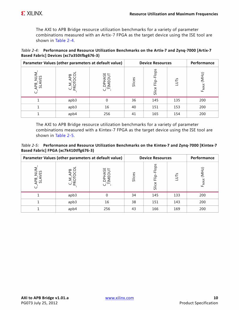
Port Descriptions
Port DescriptionsTable 2-6 shows the I/O signals of the AXI to APB Bridge.
Table 2-6: I/O Signal Description
Port Signal Name Interface I/O Initial State Description
AXI Interface System Signals
P1 S_AXI_ACLK System I - AXI clock
P2 S_AXI_ARESETN System I - AXI reset, active low
AXI Write Address Channel Signals
P3 S_AXI_AWADDR[C_S_AXI_ADDR_WIDTH-1:0] AXI4-Lite I -
AXI Write address. The write address bus gives the address of the f irst transfer in a write burst transaction
P4 S_AXI_AWPROT[2:0](1) AXI4-Lite I -
Protection type. This signal indicates the normal, privileged, or secure protection level of the write transaction and whether the transaction is a data access or an instruction access. The default value is normal non secure data access
P5 S_AXI_AWVALID AXI4-Lite I -Write address valid. This signal indicates that valid write address and control information are available
P6 S_AXI_AWREADY AXI4-Lite O 0Write address ready. This signal indicates that the slave is ready to accept an address and associated control signals
AXI Write Data Channel Signals
P7 S_AXI_WDATA[C_S_AXI_DATA_WIDTH-1:0] AXI4-Lite I - Write data bus
P8 S_AXI_WSTB[C_S_AXI_DATA_WIDTH/8-1:0](1) AXI4-Lite I - Write strobes. This signal indicates which
byte lanes to update in memory
P10 S_AXI_WVALID AXI4-Lite I - Write valid. This signal indicates that valid write data and strobes are available
P11 S_AXI_WREADY AXI4-Lite O 0 Write ready. This signal indicates that the slave can accept the write data
AXI Write Response Channel Signals
P12 S_AXI_BRESP[1:0] AXI4-Lite O 0 Write response. This signal indicates the status of the write transaction
P13 S_AXI_BVALID AXI4-Lite O 0 Write response valid. This signal indicates that a valid write response is available
P14 S_AXI_BREADY AXI4-Lite I - Response ready. This signal indicates that the master can accept the response information

AXI to APB Bridge v1.01.a www.xilinx.com 12PG073 July 25, 2012 Product Specification
Port Descriptions
AXI Read Address Channel Signals
P15 S_AXI_ARADDR[C_S_AXI_ADDR_WIDTH -1:0] AXI4-Lite I - Read address. The read address bus gives the
initial address of a read burst transaction
P16 S_AXI_ARPROT[2:0](1) AXI4-Lite I -
Protection type. This signal provides protection unit information for the read transaction. The default value is normal non secure data access
P17 S_AXI_ARVALID AXI4-Lite I -
Read address valid. When High, this signal indicates that the read address and control information is valid and remains stable until the address acknowledgement signal, S_AXI_ARREDY, is High.
P18 S_AXI_ARREADY AXI4-Lite O 0Read address ready. This signal indicates that the slave is ready to accept an address and associated control signals.
AXI Read Data Channel Signals
P19 S_AXI_RDATA[C_S_AXI_DATA_WIDTH -1:0] AXI4-Lite O 0 Read data bus
P20 S_AXI_RRESP[1:0] AXI4-Lite O 0 Read response. This signal indicates the status of the read transfer.
P21 S_AXI_RVALID AXI4-Lite O 0Read valid. This signal indicates that the required read data is available and the read transfer can complete
P22 S_AXI_RREADY AXI4-Lite I -Read ready. This signal indicates that the master can accept the read data and response information
APB Signals
P23 M_APB_PCLK APB O 0 APB Clock - S_AXI_ACLK is tied to M_APB_PCLK
P24 M_APB_PRESETN APB O 0 APB Reset, active low - S_AXI_ARESETN is tied to M_APB_PRESETN
P25 M_APB_PADDR[C_M_APB_ADDR_WIDTH -1:0] APB O 0 Address. This is the APB address bus and is
f ixed to 32-bit.
P26 M_APB_PPROT[2:0](1) APB O 0
Protection type. This signal indicates the normal, privileged, or secure protection level of the transaction and whether the transaction is a data access or an instruction access.
P27 M_APB_PSEL[C_APB_NUM_SLAVES -1:0] APB O 0
Select. The AXI to APB bridge generates this signal to each peripheral bus slave. It indicates that the slave device is selected and that a data transfer is required. There is a M_APB_PSEL signal for each slave.
Table 2-6: I/O Signal Description (Cont’d)
Port Signal Name Interface I/O Initial State Description

AXI to APB Bridge v1.01.a www.xilinx.com 13PG073 July 25, 2012 Product Specification
Port Descriptions
P28 M_APB_PENABLE APB O 0 Enable. This signal indicates the second and subsequent cycles of an APB transfer
P29 M_APB_PWRITE APB O 0Direction. This signal indicates an APB write access when High and an APB read access when Low.
P30 M_APB_PWDATA[C_M_APB_DATA_WIDTH -1:0] APB O 0
Write data. This bus is driven by the AXI to APB bridge during write cycles when M_APB_PWRITE is High. This bus is f ixed to 32 bits wide.
P31 M_APB_PSTRB[C_M_APB_DATA_WIDTH/8-1:0](1) APB O 0
Write strobes. This signal indicates which byte lanes to update during a write transfer. Write strobes must not be active during a read transfer.
P32 M_APB_PREADY[C_APB_NUM_SLAVES -1:0] APB I - Ready. The APB slave uses this signal to
extend an APB transfer.
P33 M_APB_PRDATA[C_M_APB_DATA_WIDTH -1:0] APB I -
Read Data. The selected slave drives this bus during read cycles when M_APB_PWRITE is Low. This bus is f ixed to 32-bits wide.
P34 M_APB_PRDATA2[C_M_APB_DATA_WIDTH-1:0] APB I -
Read Data. The selected slave drives this bus during read cycles when M_APB_PWRITE is Low. This bus is f ixed at 32 bits wide.
P35 M_APB_PRDATA3[C_M_APB_DATA_WIDTH-1:0] APB I -
Read Data. The selected slave drives this bus during read cycles when M_APB_PWRITE is Low. This bus is f ixed at 32 bits wide.
P36 M_APB_PRDATA4[C_M_APB_DATA_WIDTH-1:0] APB I -
Read Data. The selected slave drives this bus during read cycles when M_APB_PWRITE is Low. This bus is f ixed at 32 bits wide.
P37 M_APB_PRDATA5[C_M_APB_DATA_WIDTH-1:0] APB I -
Read Data. The selected slave drives this bus during read cycles when M_APB_PWRITE is Low. This bus is f ixed at 32 bits wide.
P38 M_APB_PRDATA6[C_M_APB_DATA_WIDTH-1:0] APB I -
Read Data. The selected slave drives this bus during read cycles when M_APB_PWRITE is Low. This bus is f ixed at 32 bits wide.
P39 M_APB_PRDATA7[C_M_APB_DATA_WIDTH-1:0] APB I -
Read Data. The selected slave drives this bus during read cycles when M_APB_PWRITE is Low. This bus is f ixed at 32 bits wide.
P40 M_APB_PRDATA8[C_M_APB_DATA_WIDTH-1:0] APB I -
Read Data. The selected slave drives this bus during read cycles when M_APB_PWRITE is Low. This bus is f ixed at 32 bits wide.
P41 M_APB_PRDATA9[C_M_APB_DATA_WIDTH-1:0] APB I -
Read Data. The selected slave drives this bus during read cycles when M_APB_PWRITE is Low. This bus is f ixed at 32 bits wide.
Table 2-6: I/O Signal Description (Cont’d)
Port Signal Name Interface I/O Initial State Description

AXI to APB Bridge v1.01.a www.xilinx.com 14PG073 July 25, 2012 Product Specification
Register Descriptions
Register DescriptionsThere are no registers in the AXI to APB Bridge.
P42 M_APB_PRDATA10[C_M_APB_DATA_WIDTH-1:0] APB I -
Read Data. The selected slave drives this bus during read cycles when M_APB_PWRITE is Low. This bus is f ixed at 32 bits wide.
P43 M_APB_PRDATA11[C_M_APB_DATA_WIDTH-1:0] APB I -
Read Data. The selected slave drives this bus during read cycles when M_APB_PWRITE is Low. This bus is f ixed at 32 bits wide.
P44 M_APB_PRDATA12[C_M_APB_DATA_WIDTH-1:0] APB I -
Read Data. The selected slave drives this bus during read cycles when M_APB_PWRITE is Low. This bus is f ixed at 32 bits wide.
P45 M_APB_PRDATA13[C_M_APB_DATA_WIDTH-1:0] APB I -
Read Data. The selected slave drives this bus during read cycles when M_APB_PWRITE is Low. This bus is f ixed at 32 bits wide.
P46 M_APB_PRDATA14[C_M_APB_DATA_WIDTH-1:0] APB I -
Read Data. The selected slave drives this bus during read cycles when M_APB_PWRITE is Low. This bus is f ixed at 32 bits wide.
P47 M_APB_PRDATA15[C_M_APB_DATA_WIDTH-1:0] APB I -
Read Data. The selected slave drives this bus during read cycles when M_APB_PWRITE is Low. This bus is f ixed at 32 bits wide.
P48 M_APB_PRDATA16[C_M_APB_DATA_WIDTH-1:0] APB I -
Read Data. The selected slave drives this bus during read cycles when M_APB_PWRITE is Low. This bus is f ixed at 32 bits wide.
P49 M_APB_PSLVERR[C_APB_NUM_SLAVES-1:0] APB I - This signal indicates a transfer failure.
Notes: 1. This signal is only used when C_M_APB_PROTOCOL = apb4.
Table 2-6: I/O Signal Description (Cont’d)
Port Signal Name Interface I/O Initial State Description

AXI to APB Bridge v1.01.a www.xilinx.com 15PG073 July 25, 2012
Chapter 3
Designing with the CoreThis chapter includes guidelines and additional information to make designing with the core easier. It contains these sections:
• General Design Guidelines
• Clocking
• Resets
• Timing Diagrams
General Design GuidelinesThis section provides guidelines on the following topics:
• Design Parameters
• Parameter - I/O Signal Dependencies
• Memory Mapping
• Read and Write Ordering
• AXI Response Signaling
• Endianness
• Address/Data Translation
• APB4 Operation
• Bridge Error Conditions
• Bridge Timeout Condition

AXI to APB Bridge v1.01.a www.xilinx.com 16PG073 July 25, 2012
General Design Guidelines
Design ParametersTable 3-1 shows the design parameters of the AXI to APB Bridge.
Inferred Parameters
In addition to the parameters listed in Table 3-1, there are also parameters that are inferred for each AXI interface in the EDK tools. Through the design, these EDK-inferred parameters control the behavior of the AXI Interconnect. For a complete list of the interconnect settings related to the AXI interface, see DS768, AXI Interconnect IP Data Sheet [Ref 3].
Table 3-1: Design Parameters
Generic Feature/Description Parameter Name Allowable Values
Default Values
VHDL Type
System Parameter
G1 Target FPGA family C_FAMILY
virtex6, spartan6, virtex7, kintex7, artix7, zynq
virtex6 string
AXI ParametersG2 AXI address bus width C_S_AXI_ADDR_WIDTH 32 32 integer
G3 AXI data bus width C_S_AXI_DATA_WIDTH 32 32 integer
G4 AXI interface type C_S_AXI_PROTOCOL axi4lite axi4lite(1) string
G5 AXI Base address C_BASEADDR Valid Address (2) 0xFFFFFFFF(4) std_logic
_vector
G6 AXI High address C_HIGHADDR Valid Address (3) 0x00000000(4) std_logic
_vector
APB ParametersG7 APB address bus width C_M_APB_ADDR_WIDTH 32 32 integer
G8 APB data bus width C_M_APB_DATA_WIDTH 32 32 integer
G9 Number of APB slaves connected to AXI to APB Bridge C_APB_NUM_SLAVES 1 to 16 1 integer
G10 APB interface type C_M_APB_PROTOCOL apb3,apb4 apb3 string
AXI to APB Bridge Parameters
G11 Data phase time out value in AXI clocks C_DPHASE_TIMEOUT 0,16,32,64,
128,256 0 integer
G12 Slave x Base Address(5) C_S_AXI_RNGx_BASEADDR Valid address(2) 0xFFFFFFFF(4) std_logic
_vector

AXI to APB Bridge v1.01.a www.xilinx.com 17PG073 July 25, 2012
General Design Guidelines
Parameter - I/O Signal DependenciesThe dependencies between the AXI to APB Bridge core design parameters and I/O signals are described in Table 3-2. In addition, when certain features are parameterized out of the design, the related logic is no longer a part of the design. The unused input signals and related output signals are set to a specified value.
G13 Slave x High Address(5) C_S_AXI_RNGx_HIGHADDR Valid address(3) 0x00000000(4) std_logic
_vector
Notes: 1. This generic is needed by the system. Only AXI4-Lite interface is supported by AXI to APB Bridge.2. The user must set the values. The C_BASEADDR must be a multiple of the range, where the range is C_HIGHADDR -
C_BASEADDR + 1.3. The range specif ied by C_HIGHADDR - C_BASEADDR must be a power of 2 and greater than or equal to 0xFFF.4. An invalid default value is specif ied to ensure that the actual value is set; that is, if the value is not set, a compiler error is
generated.5. x is the APB slave number. Its value can range from 2 through 16.
Table 3-1: Design Parameters (Cont’d)
Generic Feature/Description Parameter Name Allowable Values
Default Values
VHDL Type
Table 3-2: Parameter-I/O Signal Dependencies
Generic or Port Name Affects Depends Relationship Description
Design Parameters
G10C_M_APB_PROTOCOL P4, P16,
P26, P31
- When C_M_APB_PROTOCOL = apb4, the signals C_M_APB_PPROT and C_M_APB_PWSTB are used.
G9
C_APB_NUM_SLAVES
P27,P32, P34, P35, P36, P37, P38, P39, P40, P41, P42, P43, P44, P45, P46, P47, P48, P49
- C_APB_NUM_SLAVES decides the width of the ports M_APB_PSEL, M_APB_PREADY and M_APB_PSLVERR.The existence of M_APB_PRDATA buses also depends on C_APB_NUM_SLAVES.
I/O Signals
P4 S_AXI_AWPROT[2:0] - G10 This signal is used when C_M_APB_PROTOCOL = apb4
P16 S_AXI_ARPROT[2:0] - G10 This signal is used when C_M_APB_PROTOCOL = apb4
P26 M_APB_PPROT[2:0] - G10 This signal is driven when C_M_APB_PROTOCOL = apb4
P27 - G9 The width of the signal is decided by C_APB_NUM_SLAVES

AXI to APB Bridge v1.01.a www.xilinx.com 18PG073 July 25, 2012
General Design Guidelines
P31 M_APB_PWSTB[3: 0] - G10 This signal is driven when C_M_APB_PROTOCOL = apb4
P32 - G9 The width of the signal is decided by C_APB_NUM_SLAVES
P34 - G9 The signal is valid only when C_APB_NUM_SLAVES = 2
P35 - G9 The signal is valid only when C_APB_NUM_SLAVES = 3
P36 - G9 The signal is valid only when C_APB_NUM_SLAVES = 4
P37 - G9 The signal is valid only when C_APB_NUM_SLAVES = 5
P38 - G9 The signal is valid only when C_APB_NUM_SLAVES = 6
P39 - G9 The signal is valid only when C_APB_NUM_SLAVES = 7
P40 - G9 The signal is valid only when C_APB_NUM_SLAVES = 8
P41 - G9 The signal is valid only when C_APB_NUM_SLAVES = 9
P42 - G9 The signal is valid only when C_APB_NUM_SLAVES = 10
P43 - G9 The signal is valid only when C_APB_NUM_SLAVES = 11
P44 - G9 The signal is valid only when C_APB_NUM_SLAVES = 12
P45 - G9 The signal is valid only when C_APB_NUM_SLAVES = 13
P46 - G9 The signal is valid only when C_APB_NUM_SLAVES = 14
P47 - G9 The signal is valid only when C_APB_NUM_SLAVES = 15
P48 - G9 The signal is valid only when C_APB_NUM_SLAVES = 16
P49 - G9 The width of the signal is decided by C_APB_NUM_SLAVES
Table 3-2: Parameter-I/O Signal Dependencies (Cont’d)
Generic or Port Name Affects Depends Relationship Description

AXI to APB Bridge v1.01.a www.xilinx.com 19PG073 July 25, 2012
General Design Guidelines
Memory MappingThe AXI memory map and the APB memory map are one single complete 32-bit (4 GB) memory space. The AXI to APB Bridge does not modify the address for APB; hence, the address that is presented on the APB is exactly as received on the AXI.
Read and Write OrderingWhen a read request and a write request are issued simultaneously (S_AXI_AWVALID/S_AXI_WVALID and S_AXI_ARVALID are asserted High) from the AXI4-Lite interface, the AXI to APB Bridge gives priority to the read request over the write request. When both write and read requests are always valid, the write request is initiated on the APB after the read is requested on the APB.
AXI Response SignalingEXOKAY is never used.
EndiannessBoth AXI and APB are little-endian.
Address/Data TranslationNo address/data translation/conversion from AXI4-Lite to APB takes place inside AXI to APB Bridge. The write/read address from AXI4-Lite is passed to APB address. AXI4-Lite write data is passed on to APB and APB read data is passed on to AXI4-Lite read data.
APB4 OperationWhen C_M_APB_PROTOCOL is set to apb4, the AXI to APB Bridge drives M_APB_PSTRB and M_APB_PPROT signals. S_AXI_WSTRB is passed to M_APB_PSTRB during write transfers. S_AXI_ARPROT is driven on M_APB_PPROT during a read transfer and S_AXI_AWPROT is driven on M_APB_PPROT during a write transfer.
Bridge Error ConditionsM_APB_PSLVERR on APB results with the response of SLVERR on the AXI4-Lite interface. The AXI to APB Bridge never generates DECERR.
Bridge Timeout ConditionA data phase timeout is implemented inside the AXI to APB Bridge, when C_DPHASE_TIMEOUT is not equal to 0. When a request is issued from AXI, the AXI to APB Bridge translates this request into corresponding APB transfer. If there is no response to the

AXI to APB Bridge v1.01.a www.xilinx.com 20PG073 July 25, 2012
Clocking
request by the APB slave (M_APB_PREADY is not asserted), the AXI to APB bridge waits for the number of clock cycles mentioned in C_DPHASE_TIMEOUT, then responds to AXI with OK response (and drives zeroes on S_AXI_RDATA during read transfer).
ClockingThe AXI to APB Bridge is a synchronous design and uses S_AXI_ACLK at both AXI and APB interfaces. M_APB_PCLK is driven by the AXI to APB Bridge (tied to S_AXI_ACLK).
ResetsS_AXI_ARESETN is a synchronous, active-Low reset input that resets the AXI to APB Bridge upon assertion. The S_AXI_ARESETN signal is also used to reset the APB interface. M_APB_PRESETN is driven by the AXI to APB Bridge (tied to S_AXI_ARESETN).
Timing DiagramsThe timing diagram shown in Figure 3-1 illustrates the AXI to APB Bridge operation for various read and write transfers. This diagram shows that when both write and read requests are active, the read request is given higher priority.

AXI to APB Bridge v1.01.a www.xilinx.com 21PG073 July 25, 2012
Timing Diagrams
X-Ref Target - Figure 3-1
Figure 3-1: Read and Write Transfers
DS788_02
682D76B0

AXI to APB Bridge v1.01.a www.xilinx.com 22PG073 July 25, 2012
Chapter 4
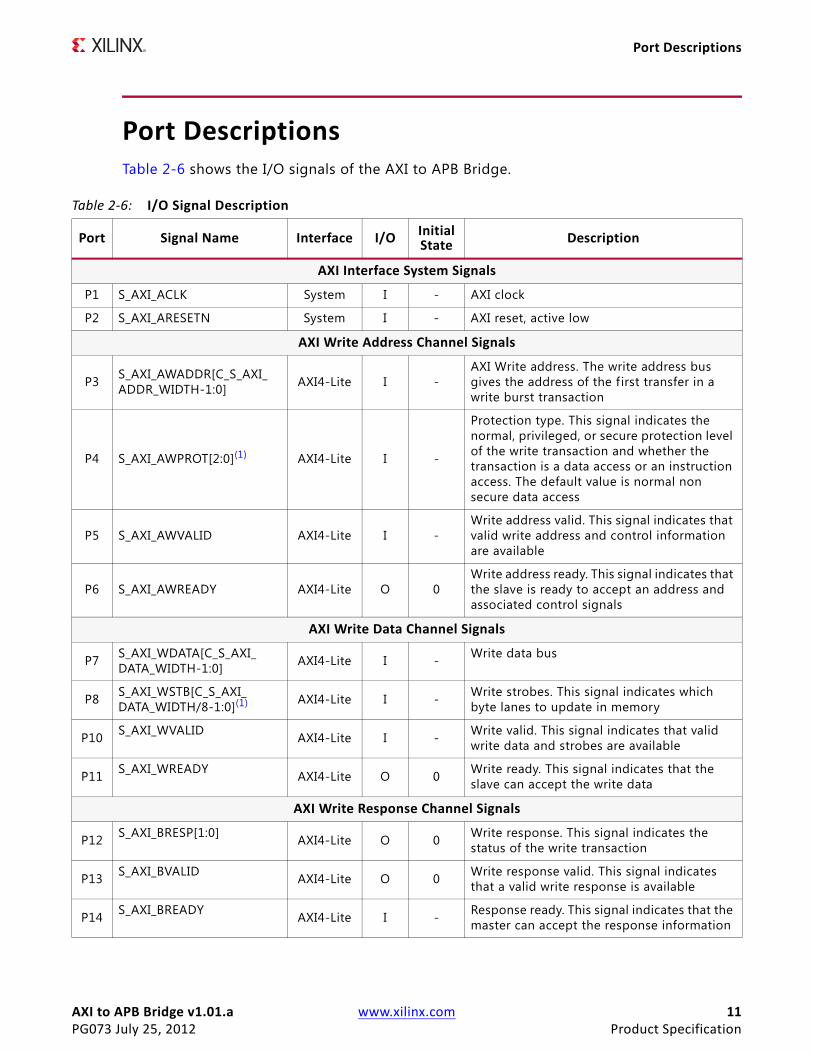
Customizing and Generating the CoreThis chapter includes information on using the Vivado™ Design Suite to customize and generate the core.
GUIThe AXI to APB Bridge can be found in AXI_Infrastructure\Interconnect in the Vivado Design Suite graphical user interface (GUI) View by Function pane.
To access the AXI to APB Bridge, do the following:
1. Open a project by selecting File > Open Project or create a new project by selecting File > New Project.
2. With an open project, choose AXI_Infrastructure in the View by Function pane.
3. Double-click AXI APB Bridge to bring up the AXI APB Bridge GUI.
AXI APB Bridge GUI contains two pages for configuration of the core. The f irst page contains the basic configurations like number of APB slaves, APB protocol, and time-out value. The second page contains the APB slave base addresses and high addresses. Each slave base address/ high address need to be configured in the Slave addresses page.
AXI to APB Bridge v1.01.a www.xilinx.com 23PG073 July 25, 2012
GUI
X-Ref Target - Figure 4-1
Figure 4-1: AXI APB GUI Screenshot

AXI to APB Bridge v1.01.a www.xilinx.com 24PG073 July 25, 2012
Appendix A
MigratingFor information on migrating to the Vivado™ Design Suite, see UG911, Vivado Design Suite Migration Methodology Guide [Ref 2].

AXI to APB Bridge v1.01.a www.xilinx.com 25PG073 July 25, 2012
Appendix B
DebuggingSee Solution Centers in Appendix C for information helpful to the debugging progress.

AXI to APB Bridge v1.01.a www.xilinx.com 26PG073 July 25, 2012
Appendix C
Additional Resources
Xilinx ResourcesFor support resources such as Answers, Documentation, Downloads, and Forums, see the Xilinx Support website at:
www.xilinx.com/support.
For a glossary of technical terms used in Xilinx documentation, see:
www.xilinx.com/company/terms.htm.
Solution CentersSee the Xilinx Solution Centers for support on devices, software tools, and intellectual property at all stages of the design cycle. Topics include design assistance, advisories, and troubleshooting tips.
ReferencesThese documents provide supplemental material useful with this product guide:
1. ARM® AMBA® documentation (infocenter.arm.com/help/index.jsp?topic=/com.arm.doc.ihi0051a/index.html):
° AMBA AXI and ACE Protocol Specification, AXI3, AXI4, and AXI4-Lite, v2.0
° AMBA APB Protocol Specification v2.0
2. Vivado Design Suite documentation: www.xilinx.com/cgi-bin/docs/rdoc?v=2012.2;t=vivado+userguides
3. Xilinx Device and IP documentation (www.xilinx.com/support):
° DS150, Virtex-6 Family Overview

AXI to APB Bridge v1.01.a www.xilinx.com 27PG073 July 25, 2012
Technical Support
° DS160, Spartan-6 Family Overview
° DS180, 7 Series FPGAs Overview
° DS768, LogiCORE IP AXI Interconnect Data Sheet
Technical SupportXilinx provides technical support at www.xilinx.com/support for this LogiCORE™ IP product when used as described in the product documentation. Xilinx cannot guarantee timing, functionality, or support of product if implemented in devices that are not defined in the documentation, if customized beyond that allowed in the product documentation, or if changes are made to any section of the design labeled DO NOT MODIFY.
See the Embedded Edition Derivative Device Support web page (www.xilinx.com/ise/embedded/ddsupport.htm) for a complete list of supported derivative devices for this core.
Revision HistoryThe following table shows the revision history for this document.
Notice of DisclaimerThe information disclosed to you hereunder (the “Materials”) is provided solely for the selection and use of Xilinx products. To the maximum extent permitted by applicable law: (1) Materials are made available “AS IS” and with all faults, Xilinx hereby DISCLAIMS ALL WARRANTIES AND CONDITIONS, EXPRESS, IMPLIED, OR STATUTORY, INCLUDING BUT NOT LIMITED TO WARRANTIES OF MERCHANTABILITY, NON-INFRINGEMENT, OR FITNESS FOR ANY PARTICULAR PURPOSE; and (2) Xilinx shall not be liable (whether in contract or tort, including negligence, or under any other theory of liability) for any loss or damage of any kind or nature related to, arising under, or in connection with, the Materials (including your use of the Materials), including for any direct, indirect, special, incidental, or consequential loss or damage (including loss of data, profits, goodwill, or any type of loss or damage suffered as a result of any action brought by a third party) even if such damage or loss was reasonably foreseeable or Xilinx had been advised of the possibility of the same. Xilinx assumes no obligation to correct any errors contained in the Materials or to notify you of updates to the Materials or to product specifications. You may not reproduce, modify, distribute, or publicly display the Materials without prior written consent. Certain products are subject to the terms and conditions of the Limited Warranties which can be viewed at http://www.xilinx.com/warranty.htm; IP cores may be subject to warranty and support terms contained in a license issued to you by Xilinx. Xilinx products are not designed or intended to be fail-safe or for use in any application requiring fail-safe performance; you assume sole risk and liability for use of Xilinx products in Critical Applications: http://www.xilinx.com/warranty.htm#critapps.© Copyright 2012 Xilinx, Inc. Xilinx, the Xilinx logo, Artix, ISE, Kintex, Spartan, Virtex, Vivado, Zynq, and other designated brands included herein are trademarks of Xilinx in the United States and other countries. All other trademarks are the property of their respective owners.
Date Version Revision
07/25/12 1.0 Initial Xilinx release. This release supports Vivado Design Suite 2012.2 and Xilinx Platform Studio. This document replaces DS788, LogiCORE IP AXI to APB Bridge Data Sheet.


![System Verilog/UVM Verification of AMBA APB Protocol · 2021. 6. 10. · bridge (simply APB bridge) acts as the Master and initiates all the transactions [8]. This paper presents](https://img.dokumen.tips/doc/110x75/614869582918e2056c22abed/system-veriloguvm-verification-of-amba-apb-protocol-2021-6-10-bridge-simply.jpg)


![LogiCORE IP AXI to APB Bridge v2 - XilinxThe 32-bit AXI4-Lite interface on the AXI to APB Bridge core is based on the AMBA AXI and ACE Protocol Specification v2.0 [Ref 1]. The core](https://img.dokumen.tips/doc/110x75/5ea76a1bf3eb741af75f6d89/logicore-ip-axi-to-apb-bridge-v2-xilinx-the-32-bit-axi4-lite-interface-on-the.jpg)