Embed Size (px)
Citation preview

LMH6611, LMH6612
www.ti.com SNOSB00K –NOVEMBER 2007–REVISED OCTOBER 2013
LMH6611/LMH6612 Single Supply 345 MHz Rail-to-Rail Output AmplifiersCheck for Samples: LMH6611, LMH6612
1FEATURES DESCRIPTIONThe LMH6611 (single, with shutdown) and LMH6612
23• VS = 5V, RL = 1 kΩ, TA = 25°C and AV = +1,(dual) are 345 MHz rail-to-rail output amplifiersUnless Otherwise Specified.consuming just 3.2 mA of quiescent current per
• Operating Voltage Range 2.7V to 11V channel and designed to deliver high performance in• Supply Current Per Channel 3.2 mA power conscious single supply systems. The
LMH6611 and LMH6612 have precision trimmed• Small Signal Bandwidth 345 MHzinput offset voltages with low noise and low distortion• Open Loop Gain 103 dB performance as required for high accuracy video, test
• Input Offset Voltage (Limit at 25°C) ±1.5 mV and measurement, and communication applications.The LMH6611 and LMH6612 are members of the• Slew Rate 460 V/µsPowerWise family and have an exceptional power-to-• 0.1 dB Bandwidth 45 MHz performance ratio.
• Settling Time to 0.1% 67 nsWith a trimmed input offset voltage of 0.022 mV and• Settling Time to 0.01% 100 ns a high open loop gain of 103 dB the LMH6611 and
• SFDR (f = 100 kHz, AV = 2, VOUT = 2 VPP) 102 LMH6612 meet the requirements of DC sensitive highdBc speed applications such as low pass filtering in
baseband I and Q radio channels. These• Low Voltage Noise 10 nV/√Hzspecifications combined with a 0.01% settling time of• Output current ±100 mA 100 ns, a low noise of 10 nV/√Hz and better than 102
• CMVR −0.2V to 3.8V dBc SFDR at 100 kHz make these amplifiersparticularly suited to driving 10, 12 and 14-bit high• Rail-to-Rail Outputspeed ADCs. The 45 MHz 0.1 dB bandwidth (AV = 2)• −40°C to +125°C Temperature Range driving 2 VPP into 150Ω allows the amplifiers to beused as output drivers in 1080i and 720p HDTVAPPLICATIONS applications.
• ADC Driver The input common mode range extends from 200 mV• DAC Buffer below the negative supply rail up to 1.2V from the
positive rail. On a single 5V supply with a ground• Active Filtersterminated 150Ω load the output swings to within 49• High Speed Sensor Amplifier mV of the ground, while a mid-rail terminated 1 kΩ
• Current Sense Amplifier load will swing to 77 mV of either rail.• 1080i and 720p Analog Video Amplifier• STB, TV Video Amplifier• Video Switching and Muxing
1
Please be aware that an important notice concerning availability, standard warranty, and use in critical applications ofTexas Instruments semiconductor products and disclaimers thereto appears at the end of this data sheet.
2WEBENCH is a registered trademark of Texas Instruments.3All other trademarks are the property of their respective owners.PRODUCTION DATA information is current as of publication date. Copyright © 2007–2013, Texas Instruments IncorporatedProducts conform to specifications per the terms of the TexasInstruments standard warranty. Production processing does notnecessarily include testing of all parameters.

LMH6611 ADC121S101
0.1 PF 10 PF0.1 PF 10 PF
0.1 PF
V+
0.01 PF R614.3 k:
0.1 PF1 PF
GND
5V
R5
1.24 k:
C2
1 nF
C5
150 pF
R2
549:
V+
-
+
RL
22:
CL
390 pF
R1
549:IN
1 PF
V+
R7
14.3 k:
5.6 PFU1
LMH6611, LMH6612
SNOSB00K –NOVEMBER 2007–REVISED OCTOBER 2013 www.ti.com
DESCRIPTION (CONTINUED)The amplifiers will operate on a 2.7V to 11V single supply or ±1.35V to ±5.5V split supply. The LMH6611 singleis available in 6-Pin SOT and has an independent active low disable pin which reduces the supply current to 120µA. The LMH6612 is available in 8-Pin SOIC. Both the LMH6611 and LMH6612 are available in −40°C to+125°C extended industrial temperature grade.
Typical Application
These devices have limited built-in ESD protection. The leads should be shorted together or the device placed in conductive foamduring storage or handling to prevent electrostatic damage to the MOS gates.
Absolute Maximum Ratings (1) (2)
For input pins only 2000VHuman Body Model
For all other pins 2000VESD Tolerance (3)
Machine Model 200VCharge Device Model 1000V
Supply Voltage (VS = V+ – V−) 12VJunction Temperature (4) 150°C max
(1) Absolute Maximum Ratings indicate limits beyond which damage to the device may occur. Operating Ratings indicate conditions forwhich the device is intended to be functional, but specific performance is not ensured. For ensured specifications and the testconditions, see the Electrical Characteristics.
(2) If Military/Aerospace specified devices are required, please contact the Texas Instruments Sales Office/ Distributors for availability andspecifications.
(3) Human Body Model, applicable std. MIL-STD-883, Method 3015.7. Machine Model, applicable std. JESD22-A115-A (ESD MM std. ofJEDEC)Field-Induced Charge-Device Model, applicable std. JESD22-C101-C (ESD FICDM std. of JEDEC).
(4) The maximum power dissipation is a function of TJ(MAX), θJA. The maximum allowable power dissipation at any ambient temperature isPD = (TJ(MAX)) – TA)/ θJA. All numbers apply for packages soldered directly onto a PC Board.
Operating Ratings (1)
Supply Voltage (VS = V+ – V−) 2.7V to 11VAmbient Temperature Range (2) −40°C to +125°C
6-Pin SOT 231°C/WPackage Thermal Resistance (θJA)
8-Pin SOIC 160°C/W
(1) Absolute Maximum Ratings indicate limits beyond which damage to the device may occur. Operating Ratings indicate conditions forwhich the device is intended to be functional, but specific performance is not ensured. For ensured specifications and the testconditions, see the Electrical Characteristics.
(2) The maximum power dissipation is a function of TJ(MAX), θJA. The maximum allowable power dissipation at any ambient temperature isPD = (TJ(MAX)) – TA)/ θJA. All numbers apply for packages soldered directly onto a PC Board.
2 Submit Documentation Feedback Copyright © 2007–2013, Texas Instruments Incorporated
Product Folder Links: LMH6611 LMH6612

LMH6611, LMH6612
www.ti.com SNOSB00K –NOVEMBER 2007–REVISED OCTOBER 2013
+3V Electrical CharacteristicsUnless otherwise specified, all limits are specified for TJ = +25°C, V+ = 3V, V− = 0V, VS = V+ – V−, DISABLE = 3V, VCM = VO =V+/2, AV = +1, RF = 0Ω, when AV ≠ +1 then RF = 560Ω, RL = 1 kΩ. Boldface limits apply at temperature extremes. (1)
Symbol Parameter Condition Min (2) Typ (3) Max (2) UnitsFrequency Domain ResponseSSBW –3 dB Bandwidth Small Signal AV = 1, RL = 1 kΩ, VOUT = 0.2 VPP 305
MHzAV = 2, −1, RL = 1 kΩ, VOUT = 0.2 VPP 115
GBW Gain Bandwidth AV = 10, RF = 2 kΩ, RG = 221Ω, RL = 1 kΩ, 115 135(LMH6611) VOUT = 0.2 VPP MHzGain Bandwidth AV = 10, RF = 2 kΩ, RG = 221Ω, RL = 1 kΩ, 130(LMH6612) VOUT = 0.2 VPP
LSBW −3 dB Bandwidth Large Signal AV = 1, RL = 1 kΩ, VOUT = 1.5 VPP 90MHz
AV = −1, RL = 150Ω, VOUT = 2 VPP 85Peak Peaking AV = 1 1.0 dB0.1 0.1 dB Bandwidth AV = 1, VOUT = 0.5 VPP, RL = 1 kΩ 33dBBW AV = 2, VOUT = 0.5 VPP, RL = 1 kΩ 65
RF = RG = 560Ω MHzAV = 2, VOUT = 1.5 VPP, RL = 150Ω, 47RF = RG = 510Ω
DG Differential Gain AV = 2, 4.43 MHz, 0.6V < VOUT < 2V, 0.03 %RL = 150Ω to V+/2
DP Differential Phase AV = 2, 4.43 MHz, 0.6V < VOUT < 2V, 0.06 degRL = 150Ω to V+/2
Time Domain Responsetr/tf Rise & Fall Time 1.5V Step, AV = 1 2.8 nsSR Slew Rate 2V Step, AV = 1 330 V/μsts_0.1 0.1% Settling Time 2V Step, AV = −1 74
nsts_0.01 0.01% Settling Time 2V Step, AV = −1 116Noise and Distortion PerformanceSFDR Spurious Free Dynamic Range fC = 100 kHz, AV = −1, VOUT= 2 VPP 109
fC = 1 MHz, AV = −1, VOUT = 2 VPP 97 dBcfC = 5 MHz, AV = −1, VOUT = 2 VPP 80
en Input Voltage Noise f = 100 kHz 10 nV/√Hzin Input Current Noise f = 100 kHz 2 pA/√HzCT Crosstalk (LMH6612) f = 5 MHz, VIN = 2 VPP 71 dBInput, DC PerformanceVOS Input Offset Voltage (LMH6611) VCM = 0.5V 0.022 ±1.5
±2mV
Input Offset Voltage (LMH6612) VCM = 0.5V −0.015 ±1.5±2
TCVOS Input Offset Voltage Average Drift See (4) 4 μV/°CIB Input Bias Current VCM = 0.5V −5.9 −10.1 μA−11.1IO Input Offset Current 0.01 ±0.5 μA±0.7CIN Input Capacitance 2.5 pFRIN Input Resistance 6 MΩCMVR Input Voltage Range DC, CMRR ≥ 76 dB −0.2 1.8 V
(1) Boldface limits apply to temperature range of −40°C to 125°C(2) Limits are 100% production tested at 25°C. Limits over the operating temperature range are ensured through correlations using the
Statistical Quality Control (SQC) method.(3) Typical values represent the most likely parametric norm as determined at the time of characterization. Actual typical values may vary
over time and will also depend on the application and configuration. The typical values are not tested and are not ensured on shippedproduction material.
(4) Voltage average drift is determined by dividing the change in VOS by temperature change.
Copyright © 2007–2013, Texas Instruments Incorporated Submit Documentation Feedback 3
Product Folder Links: LMH6611 LMH6612

LMH6611, LMH6612
SNOSB00K –NOVEMBER 2007–REVISED OCTOBER 2013 www.ti.com
+3V Electrical Characteristics (continued)Unless otherwise specified, all limits are specified for TJ = +25°C, V+ = 3V, V− = 0V, VS = V+ – V−, DISABLE = 3V, VCM = VO =V+/2, AV = +1, RF = 0Ω, when AV ≠ +1 then RF = 560Ω, RL = 1 kΩ. Boldface limits apply at temperature extremes.(1)
Symbol Parameter Condition Min (2) Typ (3) Max (2) UnitsCMRR Common Mode Rejection Ratio VCM Stepped from −0.1V to 1.7V 79 98 dBAOL Open Loop Gain RL = 1 kΩ, VOUT = 2.7V to 0.3V 89 101
dBRL = 150Ω, VOUT = 2.5V to 0.5V 78 85
Output DC CharacteristicsVO Output Swing High (LMH6611) RL = 1 kΩ to V+/2 59 72
(Voltage from V+ Supply Rail) 76RL = 150Ω to V+/2 133 169
182Output Swing Low (LMH6611) RL = 1 kΩ to V+/2 59 74(Voltage from V− Supply Rail) 80
RL = 150Ω to V+/2 133 171188
RL = 150Ω to V− 42 5256
mVOutput Swing High (LMH6612) RL = 1 kΩ to V+/2 58 68(Voltage from V+ Supply Rail) 73
RL = 150Ω to V+/2 131 157172
Output Swing Low (LMH6612) RL = 1 kΩ to V+/2 61 71(Voltage from V− Supply Rail) 79
RL = 150Ω to V+/2 139 168187
RL = 150Ω to V− 43 5156
IOUT Linear Output Current VOUT = V+/2 (5) ±70 mARO Output Resistance f = 1 MHz 0.07 ΩEnable Pin Operation
Enable High Voltage Threshold Enabled (6) 2.0 VEnable Pin High Current VDISABLE = 3V 0.001 µAEnable Low Voltage Threshold Disabled (6) 1.0 VEnable Pin Low Current VDISABLE = 0V 0.8 µA
ton Turn-On Time 18 nstoff Turn-Off Time 50 nsPower Supply PerformancePSRR Power Supply Rejection Ratio DC, VCM = 0.5V, VS = 2.7V to 11V 81 96 dBIS Supply Current (LMH6611) RL = ∞ 3.0 3.4
3.8mA
Supply Current (LMH6612) RL = ∞ 2.95 3.45(per channel) 3.9
ISD Disable Shutdown Current DISABLE = 0V 101 132 μA(LMH6611)
(5) Do not short circuit the output. Continuous source or sink currents larger than the IOUT typical are not recommended as they maydamage the part.
(6) This parameter is ensured by design and/or characterization and is not tested in production.
4 Submit Documentation Feedback Copyright © 2007–2013, Texas Instruments Incorporated
Product Folder Links: LMH6611 LMH6612

LMH6611, LMH6612
www.ti.com SNOSB00K –NOVEMBER 2007–REVISED OCTOBER 2013
+5V Electrical CharacteristicsUnless otherwise specified, all limits are specified for TJ = +25°C, V+ = 5V, V− = 0V, VS = V+ – V−, DISABLE = 5V, VCM = VO =V+/2, AV = +1, RF = 0Ω, when AV ≠ +1 then RF = 560Ω, RL = 1 kΩ. Boldface limits apply at temperature extremes.
Symbol Parameter Condition Min Typ Max Units(1) (2) (1)
Frequency Domain ResponseSSBW –3 dB Bandwidth Small Signal AV = 1, RL = 1 kΩ, VOUT = 0.2 VPP 345
MHzAV = 2, −1, RL = 1 kΩ, VOUT = 0.2 VPP 112
GBW Gain Bandwidth (LMH6611) AV = 10, RF = 2 kΩ, RG = 221Ω, RL = 1 kΩ, 115 135VOUT = 0.2 VPP MHz
Gain Bandwidth (LMH6612) AV = 10, RF = 2 kΩ, RG = 221Ω, RL = 1 kΩ, 130VOUT = 0.2 VPP
LSBW −3 dB Bandwidth Large Signal AV = 1, RL = 1 kΩ, VOUT = 2 VPP 77MHz
AV = 2, RL = 150Ω, VOUT = 2 VPP 85Peak Peaking AV = 1 0.3 dB0.1 0.1 dB Bandwidth AV = 1, VOUT = 0.5 VPP, RL = 1 kΩ 45dBBW AV = 2, VOUT = 0.5 VPP, RL = 1 kΩ 68
RF = RG = 680Ω MHzAV = 2, VOUT = 2 VPP, RL = 150Ω, 45RF = RG = 665Ω
DG Differential Gain AV = 2, 4.43 MHz, 0.6V < VOUT < 2V, 0.05 %RL = 150Ω to V+/2
DP Differential Phase AV = 2, 4.43 MHz, 0.6V < VOUT < 2V, 0.06 degRL = 150Ω to V+/2
Time Domain Responsetr/tf Rise & Fall Time 2V Step, AV = 1 3.6 nsSR Slew Rate 2V Step, AV = 1 460 V/μsts_0.1 0.1% Settling Time 2V Step, AV = −1 67
nsts_0.01 0.01% Settling Time 2V Step, AV = −1 100Distortion and Noise PerformanceSFDR Spurious Free Dynamic Range fC = 100 kHz, AV = 2, VOUT = 2 VPP 102
fC = 1 MHz, AV = 2, VOUT = 2 VPP 96 dBcfC = 5 MHz, AV = 2, VO = 2 VPP 82
en Input Voltage Noise f = 100 kHz 10 nV/√Hzin Input Current Noise f = 100 kHz 2 pA/√HzCT Crosstalk (LMH6612) f = 5 MHz, VIN = 2 VPP 71 dBInput, DC PerformanceVOS Input Offset Voltage (LMH6611) VCM = 0.5V 0.013 ±1.5
±2mV
Input Offset Voltage (LMH6612) VCM = 0.5V 0.022 ±1.5±2
TCVOS Input Offset Voltage Average Drift See (3) 4 µV/°CIB Input Bias Current VCM = 0.5V −6.3 −10.1 μA−11.1IO Input Offset Current 0.01 ±0.5 μA±0.7CIN Input Capacitance 2.5 pFRIN Input Resistance 6 MΩCMVR Input Voltage Range DC, CMRR ≥ 78 dB −0.2 3.8 V
(1) Limits are 100% production tested at 25°C. Limits over the operating temperature range are ensured through correlations using theStatistical Quality Control (SQC) method.
(2) Typical values represent the most likely parametric norm as determined at the time of characterization. Actual typical values may varyover time and will also depend on the application and configuration. The typical values are not tested and are not ensured on shippedproduction material.
(3) Voltage average drift is determined by dividing the change in VOS by temperature change.
Copyright © 2007–2013, Texas Instruments Incorporated Submit Documentation Feedback 5
Product Folder Links: LMH6611 LMH6612

LMH6611, LMH6612
SNOSB00K –NOVEMBER 2007–REVISED OCTOBER 2013 www.ti.com
+5V Electrical Characteristics (continued)Unless otherwise specified, all limits are specified for TJ = +25°C, V+ = 5V, V− = 0V, VS = V+ – V−, DISABLE = 5V, VCM = VO =V+/2, AV = +1, RF = 0Ω, when AV ≠ +1 then RF = 560Ω, RL = 1 kΩ. Boldface limits apply at temperature extremes.
Symbol Parameter Condition Min Typ Max Units(1) (2) (1)
CMRR Common Mode Rejection Ratio VCM Stepped from −0.1V to 3.7V 81 98 dBAOL Open Loop Gain RL = 1 kΩ, VOUT = 4.6V to 0.4V 92 103
dBRL = 150Ω, VOUT = 4.4V to 0.6V 80 86
Output DC CharacteristicsVO Output Swing High (LMH6611) RL = 1 kΩ to V+/2 76 90
(Voltage from V+ Supply Rail) 93RL =150Ω to V+/2 195 239
256Output Swing Low (LMH6611) RL = 1 kΩ to V+/2 74 92(Voltage from V− Supply Rail) 98
RL =150Ω to V+/2 193 243265
RL = 150Ω to V− 48 6064
mVOutput Swing High (LMH6612) RL = 1 kΩ to V+/2 75 86(Voltage from V+ Supply Rail) 91
RL =150Ω to V+/2 195 223241
Output Swing Low (LMH6612) RL = 1 kΩ to V+/2 77 88(Voltage from V− Supply Rail) 98
RL =150Ω to V+/2 202 234261
RL = 150Ω to V− 49 5864
IOUT Linear Output Current VOUT = V+/2 (4) ±100 mARO Output Resistance f = 1 MHz 0.07 ΩEnable Pin Operation
Enable High Voltage Threshold Enabled (5) 3.0 VEnable Pin High Current VDISABLE = 5V 1.2 µAEnable Low Voltage Threshold Disabled (5) 2.0 VEnable Pin Low Current VDISABLE = 0V 2.8 µA
ton Turn-On Time 20 nstoff Turn-Off Time 60 nsPower Supply PerformancePSRR Power Supply Rejection Ratio DC, VCM = 0.5V, VS = 2.7V to 11V 81 96 dBIS Supply Current (LMH6611) RL = ∞ 3.2 3.6
4.0mA
Supply Current (LMH6612) RL = ∞ 3.2 3.7(per channel) 4.25
ISD Disable Shutdown Current DISABLE = 0V 120 162 μA(LMH6611)
(4) Do not short circuit the output. Continuous source or sink currents larger than the IOUT typical are not recommended as they maydamage the part.
(5) This parameter is ensured by design and/or characterization and is not tested in production.
6 Submit Documentation Feedback Copyright © 2007–2013, Texas Instruments Incorporated
Product Folder Links: LMH6611 LMH6612

LMH6611, LMH6612
www.ti.com SNOSB00K –NOVEMBER 2007–REVISED OCTOBER 2013
±5V Electrical CharacteristicsUnless otherwise specified, all limits are specified for TJ = +25°C, V+ = 5V, V− = −5V, VS = V+ – V−, DISABLE = 5V, VCM = VO= 0V, AV = +1, RF = 0Ω, when AV ≠ +1 then RF = 560Ω, RL = 1 kΩ. Boldface limits apply at temperature extremes.
Symbol Parameter Condition Min Typ Max Units(1) (2) (1)
Frequency Domain ResponseSSBW –3 dB Bandwidth Small Signal AV = 1, RL = 1 kΩ, VOUT = 0.2 VPP 365
MHzAV = 2, −1, RL = 1 kΩ, VOUT = 0.2 VPP 110
GBW Gain Bandwidth (LMH6611) AV = 10, RF = 2 kΩ, RG = 221Ω, RL = 1 kΩ, 115 135VOUT = 0.2 VPP MHz
Gain Bandwidth (LMH6612) AV = 10, RF = 2 kΩ, RG = 221Ω, RL = 1 kΩ, 130VOUT = 0.2 VPP
LSBW −3 dB Bandwidth Large Signal AV = 1, RL = 1 kΩ, VOUT = 2 VPP 85MHz
AV = 2, RL = 150Ω, VOUT = 2 VPP 87Peak Peaking AV = 1 0.01 dB0.1 0.1 dB Bandwidth AV = 1, VOUT = 0.5 VPP, RL = 1 kΩ 92dBBW AV = 2, VOUT = 0.5 VPP, RL = 1 kΩ 65
RF = RG = 750Ω MHzAV = 2, VOUT = 2 VPP, RL = 150Ω, 45RF = RG = 680Ω
DG Differential Gain AV = 2, 4.43 MHz, 0.6V < VOUT < 2V, 0.05 %RL = 150Ω to V+/2
DP Differential Phase AV = 2, 4.43 MHz, 0.6V < VOUT < 2V, 0.05 degRL = 150Ω to V+/2
Time Domain Responsetr/tf Rise & Fall Time 2V Step, AV = 1 3.5 nsSR Slew Rate 2V Step, AV = 1 460 V/μsts_0.1 0.1% Settling Time 2V Step, AV = −1 60
nsts_0.01 0.01% Settling Time 2V Step, AV = −1 100Noise and Distortion PerformanceSFDR Spurious Free Dynamic Range fC = 100 kHz, AV = 2, VOUT = 2 VPP 102
fC = 1 MHz, AV = 2, VOUT = 2 VPP 100 dBcfC = 5 MHz, AV = 2, VOUT = 2 VPP 81
en Input Voltage Noise f = 100 kHz 10 nV/√Hzin Input Current Noise f = 100 kHz 2 pA/√HzCT Crosstalk (LMH6612) f = 5 MHz, VIN = 2 VPP 71 dBInput DC PerformanceVOS Input Offset Voltage (LMH6611) VCM = −4.5V 0.074 ±1.5
±2mV
Input Offset Voltage (LMH6612) VCM = −4.5V 0.095 ±1.5±2
TCVOS Input Offset Voltage Average Drift See (3) 4 µV/°CIB Input Bias Current VCM = −4.5V −6.5 −10.1 μA−11.1IO Input Offset Current 0.01 ±0.5 μA±0.7CIN Input Capacitance 2.5 pFRIN Input Resistance 6 MΩCMVR Input Voltage Range DC, CMRR ≥ 81 dB −5.2 3.8 V
(1) Limits are 100% production tested at 25°C. Limits over the operating temperature range are ensured through correlations using theStatistical Quality Control (SQC) method.
(2) Typical values represent the most likely parametric norm as determined at the time of characterization. Actual typical values may varyover time and will also depend on the application and configuration. The typical values are not tested and are not ensured on shippedproduction material.
(3) Voltage average drift is determined by dividing the change in VOS by temperature change.
Copyright © 2007–2013, Texas Instruments Incorporated Submit Documentation Feedback 7
Product Folder Links: LMH6611 LMH6612

LMH6611, LMH6612
SNOSB00K –NOVEMBER 2007–REVISED OCTOBER 2013 www.ti.com
±5V Electrical Characteristics (continued)Unless otherwise specified, all limits are specified for TJ = +25°C, V+ = 5V, V− = −5V, VS = V+ – V−, DISABLE = 5V, VCM = VO= 0V, AV = +1, RF = 0Ω, when AV ≠ +1 then RF = 560Ω, RL = 1 kΩ. Boldface limits apply at temperature extremes.
Symbol Parameter Condition Min Typ Max Units(1) (2) (1)
CMRR Common Mode Rejection Ratio VCM Stepped from −5.1V to 3.7V 81 98 dBAOL Open Loop Gain RL = 1 kΩ, VOUT = +4.6V to −4.6V 96 103
dBRL = 150Ω, VOUT = +4.3V to −4.3V 80 87
Output DC CharacteristicsVO Output Swing High (LMH6611) RL = 1 kΩ to GND 107 125
(Voltage from V+ Supply Rail) 130RL = 150Ω to GND 339 402
433Output Swing Low (LMH6611) RL = 1 kΩ to GND 103 123(Voltage from V− Supply Rail) 132
RL = 150Ω to GND 332 404445
RL = 150Ω to V− 54 7074
mVOutput Swing High (LMH6612) RL = 1 kΩ to GND 107 118(Voltage from V+ Supply Rail) 125
RL = 150Ω to GND 340 375407
Output Swing Low (LMH6612) RL = 1 kΩ to GND 108 120(Voltage from V− Supply Rail) 135
RL = 150Ω to GND 348 389434
RL = 150Ω to V− 56 6674
IOUT Linear Output Current VOUT = GND (4) ±120 mARO Output Resistance f = 1 MHz 0.07 ΩEnable Pin Operation
Enable High Voltage Threshold Enabled (5) 0.5 VEnable Pin High Current VDISABLE = +5V 17.0 µAEnable Low Voltage Threshold Disabled (5) −0.5 VEnable Pin Low Current VDISABLE = −5V 18.6 µA
ton Turn-On Time 19 nstoff Turn-Off Time 60 nsPower Supply PerformancePSRR Power Supply Rejection Ratio DC, VCM = −4.5V, VS = 2.7V to 11V 81 96 dBIS Supply Current (LMH6611) RL = ∞ 3.3 3.8
4.4mA
Supply Current (LMH6612) RL = ∞ 3.45 4.05(per channel) 4.85
ISD Disable Shutdown Current DISABLE = −5V 160 212 μA(LMH6611)
(4) Do not short circuit the output. Continuous source or sink currents larger than the IOUT typical are not recommended as they maydamage the part.
(5) This parameter is ensured by design and/or characterization and is not tested in production.
8 Submit Documentation Feedback Copyright © 2007–2013, Texas Instruments Incorporated
Product Folder Links: LMH6611 LMH6612

OUT B
1
2
3
4 5
6
7
8OUT A
-IN A
+IN A
V-
V+
-IN B
+IN B
- +
+ -
A
B
VOUT
V-
+IN
V+
-IN
+ -
1
2
3
6
4
5DISABLE
LMH6611, LMH6612
www.ti.com SNOSB00K –NOVEMBER 2007–REVISED OCTOBER 2013
Connection Diagram
Figure 1. 6-Pin SOT Figure 2. 8-Pin SOICTop View Top View
Copyright © 2007–2013, Texas Instruments Incorporated Submit Documentation Feedback 9
Product Folder Links: LMH6611 LMH6612

1 10 100 1000
FREQUENCY (MHz)
-18
-15
-12
-9
-6
-3
0
3
6
GA
IN (
dB)
V+ = +2.5V
V- = -2.5V
VOUT = 0.2V
RL = 150:
CL = 6 pFA = +1
125°C25°C
-40°C
1 10 100 1000
FREQUENCY (MHz)
-18
-15
-12
-9
-6
-3
0
3
6
9
GA
IN (
dB)
V+ = +2.5V
V- = -2.5V
VOUT = 0.2V
RL = 1 k:
CL = 6 pFA = +1
125°C
25°C
-40°C
1 10 100 1000
FREQUENCY (MHz)
-21
-18
-15
-12
-9
-6
-3
0
3
NO
RM
ALI
ZE
D G
AIN
(dB
)
A = +2
VOUT = 0.2V
RL = 150:
RF = 560:
3V 5V
10V
1 10 100 1000
FREQUENCY (MHz)
-15
-12
-9
-6
-3
0
3
GA
IN (
dB)
A = +1
VOUT = 0.2V
RL = 150:
3V5V
10V
1 10 100 1000
FREQUENCY (MHz)
-21
-18
-15
-12
-9
-6
-3
0
3
GA
IN (
dB)
A = +1
VOUT = 0.2V
RL = 1 k:
±1.5V
±2.5V
±5V
1 10 100 1000
FREQUENCY (MHz)
-18
-15
-12
-9
-6
-3
0
3
NO
RM
ALI
ZE
D G
AIN
(dB
)
A = +2
VOUT = 0.2V
RL = 1 k:
±1.5V
±5V±2.5V
LMH6611, LMH6612
SNOSB00K –NOVEMBER 2007–REVISED OCTOBER 2013 www.ti.com
Typical Performance CharacteristicsAt TJ = 25°C, AV = +1 (RF = 0Ω), otherwise RF = 560Ω for AV ≠ +1, unless otherwise specified.
Closed Loop Frequency Response for Closed Loop Frequency Response forVarious Supplies Various Supplies
Figure 3. Figure 4.
Closed Loop Frequency Response for Closed Loop Frequency Response forVarious Supplies Various Supplies (Gain = +2)
Figure 5. Figure 6.
Closed Loop GainClosed Loop Gain vs.
vs. Frequency forFrequency for Various Temperatures Various Temperatures
Figure 7. Figure 8.
10 Submit Documentation Feedback Copyright © 2007–2013, Texas Instruments Incorporated
Product Folder Links: LMH6611 LMH6612

1 10 100-1.0-0.9-0.8-0.7-0.6-0.5-0.4-0.3-0.2-0.10.00.10.20.30.40.50.60.70.80.91.0
NO
RM
ALI
ZE
D G
AIN
(dB
FREQUENCY (MHz)
±5V, RF = RG = 750:
±2.5V, RF = RG = 680:
±1.5V, RF = RG = 560:
A = +2
VOUT = 0.5V
RL = 1 k:
1 10 100-1.0
-0.8
0.0
0.3
GA
IN (
dB)
0.2
0.1
-0.6-0.7
-0.9
-0.4
-0.3
-0.2
-0.1
FREQUENCY (MHz)
-0.5
A = -1
VOUT = 2V
RL = 150:
10V, RF = 750:
5V, RF = 604:
3V, RF = 560:
1 10 100 1000
FREQUENCY (MHz)
-18
-15
-12
-9
-6
-3
0
3
NO
RM
ALI
ZE
D G
AIN
(dB
)
±2.5V, = A = +2
±5V, A = +2
±1.5V, A = -1
VOUT = 2V
RL = 150:
1 10 100 1000-1.0-0.9-0.8-0.7-0.6-0.5-0.4-0.3-0.2-0.10.00.10.20.30.40.50.60.70.80.91.0
GA
IN (
dB
FREQUENCY (MHz)
A = +1
VOUT = 0.5V
RL = 1 k:
±1.5V±2.5V
±5V
1 10 100 1000
FREQUENCY (MHz)
-18
-15
-12
-9
-6
-3
0
3
GA
IN (
dB)
±1.5V, VOUT = 1.5V
A = +1
RL = 1 k:
±2.5V, VOUT = 2V
±5V, VOUT = 2V
1 10 100 1000
FREQUENCY (MHz)
-18
-15
-12
-9
-6
-3
0
3
NO
RM
ALI
ZE
D G
AIN
(dB
)
V+ = +2.5V
V- = -2.5V
RL = 1 k:
VOUT = 0.2V
A = 1
A = 2
A = 5
A = 10
LMH6611, LMH6612
www.ti.com SNOSB00K –NOVEMBER 2007–REVISED OCTOBER 2013
Typical Performance Characteristics (continued)At TJ = 25°C, AV = +1 (RF = 0Ω), otherwise RF = 560Ω for AV ≠ +1, unless otherwise specified.
Closed Loop Gainvs.
Frequency forVarious Gains Large Signal Frequency Response
Figure 9. Figure 10.
Large Signal Frequency Response ±0.1 dB Gain Flatness for Various Supplies
Figure 11. Figure 12.
±0.1 dB Gain Flatness for Various Supplies ±0.1 dB Gain Flatness for Various Supplies
Figure 13. Figure 14.
Copyright © 2007–2013, Texas Instruments Incorporated Submit Documentation Feedback 11
Product Folder Links: LMH6611 LMH6612

0.1 50
FREQUENCY (MHz)
-120
-80
-40
0
DIS
TO
RT
ION
(dB
c)
101
-20
-60
-100
-110
-90
-70
-50
-30
-10VOUT = 2 VPP
RL = 1 k:A = +1
HD2
V+ = +2.5V
V- = -2.5V
HD3
V+ = +2.5V
V- = -2.5V
HD3
V+ = +5V
V- = -5V
HD2
V+ = +5V
V- = -5V
0.1 50
FREQUENCY (MHz)
-120
-80
-40
0
DIS
TO
RT
ION
(dB
c)
101
-20
-60
-100
-110
-90
-70
-50
-30
-10
HD2
HD3 RL = 1 k:
RL = 150:
V+ = +2.5V
V- = -2.5V
VOUT = 2 VPPA = +1
-12
-9
-6
-3
0
3
6
9
GA
IN (
dB)
1 10 100 1000
FREQUENCY (MHz)
V+ = +2.5V
V- = -2.5V
A = +1
VOUT = 0.2V
RL = 1 k:
CL = 10 pF
CL = 7 pF
CL = 5.5 pF
CL = 3.3 pF
CL = 2 pF
-21
-18
-15
-12
-9
-6
-3
0
3
6
9
GA
IN (
dB)
1 10 100 1000
FREQUENCY (MHz)
V+ = +2.5V
V- = -2.5V
AV = +1
VOUT = 0.1V
CL = 100 pF
RL = 1 k:
RISO = 10
RISO = 20
RISO = 25
RISO = 30
1 10 100 1000
FREQUENCY MHz
-1.0
-0.8
0
0.3
NO
RM
ALI
ZE
D G
AIN
(dB
)
0.2
0.1
-0.6-0.7
-0.9
-0.4
-0.3
-0.2
-0.1
-0.5
3V, RF = 510:,
VOUT = 1.5V
10V, RF = 680:,
VOUT = 2V5V, RF = 665:,
VOUT = 2V
A = +2
RL = 150:
1 10 100 1000-1
-0.8
0
0.30.2
0.1
-0.6-0.7
-0.9
-0.4
-0.3
-0.2
-0.1
-0.5
A = +1
VOUT = 2V
RL = 150:
5V
10V
3V
FREQUENCY (MHz)
GA
IN (
dB)
LMH6611, LMH6612
SNOSB00K –NOVEMBER 2007–REVISED OCTOBER 2013 www.ti.com
Typical Performance Characteristics (continued)At TJ = 25°C, AV = +1 (RF = 0Ω), otherwise RF = 560Ω for AV ≠ +1, unless otherwise specified.
±0.1 dB Gain Flatness for Various Supplies ±0.1 dB Gain Flatness for Various Supplies (Gain = +2)
Figure 15. Figure 16.
Small Signal Frequency Response with Small Signal Frequency Response withVarious Capacitive Load Capacitive Load and Various RISO
Figure 17. Figure 18.
HD2 and HD3 HD2 and HD3vs. vs.
Frequency and Supply Voltage Frequency and Load
Figure 19. Figure 20.
12 Submit Documentation Feedback Copyright © 2007–2013, Texas Instruments Incorporated
Product Folder Links: LMH6611 LMH6612

120
1k 100k 10M 1G
FREQUENCY (Hz)
-40
0
60
GA
IN (
dB)
100M1M10k
100
80
40
20
-20
GAIN
PHASE
V+ = +2.5V
V- = -2.5V
RL = 1 k:
120
-120
-60
30
90
60
0
-30
-90
PH
AS
E (
°)
0 1 2 3 4 5-120
-110
-100
-90
-80
-70
-60
-50
-40
-30
-20
DIS
TO
RT
ION
(dB
c)
VOUT (VPP)
-10V
+ = +2.5V
V- = -2.5V
A = -1
RL = 1 k:
50 MHz
20 MHz
10 MHz
5 MHz
2 MHz
1 MHz
0.1 50
FREQUENCY (MHz)
-120
-80
-40
0
DIS
TO
RT
ION
(dB
c)
101
-20
-60
-100
-110
-90
-70
-50
-30
-10 V+ = +2.5V
V- = -2.5V
VOUT = 2 VPP
RL = 1 k:
RF = 560:
G = +1, HD2
G = +2, HD2
G = +10, HD2
0.1 50
FREQUENCY (MHz)
-120
-80
-40
0
DIS
TO
RT
ION
(dB
c)
101
-20
-60
-100
-110
-90
-70
-50
-30
-10 V+ = +2.5V
V- = -2.5V
VOUT = 2 VPP
RL = 1 k:
RF = 560:
G = +1, HD3
G = +2, HD3
G = +10, HD3
0 1 2 3 4 5 6 7 8 9 10-110
-100
-90
-80
-70
-60
-50
DIS
TO
RT
ION
(dB
c)
INPUT COMMON MODE VOLTAGE
HD2
V+ = +2.5V
V- = -2.5V
HD3
V+ = +2.5V
V- = -2.5V
HD3
V+ = +5V
V- = -5V
HD2
V+ = +5V
V- = -5V
f = 1 MHz
0 1 2 3 4 5 6 7 8 9 10-110
-100
-90
-80
-70
-60
-50
DIS
TO
RT
ION
(dB
c)
INPUT COMMON MODE VOLTAGE
HD2
V+ = +2.5V
V- = -2.5V
HD3
V+ = +2.5V
V- = -2.5V
HD3
V+ = +5V
V- = -5V
HD2
V+ = +5V
V- = -5V
f = 5 MHz
LMH6611, LMH6612
www.ti.com SNOSB00K –NOVEMBER 2007–REVISED OCTOBER 2013
Typical Performance Characteristics (continued)At TJ = 25°C, AV = +1 (RF = 0Ω), otherwise RF = 560Ω for AV ≠ +1, unless otherwise specified.
HD2 and HD3 HD2 and HD3vs. vs.
Common Mode Voltage Common Mode Voltage
Figure 21. Figure 22.
HD2 HD3vs. vs.
Frequency and Gain Frequency and Gain
Figure 23. Figure 24.
HD2vs.
Open Loop Gain and Phase Output Swing
Figure 25. Figure 26.
Copyright © 2007–2013, Texas Instruments Incorporated Submit Documentation Feedback 13
Product Folder Links: LMH6611 LMH6612
0 0.5 1 1.5 2 2.5 3 3.5 4 4.50
10
20
30
40
50
60
70
80
90
SE
TT
LIN
G T
IME
(ns
)
OUTPUT SWING (VPP)
V+ = +2.5V
V- = -2.5V
AV = -1
RISING, 0.1%
FALLING, 0.1%
0 1 2 3 4 5-120
-110
-100
-90
-80
-70
-60
-50
-40
-30
-20
DIS
TO
RT
ION
(dB
c)
VOUT (VPP)
-10
0
50 MHz
20 MHz
10 MHz5 MHz
2 MHz
1 MHz
V+ = +2.5V
V- = -2.5V
A = +2
RL = 150:
0 1 2 3 4 5-120
-110
-100
-90
-80
-70
-60
-50
-40
-30
-20
DIS
TO
RT
ION
(dB
c)
VOUT (VPP)
-10V
+ = +2.5V
V- = -2.5V
A = +2
RL = 150:
50 MHz
20 MHz
10 MHz 5 MHz
2 MHz
1 MHz
0 1 2 3 4 5-120
-110
-100
-90
-80
-70
-60
-50
-40
-30
-20
DIS
TO
RT
ION
(dB
c)
VOUT (VPP)
-10V
+ = +2.5V
V- = -2.5V
A = +2
RL = 1 k:
50 MHz
20 MHz
10 MHz
5 MHz
2 MHz
1 MHz
0 1 2 3 4 5-110
-100
-90
-80
-70
-60
-50
-40
-30
-20
DIS
TO
RT
ION
(dB
c)
VOUT (VPP)
-10V
+ = +2.5V
V- = -2.5V
A = -1
RL = 1 k:
50 MHz
20 MHz
10 MHz
5 MHz
2 MHz
1 MHz
0 1 2 3 4 5-120
-110
-100
-90
-80
-70
-60
-50
-40
-30
-20
DIS
TO
RT
ION
(dB
c)
VOUT (VPP)
-10V
+ = +2.5V
V- = -2.5V
A = +2
RL = 1 k:
50 MHz
20 MHz
10 MHz
5 MHz2 MHz
1 MHz
LMH6611, LMH6612
SNOSB00K –NOVEMBER 2007–REVISED OCTOBER 2013 www.ti.com
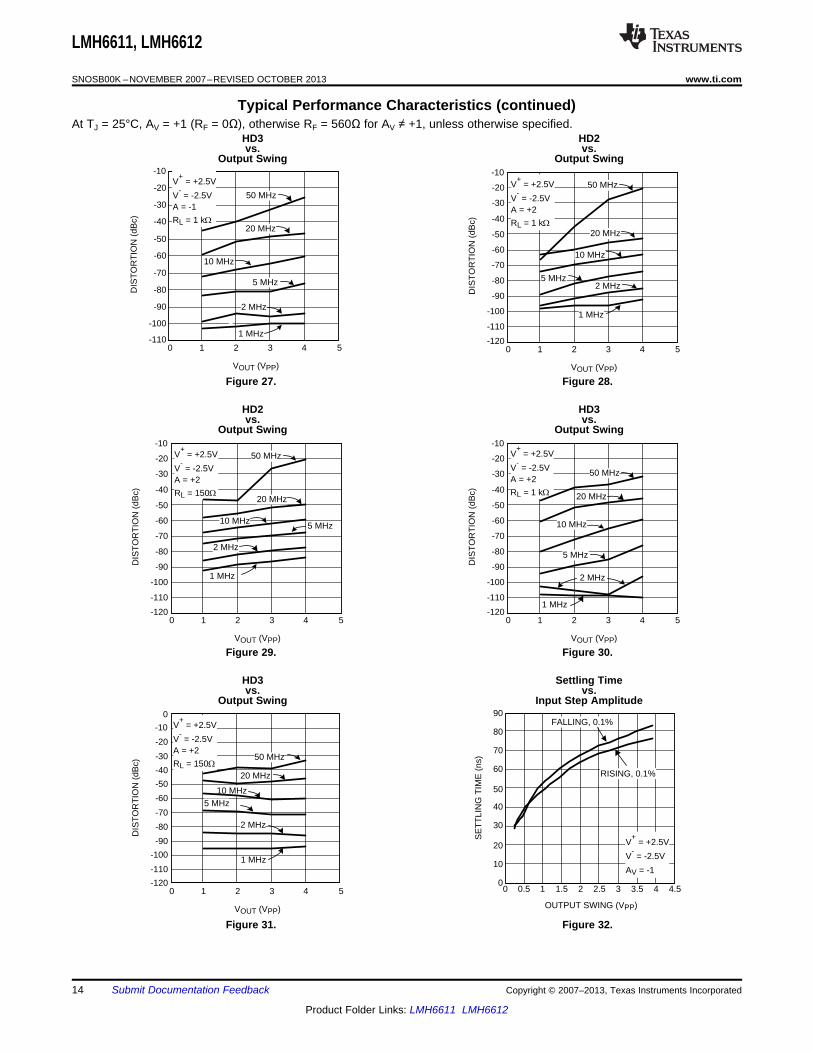
Typical Performance Characteristics (continued)At TJ = 25°C, AV = +1 (RF = 0Ω), otherwise RF = 560Ω for AV ≠ +1, unless otherwise specified.
HD3 HD2vs. vs.
Output Swing Output Swing
Figure 27. Figure 28.
HD2 HD3vs. vs.
Output Swing Output Swing
Figure 29. Figure 30.
HD3 Settling Timevs. vs.
Output Swing Input Step Amplitude
Figure 31. Figure 32.
14 Submit Documentation Feedback Copyright © 2007–2013, Texas Instruments Incorporated
Product Folder Links: LMH6611 LMH6612

-0.5 0.0 0.5 1.0 1.5 2.0 2.5 3.0 3.5 4.0-0.6
-0.5
-0.4
-0.3
-0.2
-0.1
0.0
0.1
VO
S (
mV
)
VCM (V)
125°C
-40°C
25°C
VS = 5V
0 2 4 6 8 10 12
VS (V)
-0.5
-0.4
-0.3
-0.2
-0.1
0
0.1
0.2
VO
S (
mV
)
-40°C
25°C
125°C
V- = -0.5V
VS = V+ - V
-
VCM = 0V
-2.5 -2.0 -1.5 -1.0 -0.5 0 0.5 1.0 1.5 2.0 2.5-6.0
-4.0
-2.0
0
2.0
4.0
6.0
VO
S (
mV
)
VOUT (V)
V+ = +2.5V
V- = -2.5V
RL = 1 k:
125°C
-40°C 25°C
-2.5 -2.0 -1.5 -1.0 -0.5 0 0.5 1.0 1.5 2.0 2.5-6.0
-4.0
-2.0
0
2.0
4.0
6.0
VO
S (
mV
)
VOUT (V)
V+ = +2.5V
V- = -2.5V
RL = 150:
125°C
-40°C 25°C
0 0.5 1 1.5 2 2.5 3 3.5 4 4.50
20
40
60
80
100
120
140
SE
TT
LIN
G T
IME
(ns
)
OUTPUT SWING (VPP)
FALLING, 0.01%
RISING, 0.01%
V+ = +2.5V
V- = -2.5V
AV = -1
10 1k 100k 10M
FREQUENCY (Hz)
1
10
100
1000
1M10k100
VO
LTA
GE
NO
ISE
(nV
/H
z)
1
10
100
1000
CU
RR
EN
T N
OIS
E (
pA/
Hz)
VOLTAGE NOISE
CURRENT NOISE
V+ = +2.5V
V- = -2.5V
LMH6611, LMH6612
www.ti.com SNOSB00K –NOVEMBER 2007–REVISED OCTOBER 2013
Typical Performance Characteristics (continued)At TJ = 25°C, AV = +1 (RF = 0Ω), otherwise RF = 560Ω for AV ≠ +1, unless otherwise specified.
Settling Time Input Noisevs. vs.
Input Step Amplitude Frequency
Figure 33. Figure 34.
VOS VOSvs. vs.
VOUT VOUT
Figure 35. Figure 36.
VOS VOSvs. vs.VCM VS
Figure 37. Figure 38.
Copyright © 2007–2013, Texas Instruments Incorporated Submit Documentation Feedback 15
Product Folder Links: LMH6611 LMH6612

2 3 4 5 6 7 8 9 10 11 12150
100
50
0
50
100
150
VO
UT (
mV
)
VS (V)
VOLTAGE VOUT IS
BELOW V+ SUPPLY
VOLTAGE VOUT IS
ABOVE V- SUPPLY
RL = 1 k: to MID-RAIL
125°C25°C-40°C
2 3 4 5 6 7 8 9 10 11 12500
400
300
200
100
0
100
200
300
400
500
VO
UT (
mV
)
VS (V)
VOLTAGE VOUT IS
BELOW V+ SUPPLY
VOLTAGE VOUT IS
ABOVE V- SUPPLY
RL = 150: to MID-RAIL
-40°C 25°C 125°C
0 2 4 6 8 10 12-6.6
-6.4
-6.2
-6.0
-5.8
-5.6
-5.4
-5.2
-5.0
-4.8
-4.6
I BIA
S (P
A)
VS (V)
V- = -0.5
VS = V+ - V
-
VCM = 0V
25°C125°C
-40°C
4.24.0
3.8
3.6
3.43.2
3.02.8
2.6
2.4
2.22.0
1.81.6
I S (
mA
)
0 2 4 6 8 10 12
VS (V)
125°C
25°C
-40°C
V- = -0.5
VS = V+ - V
-
VCM = 0.5V
-150 -100 -50 0 50 100 150
IOUT (mA)
-1.2
-1.0
-0.8
-0.6
-0.4
-0.2
0
0.2
0.4
VO
S (
mV
)
V+ = +2.5V
V- = -2.5V
-40°C
25°C
125°C
-1.0 -0.6 -0.2 0.2 0.6 1.0-0.8 -0.4 Vos (mv) 0.4 0.8
0
0.5
1.0
1.5
2.0
2.5
3.0
LMH6611, LMH6612
SNOSB00K –NOVEMBER 2007–REVISED OCTOBER 2013 www.ti.com
Typical Performance Characteristics (continued)At TJ = 25°C, AV = +1 (RF = 0Ω), otherwise RF = 560Ω for AV ≠ +1, unless otherwise specified.
VOSvs.IOUT VOS Distribution
Figure 39. Figure 40.
IB ISvs. vs.VS VS
Figure 41. Figure 42.
VOUT VOUTvs. vs.VS VS
Figure 43. Figure 44.
16 Submit Documentation Feedback Copyright © 2007–2013, Texas Instruments Incorporated
Product Folder Links: LMH6611 LMH6612

10 1k 100k 100M
FREQUENCY (Hz)
0
30
80
120
-PS
RR
(dB
)
10M100
110
100
60
50
10
1M10k
90
70
40
20
V+ = +2.5V
V- = -2.5V
V+ = +5V
V- = -5V V
+ = +1.5V
V- = -1.5V
VIN = 225 mVPP
RF = 560:
LMH6611
-
+
VO
0.1 PF 1000 PFRF
560:
RG
560:
0.1 PF 1000 PF
CABLE
a
0.1 PF
50:
+
1000 PF
-
50:3
4 6
2
VIN
-+
-+
1
V+
V-
10 100 1M 100M0
30
50
90
110
+P
SR
R (
dB)
FREQUENCY (Hz)
1k 10k 100k 10M
10
20
40
60
70
100
80
V+ = +2.5V
V- = -2.5V
V+ = +5V
V- = -5V
V+ = +1.5V
V- = -1.5V
VIN = 225 mVPP
RF = 560:
LMH6611-
+
0.1 PF 1000 PF
VO
0.1 PF 1000 PF
CABLE
a
0.1 PF
1000 PF50:
50:
VIN
RF
560:RG
560:
+ -
+
-
V+
V-
2 3 4 5 6 7 8 9 10 11 1270
65
60
55
50
45
40
35
30
25
20
VO
UT (
mV
)
VS (V)
VOLTAGE VOUT IS
ABOVE V- SUPPLY
V- = 0V
RL = 150: TO GND
125°C
-40°C
25°C
0.0001 0.01 1 100
FREQUENCY (MHz)
0.001
1
100
OU
TP
UT
IMP
ED
AN
CE
(:
)
100.10.001
10
0.01
0.1
V+ = +2.5V
V- = -2.5V
LMH6611, LMH6612
www.ti.com SNOSB00K –NOVEMBER 2007–REVISED OCTOBER 2013
Typical Performance Characteristics (continued)At TJ = 25°C, AV = +1 (RF = 0Ω), otherwise RF = 560Ω for AV ≠ +1, unless otherwise specified.
VOUT Closed Loop Output Impedancevs. vs.VS Frequency AV = +1
Figure 45. Figure 46.
+PSRRvs.
Circuit for Positive (+) PSRR Measurement Frequency
Figure 47. Figure 48.
−PSRRvs.
Circuit for Negative (−) PSRR Measurement Frequency
Figure 49. Figure 50.
Copyright © 2007–2013, Texas Instruments Incorporated Submit Documentation Feedback 17
Product Folder Links: LMH6611 LMH6612

50 m
V/D
IV
12.5 ns/DIV
V+ = +5V
V- = -5V
A = +1
VOUT = 0.2V
RL = 1 k:
50 m
V/D
IV
12.5 ns/DIV
V+ = +1.5V
V- = -1.5V
A = -1
RF = 560:
VOUT = 0.2V
RL = 1 k:
50 m
V/D
IV
12.5 ns/DIV
V+ = +1.5V
V- = -1.5V
A = +1
VOUT = 0.2V
RL = 1 k:
50 m
V/D
IV
12.5 ns/DIV
V+ = +2.5V
V- = -2.5V
A = +1
VOUT = 0.2V
RL = 1 k:
100k 1M 10M 100M
FREQUENCY (Hz)
-110
-100
-90
-80
-70
-60
-50
-40
CR
OS
ST
ALK
(dB
)
V+ = +2.5V
V- = -2.5V
A = +1
RL = 1 k:
VOUT = 2 VPP
140
0.0001 0.01 1 100
FREQUENCY (MHz)
0
40
80
CM
RR
(dB
)
100.10.001
120
100
60
20
V+ = +2.5V
V- = -2.5V
LMH6611, LMH6612
SNOSB00K –NOVEMBER 2007–REVISED OCTOBER 2013 www.ti.com
Typical Performance Characteristics (continued)At TJ = 25°C, AV = +1 (RF = 0Ω), otherwise RF = 560Ω for AV ≠ +1, unless otherwise specified.
CMRR Crosstalkvs. vs.
Frequency Frequency
Figure 51. Figure 52.
Small Signal Step Response Small Signal Step Response
Figure 53. Figure 54.
Small Signal Step Response Small Signal Step Response
Figure 55. Figure 56.
18 Submit Documentation Feedback Copyright © 2007–2013, Texas Instruments Incorporated
Product Folder Links: LMH6611 LMH6612

50 m
V/D
IV
12.5 ns/DIV
V+ = +5V
V- = -5V
A = +2
RF = 560:
VOUT = 0.2V
RL = 150:
500
mV
/DIV
12.5 ns/DIV
V+ = +2.5V
V- = -2.5V
A = +1
VOUT = 2V
RL = 1 k:
50 m
V/D
IV
12.5 ns/DIV
V+ = +1.5V
V- = -1.5V
A = +2
RF = 560:
VOUT = 0.2V
RL = 150:
50 m
V/D
IV
12.5 ns/DIV
V+ = +2.5V
V- = -2.5V
A = +2
RF = 560:
VOUT = 0.2V
RL = 150:
50 m
V/D
IV
12.5 ns/DIV
V+ = +2.5V
V- = -2.5V
A = -1
RF = 560:
VOUT = 0.2V
RL = 1 k:
50 m
V/D
IV
12.5 ns/DIV
V+ = +5VV- = -5VA = -1
RF = 560:
VOUT = 0.2V
RL = 1 k:
LMH6611, LMH6612
www.ti.com SNOSB00K –NOVEMBER 2007–REVISED OCTOBER 2013
Typical Performance Characteristics (continued)At TJ = 25°C, AV = +1 (RF = 0Ω), otherwise RF = 560Ω for AV ≠ +1, unless otherwise specified.
Small Signal Step Response Small Signal Step Response
Figure 57. Figure 58.
Small Signal Step Response Small Signal Step Response
Figure 59. Figure 60.
Small Signal Step Response Large Signal Step Response
Figure 61. Figure 62.
Copyright © 2007–2013, Texas Instruments Incorporated Submit Documentation Feedback 19
Product Folder Links: LMH6611 LMH6612

-2.5 -2.0 -1.5 -1.0 -0.5 0 0.5 1.0 1.5 2.0 2.50
500
1000
1500
2000
2500
3000
3500
4000
I S (P
A)
VDISABLE (V)
V+ = +2.5V
V- = -2.5V
125°C
-40°C
25°C
500
mV
/DIV
12.5 ns/DIV
V+ = +2.5V
V- = -2.5V
A = +2
RF = 560:
VOUT = 2V
RL = 150:
1V/D
IV
25 ns/DIV
VOUT
VIN
V+ = +5V
V- = -5V
AV = +5
RF = 604:
RL = 1 k:
LMH6611, LMH6612
SNOSB00K –NOVEMBER 2007–REVISED OCTOBER 2013 www.ti.com
Typical Performance Characteristics (continued)At TJ = 25°C, AV = +1 (RF = 0Ω), otherwise RF = 560Ω for AV ≠ +1, unless otherwise specified.
Large Signal Step Response Overload Recovery Response
Figure 63. Figure 64.
ISvs.
VDISABLE
Figure 65.
20 Submit Documentation Feedback Copyright © 2007–2013, Texas Instruments Incorporated
Product Folder Links: LMH6611 LMH6612

2V/D
IV
25 ns/DIV
VOUT
VIN
V+ = +2.5V
V- = -2.5V
AV = +1
RF = 560:
RL = 1 k:
LMH6611, LMH6612
www.ti.com SNOSB00K –NOVEMBER 2007–REVISED OCTOBER 2013
APPLICATION INFORMATION
The LMH6611 and LMH6612 are based on proprietary VIP10 dielectrically isolated bipolar process. This devicefamily architecture features the following:• Complimentary bipolar devices with exceptionally high ft (∼8 GHz) even under low supply voltage (2.7V) and
low bias current.• Common emitter push-push output stage. This architecture allows the output to reach within millivolts of either
supply rail.• Consistent performance with little variation from any supply voltage (2.7V - 11V) for the most important
specifications (BW, SR, IOUT, for example.)• Significant power saving compared to competitive devices on the market with similar performance.
With 3V supplies and a common mode input voltage range that extends beyond either supply rail, the LMH6611is well suited to many low voltage/low power applications. Even with 3V supplies, the −3 dB BW (at AV = +1) istypically 305 MHz.
The LMH6611 and LMH6612 are designed to avoid output phase reversal. With input overdrive, the output iskept near the supply rail (or as close to it as mandated by the closed loop gain setting and the input voltage).Figure 66 shows the input and output voltage when the input voltage significantly exceeds the supply voltages.
Figure 66. Input and Output Shown with CMVR Exceeded
If the input voltage range is exceeded by more than a diode drop beyond either rail, the internal ESD protectiondiodes will start to conduct. The current flow in these ESD diodes should be externally limited.
SHUTDOWN CAPABILITY AND TURN ON/OFF BEHAVIORThe LMH6611 can be shutdown by connecting the DISABLE pin to a voltage 0.5V below the supply midpointwhich will reduce the supply current to typically 120 µA. The DISABLE pin is “active low” and can be connectedthrough a resistor to V+ or left floating for normal operation. Shutdown is specified when the DISABLE pin is 0.5Vbelow the supply midpoint at any operating supply voltage and temperature. Typical turn on time is 20 ns and theturn off time is 60 ns.
In the shutdown mode, essentially all internal device biasing is turned off in order to minimize supply current flowand the output goes into high impedance mode. During shutdown, the input stage has an equivalent circuit asshown in Figure 67.
Copyright © 2007–2013, Texas Instruments Incorporated Submit Documentation Feedback 21
Product Folder Links: LMH6611 LMH6612

1 10 100 1000
FREQUENCY (MHz)
-6
-3
0
3
NO
RM
ALI
ZE
D G
AIN
(dB
)
RF = RG = 665:
RF = RG = 1000:
V+ = +2.5V
V- = -2.5V
VOUT = 0.2V
RL = 1 k:
D1
D2D3
D4
NON-INVERTING INPUT
INVERTING INPUT
RS
50:
LMH6611, LMH6612
SNOSB00K –NOVEMBER 2007–REVISED OCTOBER 2013 www.ti.com
Figure 67. Input Equivalent Circuit During Shutdown
When the LMH6611 is shutdown, there may be current flow through the internal diodes shown, caused by inputpotential, if present. This current may flow through the external feedback resistor and result in an apparent outputsignal. In most shutdown applications the presence of this output is inconsequential. However, if the output is“forced” by another device, the other device will need to conduct the current described in order to maintain theoutput potential.
To keep the output at or near ground during shutdown when there is no other device to hold the output low, aswitch using a transistor can be used to shunt the output to ground.
SELECTION OF RF AND EFFECT ON STABILITY AND PEAKINGThe peaking of the LMH6611 depends on the value of the RF. From the graph shown in Figure 68, as the RFvalue increases, the peaking increases.
For AV = 2, at RF = 1 kΩ, the −3 dB bandwidth is 113 MHz and peaking is about 0.6 dB whereas at RF = 665Ω,the −3 dB bandwidth is about 110 MHz and peaking is 0 dB. RF and the input capacitance form a pole in theamplifier’s response. If the time constant is too big, it will cause peaking and ringing.
Except for AV = 1 when RF should be 0Ω, across all other gain settings it is recommended that RF remainbetween 500Ω and 1 kΩ to ensure optimum performance.
Figure 68. Closed Loop Gain vs. Frequency and RF = RG
22 Submit Documentation Feedback Copyright © 2007–2013, Texas Instruments Incorporated
Product Folder Links: LMH6611 LMH6612

LMH6611, LMH6612
www.ti.com SNOSB00K –NOVEMBER 2007–REVISED OCTOBER 2013
RF = RG f −3 dB (MHz) Peaking (dB)665 110 01000 113 0.6
MINIMIZING NOISEWith a low input voltage noise of 10 nV/√Hz and an input current noise of 2 pA√Hz the LMH6611 and LMH6612are suitable for high accuracy applications. Still being able to reduce the frequency band of operation of thevarious noise sources (that is, op amp noise voltage, resistor thermal noise, input noise current) can furtherimprove the noise performance of a system. In a non-inverting amplifier configuration inserting a capacitor, CG, inseries with the gain setting resistor, RG, will reduce the gain of the circuit below frequency, f = 1/2πRGCG. Thiscan be set to reduce the contribution of noise from the 1/f region. Alternatively applying a feedback capacitor, CF,in parallel with the feedback resistor, RF, will introduce a pole into your system at f = 1/2πRFCF and create a lowpass filter. This filter can be set to reduce high frequency noise and harmonics. Finally remember to keep resistorvalues as small as possible for a given application in order to reduce resistor thermal noise.
POWER SUPPLY BYPASSSince the LMH6611 and LMH6612 are wide bandwidth amplifiers, proper power supply bypassing is critical foroptimum performance. Improper power supply bypassing can result in large overshoot, ringing or oscillation. 0.1μF capacitors should be connected from the supply pins, V+ and V−, to ground, as close to the device as ispractical. Additionally, a 10 μF electrolytic capacitor should be connected from both supply pins to groundreasonably close to the device. Finally, near the device a 0.1 μF ceramic capacitor between the supplies willprovide the best harmonic distortion performance.
INTERFACING HIGH PERFORMANCE OP AMPS WITH ADCsThese amplifiers are designed for ease of use in a wide range of applications requiring high speed, low supplycurrent, low noise, and the ability to drive complex ADC and video loads.
The source that drives the modern high resolution analog-to-digital converters (ADCs) sees a high frequency ACload and a DC load of a few hundred ohms or more. Thus, a high performance op amp with high inputimpedance of a few mega ohms and low output impedance would be an ideal choice as an input ADC driver.The LMH6611/LMH6612 have the low output impedance of 0.07Ω at f = 1 MHz. The ADC driver acts as a bufferand a low pass filter to reduce the overall system noise. To utilize the full dynamic range of the ADC, the ADCinput has to be driven to full scale input voltage.
As signals travel through the traces of a printed circuit board (PCB) and long cables, system noise accumulatesin the signals and a differential ADC rejects any signals noise that appears as a common mode voltage. Thereare a couple of advantages to using differential signals rather than single-ended signals. First, differential signalsdouble the dynamic range of the ADC and second, they offer better harmonic distortion performance. There areseveral ways to produce differential signals from a dual op amp configuration. One method is to utilize the single-ended to differential conversion technique and the other is the differential to differential conversion technique.The first method requires a single input source and the second method requires differential input source.
A real world input source can have non-ideal impedance thus the buffer amplifier, with very low outputimpedance, is required to drive the input of the ADC. To minimize the droop in the input voltage, external shuntcapacitance (CL) should be about ten times larger than the internal input capacitance of the ADC and externalseries resistance (RL) should be large enough to maintain the phase delay at the output of the op amp andhence maintain the stability (See Figure 69). Most applications benefit from the inclusion of a series isolationresistor connected between the op amp output and ADC input. This series resistor helps to limit the outputcurrent of the op amp. The value chosen for this series resistor is very important, as a higher value will increasethe load impedance seen by the op amp and improve the total harmonic distortion (THD) performance of the opamp; however, the ADC prefers a low impedance source driving it. Thus, the optimum value for this seriesresistor must be found so that it will offer the best performance in terms of THD, SNR and SFDR of the combinedop amp and ADC.
Copyright © 2007–2013, Texas Instruments Incorporated Submit Documentation Feedback 23
Product Folder Links: LMH6611 LMH6612

=R2
GAIN -R1
=1
2Sx 1
R2 x R5 x C2 x C5
´¶0
SINAD = 20 * LOG + 10 10 10THD
10-SNR
LMH6611, LMH6612
SNOSB00K –NOVEMBER 2007–REVISED OCTOBER 2013 www.ti.com
Important Specifications of Op Amp and ADCWhen interfacing an ADC with an op amp it is imperative to understand the specifications that are important toget the expected performance results. Modern ADC AC specifications such as THD, SNR, settling time andSFDR are critical for filtering, test and measurement, video and reconstruction applications. The highperformance op amp’s settling time, THD, and noise performance must be better than that of the ADC it is drivingto maintain the proper system accuracy with minimal or no error.
Some system applications require low THD, low SFDR and wide dynamic range (SNR), whereas some systemapplications require high SNR and they may sacrifice THD and SFDR to focus on the noise performance.
Noise is a very important specification for both the op amp and the ADC. There are three main sources of noisethat contribute to the overall performance of the ADC: Quantization noise, noise generated by the ADC itself(particularly at higher frequencies) and the noise generated by the application circuit. The impedance of the inputsource affects the noise performance of the op amp. Theoretically, an ADC’s signal to noise ratio (SNR) can befound from the equation:
SNR (in dB) = 6.02*N+1.72 (1)
where N is the resolution of the ADC. For example, according to this equation a 12-bit ADC has an SNR of 74dB. However, the practical SNR number would be about 72 dB. In order to achieve better SNR, the ADC drivernoise should be as small as possible. The LMH6611/LMH6612 have the low voltage noise of only 10 nV/√Hz.
The combined settling time of the op amp and the ADC must be within 1 LSB. The 0.01% settling time of theLMH6611/LMH6612 is 100 ns.
The ADC driver’s THD should be inherently lower than that of the ADC. The LMH6611/LMH6612 have an SFDRof 96 dBc at 2 VPP output and 1 MHz input frequency.
Signal to Noise and Distortion (SINAD) is a parameter which is the combination of the SNR and THDspecifications. SINAD is defined as the RMS value of the output signal to the RMS value of all of the otherspectral components below half the clock frequency, including harmonics but excluding DC. It can be calculatedfrom SNR and THD according to the equation:
(2)
Because SINAD compares all undesired frequency components with the input frequency, it is an overall measureof an ADC’s dynamic performance. The following sections will discuss the three different ADC driverarchitectures in detail.
SINGLE TO SINGLE ADC DRIVERThis architecture has a single-ended input source connected to the input of the op amp and the single-endedoutput of the op amp is then fed to the single-ended input of the ADC. The low noise of only 10 nV/√Hz and awide bandwidth of 345 MHz make the LMH6611 an excellent choice for driving the 12-bit ADC121S101 500KSPS to 1 MSPS ADC, which has a successive approximation architecture with internal sample and holdcircuits. Figure 67 shows the schematic of the LMH6611 in a 2nd order multiple-feedback with gain of −1(inverting) configuration, driving an ADC121S101. The inverting configuration is preferred over the non-invertingconfiguration, as it offers more linear output response. Table 1 shows the performance data of the LMH6611combined with the ADC121S101. The ADC driver’s cutoff frequency of 500 kHz is found from the equation:
(3)
The op amp’s gain is set by the equation:
(4)
24 Submit Documentation Feedback Copyright © 2007–2013, Texas Instruments Incorporated
Product Folder Links: LMH6611 LMH6612

LMH6611 ADC121S101
0.1 PF 10 PF0.1 PF 10 PF
0.1 PF
V+
0.01 PF R614.3 k:
0.1 PF1 PF
GND
5V
R5
1.24 k:
C2
1 nF
C5
150 pF
R2
549:
V+
-
+
RL
22:
CL
390 pF
R1
549:IN
1 PF
V+
R7
14.3 k:
5.6 PFU1
LMH6611, LMH6612
www.ti.com SNOSB00K –NOVEMBER 2007–REVISED OCTOBER 2013
Figure 69. Single to Single ADC Driver
Table 1. Performance of the LMH6611 Combined with the ADC121S101Amplifier SINAD SNR THD SFDR ENOB Notes
Output/ADC Input (dB) (dB) (dB) (dBc)4 70.2 71.6 −75.7 77.6 11.4 ADC121S101 @ f = 200 kHz
When the op amp and the ADC are using the same supply, it is important that both devices are well bypassed. A0.1 µF ceramic capacitor and a 10 µF tantalum capacitor should be located as close as possible to each supplypin. A sample layout is shown in Figure 70. The 0.1 µF capacitors (C13 and C6) and the 10 µF capacitors (C11and C5) are located very close to the supply pins of the LMH6611 and the ADC121S101.
The following are recommendations for the design of PCB layout in order to obtain the optimum high frequencyperformance:• Place ADC and amplifier as close together as possible.• Put the supply bypassing capacitors as close as possible to the device (<1”).• Utilize surface mount instead of through-hole components and ground and power planes.• Keep the traces short where possible.• Use terminated transmission lines for long traces.
Copyright © 2007–2013, Texas Instruments Incorporated Submit Documentation Feedback 25
Product Folder Links: LMH6611 LMH6612

ADC121S625
0.1 PF 10 PF
V+
33:
V+
560:220 pF
560:
-
+
0.1 PF 10 PF
V+
V+
560:
560: 33:
560:
220 pF
560:
INPUT
10 PF
-
+LMH6612
LMH6612
0.1 PF 10 PF
V+
U1
U2
LMH6611, LMH6612
SNOSB00K –NOVEMBER 2007–REVISED OCTOBER 2013 www.ti.com
Figure 70. LMH6611 and ADC121S101 Layout
SINGLE-ENDED TO DIFFERENTIAL ADC DRIVERThe single-ended to differential ADC driver in Figure 68 utilizes an LMH6612 dual op amp to buffer a single-ended source to drive an ADC with differential inputs. One of the op amps is configured as a unity gain bufferthat drives the inverting (IN−) input of the op amp U2 and non-inverting (IN+) input of the ADC121S625. U2inverts the input signal and drives the inverting input of the ADC121S625. The ADC driver is configured for again of +2 to reduce the noise without sacrificing THD performance. The common mode voltage of 2.5V is set upat the non-inverting inputs of both op amps U1 and U2. This configuration produces differential ±2.5 VPP outputsignals, when the single-ended input signal of 0 to VREF is AC coupled into the non-inverting terminal of the opamp and each non-inverting terminal of the op amp is biased at the mid-scale of 2.5V. The two output RC anti-aliasing filters are used between both the outputs of U1 and U2 and the input of the ADC121S625 to minimizethe effect of undesired high frequency noise coming from the input source. Each RC filter has the cutofffrequency of approximately 22 MHz.
Figure 71. Single-Ended to Differential ADC Driver
26 Submit Documentation Feedback Copyright © 2007–2013, Texas Instruments Incorporated
Product Folder Links: LMH6611 LMH6612

LMH6612
0.1 PF 10 PF
0.1 PF
V+
1.24 k:
1 nF
150 pF
549:
V+
-
+
22:
390 pF
14.3 k:
5.6 PF
14.3 k:
1 PF 549:
ADC121S705
0.1 PF 10 PF
V+
LMH6612
0.1 PF 10 PF
0.1 PF
V+
1.24 k:
1 nF
150 pF
549:
V+
-
+
14.3 k:
5.6 PF
14.3 k:
1 PF 549: 22:
390 pF
+IN
-IN
LMH6611, LMH6612
www.ti.com SNOSB00K –NOVEMBER 2007–REVISED OCTOBER 2013
The performance of the LMH6612 with the ADC121S625 is shown in Table 2.
Table 2. Performance of the LMH6612 Combined with the ADC121S625Amplifier SINAD SNR THD SFDR ENOB Notes
Output/ADC Input (dB) (dB) (dB) (dBc)2.5 68.8 69 −81.5 75.1 11.2 ADC121S625 @ f = 20 kHz
DIFFERENTIAL TO DIFFERENTIAL ADC DRIVERThe LMH6612 dual op amp can be configured as a differential to differential ADC driver to buffer a differentialsource to a differential input ADC as shown in Figure 72. The differential to differential ADC driver can be formedusing two single to single ADC drivers. Each output from these drivers goes to a separate input of the differentialADC. Here, each single to single ADC driver uses the same components and is configured for a gain of -1(inverting).
Figure 72. Differential to Differential ADC Driver
The following table summarizes the performance of the LMH6612 combined with the ADC121S625 at twodifferent frequencies. In order to utilize the full dynamic range of the ADC, the maximum input of 2.5 VPP isapplied to the ADC input. Figure 73 shows the FFT plot of the LMH6612 and ADC121S625 combination tested atf = 20 kHz input frequency.
Copyright © 2007–2013, Texas Instruments Incorporated Submit Documentation Feedback 27
Product Folder Links: LMH6611 LMH6612

LMH6611, LMH6612
SNOSB00K –NOVEMBER 2007–REVISED OCTOBER 2013 www.ti.com
Table 3. Performance of the LMH6612 Combined with the ADC121S625Amplifier SINAD SNR THD SFDR ENOB Notes
Output/ADC Input (dB) (dB) (dB) (dBc)2.5 72.2 72.3 −87.7 92.1 11.7 ADC121S625 @ f = 20 kHz2.5 72.2 72.2 −87.8 90.8 11.7 ADC121S625 @ f = 200 kHz
Figure 73. The FFT Plot of Differential to Differential ADC Driver
28 Submit Documentation Feedback Copyright © 2007–2013, Texas Instruments Incorporated
Product Folder Links: LMH6611 LMH6612

+
-
VIN
R1
RG RF
VOUTLMH6611
R2
V+
V+
LMH6611, LMH6612
www.ti.com SNOSB00K –NOVEMBER 2007–REVISED OCTOBER 2013
DC LEVEL SHIFTINGOften a signal must be both amplified and level shifted while using a single supply for the op amp. The circuit inFigure 74 can do both of these tasks. The procedure for specifying the resistor values is as follows.1. Determine the input voltage.2. Calculate the input voltage midpoint, VINMID = VINMIN + (VINMAX – VINMIN)/2.3. Determine the output voltage needed.4. Calculate the output voltage midpoint, VOUTMID = VOUTMIN + (VOUTMAX – VOUTMIN)/2.5. Calculate the gain needed, gain = (VOUTMAX – VOUTMIN)/(VINMAX – VINMIN)6. Calculate the amount the voltage needs to be shifted from input to output, ΔVOUT = VOUTMID – gain x VINMID.7. Set the supply voltage to be used.8. Calculate the noise gain, noise gain = gain + ΔVOUT/VS.9. Set RF.10. Calculate R1, R1 = RF/gain.11. Calculate R2, R2 = RF/(noise gain-gain).12. Calculate RG, RG= RF/(noise gain – 1).
Check that both the VIN and VOUT are within the voltage ranges of the LMH6611.
Figure 74. DC Level Shifting
The following example is for a VIN of 0V to 1V with a VOUT of 2V to 4V.1. VIN = 0V to 1V2. VINMID = 0V + (1V – 0V)/2 = 0.5V3. VOUT = 2V to 4V4. VOUTMID = 2V + (4V – 2V)/2 = 3V5. Gain = (4V – 2V)/(1V – 0V) = 26. ΔVOUT = 3V – 2 x 0.5V = 27. For the example the supply voltage will be +5V.8. Noise gain = 2 + 2/5V = 2.49. RF = 2 kΩ10. R1 = 2 kΩ/2 = 1 kΩ11. R2 = 2 kΩ/(2.4-2) = 5 kΩ12. RG = 2 kΩ/(2.4 – 1) = 1.43 kΩ
Copyright © 2007–2013, Texas Instruments Incorporated Submit Documentation Feedback 29
Product Folder Links: LMH6611 LMH6612

+
-
LMH6611
1 k:
51:
51:
0.1:
0A to 1A
1 k:
+5V
0.1 PF 1 PF
0.1 PF 1 PF
820 pF
1.02 k:
62 pF
1.02 k:
V+
-
+
V-
510:
OUTPUT
0.1 PF 1 PF
0.1 PF 1 PF
330 pF
1.05 k:
150 pF
V+
-
+
523:
V-
INPUT
1.05 k:
LMH6612LMH6612
LMH6611, LMH6612
SNOSB00K –NOVEMBER 2007–REVISED OCTOBER 2013 www.ti.com
4th ORDER MULTIPLE FEEDBACK LOW-PASS FILTERFigure 75 shows the LMH6612 used as the amplifier in a multiple feedback low pass filter. This filter is set up tohave a gain of +1 and a −3 dB point of 1 MHz. Values can be determined by using the WEBENCH® Active FilterDesigner found at www.ti.com/amplifiers
Figure 75. 4th Order Multiple Feedback Low-Pass Filter
CURRENT SENSE AMPLIFIER AND OPTIMIZING ACCURACY IN PRECESION APPLICATIONSWith it’s rail-to-rail output capability, low VOS, and low IB the LMH6611 is an ideal choice for a current senseamplifier application. Figure 76 shows the schematic of the LMH6611 set up in a low-side sense configurationwhich provides a conversion gain of 2V/A. Voltage error due to VOS can be calculated to be VOS x (1 + RF/RG) or1.5 mV x 21 = 31.5 mV. Voltage error due to IO is IO x RF or 0.5 µA x 1 kΩ = 0.5 mV. Hence worst case totalvoltage error is 12.6 mV + 0.5 mV or 13.1 mV which translates into a current error of 13.1 mV/(2 V/A) = 6.55 mA.
This circuit employs DC source resistance matching at the two input terminals in order to minimize the output DCerror caused by input bias current. Another technique to reduce output offset in a non-inverting amplifierconfiguration is to introduce a DC offset current into the inverting input of the amplifier. To ensure minimal impacton frequency response be sure to inject the DC offset current through large resistors. Conversely if optimizing aninverting amplifier configuration simply apply offset adjustment to the non-inverting input.
Figure 76. Current Sense Amplifier
30 Submit Documentation Feedback Copyright © 2007–2013, Texas Instruments Incorporated
Product Folder Links: LMH6611 LMH6612

NOISE GAIN (NG)
OP AMP OPENLOOP GAIN
I-V GAIN (:)
GA
IN (
dB)
0 dB
FREQUENCY
1 + sRF (CT + CF)
1 + sRFCF
1 +CIN
CF
GBWPfz #
1
2SRFCTfP =
1
2SRFCF
2SRFCT
Where, fZ 1# and fP = 2SRFCF
1
NG = 1 + sRF (CT + CF)
1 + sCFRF
+
-
CPD CINLMH6611
RF
CF
VS
LMH6611, LMH6612
www.ti.com SNOSB00K –NOVEMBER 2007–REVISED OCTOBER 2013
TRANSIMPEDANCE AMPLIFIERBy definition, a photodiode produces either a current or voltage output from exposure to a light source. ATransimpedance Amplifier (TIA) is utilized to convert this low-level current to a usable voltage signal. The TIAoften will need to be compensated to insure proper operation.
Figure 77. Photodiode Modeled with Capacitance Elements
Figure 77 shows the LMH6611 modeled with photodiode and the internal op amp capacitances. The LMH6611allows circuit operation of a low intensity light due to its low input bias current by using larger values of gain (RF).The total capacitance (CT) on the inverting terminal of the op amp includes the photodiode capacitance (CPD) andthe input capacitance of the op amp (CIN). This total capacitance (CT) plays an important role in the stability ofthe circuit. The noise gain of this circuit determines the stability and is defined by:
(5)
(6)
Figure 78. Bode Plot of Noise Gain Intersecting with Op Amp Open Loop Gain
Figure 78 shows the bode plot of the noise gain intersecting the op amp open loop gain. With larger values ofgain, CT and RF create a zero in the transfer function. At higher frequencies the circuit can become unstable dueto excess phase shift around the loop.
A pole at fP in the noise gain function is created by placing a feedback capacitor (CF) across RF. The noise gainslope is flattened by choosing an appropriate value of CF for optimum performance.
Copyright © 2007–2013, Texas Instruments Incorporated Submit Documentation Feedback 31
Product Folder Links: LMH6611 LMH6612

-27
-24
-21
-18
-15
-12
-9
-6
-3
0
3
NO
RM
ALI
ZE
D I-
V G
AIN
(dB
)
1M 10M 100M
FREQUENCY (Hz)
CPD = 330 pF,
CF = 22 pF
CPD = 222 pF,
CF = 18 pF
CPD = 100 pF,
CF = 12 pF
CPD = 22 pF,
CF = 5.6 pF
CPD = 47 pF,
CF = 8 pF
2SRFCTf-3 dB
GBWP=
CF = CT
2SRF(GBWP)
LMH6611, LMH6612
SNOSB00K –NOVEMBER 2007–REVISED OCTOBER 2013 www.ti.com
Theoretical expressions for calculating the optimum value of CF and the expected −3 dB bandwidth are:
(7)
(8)
Equation 8 indicates that the −3 dB bandwidth of the TIA is inversely proportional to the feedback resistor.Therefore, if the bandwidth is important then the best approach would be to have a moderate transimpedancegain stage followed by a broadband voltage gain stage.
Table 4 shows the measurement results of the LMH6611 with different photodiodes having various capacitances(CPD) and a feedback resistance (RF) of 1 kΩ.
Table 4. TIA (Figure 66) Compensation and Performance Results (1)
CPD CT CF CAL CF USED f −3 dB CAL f −3 dB MEAS Peaking(pF) (pF) (pF) (pF) (MHz) (MHz) (dB)22 24 5.42 5.6 29.3 27.1 0.547 49 7.75 8 20.5 21 0.5100 102 11.15 12 14.2 15.2 0.5222 224 20.39 18 9.6 10.7 0.5330 332 20.2 22 7.9 9 0.8
(1) GBWP = 130 MHz, CT = CPD + CIN, CIN = 2 pF, VS = ±2.5V
Figure 79 shows the frequency response for the various photodiodes in Table 4.
Figure 79. Frequency Response for Various Photodiode and Feedback Capacitors
When analyzing the noise at the output of the TIA, it is important to note that the various noise sources (that is,op amp noise voltage, feedback resistor thermal noise, input noise current, photodiode noise current) do not alloperate over the same frequency band. Therefore, when the noise at the output is calculated, this should betaken into account. The op amp noise voltage will be gained up in the region between the noise gain’s zero andpole (fZ and fP in Figure 78). The higher the values of RF and CT, the sooner the noise gain peaking starts andtherefore its contribution to the total output noise will be larger. It is advantageous to minimize CIN by properchoice of op amp or by applying a reverse bias across the diode but this will be at the expense of excess darkcurrent and noise.
32 Submit Documentation Feedback Copyright © 2007–2013, Texas Instruments Incorporated
Product Folder Links: LMH6611 LMH6612

LMH6611, LMH6612
www.ti.com SNOSB00K –NOVEMBER 2007–REVISED OCTOBER 2013
EVALUATION BOARDTI provides the following evaluation board as a guide for high frequency layout and as an aid in device testingand characterization. Many of the datasheet plots were measured with this board:
Device Package Board Part #LMH6611MK SOT LMH730216LMH6612MA SOIC LMH730036
Copyright © 2007–2013, Texas Instruments Incorporated Submit Documentation Feedback 33
Product Folder Links: LMH6611 LMH6612

LMH6611, LMH6612
SNOSB00K –NOVEMBER 2007–REVISED OCTOBER 2013 www.ti.com
REVISION HISTORY
Changes from Revision I (March 2013) to Revision J Page
• Changed layout of National Data Sheet to TI format .......................................................................................................... 33
Changes from Revision J (September 2013) to Revision K Page
• Changed from 0.1 uV/°C to 4 μV/°C ..................................................................................................................................... 3• Changed from 0.1 uV/°C to 4 μV/°C ..................................................................................................................................... 5• Changed from 0.4 uV/°C to 4 μV/°C ..................................................................................................................................... 7
34 Submit Documentation Feedback Copyright © 2007–2013, Texas Instruments Incorporated
Product Folder Links: LMH6611 LMH6612

PACKAGE OPTION ADDENDUM
www.ti.com 28-Feb-2017
Addendum-Page 1
PACKAGING INFORMATION
Orderable Device Status(1)
Package Type PackageDrawing
Pins PackageQty
Eco Plan(2)
Lead/Ball Finish(6)
MSL Peak Temp(3)
Op Temp (°C) Device Marking(4/5)
Samples
LMH6611MK/NOPB ACTIVE SOT-23-THIN DDC 6 1000 Green (RoHS& no Sb/Br)
CU SN Level-1-260C-UNLIM -40 to 125 AX4A
LMH6611MKE/NOPB ACTIVE SOT-23-THIN DDC 6 250 Green (RoHS& no Sb/Br)
CU SN Level-1-260C-UNLIM -40 to 125 AX4A
LMH6611MKX/NOPB ACTIVE SOT-23-THIN DDC 6 3000 Green (RoHS& no Sb/Br)
CU SN Level-1-260C-UNLIM -40 to 125 AX4A
LMH6612MA/NOPB ACTIVE SOIC D 8 95 Green (RoHS& no Sb/Br)
CU SN Level-1-260C-UNLIM -40 to 125 LMH6612MA
LMH6612MAX/NOPB ACTIVE SOIC D 8 2500 Green (RoHS& no Sb/Br)
CU SN Level-1-260C-UNLIM -40 to 125 LMH6612MA
(1) The marketing status values are defined as follows:ACTIVE: Product device recommended for new designs.LIFEBUY: TI has announced that the device will be discontinued, and a lifetime-buy period is in effect.NRND: Not recommended for new designs. Device is in production to support existing customers, but TI does not recommend using this part in a new design.PREVIEW: Device has been announced but is not in production. Samples may or may not be available.OBSOLETE: TI has discontinued the production of the device.
(2) Eco Plan - The planned eco-friendly classification: Pb-Free (RoHS), Pb-Free (RoHS Exempt), or Green (RoHS & no Sb/Br) - please check http://www.ti.com/productcontent for the latest availabilityinformation and additional product content details.TBD: The Pb-Free/Green conversion plan has not been defined.Pb-Free (RoHS): TI's terms "Lead-Free" or "Pb-Free" mean semiconductor products that are compatible with the current RoHS requirements for all 6 substances, including the requirement thatlead not exceed 0.1% by weight in homogeneous materials. Where designed to be soldered at high temperatures, TI Pb-Free products are suitable for use in specified lead-free processes.Pb-Free (RoHS Exempt): This component has a RoHS exemption for either 1) lead-based flip-chip solder bumps used between the die and package, or 2) lead-based die adhesive used betweenthe die and leadframe. The component is otherwise considered Pb-Free (RoHS compatible) as defined above.Green (RoHS & no Sb/Br): TI defines "Green" to mean Pb-Free (RoHS compatible), and free of Bromine (Br) and Antimony (Sb) based flame retardants (Br or Sb do not exceed 0.1% by weightin homogeneous material)
(3) MSL, Peak Temp. - The Moisture Sensitivity Level rating according to the JEDEC industry standard classifications, and peak solder temperature.
(4) There may be additional marking, which relates to the logo, the lot trace code information, or the environmental category on the device.
(5) Multiple Device Markings will be inside parentheses. Only one Device Marking contained in parentheses and separated by a "~" will appear on a device. If a line is indented then it is a continuationof the previous line and the two combined represent the entire Device Marking for that device.

PACKAGE OPTION ADDENDUM
www.ti.com 28-Feb-2017
Addendum-Page 2
(6) Lead/Ball Finish - Orderable Devices may have multiple material finish options. Finish options are separated by a vertical ruled line. Lead/Ball Finish values may wrap to two lines if the finishvalue exceeds the maximum column width.
Important Information and Disclaimer:The information provided on this page represents TI's knowledge and belief as of the date that it is provided. TI bases its knowledge and belief on informationprovided by third parties, and makes no representation or warranty as to the accuracy of such information. Efforts are underway to better integrate information from third parties. TI has taken andcontinues to take reasonable steps to provide representative and accurate information but may not have conducted destructive testing or chemical analysis on incoming materials and chemicals.TI and TI suppliers consider certain information to be proprietary, and thus CAS numbers and other limited information may not be available for release.
In no event shall TI's liability arising out of such information exceed the total purchase price of the TI part(s) at issue in this document sold by TI to Customer on an annual basis.

TAPE AND REEL INFORMATION
*All dimensions are nominal
Device PackageType
PackageDrawing
Pins SPQ ReelDiameter
(mm)
ReelWidth
W1 (mm)
A0(mm)
B0(mm)
K0(mm)
P1(mm)
W(mm)
Pin1Quadrant
LMH6611MK/NOPB SOT-23-THIN
DDC 6 1000 178.0 8.4 3.2 3.2 1.4 4.0 8.0 Q3
LMH6611MKE/NOPB SOT-23-THIN
DDC 6 250 178.0 8.4 3.2 3.2 1.4 4.0 8.0 Q3
LMH6611MKX/NOPB SOT-23-THIN
DDC 6 3000 178.0 8.4 3.2 3.2 1.4 4.0 8.0 Q3
LMH6612MAX/NOPB SOIC D 8 2500 330.0 12.4 6.5 5.4 2.0 8.0 12.0 Q1
PACKAGE MATERIALS INFORMATION
www.ti.com 3-Mar-2017
Pack Materials-Page 1

*All dimensions are nominal
Device Package Type Package Drawing Pins SPQ Length (mm) Width (mm) Height (mm)
LMH6611MK/NOPB SOT-23-THIN DDC 6 1000 210.0 185.0 35.0
LMH6611MKE/NOPB SOT-23-THIN DDC 6 250 210.0 185.0 35.0
LMH6611MKX/NOPB SOT-23-THIN DDC 6 3000 210.0 185.0 35.0
LMH6612MAX/NOPB SOIC D 8 2500 367.0 367.0 35.0
PACKAGE MATERIALS INFORMATION
www.ti.com 3-Mar-2017
Pack Materials-Page 2


IMPORTANT NOTICE
Texas Instruments Incorporated (TI) reserves the right to make corrections, enhancements, improvements and other changes to itssemiconductor products and services per JESD46, latest issue, and to discontinue any product or service per JESD48, latest issue. Buyersshould obtain the latest relevant information before placing orders and should verify that such information is current and complete.TI’s published terms of sale for semiconductor products (http://www.ti.com/sc/docs/stdterms.htm) apply to the sale of packaged integratedcircuit products that TI has qualified and released to market. Additional terms may apply to the use or sale of other types of TI products andservices.Reproduction of significant portions of TI information in TI data sheets is permissible only if reproduction is without alteration and isaccompanied by all associated warranties, conditions, limitations, and notices. TI is not responsible or liable for such reproduceddocumentation. Information of third parties may be subject to additional restrictions. Resale of TI products or services with statementsdifferent from or beyond the parameters stated by TI for that product or service voids all express and any implied warranties for theassociated TI product or service and is an unfair and deceptive business practice. TI is not responsible or liable for any such statements.Buyers and others who are developing systems that incorporate TI products (collectively, “Designers”) understand and agree that Designersremain responsible for using their independent analysis, evaluation and judgment in designing their applications and that Designers havefull and exclusive responsibility to assure the safety of Designers' applications and compliance of their applications (and of all TI productsused in or for Designers’ applications) with all applicable regulations, laws and other applicable requirements. Designer represents that, withrespect to their applications, Designer has all the necessary expertise to create and implement safeguards that (1) anticipate dangerousconsequences of failures, (2) monitor failures and their consequences, and (3) lessen the likelihood of failures that might cause harm andtake appropriate actions. Designer agrees that prior to using or distributing any applications that include TI products, Designer willthoroughly test such applications and the functionality of such TI products as used in such applications.TI’s provision of technical, application or other design advice, quality characterization, reliability data or other services or information,including, but not limited to, reference designs and materials relating to evaluation modules, (collectively, “TI Resources”) are intended toassist designers who are developing applications that incorporate TI products; by downloading, accessing or using TI Resources in anyway, Designer (individually or, if Designer is acting on behalf of a company, Designer’s company) agrees to use any particular TI Resourcesolely for this purpose and subject to the terms of this Notice.TI’s provision of TI Resources does not expand or otherwise alter TI’s applicable published warranties or warranty disclaimers for TIproducts, and no additional obligations or liabilities arise from TI providing such TI Resources. TI reserves the right to make corrections,enhancements, improvements and other changes to its TI Resources. TI has not conducted any testing other than that specificallydescribed in the published documentation for a particular TI Resource.Designer is authorized to use, copy and modify any individual TI Resource only in connection with the development of applications thatinclude the TI product(s) identified in such TI Resource. NO OTHER LICENSE, EXPRESS OR IMPLIED, BY ESTOPPEL OR OTHERWISETO ANY OTHER TI INTELLECTUAL PROPERTY RIGHT, AND NO LICENSE TO ANY TECHNOLOGY OR INTELLECTUAL PROPERTYRIGHT OF TI OR ANY THIRD PARTY IS GRANTED HEREIN, including but not limited to any patent right, copyright, mask work right, orother intellectual property right relating to any combination, machine, or process in which TI products or services are used. Informationregarding or referencing third-party products or services does not constitute a license to use such products or services, or a warranty orendorsement thereof. Use of TI Resources may require a license from a third party under the patents or other intellectual property of thethird party, or a license from TI under the patents or other intellectual property of TI.TI RESOURCES ARE PROVIDED “AS IS” AND WITH ALL FAULTS. TI DISCLAIMS ALL OTHER WARRANTIES ORREPRESENTATIONS, EXPRESS OR IMPLIED, REGARDING RESOURCES OR USE THEREOF, INCLUDING BUT NOT LIMITED TOACCURACY OR COMPLETENESS, TITLE, ANY EPIDEMIC FAILURE WARRANTY AND ANY IMPLIED WARRANTIES OFMERCHANTABILITY, FITNESS FOR A PARTICULAR PURPOSE, AND NON-INFRINGEMENT OF ANY THIRD PARTY INTELLECTUALPROPERTY RIGHTS. TI SHALL NOT BE LIABLE FOR AND SHALL NOT DEFEND OR INDEMNIFY DESIGNER AGAINST ANY CLAIM,INCLUDING BUT NOT LIMITED TO ANY INFRINGEMENT CLAIM THAT RELATES TO OR IS BASED ON ANY COMBINATION OFPRODUCTS EVEN IF DESCRIBED IN TI RESOURCES OR OTHERWISE. IN NO EVENT SHALL TI BE LIABLE FOR ANY ACTUAL,DIRECT, SPECIAL, COLLATERAL, INDIRECT, PUNITIVE, INCIDENTAL, CONSEQUENTIAL OR EXEMPLARY DAMAGES INCONNECTION WITH OR ARISING OUT OF TI RESOURCES OR USE THEREOF, AND REGARDLESS OF WHETHER TI HAS BEENADVISED OF THE POSSIBILITY OF SUCH DAMAGES.Unless TI has explicitly designated an individual product as meeting the requirements of a particular industry standard (e.g., ISO/TS 16949and ISO 26262), TI is not responsible for any failure to meet such industry standard requirements.Where TI specifically promotes products as facilitating functional safety or as compliant with industry functional safety standards, suchproducts are intended to help enable customers to design and create their own applications that meet applicable functional safety standardsand requirements. Using products in an application does not by itself establish any safety features in the application. Designers mustensure compliance with safety-related requirements and standards applicable to their applications. Designer may not use any TI products inlife-critical medical equipment unless authorized officers of the parties have executed a special contract specifically governing such use.Life-critical medical equipment is medical equipment where failure of such equipment would cause serious bodily injury or death (e.g., lifesupport, pacemakers, defibrillators, heart pumps, neurostimulators, and implantables). Such equipment includes, without limitation, allmedical devices identified by the U.S. Food and Drug Administration as Class III devices and equivalent classifications outside the U.S.TI may expressly designate certain products as completing a particular qualification (e.g., Q100, Military Grade, or Enhanced Product).Designers agree that it has the necessary expertise to select the product with the appropriate qualification designation for their applicationsand that proper product selection is at Designers’ own risk. Designers are solely responsible for compliance with all legal and regulatoryrequirements in connection with such selection.Designer will fully indemnify TI and its representatives against any damages, costs, losses, and/or liabilities arising out of Designer’s non-compliance with the terms and provisions of this Notice.
Mailing Address: Texas Instruments, Post Office Box 655303, Dallas, Texas 75265Copyright © 2017, Texas Instruments Incorporated