Embed Size (px)
Citation preview
LM5064
www.ti.com SNVS718E –JUNE 2011–REVISED FEBRUARY 2013
LM5064 Negative Voltage System Power Management and Protection IC with PMBusCheck for Samples: LM5064
1FEATURES APPLICATIONS2• Input Voltage Range: -10V to -80V • Base Station Power Distribution Systems• Programmable 26 mV or 50 mV Current Limit • Intelligent Solid State Circuit Breaker
Threshold with Power Limiting (MOSFET • -24V/-48V Industrial SystemsPower Dissipation Limiting)
• Real Time Monitoring of VIN, VOUT, IIN, PIN, VAUX DESCRIPTIONwith 12-Bit Resolution and 1 kHz Sampling The LM5064 combines a high performance hot swapRate controller with a PMBusTM compliant SMBus/I2C
interface to accurately measure, protect and control• Configurable Circuit Breaker Protection forthe electrical operating conditions of systemsHard Shortsconnected to a backplane power bus. The LM5064
• Configurable Under-Voltage and Over-Voltage continuously supplies real-time power, voltage,Protection current, temperature and fault data to the system
management host via the SMBus interface.• Remote Temperature Sensing withProgrammable Warning and Shutdown The LM5064 control block includes a unique hotThresholds swap architecture that provides current and power
limiting to protect sensitive circuitry during insertion of• Detection and Notification of Damagedboards into a live system backplane, or any otherMOSFET Condition"hot" power source. A fast acting circuit breaker• Power Measurement Accuracy: ±4.5% Overprevents damage in the event of a short circuit on theTemperature output. The input under-voltage and over-voltage
• True Input Power Averages Dynamic Power levels and hysteresis are configurable, as well as theReadings insertion delay time and fault detection time. A
temperature monitoring block on the LM5064• Averaging of VIN, IIN, PIN, and VOUT Overinterfaces with a low-cost external diode forProgrammable Interval Ranging from 0.001 tomonitoring the temperature of the external MOSFET4 Secondsor other thermally sensitive components. The PGD
• Programmable WARN and FAULT Thresholds output provides a fast indicator when the input and/orwith SMBA Notification output voltages are outside their programmed ranges.
• Black Box Capture of Telemetry The LM5064 monitoring circuit computes both theMeasurements and Device Status Triggered by real-time and average values of subsystem operatingWARN or FAULT Condition parameters (VIN, IIN, PIN, VOUT) as well as the peak
power. Accurate power averaging is accomplished by• I2C/SMBus Interface and PMBus Compliantaveraging the product of the input voltage andCommand Structurecurrent. A black box (Telemetry/Fault Snapshot)• Full Featured Application Developmentfunction captures and stores telemetry data and
Software device status in the event of a warning or a fault.• HTSSOP-28 Package
1
Please be aware that an important notice concerning availability, standard warranty, and use in critical applications ofTexas Instruments semiconductor products and disclaimers thereto appears at the end of this data sheet.
2All trademarks are the property of their respective owners.
PRODUCTION DATA information is current as of publication date. Copyright © 2011–2013, Texas Instruments IncorporatedProducts conform to specifications per the terms of the TexasInstruments standard warranty. Production processing does notnecessarily include testing of all parameters.

10
9
8
11
12
1
2
3
4
5
7
6RETRY
NC
PWRGATE
SENSE
SENSE_K
VEE
CL
PGD
UVLO/EN TIMER
25
26
27
28
21
22
23
24
13
14
19
20
OVLO
VAUXH
SDAI
VCC
SDAO
ADR2
ADR1
VDD
VAUX
ADR0
SMBA
SCL
18
17
16
15VREF
DIODE
VEE_K
OUTNC
ExposedPad
UVLO/EN
SCL
PWR
VEE_K
TIMER
PGD
GATE
SDAO
SMBA
ADR0ADR1ADR2
VAUX
VDD
OVLO
CL
DIODE
SDAI
VCC
OUT
RETRY
VREFVEE
SENSE
SENSE_ K
VAUXH
OUTPUT
GND
-48V
VDD
LM5064
LOAD
EN
R1
R3
R2
CT 1 µF 1 µFRPWR
RS
RPG
Q1
GND
+
COUTZ1
0V-2.97VAuxiliary ADC Input
INPUT RAIL
QT
SMBus Interface D1
LM5064
SNVS718E –JUNE 2011–REVISED FEBRUARY 2013 www.ti.com
Typical Application Circuit
Connection Diagram
Top View28-Lead HTSSOP
9.7 mm × 4.4 mm × 0.9 mmPWP0028A Package
PIN DESCRIPTIONSPin# Name Description
1 VCC Positive supply input. Connect the VCC pin to the positive voltage rail.
2 VAUXH High voltage auxiliary input. VCC with respect to VEE is measured by connecting the VAUXH pin to the VCC rail.
3 NC No connect. This pin is not internally connected and should not be connected to any signal or power rail.
4 GATE MOSFET gate control signal for fault control of the output. The GATE pin is clamped to VEE through a 12.6Vinternal zener diode.
5 UVLO/EN Under-voltage lockout threshold input. Connecting the UVLO pin to a resistor divider from VCC to VEE will set theunder-voltage lockout threshold. After the UVLO pin voltage falls below 2.48V, an internal 20 µA current source isswitched to provide a user settable hysteresis. The UVLO pin can be toggled directly to act as a precision enable.After the UVLO threshold voltage is exceeded, the output voltage will begin to transition to VVEE as the GATE pinsupplies 52 µA to turn on the MOSFET.
6 OVLO Over-voltage lockout threshold input. Connecting the OVLO pin to a resistor divider from VCC to VEE will set theover-voltage lockout threshold. After the OVLO pin voltage exceeds 2.47V, an internal 21 µA current source isswitched to provide a user settable hysteresis. If the OVLO threshold is exceeded, the MOSFET will be immediatelydisabled to protect the output.
2 Submit Documentation Feedback Copyright © 2011–2013, Texas Instruments Incorporated
Product Folder Links: LM5064

LM5064
www.ti.com SNVS718E –JUNE 2011–REVISED FEBRUARY 2013
PIN DESCRIPTIONS (continued)
Pin# Name Description
7 SENSE Current limit and power limit sense input. SENSE provides a direct connection to the MOSFET source and currentsense resistor voltage to detect current limit and power limit events. This unfiltered signal will allow the LM5064 toquickly respond during over-current or over-power events.
8 SENSE_K Current telemetry Kelvin sense positive input. SENSE_K is the positive input to a precision differential current senseamplifier. Connecting SENSE_K to the positive terminal of the current sense resistor will provide an accuratecurrent telemetry signal.
9 VEE_K Current telemetry Kelvin sense negative input. The VEE_K pin is the negative input to a precision differentialcurrent sense amplifier. Connecting VEE_K to the negative terminal of the current sense resistor will provide anaccurate current signal.
10 VEE Negative supply input. Connect the VEE pin to the negative voltage supply rail. Use a small ceramic bypasscapacitor (0.1 µF) from the VEE pin to the VCC pin to suppress transient current spikes when the load switch isturned off. The operational voltage range for the VEE pin is -10V to -80V. The VEE pin absolute maximum voltageis -100V.
11 SDAI SMBus data input. The SDAI pin is designed to read PMBus commands using the SMBus communication protocol.SDAI can be connected to SDAO if desired.
12 SDAO SMBus data output. The SDAO pin is designed to transmit PMBus commands using the SMBus communicationprotocol. SDAO can be connected to SDAI if desired.
13 SCL SMBus clock input.
14 SMBA SMBus alert. This pin is connected to an open drain MOSFET which pulls the pin to VEE if a fault is detected.
15 VREF Internal ADC reference output. Connect a 1 µF capacitor from the VREF pin to VEE to filter noise imposed on theinternal reference output.
16 DIODE Positive diode sense. The DIODE pin should be connected to the anode of a diode whose cathode is connected toVEE for temperature monitoring.
17 VAUX Auxiliary pin allows voltage telemetry from an external source. Full scale input of 2.97V.
18 ADR2 Address pin 2. The address pins can be connected to VDD, VEE, or left open to set the PMBus address of theLM5064.
19 ADR1 Address pin 1 The address pins can be connected to VDD, VEE, or left open to set the PMBus address of theLM5064.
20 ADR0 Address pin 0. The address pins can be connected to VDD, VEE, or left open to set the PMBus address of theLM5064.
21 VDD Internal 4.9V sub-regulator output. VDD must be connected and closely coupled to VEE through a 1 µF ceramicbypass capacitor.
22 CL Current limit threshold input. The LM5064 detects current limit events by sensing the voltage across a seriesresistor. The current limit threshold is set to 26 mV by connecting CL to VDD and 50 mV when CL is connected toVEE.
23 RETRY Retry selction pin. Connecting RETRY to VDD sets the LM5064 to lockout after a fault condition is detected.Connecting RETRY to VEE sets the LM5064 to retry after a fault condition.
24 TIMER Timing input. Set the insertion time delay and the fault timeout period by connecting a capacitor from the TIMER pinto VEE. The restart time is also set through the TIMER pin when in restart mode.
25 PWR Power limit input. Connecting a resistor from PWR to VEE sets the maximum power dissipation allowed in theexternal MOSFET switch. Power is calculated using the current information through the current sense resistor andvoltage sensed across the MOSFET.
26 OUT Output voltage sense input. The OUT pin is used to sense the output voltage and calculate the power across theMOSFET switch.
27 NC No connect. This pin is not internally connected and should not be connected to any signal or power rail.
28 PGD Power good monitor output. Open-drain output pulls low during over-current, UVLO, and OVLO. An external pull-upresistor to VDD or external rail is required.
EP EP Exposed pad. Connect to PCB VEE plane using multiple thermal vias.
These devices have limited built-in ESD protection. The leads should be shorted together or the device placed in conductive foamduring storage or handling to prevent electrostatic damage to the MOS gates.
Copyright © 2011–2013, Texas Instruments Incorporated Submit Documentation Feedback 3
Product Folder Links: LM5064
LM5064
SNVS718E –JUNE 2011–REVISED FEBRUARY 2013 www.ti.com
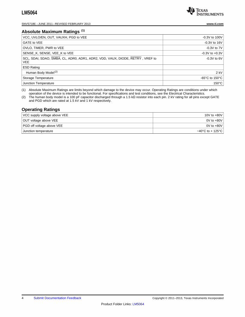
Absolute Maximum Ratings (1)
VCC, UVLO/EN, OUT, VAUXH, PGD to VEE -0.3V to 100V
GATE to VEE -0.3V to 16V
OVLO, TIMER, PWR to VEE -0.3V to 7V
SENSE_K, SENSE, VEE_K to VEE -0.3V to +0.3V
SCL, SDAI, SDAO, SMBA, CL, ADR0, ADR1, ADR2, VDD, VAUX, DIODE, RETRY , VREF to -0.3V to 6VVEE
ESD Rating
Human Body Model (2) 2 kV
Storage Temperature -65°C to 150°C
Junction Temperature 150°C
(1) Absolute Maximum Ratings are limits beyond which damage to the device may occur. Operating Ratings are conditions under whichoperation of the device is intended to be functional. For specifications and test conditions, see the Electrical Characteristics.
(2) The human body model is a 100 pF capacitor discharged through a 1.5 kΩ resistor into each pin. 2 kV rating for all pins except GATEand PGD which are rated at 1.5 kV and 1 kV respectively.
Operating RatingsVCC supply voltage above VEE 10V to +80V
OUT voltage above VEE 0V to +80V
PGD off voltage above VEE 0V to +80V
Junction temperature −40°C to + 125°C
4 Submit Documentation Feedback Copyright © 2011–2013, Texas Instruments Incorporated
Product Folder Links: LM5064
LM5064
www.ti.com SNVS718E –JUNE 2011–REVISED FEBRUARY 2013
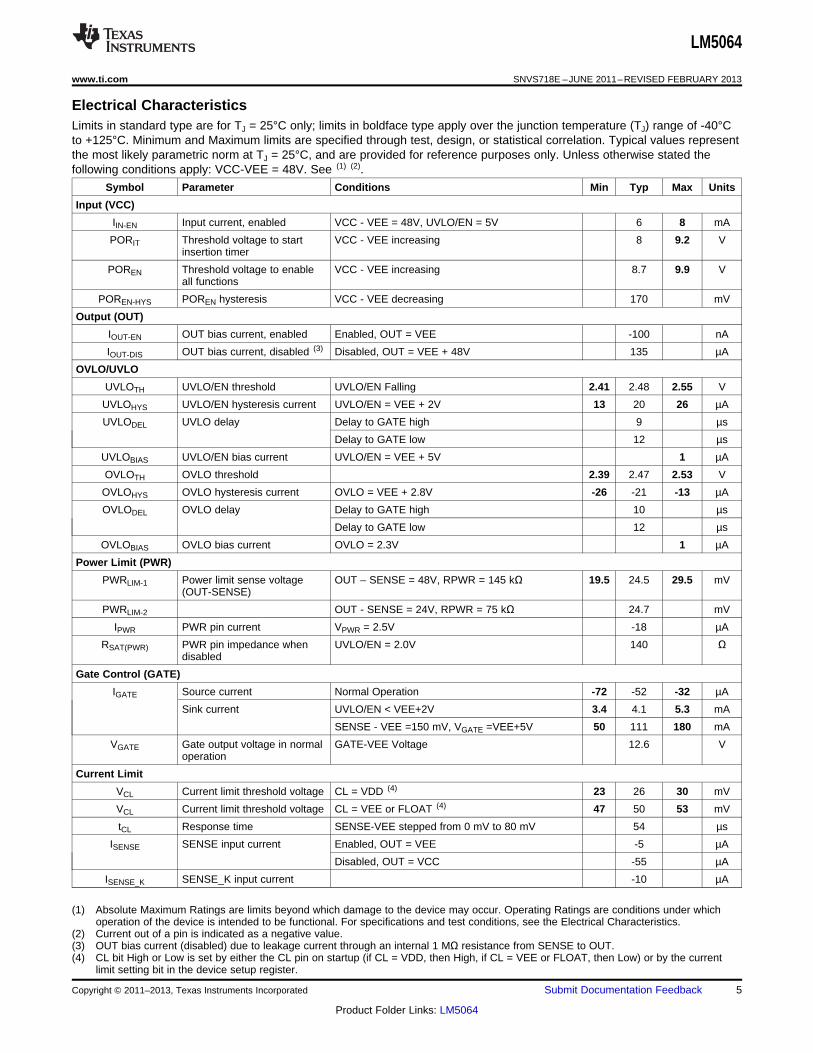
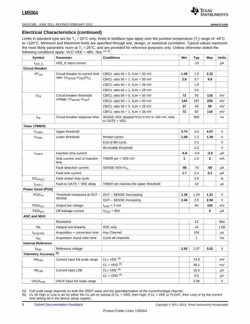
Electrical CharacteristicsLimits in standard type are for TJ = 25°C only; limits in boldface type apply over the junction temperature (TJ) range of -40°Cto +125°C. Minimum and Maximum limits are specified through test, design, or statistical correlation. Typical values representthe most likely parametric norm at TJ = 25°C, and are provided for reference purposes only. Unless otherwise stated thefollowing conditions apply: VCC-VEE = 48V. See (1) (2).
Symbol Parameter Conditions Min Typ Max Units
Input (VCC)
IIN-EN Input current, enabled VCC - VEE = 48V, UVLO/EN = 5V 6 8 mA
PORIT Threshold voltage to start VCC - VEE increasing 8 9.2 Vinsertion timer
POREN Threshold voltage to enable VCC - VEE increasing 8.7 9.9 Vall functions
POREN-HYS POREN hysteresis VCC - VEE decreasing 170 mV
Output (OUT)
IOUT-EN OUT bias current, enabled Enabled, OUT = VEE -100 nA
IOUT-DIS OUT bias current, disabled (3) Disabled, OUT = VEE + 48V 135 µA
OVLO/UVLO
UVLOTH UVLO/EN threshold UVLO/EN Falling 2.41 2.48 2.55 V
UVLOHYS UVLO/EN hysteresis current UVLO/EN = VEE + 2V 13 20 26 µA
UVLODEL UVLO delay Delay to GATE high 9 µs
Delay to GATE low 12 µs
UVLOBIAS UVLO/EN bias current UVLO/EN = VEE + 5V 1 µA
OVLOTH OVLO threshold 2.39 2.47 2.53 V
OVLOHYS OVLO hysteresis current OVLO = VEE + 2.8V -26 -21 -13 µA
OVLODEL OVLO delay Delay to GATE high 10 µs
Delay to GATE low 12 µs
OVLOBIAS OVLO bias current OVLO = 2.3V 1 µA
Power Limit (PWR)
PWRLIM-1 Power limit sense voltage OUT – SENSE = 48V, RPWR = 145 kΩ 19.5 24.5 29.5 mV(OUT-SENSE)
PWRLIM-2 OUT - SENSE = 24V, RPWR = 75 kΩ 24.7 mV
IPWR PWR pin current VPWR = 2.5V -18 µA
RSAT(PWR) PWR pin impedance when UVLO/EN = 2.0V 140 Ωdisabled
Gate Control (GATE)
IGATE Source current Normal Operation -72 -52 -32 µA
Sink current UVLO/EN < VEE+2V 3.4 4.1 5.3 mA
SENSE - VEE =150 mV, VGATE =VEE+5V 50 111 180 mA
VGATE Gate output voltage in normal GATE-VEE Voltage 12.6 Voperation
Current Limit
VCL Current limit threshold voltage CL = VDD (4) 23 26 30 mV
VCL Current limit threshold voltage CL = VEE or FLOAT (4) 47 50 53 mV
tCL Response time SENSE-VEE stepped from 0 mV to 80 mV 54 µs
ISENSE SENSE input current Enabled, OUT = VEE -5 µA
Disabled, OUT = VCC -55 µA
ISENSE_K SENSE_K input current -10 µA
(1) Absolute Maximum Ratings are limits beyond which damage to the device may occur. Operating Ratings are conditions under whichoperation of the device is intended to be functional. For specifications and test conditions, see the Electrical Characteristics.
(2) Current out of a pin is indicated as a negative value.(3) OUT bias current (disabled) due to leakage current through an internal 1 MΩ resistance from SENSE to OUT.(4) CL bit High or Low is set by either the CL pin on startup (if CL = VDD, then High, if CL = VEE or FLOAT, then Low) or by the current
limit setting bit in the device setup register.
Copyright © 2011–2013, Texas Instruments Incorporated Submit Documentation Feedback 5
Product Folder Links: LM5064
LM5064
SNVS718E –JUNE 2011–REVISED FEBRUARY 2013 www.ti.com
Electrical Characteristics (continued)Limits in standard type are for TJ = 25°C only; limits in boldface type apply over the junction temperature (TJ) range of -40°Cto +125°C. Minimum and Maximum limits are specified through test, design, or statistical correlation. Typical values representthe most likely parametric norm at TJ = 25°C, and are provided for reference purposes only. Unless otherwise stated thefollowing conditions apply: VCC-VEE = 48V. See (1) (2).
Symbol Parameter Conditions Min Typ Max Units
IVEE_K VEE_K input current -10 µA
Circuit Breaker
RTCB Circuit breaker to current limit CB/CL ratio bit = 0, ILim = 50 mV 1.45 1.9 2.22ratio: (VSENSE-VVEE)/VCL CB/CL ratio bit = 1, ILim = 50 mV 2.8 3.7 4.9
CB/CL ratio bit = 0, ILim = 26 mV 1.8
CB/CL ratio bit = 1, ILim = 26 mV 3.6
VCB Circuit breaker threshold CB/CL ratio bit = 0, ILim = 50 mV 72 93 116 mVvoltage: (VSENSE-VVEE) CB/CL ratio bit = 1, ILim = 50 mV 144 187 230 mV
CB/CL ratio bit = 0, ILim = 26 mV 37 49 59 mV
CB/CL ratio bit = 1, ILim = 26 mV 72 93 116 mV
tCB Circuit breaker response time SENSE-VEE stepped from 0 mV to 150 mV, time 800 nsto GATE = VEE
Timer (TIMER)
VTMRH Upper threshold 3.74 3.9 4.07 V
VTMRL Lower threshold Restart cycles 1.09 1.2 1.39 V
End of 8th cycle 0.3 V
Re-enable threshold 0.3 V
ITIMER Insertion time current -5.9 -4.8 -3.3 µA
Sink current, end of insertion TIMER pin = VEE+2V 1 1.5 2 mAtime
Fault detection current SENSE-VEE=VCL -95 -74 -50 µA
Fault sink current 1.7 2.4 3.2 µA
DCFAULT Fault restart duty cycle 0.5 %
tFAULT Fault to GATE = VEE delay TIMER pin reaches the upper threshold 15 µs
Power Good (PGD)
PGDTH Threshold measured at OUT - OUT – SENSE Decreasing 1.18 1.24 1.31 VSENSE OUT – SENSE Increasing 2.44 2.5 2.56 V
PGDVOL Output low voltage ISINK = 2 mA 50 150 mV
PGDIOH Off leakage current VPGD = 80V 5 µA
ADC and MUX
Resolution 12 Bits
INL Integral non-linearity ADC only ±4 LSB
tACQUIRE Acquisition + conversion time Any Channel 100 µs
tRR Acquisition round robin time Cycle all channels 1 ms
Internal Reference
VREF Reference voltage 2.93 2.97 3.02 V
Telemetry Accuracy (5)
IINFSR Current input full scale range CL= VEE (6) 74.9 mV
CL = VDD (6) 38.1 mV
IINLSB Current input LSB CL= VEE (6) 18.3 µV
CL = VDD (6) 9.3 µV
VAUXFSR VAUX input full scale range 2.96 V
(5) Full scale range depends on both the VREF value and the gain/attenuation of the current/voltage channel.(6) CL bit High or Low is set by either the CL pin on startup (if CL = VDD, then High, if CL = VEE or FLOAT, then Low) or by the current
limit setting bit in the device setup register.
6 Submit Documentation Feedback Copyright © 2011–2013, Texas Instruments Incorporated
Product Folder Links: LM5064

LM5064
www.ti.com SNVS718E –JUNE 2011–REVISED FEBRUARY 2013
Electrical Characteristics (continued)Limits in standard type are for TJ = 25°C only; limits in boldface type apply over the junction temperature (TJ) range of -40°Cto +125°C. Minimum and Maximum limits are specified through test, design, or statistical correlation. Typical values representthe most likely parametric norm at TJ = 25°C, and are provided for reference purposes only. Unless otherwise stated thefollowing conditions apply: VCC-VEE = 48V. See (1) (2).
Symbol Parameter Conditions Min Typ Max Units
VAUXLSB VAUX input LSB 724 µV
VAUXHFSR VAUXH input full scale range 88.9 V
VAUXHLSB VAUXH input LSB 21.7 mV
OUTLSB OUT pin LSB 21.7 mV
IINACC Input current accuracy SENSE_K-VEE_K = 50 mV, CL = VEE (Note 6) -3.0 3.0 %
VACC VAUX, VAUXH, OUT VAUXH-VEE=48V,OUT - VEE= 48V, VAUX = 2.8V -2.7 2.7 %
PINACC Input power accuracy VCC-VEE = 48V, SENSE_K-VEE_K = 50 mV, CL -4.5 4.5 %= VDD
Diode Temperature Sensor
TACC Temperature accuracy using TA = 25°C to 85°C 2 °Clocal diode
Remote diode resolution 9 bits
IDIODE External diode current source High Level 250 325 µA
Low Level 9.4 µA
Diode current ratio 25.9
VAUX
IIN Input current VAUX = 3V 1 µA
VDD Regulation
VDDOUT VDD regulated output IDD = 0 mA 4.6 4.9 5.15 V
IDD = -10 mA 4.8 V
VDDILIM VDD current limit VDD = 0V -25 -30 -42 mA
VDDPOR VDD voltage reset threshold VDD Rising 4.1 V
PMBus Pin Thresholds (SCL, SDAI/O, SMBA) (7)
VIL Data, clock input low voltage With respect to VEE 0.9 V
VIH Data, clock input high voltage With respect to VEE 2.1 5.5 V
VOL Data output low voltage ISINK = 3 mA 0 0.4 µA
ILEAK Input leakage current SDAI, SMBA, SCL = 5V above VEE 1 µA
Pin Strappable Thresholds (CL, RETRY)
VIH Input high voltage 3 V
ILEAK Input leakage current CL,RETRY = 5V 5 µA
Thermal (8)
θJA Junction to ambient 30 °C/W
θJC Junction to case 4 °C/W
(7) PMBus communication clock rate at final test is 400 kHz.(8) Junction to ambient thermal resistance is highly application and board layout dependent. Specified thermal resistance values for the
package specified is based on a 4-layer, 4"x3", 2/1/1/2 oz. Cu board as per JEDEC standards is used. For detailed information onsoldering plastic HTSSOP packages refer to the Packaging Data Book.
Copyright © 2011–2013, Texas Instruments Incorporated Submit Documentation Feedback 7
Product Folder Links: LM5064

-50 -25 0 25 50 75 100 125-52.2
-52.1
-52.0
-51.9
-51.8
-51.7
-51.6
GA
TE
PIN
SO
UR
CE
CU
RR
EN
T (
A)
TEMPERATURE (°C)-50 -25 0 25 50 75 100 125
5
10
15
20
25
30
VS
NS
VO
LTA
GE
(m
V)
TEMPERATURE (°C)
VCC-VEE=48V, CL = VEE
VCC-VEE=24V, CL = VDD
-50 -25 0 25 50 75 100 125
0
30
60
90
120
150
180
210
240
OU
T P
IN C
UR
RE
NT
(
A)
TEMPERATURE (°C)
VCC = 80V
VCC = 48V
VCC = 9V
-50 -25 0 25 50 75 100 125
6
7
8
9
10
11
12
13
14
15
GA
TE
PIN
VO
LTA
GE
(V
)
TEMPERATURE (°C)
VCC - VEE = 9V
VCC - VEE = 48V
VCC - VEE = 80V
-50 -25 0 25 50 75 100 125-12.0
-11.7
-11.4
-11.1
-10.8
-10.5
-10.2
-9.9
-9.6
-9.3
-9.0
SE
NS
E_K
PIN
CU
RR
EN
T (
A)
TEMPERATURE (°C)-50 -25 0 25 50 75 100 125
-10.6
-10.4
-10.2
-10.0
-9.8
-9.6
-9.4
-9.2
VE
E_K
PIN
CU
RR
EN
T (
A)
TEMPERATURE (°C)
-50 -25 0 25 50 75 100 1255.2
5.4
5.6
5.8
6.0
6.2
6.4V
CC
INP
UT
CU
RR
EN
T (
mA
)
TEMPERATURE (°C)
VCC = 80V
VCC = 48V
VCC = 9V
-50 -25 0 25 50 75 100 125
-5.00
-4.95
-4.90
-4.84
-4.80
-4.75
-4.70
SE
NS
E P
IN C
UR
RE
NT
(
A)
TEMPERATURE (°C)
LM5064
SNVS718E –JUNE 2011–REVISED FEBRUARY 2013 www.ti.com
Typical Performance CharacteristicsUnless otherwise specified the following conditions apply: TJ = 25°C, VCC-VEE = 48V.
VCC Pin Current SENSE Pin Current
SENSE_K Pin Current (Enabled) VEE_K Pin Current (Enabled)
OUT Pin Current (Disabled) GATE Output Voltage (VGATE)
VSNS (SENSE_K-VEE_K) at Power Limit Threshold RPWR =GATE Pin Source Current 75 kΩ
8 Submit Documentation Feedback Copyright © 2011–2013, Texas Instruments Incorporated
Product Folder Links: LM5064

-50 -25 0 25 50 75 100 125
2.962
2.964
2.966
2.968
2.970
2.972
2.974
2.976
VR
EF
(V
)
TEMPERATURE (°C)-50 -25 0 25 50 75 100 125
-1.6
-1.2
-0.8
-0.4
0.0
0.4
0.8
1.2
1.6
IIN E
RR
OR
(%
)
TEMPERATURE (°C)
CL=VEE
-50 -25 0 25 50 75 100 125
20
25
30
35
40
45
50
55
CU
RR
EN
T L
IMIT
TH
RE
SH
OLD
(V
)
TEMPERATURE (°C)
CL = VEE
CL = VDD
-50 -25 0 25 50 75 100 125
40
60
80
100
120
140
160
180
200
CIR
CU
IT B
RE
AK
ER
TH
RE
SH
OLD
(m
V)
TEMPERATURE (°C)
CL = VDD, CB/CL BIT = LOW
CL = VEE, CB/CL BIT = LOW
CL = VEE, CB/CL BIT = HIGH
-50 -25 0 25 50 75 100 125
2.450
2.455
2.460
2.465
2.470
2.475
2.480
OV
LO T
HR
ES
HO
LD (
V)
TEMPERATURE (°C)-50 -25 0 25 50 75 100 125
-20.6
-20.5
-20.4
-20.3
-20.2
-20.1
-20.0
-19.9
OV
LO H
YS
TE
RE
SIS
CU
RR
EN
T (
A)
TEMPERATURE (°C)
-50 -25 0 25 50 75 100 125
2.470
2.472
2.474
2.476
2.478
2.480
2.482
2.484
2.486
2.488
2.490U
VLO
TH
RE
SH
OLD
(V
)
TEMPERATURE (°C)-50 -25 0 25 50 75 100 125
19.2
19.4
19.6
19.8
20.0
20.2
20.4
UV
LO H
YS
TE
RE
SIS
CU
RR
EN
T (
A)
TEMPERATURE (°C)
LM5064
www.ti.com SNVS718E –JUNE 2011–REVISED FEBRUARY 2013
Typical Performance Characteristics (continued)Unless otherwise specified the following conditions apply: TJ = 25°C, VCC-VEE = 48V.
UVLO Threshold UVLO Hysteresis Current
OVLO Threshold OVLO Hysteresis Current
Current Limit Threshold Circuit Breaker Threshold
Reference Voltage IIN Measurement Accuracy (SENSE_K-VEE_K = 50 mV)
Copyright © 2011–2013, Texas Instruments Incorporated Submit Documentation Feedback 9
Product Folder Links: LM5064

VGATE (20V/Div)
VOUT (25V/Div)
VSYS (25V/Div)
VPGOOD (2V/Div)
VOUT (25V/Div)
VSYS (25V/Div)
VTIMER (2V/Div)
VOUT (20V/Div)
VSYS (20V/Div) (-48V)
VGATE (20V/Div)
VTIMER (2V/Div)
VOUT (20V/Div)
VSYS (5V/Div)
IIN (5A/Div)
VTIMER (2V/Div)
VOUT (20V/Div)
VSYS (20V/Div)
IIN (5A/Div)
INSERTION DELAY = 140 ms
-50 -25 0 25 50 75 100 125
-1.0
-0.8
-0.6
-0.4
-0.2
0.0
0.2
0.4
0.6
0.8
1.0P
IN E
RR
OR
(%
)
TEMPERATURE (°C)
CL=VEE
LM5064
SNVS718E –JUNE 2011–REVISED FEBRUARY 2013 www.ti.com
Typical Performance Characteristics (continued)Unless otherwise specified the following conditions apply: TJ = 25°C, VCC-VEE = 48V.
PIN Measurement Accuracy (SENSE_K-VEE_K = 50 mV) Startup (Insertion Delay)
40 ms/divShort Circuit VOUT Startup (1A Load)
40 ms/div1s/divStartup (UVLO/EN, OVLO) Startup (PGD)
400 ms/div400 ms/div
10 Submit Documentation Feedback Copyright © 2011–2013, Texas Instruments Incorporated
Product Folder Links: LM5064

VTIMER (2V/Div)
VOUT (20V/Div) (-48V)
VIN (20V/Div)
IIN (1A/Div)
VTIMER (2V/Div)
VOUT (20V/Div) (-48V)
VGATE (10V/Div)
VTIMER (2V/Div)
VOUT (20V/Div)
VGATE (5V/Div)
IIN (5A/Div)
VTIMER (2V/Div)
VOUT (20V/Div)
VGATE (5V/Div)
IIN (5A/Div)
CL = 8.7A CB=1.8 x CL
LM5064
www.ti.com SNVS718E –JUNE 2011–REVISED FEBRUARY 2013
Typical Performance Characteristics (continued)Unless otherwise specified the following conditions apply: TJ = 25°C, VCC-VEE = 48V.
Current Limit Event (CL = VDD) Circuit Breaker Event (CL = VDD)
400 µs/div
4 ms/divRetry Event (RETRY = VEE) Latch Off (RETRY = VDD)
400 ms/div 100 ms/div
Copyright © 2011–2013, Texas Instruments Incorporated Submit Documentation Feedback 11
Product Folder Links: LM5064

VEE
GATE
74 µA
Fault Timer
TIMER
Current Limit Threshold
Power Limit Threshold
4.1 mA
Current Limit/Power LimitControl
111mA
1/30
VAUX
DIODE
SCL
SDAO
SMBA
DiodeTempSense
VDD
12 bitADC
OV
UV
UVOV
Current Telemetry Sense
1 M:
Circuit BreakerThreshold
SDAI
Ref
VREF
VEE
VCCLM5064
VEE
VEE
VEE
VEE
1.24V/2.5V
TIME AND GATE LOGIC CONTROL
GATECONTROL
1.5 mA End
InsertionTime Fault
Discharge
Insertion TimerPOR
EnablePOR
3.9V
1.2V
0.3V
2.47V
2.48V
8.7V/8.53VVCC
8VVCC
21 µA
18 µA
26/50 mV
CL
ADR0
ADR1
ADR2
MEASUREMENT/FAULT REGISTERS
SMBUSINTERFACE
ADDRESSDECODER
TELEMETRYSTATE
MACHINE
AM
UX S
/H 1/30
VDDREG
(26|50) x (1.8,3.6|1.9,3.7) mV
IDS
VDS
PW
R
OV
LO
UV
LO /EN
RE
TR
Y2.4 µA
52 µA
4.8 µA
Insertion Timer
VEE
12.6V
VCC
20 µA
SE
NS
E
OU
T
VE
E_K
PG
D
VA
UX
H
SE
NS
E_K
LM5064
SNVS718E –JUNE 2011–REVISED FEBRUARY 2013 www.ti.com
BLOCK DIAGRAM
Figure 1. Block Diagram
12 Submit Documentation Feedback Copyright © 2011–2013, Texas Instruments Incorporated
Product Folder Links: LM5064
LM5064
www.ti.com SNVS718E –JUNE 2011–REVISED FEBRUARY 2013
FUNCTIONAL DESCRIPTION
The LM5064 is designed to control the in-rush current to the load upon insertion of a circuit card into a livebackplane or other “hot” power source, thereby limiting the voltage sag on the backplane’s supply and the dv/dtof the voltage applied to the load. The effect from the insertion event on other circuits in the system is minimized,preventing possible unintended resets. A controlled shutdown when the circuit card is removed can also beimplemented using the LM5064.
In addition to a programmable current limit, the LM5064 monitors and limits the maximum power dissipation inthe series pass device (Q1) to maintain operation within the device’s Safe Operating Area (SOA). Either currentlimiting or power limiting for an extended period of time (user defined) results in the shutdown of the series passdevice. In this event, the LM5064 can latch off or repetitively retry based on the hardware setting of the RETRYpin. Once started, the number of retries can be set to 0, 1, 2, 4, 8, 16, or infinite. The circuit breaker functionquickly switches off the series pass device upon detection of a severe over-current condition. Programmableunder-voltage lockout (UVLO) and over-voltage lockout (OVLO) circuits shut down the LM5064 when the systeminput voltage (VSYS) is outside the desired operating range.
The telemetry capability of the LM5064 provides intelligent monitoring of the input voltage, output voltage, inputcurrent, input power, temperature, and an auxiliary input. The LM5064 also provides a peak capture of the inputpower and programmable hardware averaging of the input voltage, current, power, and output voltage. Warningthresholds which trigger the SMBA pin may be programmed for input and output voltage, current, power andtemperature via the PMBus interface. Additionally, the LM5064 is capable of detecting damage to the externalMOSFET, Q1.
Operating Voltage
The LM5064 operating voltage is the voltage supplied between VCC and VEE (VCC-VEE) which has anoperating range of 10V to 80V with a 100V transient capability. All signals to the IC are referenced to the VEEvoltage which acts as the effective return path for the IC.
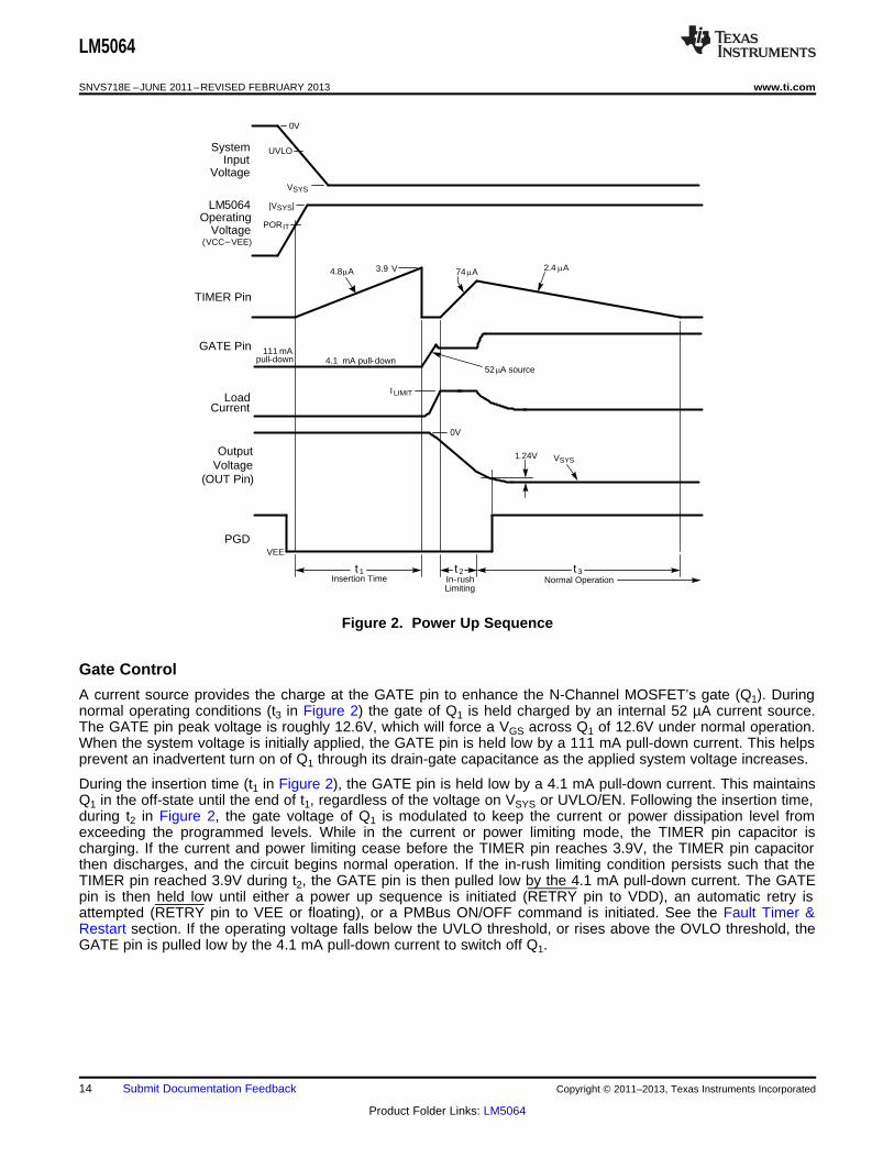
Power Up Sequence
Referring to Figure 2, as the system voltage (VSYS) initially increases, the external N-channel MOSFET (Q1) isheld off by an internal 111 mA pull-down current at the GATE pin. The strong pull-down current at the GATE pinprevents an inadvertent turn on as the MOSFET’s gate-to-drain (Miller) capacitance is charged. Additionally, theTIMER pin is initially held at VEE. When the operating voltage of the LM5064 (VCC - VEE) reaches the PORITthreshold, the insertion time begins. During the insertion time, the capacitor at the TIMER pin (CT) is charged bya 4.8 µA current source, and Q1 is held off by a 4.1 mA pull-down current at the GATE pin regardless of the inputvoltage. The insertion time delay allows ringing and transients on VSYS to settle before Q1 is enabled. Theinsertion time ends when the TIMER pin voltage reaches 3.9V. CT is then quickly discharged by an internal 1.5mA pull-down current. The GATE pin then switches on Q1 when the operating voltage exceeds the UVLOthreshold. If the operating voltage is above the UVLO threshold at the end of the insertion time,(t1 in Figure 2) theGATE pin sources 52 µA to charge the gate capacitance of Q1. The maximum voltage on GATE is limited by aninternal 12.6V zener diode to VEE.
As the voltage at the OUT pin transitions to VSYS, the LM5064 monitors the drain current and power dissipation ofMOSFET Q1. In-rush current limiting and/or power limiting circuits actively control the current delivered to theload. During the in-rush limiting interval (t2 in Figure 2), an internal 74 µA fault timer current source charges CT. IfQ1’s power dissipation and the input current reduce below their respective limiting thresholds before the TIMERpin reaches 3.9V, the 74 µA current source is switched off, and CT is discharged by the internal 2.4 µA currentsink (t3 in Figure 2). The in-rush limiting will no longer engage unless a current-limit condition occurs.
If the TIMER pin voltage reaches 3.9V before in-rush current limiting or power limiting ceases during t2, a fault isdeclared and Q1 is turned off. See the Fault Timer & Restart section for a complete description of the fault mode.
The LM5064 will assert the SMBA pin after the operating voltage has exceeded the POR threshold to indicatethat the volatile memory and device settings are in their default state. The CONFIG_PRESET bit within theMFR_SPECIFIC_17 register (E1h) indicates default configuration of warning thresholds and device operation andwill remain high until a CLEAR_FAULTS command is received.
Copyright © 2011–2013, Texas Instruments Incorporated Submit Documentation Feedback 13
Product Folder Links: LM5064
TIMER Pin
Load Current
PGD
UVLO
LimitingNormal Operation
GATE Pin
Insertion Time
Operating Voltage
Output Voltage
VEE
2.4 PA74PA
52PA source
3.9 V
0V
4.1 mA pull-down
4.8 PA
1.24V
ILIMIT
VSYS
pull-down111 mA
0V
VSYS
PORIT
System Input
Voltage
(VCC± VEE)
LM5064
(OUT Pin)
t 3t 2In-rush
t 1
|VSYS|
LM5064
SNVS718E –JUNE 2011–REVISED FEBRUARY 2013 www.ti.com
Figure 2. Power Up Sequence
Gate Control
A current source provides the charge at the GATE pin to enhance the N-Channel MOSFET’s gate (Q1). Duringnormal operating conditions (t3 in Figure 2) the gate of Q1 is held charged by an internal 52 µA current source.The GATE pin peak voltage is roughly 12.6V, which will force a VGS across Q1 of 12.6V under normal operation.When the system voltage is initially applied, the GATE pin is held low by a 111 mA pull-down current. This helpsprevent an inadvertent turn on of Q1 through its drain-gate capacitance as the applied system voltage increases.
During the insertion time (t1 in Figure 2), the GATE pin is held low by a 4.1 mA pull-down current. This maintainsQ1 in the off-state until the end of t1, regardless of the voltage on VSYS or UVLO/EN. Following the insertion time,during t2 in Figure 2, the gate voltage of Q1 is modulated to keep the current or power dissipation level fromexceeding the programmed levels. While in the current or power limiting mode, the TIMER pin capacitor ischarging. If the current and power limiting cease before the TIMER pin reaches 3.9V, the TIMER pin capacitorthen discharges, and the circuit begins normal operation. If the in-rush limiting condition persists such that theTIMER pin reached 3.9V during t2, the GATE pin is then pulled low by the 4.1 mA pull-down current. The GATEpin is then held low until either a power up sequence is initiated (RETRY pin to VDD), an automatic retry isattempted (RETRY pin to VEE or floating), or a PMBus ON/OFF command is initiated. See the Fault Timer &Restart section. If the operating voltage falls below the UVLO threshold, or rises above the OVLO threshold, theGATE pin is pulled low by the 4.1 mA pull-down current to switch off Q1.
14 Submit Documentation Feedback Copyright © 2011–2013, Texas Instruments Incorporated
Product Folder Links: LM5064

LM5064
www.ti.com SNVS718E –JUNE 2011–REVISED FEBRUARY 2013
Current Limit
The current limit threshold is reached when the voltage across the sense resistor RS (SENSE to VEE) exceedsthe internal voltage limit of 26 mV or 50 mV depending on whether the CL pin is connected to VDD or VEE,respectively. In the current limiting condition, the GATE voltage is controlled to limit the current in MOSFET Q1.While the current limit circuit is active, the fault timer is active as described in the Fault Timer & Restart section. Ifthe load current falls below the current limit threshold before the end of the Fault Timeout Period, the LM5064resumes normal operation. If the current limit condition persists for longer than the Fault Timeout Period set byCT, the IIN OC Fault bit in the STATUS_INPUT (7Ch) register, the INPUT bit in the STATUS_WORD (79h)register, and IIN_OC/PFET_OP_FAULT bit in the DIAGNOSTIC_WORD (E1h) register will be toggled high andSMBA pin will be asserted. SMBA toggling can be disabled using the ALERT_MASK (D8h) register. For properoperation, the RS resistor value should be no higher than 200 mΩ. Higher values may create instability in thecurrent limit control loop. The current limit threshold pin value may be overridden by setting appropriate bits inthe DEVICE_SETUP register (D9h).
Circuit Breaker
If the load current increases rapidly (e.g., the load is short circuited), the current in the sense resistor (RS) mayexceed the current limit threshold before the current limit control loop is able to respond. If the current exceeds1.9x or 3.7x (CL = VEE) the current limit threshold, Q1 is quickly switched off by the 111 mA pull-down current atthe GATE pin, and a Fault Timeout Period begins. When the voltage across RS falls below the circuit breaker(CB) threshold, the 111 mA pull-down current at the GATE pin is switched off, and the gate voltage of Q1 is thendetermined by the current limit or the power limit functions. If the TIMER pin reaches 3.9V before the currentlimiting or power limiting condition ceases, Q1 is switched off by the 4.1 mA pull-down current at the GATE pin asdescribed in the Fault Timer & Restart section. A circuit breaker event will cause theCIRCUIT_BREAKER_FAULT bit in the STATUS_MFR_SPECIFIC (80h) and DIAGNOSTIC_WORD (E1h)registers to be toggled high, and SMBA pin will be asserted unless this feature is disabled using theALERT_MASK (D8h) register. The circuit breaker pin configuration may be overridden by setting appropriate bitsin the DEVICE_SETUP (D9h) register.
Power Limit
An important feature of the LM5064 is the MOSFET power limiting. The power limit function can be used tomaintain the maximum power dissipation of MOSFET Q1 within the device SOA rating. The LM5064 determinesthe power dissipation in Q1 by monitoring its drain-source voltage (OUT to SENSE), and the drain currentthrough the RS (SENSE to VEE). The product of the current and voltage is compared to the power limit thresholdprogrammed by the resistor at the PWR pin. If the power dissipation reaches the limiting threshold, the GATEvoltage is modulated to regulate the current in Q1. While the power limiting circuit is active, the fault timer isactive as described in the Fault Timer & Restart section. If the power limit condition persists for longer than theFault Timeout Period set by the timer capacitor, CT, the IIN OC Fault bit in the STATUS_INPUT (7Ch) register,the INPUT bit in the STATUS_WORD (79h) register, and the IIN_OC/PFET_OP_FAULT bit in theDIAGNOSTIC_WORD (E1h) register will be toggled high and SMBA pin will be asserted unless this feature isdisabled using the ALERT_MASK (D8h) register.
Fault Timer & Restart
When the current limit or power limit threshold is reached during turn-on, or as a result of a fault condition, thegate-to-source voltage of Q1 is modulated to regulate the load current and power dissipation in Q1. When eitherlimiting function is active, a 74 µA fault timer current source charges the external capacitor (CT) at the TIMER pinas shown in Figure 2(Fault Timeout Period). If the fault condition subsides during the Fault Timeout Period beforethe TIMER pin reaches 3.9V, the LM5064 returns to the normal operating mode and CT is discharged by the 1.5mA current sink. If the TIMER pin reaches 3.9V during the Fault Timeout Period, Q1 is switched off by a 4.1 mApull-down current at the GATE pin. The subsequent restart procedure then depends on the selected retryconfiguration.
If the RETRY pin is high (VDD), the LM5064 latches the GATE pin low at the end of the Fault Timeout Period. CTis then discharged to VEE by the 2.4 µA fault current sink. The GATE pin is held low by the 4.1 mA pull-downcurrent until a power up sequence is externally initiated by cycling the operating voltage (VCC-VEE), ormomentarily pulling the UVLO/EN pin below its threshold with an open-collector or open-drain device as shownin Figure 3. The voltage at the TIMER pin must be <0.3V for the restart procedure to be effective. TheTIMER_LATCHED_OFF bit in the DIAGNOSTIC_WORD (E1h) register will remain high while the latched offcondition persists.
Copyright © 2011–2013, Texas Instruments Incorporated Submit Documentation Feedback 15
Product Folder Links: LM5064

LoadCurrent
GATEPin
TIMERPin
3.9V
1.2V1 2 3 7 8
4.1 mApulldown
52 PAGate Charge
74 PA
2.4 PA
Fault TimeoutPeriod
0.3V
FaultDetection ILIMIT
tRESTART
LM5064
LatchControl
VCC
UVLO/EN
OVLO
VEE
R1
R2
R3
VSYS
LM5064
SNVS718E –JUNE 2011–REVISED FEBRUARY 2013 www.ti.com
Figure 3. Latched Fault Restart Control
The LM5064 provides an automatic restart sequence which consists of the TIMER pin cycling between 3.9V and1.2V eight times after the Fault Timeout Period, as shown in Figure 4. The period of each cycle is determined bythe 74 µA charging current, and the 2.4 µA discharge current, and the value of the capacitor CT. When theTIMER pin reaches 0.3V during the eighth high-to-low ramp, the 52 µA current source at the GATE pin turns onQ1. If the fault condition is still present, the Fault Timeout Period and the restart sequence repeat. The RETRYpin allows selecting no retries or infinite retries. Finer control of the retry behavior can be achieved through theDEVICE_SETUP (D9h) register. Retry counts of 0, 1, 2, 4, 8, 16 or infinite may be selected by setting theappropriate bits in the DEVICE_SETUP (D9h) register.
Figure 4. Restart Sequence
Under-Voltage Lockout (UVLO)
The series pass MOSFET (Q1) is enabled when the input supply voltage (VSYS) is within the operating rangedefined by the programmable under-voltage lockout (UVLO) and over-voltage lockout (OVLO) levels. Typically,the UVLO level at VSYS is set with a resistor divider (R1-R3) as shown in Figure 5. Referring to the BlockDiagram when VSYS is below the UVLO level, the internal 20 µA current source at UVLO/EN is enabled, thecurrent source at OVLO is off, and Q1 is held off by the 4.1 mA pull-down current at the GATE pin. As VSYS isincreased, raising the voltage at UVLO/EN above its threshold with respect to VEE, the 20 µA current source atUVLO/EN is switched off, increasing the voltage at UVLO/EN, providing hysteresis for this threshold. With theUVLO/EN pin above its threshold, Q1 is switched on by the 52 µA current source at the GATE pin if the insertiontime delay has expired.
See the Application Information section for a procedure to calculate the values of the threshold setting resistors(R1-R3). The minimum possible UVLO level at VSYS can be set by connecting the UVLO/EN pin to VCC. In thiscase Q1 is enabled after the insertion time when the operating voltage (VCC-VEE) reaches the POR threshold.After power up an UVLO condition will cause the INPUT bit in the STATUS_WORD (79h) register, theVIN_UV_FAULT bit in the STATUS_INPUT (7Ch) register, and the VIN_UNDERVOLTAGE_FAULT bit in theDIAGNOSTIC_WORD (E1h) registers to be toggled high and SMBA pin will be pulled low unless this feature isdisabled using the ALERT_MASK (D8h) register.
16 Submit Documentation Feedback Copyright © 2011–2013, Texas Instruments Incorporated
Product Folder Links: LM5064

LM5064ShutdownControl
VCC
UVLO
OVLO
VEE
R1
R2
R3
VSYS
LM5064
www.ti.com SNVS718E –JUNE 2011–REVISED FEBRUARY 2013
Over-Voltage Lockout (OVLO)
The series pass MOSFET (Q1) is enabled when the input supply voltage (VSYS) is within the operating rangedefined by the programmable under-voltage lockout (UVLO) and over-voltage lockout (OVLO) levels. If VSYSraises the OVLO pin voltage above its threshold (2.47V above VEE), Q1 is switched off by the 4.1 mA pull-downcurrent at the GATE pin, denying power to the load. When the OVLO pin is above its threshold, the internal 21µA current source at OVLO is switched on, raising the voltage at OVLO to provide threshold hysteresis. WhenVSYS is reduced below the OVLO level Q1 is re-enabled. An OVLO condition will toggle the VIN_OV_FAULT bit inthe STATUS_INPUT (7Ch) register, the INPUT bit in the STATUS_WORD (79h) register and theVIN_OVERVOLTAGE_FAULT bit in the DIAGNOSTIC_WORD (E1h) register. The SMBA pin will be pulled lowunless this feature is disabled using the ALERT_MASK (D8h) register.
Shutdown Control
The load current can be remotely switched off by taking the UVLO/EN pin below its threshold with an opencollector or open drain device, as shown in Figure 5. Upon releasing the UVLO/EN pin the LM5064 switches onthe load current with in-rush current and power limiting.
Figure 5. Shutdown Control
Power Good Pin
The Power Good output indicator pin (PGD) is connected to the drain of an internal N-channel MOSFET. Anexternal pull-up resistor is required at PGD to an appropriate voltage to indicate the status to downstreamcircuitry. The off-state voltage at the PGD pin must be more positive than VEE, and can be up to 80V above VEEwith transient capability to 100V. PGD is switched high at the end of the turn-on sequence when the voltage fromOUT to SENSE (the external MOSFET’s VDS) decreases below 1.24V. PGD switches low if the MOSFET’s VDSincreases passed 2.5V, if the system input voltage goes below the UVLO threshold or above the OVLOthreshold, or if a fault is detected. However, the PGD output cannot stay low when the operating voltage (VCC-VEE) is less than 2V.
VDD Sub-Regulator
The LM5064 contains an internal linear sub-regulator which steps down the VCC voltage to generate a 4.9V rail(above VEE) used for powering low voltage circuitry. The VDD sub-regulator should be used as the pull-upsupply for the CL, RETRY, ADR2, ADR1, ADR0 pins if they are to be tied high. It may also be used as the pull-up supply for the PGD and the SMBus signals (SDA, SCL, SMBA). The VDD sub-regulator is not designed todrive high currents. Careful consideration of internal power dissipation should be practiced when VDD is loadedwith other integrated circuits. The VDD pin is current limited to 30 mA in order to protect the LM5064 in the eventof a short. The sub-regulator requires a ceramic bypass capacitance (terminated to VEE) having a value of 1 µFor greater to be placed as close to the VDD pin as the PCB layout allows.
Copyright © 2011–2013, Texas Instruments Incorporated Submit Documentation Feedback 17
Product Folder Links: LM5064

LM5064
SNVS718E –JUNE 2011–REVISED FEBRUARY 2013 www.ti.com
Remote Temperature Sensing
The LM5064 is designed to measure temperature remotely using an MMBT3904 NPN transistor. The base andcollector of the MMBT3904 should be connected to the DIODE pin and the emitter to VEE. Place the MMBT3904near the device that requires temperature sensing. If the temperature of the hot swap pass MOSFET, Q1, is to bemeasured, the MMBT3904 should be placed as close to Q1 as the layout allows. The temperature is measuredby means of a change in the diode voltage in response to a step in current supplied by the DIODE pin. TheDIODE pin sources a constant 9.4 µA but pulses 250 µA once every millisecond in order to measure the diodetemperature. Care must be taken in the PCB layout to keep the parasitic resistance between the DIODE pin andthe MMBT3904 low so as not to degrade the measurement. Additionally, a small 1000 pF bypass capacitorshould be placed in parallel with the MMBT3904 (collector to emitter) to reduce the effects of noise. Thetemperature can be read using the READ_TEMPERATURE_1 PMBus command (8Dh). The default limits of theLM5064 will cause SMBA pin to be pulled low if the measured temperature exceeds 125°C and will disable Q1 ifthe temperature exceeds 150°C. These thresholds can be reprogrammed via the PMBus interface using theOT_WARN_LIMIT (51h) and OT_FAULT_LIMIT (4Fh) commands. If the temperature measurement andprotection capability of the LM5064 are not used, the DIODE pin should be connected to VEE.
Erroneous temperature measurements may result when the device input voltage is below the minimum operatingvoltage (10V) due to VREF dropping out below the nominal voltage (2.97V). At higher ambient temperatures, thismeasurement could read a value higher than the OT_FAULT_LIMIT, and will trigger a fault, disabling Q1. In thiscase, the faults should be removed and the device reset by writing a 0h, followed by an 80h to the OPERATION(01h) register.
Damaged MOSFET Detection
The LM5064 is able to detect whether the external MOSFET, Q1, is damaged under certain conditions. If thevoltage across the sense resistor exceeds 4 mV while the GATE voltage is low or the internal logic indicates thatthe GATE should be low, the EXT_MOSFET_SHORTED bit in the STATUS_MFR_SPECIFIC (80h) andDIAGNOSTIC_WORD (E1h) registers will be toggled high and the SMBA pin will be asserted unless this featureis disabled using the ALERT_MASK register (D8h). This method effectively determines whether Q1 is shortedbecause of damage present between the drain and gate and/or drain and source.
Enabling/Disabling and Resetting
The output can be disabled at any time during normal operation by either pulling the UVLO/EN pin to below itsthreshold or the OVLO pin above its threshold, causing the GATE voltage to be forced low with a pull-downstrength of 4.1 mA. Toggling the UVLO/EN pin will also reset the LM5064 from a latched-off state due to an over-current or over-power limit condition which has caused the maximum allowed number of retries to be exceeded.While the UVLO/EN or OVLO pins can be used to disable the output they have no effect on the volatile memoryor address location of the LM5064. User stored values for address, device operation, and warning and faultlevels programmed via the SMBus are preserved while the LM5064 is powered regardless of the state of theUVLO/EN and OVLO pins.The output may also be enabled or disabled by writing 80h or 0h to the OPERATION(01h) register. To re-enable after a fault, the fault condition should be cleared and the OPERATION (01h) registershould be written with a 0h and then 80h.
The SMBus address of the LM5064 is captured based on the states (VEE, NC, VDD) of the ADR0, ADR1, andADR2 pins during turn-on and is latched into a volatile register once VDD has exceeded its POR threshold of4.1V. Reassigning or postponing the address capture is accomplished by holding the VREF pin to VEE. Pullingthe VREF pin low will also reset the logic and erase the volatile memory of the LM5064. Once released, theVREF pin will charge up to its final value and the address will be latched into a volatile register once the voltageat the VREF exceeds 2.55V.
18 Submit Documentation Feedback Copyright © 2011–2013, Texas Instruments Incorporated
Product Folder Links: LM5064
UVLO/EN
SCL
PWR
VEE_K
TIMER
PGD
GATE
SDAO
SMBA
ADR0ADR1ADR2
VAUX
VDD
OVLO
CL
DIODE
SDAI
VCC
OUT
RETRY
VREFVEE
SENSE
SENSE_ K
VAUXH
OUTPUT
GND
VSYS
VDD
LM5064
LOAD
EN
R1
R3
R2
CT1 µF 1 µF
RPWRRS
RPG
Q1
GND
+
COUT
Z1
QT
D1
200 k:
8.87 k:
7.87 k:5.0SMDJ60A
3 m:
MMBT3904 FDB047N10
30.1 k:
B380-13-F
0.15 µF
100 k:
200 µF
LM5064
www.ti.com SNVS718E –JUNE 2011–REVISED FEBRUARY 2013
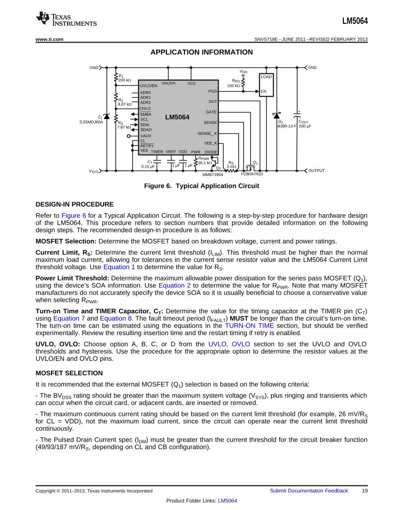
APPLICATION INFORMATION
Figure 6. Typical Application Circuit
DESIGN-IN PROCEDURE
Refer to Figure 6 for a Typical Application Circuit. The following is a step-by-step procedure for hardware designof the LM5064. This procedure refers to section numbers that provide detailed information on the followingdesign steps. The recommended design-in procedure is as follows:
MOSFET Selection: Determine the MOSFET based on breakdown voltage, current and power ratings.
Current Limit, RS: Determine the current limit threshold (ILIM). This threshold must be higher than the normalmaximum load current, allowing for tolerances in the current sense resistor value and the LM5064 Current Limitthreshold voltage. Use Equation 1 to determine the value for RS.
Power Limit Threshold: Determine the maximum allowable power dissipation for the series pass MOSFET (Q1),using the device’s SOA information. Use Equation 2 to determine the value for RPWR. Note that many MOSFETmanufacturers do not accurately specify the device SOA so it is usually beneficial to choose a conservative valuewhen selecting RPWR.
Turn-on Time and TIMER Capacitor, CT: Determine the value for the timing capacitor at the TIMER pin (CT)using Equation 7 and Equation 8. The fault timeout period (tFAULT) MUST be longer than the circuit’s turn-on time.The turn-on time can be estimated using the equations in the TURN-ON TIME section, but should be verifiedexperimentally. Review the resulting insertion time and the restart timing if retry is enabled.
UVLO, OVLO: Choose option A, B, C, or D from the UVLO, OVLO section to set the UVLO and OVLOthresholds and hysteresis. Use the procedure for the appropriate option to determine the resistor values at theUVLO/EN and OVLO pins.
MOSFET SELECTION
It is recommended that the external MOSFET (Q1) selection is based on the following criteria:
- The BVDSS rating should be greater than the maximum system voltage (VSYS), plus ringing and transients whichcan occur when the circuit card, or adjacent cards, are inserted or removed.
- The maximum continuous current rating should be based on the current limit threshold (for example, 26 mV/RSfor CL = VDD), not the maximum load current, since the circuit can operate near the current limit thresholdcontinuously.
- The Pulsed Drain Current spec (IDM) must be greater than the current threshold for the circuit breaker function(49/93/187 mV/RS, depending on CL and CB configuration).
Copyright © 2011–2013, Texas Instruments Incorporated Submit Documentation Feedback 19
Product Folder Links: LM5064
72026)(7¶6
SOURCE
HIGH CURRENT PATH
SENSE RESISTOR
FROM SYSTEM
INPUT VOLTAGE SR
6232220
VE
E_K
SE
NS
E_K
LM
5064
21
SE
NS
E
VE
E20
LM5064
SNVS718E –JUNE 2011–REVISED FEBRUARY 2013 www.ti.com
- The SOA (Safe Operating Area) chart of the device, and the thermal properties, should be used to determinethe maximum power dissipation threshold set by the RPWR resistor. The programmed maximum power dissipationshould have a reasonable margin from the maximum power defined by the MOSFET’s SOA curve. If the deviceis set to infinitely retry, the MOSFET will be repeatedly stressed during fault restart cycles. The MOSFETmanufacturer should be consulted for guidelines.
- RDS(on) should be sufficiently low such that the power dissipation at maximum load current (ILIM2 x RDS(on)) does
not raise its junction temperature above the manufacturer’s recommendation.
- The gate-to-source voltage provided by the LM5064 can be as high as 12.6V. Q1 must be able to tolerate thisvoltage for its VGS rating. An additional zener diode can be added from GATE to VEE to lower this voltage andlimit the peak VGS.
CURRENT LIMIT (RS)
The LM5064 monitors the current in the external MOSFET Q1 by measuring the voltage across the senseresistor (RS), connected from SENSE to VEE. The required resistor value is calculated from:
(1)
where ILIM is the desired current limit threshold. If the voltage across RS reaches VCL, the current limit circuitmodulates the gate of Q1 to regulate the current at ILIM. While the current limiting circuit is active, the fault timer isactive as described in the Fault Timer & Restart section. For proper operation, RS must be less than 200 mΩ.
VCL can be set to either 26 mV or 50 mV via hardware and/or software. This setting defaults to use of CL pinwhich, when connected to VDD is 26 mV, or VEE is 50 mV. The value, when powered, can be set via the PMBuswith the DEVICE_SETUP (D9h) command, which defaults to the 26 mV setting.
Once the desired setting is known, calculate the shunt based on that input voltage and maximum current. Whilethe maximum load current in normal operation can be used to determine the required power rating for resistorRS, basing it on the current limit value provides a more reliable design since the circuit can operate near thecurrent limit threshold continuously. The resistor’s surge capability must also be considered since the circuitbreaker threshold is 1.9 or 3.7 times the current limit threshold.
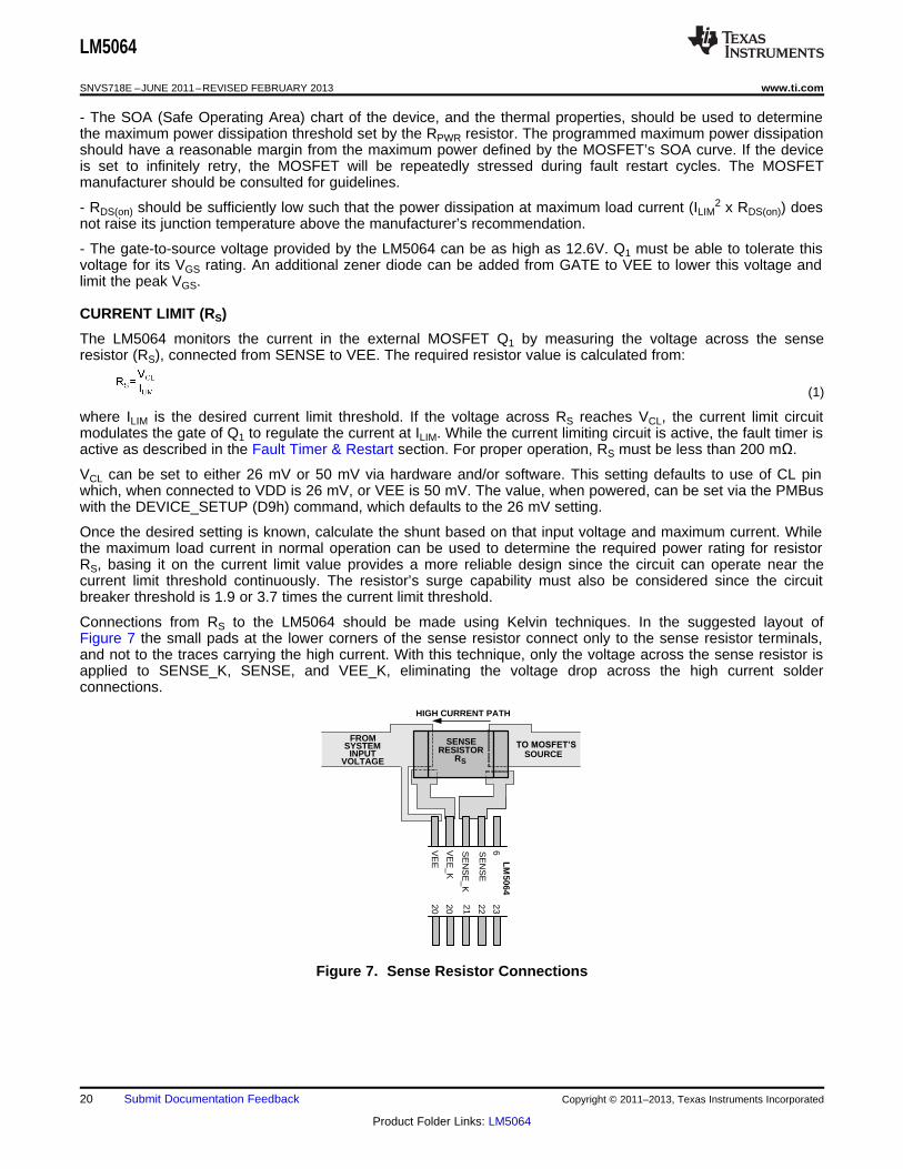
Connections from RS to the LM5064 should be made using Kelvin techniques. In the suggested layout ofFigure 7 the small pads at the lower corners of the sense resistor connect only to the sense resistor terminals,and not to the traces carrying the high current. With this technique, only the voltage across the sense resistor isapplied to SENSE_K, SENSE, and VEE_K, eliminating the voltage drop across the high current solderconnections.
Figure 7. Sense Resistor Connections
20 Submit Documentation Feedback Copyright © 2011–2013, Texas Instruments Incorporated
Product Folder Links: LM5064

LM5064
www.ti.com SNVS718E –JUNE 2011–REVISED FEBRUARY 2013
POWER LIMIT THRESHOLD
The LM5064 determines the power dissipation in the external MOSFET (Q1) by monitoring the drain current (thecurrent in RS) and the VDS of Q1 (OUT to SENSE pins). The resistor at the PWR pin (RPWR) sets the maximumpower dissipation for Q1, and is calculated from the following equation:
(2)
where PMOSFET(LIM) is the desired power limit threshold for Q1, and RS is the current sense resistor described inthe CURRENT LIMIT (RS) section. For example, if RS is 3 mΩ, VIN = 48V, and the desired power limit thresholdis 80W, RPWR calculates to 30.1 kΩ (standard 1% value). If Q1’s power dissipation reaches the threshold Q1’sgate is modulated to regulate the load current, keeping Q1’s power from exceeding the threshold. For properoperation of the power limiting feature, RPWR must be ≤150 kΩ. While the power limiting circuit is active, the faulttimer is active as described in the Fault Timer & Restart section. Typically, power limit is reached during startup,or if the output voltage falls due to a severe over-load or short circuit. The programmed maximum powerdissipation should have a reasonable margin from the maximum power defined by the SOA chart, especially ifretry is enabled, because the MOSFET will be repeatedly stressed during fault restart cycles. The MOSFETmanufacturer should be consulted for guidelines. If the application does not require use of the power limitfunction the PWR pin can be left open. The accuracy of the power limit function at turn-on may degrade if a verylow power dissipation limit is set. The reason for this caution is that the voltage across the sense resistor, whichis monitored and regulated by the power limit circuit, is lowest at turn-on when the regulated current is at aminimum. The voltage across the sense resistor during power limit can be expressed as follows:
(3)
where ILIM is the current in RS, and VDS is the voltage across Q1. For example, if the power limit is set at 80Wwith RS = 3 mΩ, and VDS = 48V the sense resistor voltage calculates to 5.0 mV, which is comfortably regulatedby the LM5064. However, if the power limit is set lower (e.g., 25W), the sense resistor voltage calculates to 1.6mV. At this low level noise and offsets within the LM5064 may degrade the power limit accuracy. To maintainaccuracy, the sense resistor voltage should not be less than 3 mV.
TURN-ON TIME
The output turn-on time depends on whether the LM5064 operates in current limit, or in both power limit andcurrent limit, during turn-on.
A) Turn-on with current limit only: The current limit threshold (ILIM) is determined by the current sense resistor(RS). If the current limit threshold is less than the current defined by the power limit threshold at maximum VDSthe circuit operates only at the current limit threshold during turn-on. Referring to Figure 8(A), as the load currentreaches ILIM, the gate-to-source voltage is controlled at GATE to maintain the current at ILIM. As the outputvoltage reaches its final value (VDS ≊ 0V) the drain current reduces to its normal operating value. The time for theOUT pin voltage to transition from zero volts to VSYS is equal to:
(4)
where CL is the load capacitance. For example, if VSYS = -48V, CL = 200 µF, and ILIM = 8.7A, tON calculates to 1.1ms. The maximum instantaneous power dissipated in the MOSFET is 418W. This calculation assumes the timefrom t1 to t2 in Figure 9 (A) is small compared to tON, the load does not draw any current until after the outputvoltage has reached its final value, and PGD switches high (Figure 8 (A)). The Fault Timeout Period must be setlonger than tON to prevent a fault shut-down before the turn-on sequence is complete.
If the load draws current during the turn-on sequence (Figure 8 (B)), the turn-on time is longer than the abovecalculation, and is approximately equal to:
(5)
where RL is the load resistance. The Fault Timeout Period must be set longer than tON to prevent a faultshutdown before the turn-on sequence is complete.
Copyright © 2011–2013, Texas Instruments Incorporated Submit Documentation Feedback 21
Product Folder Links: LM5064
VGSL
0
VTH
ILIM
VDS
0
Drain Current
VGATE
0b) Power Limit and Current Limit
VGSL
t10
VTH
ILIM
VDS
0
VSYS
Drain Current
VGATE
0 t2 t3
a) Current Limit Only
Gate-to-Source Voltage
IP
VSYS
tONtON
Gate-to-Source Voltage
LM5064
VCC
VEE
GND
OUT
RSQ1
CL
RL
VSYS
VEE_K SENSE_K GATE
SENSE
LM5064
VCC
VEE
GND
PGD
OUT
RSQ1
CL RL
VSYS
VEE_K SENSE_K GATE
SENSE
LM5064
SNVS718E –JUNE 2011–REVISED FEBRUARY 2013 www.ti.com
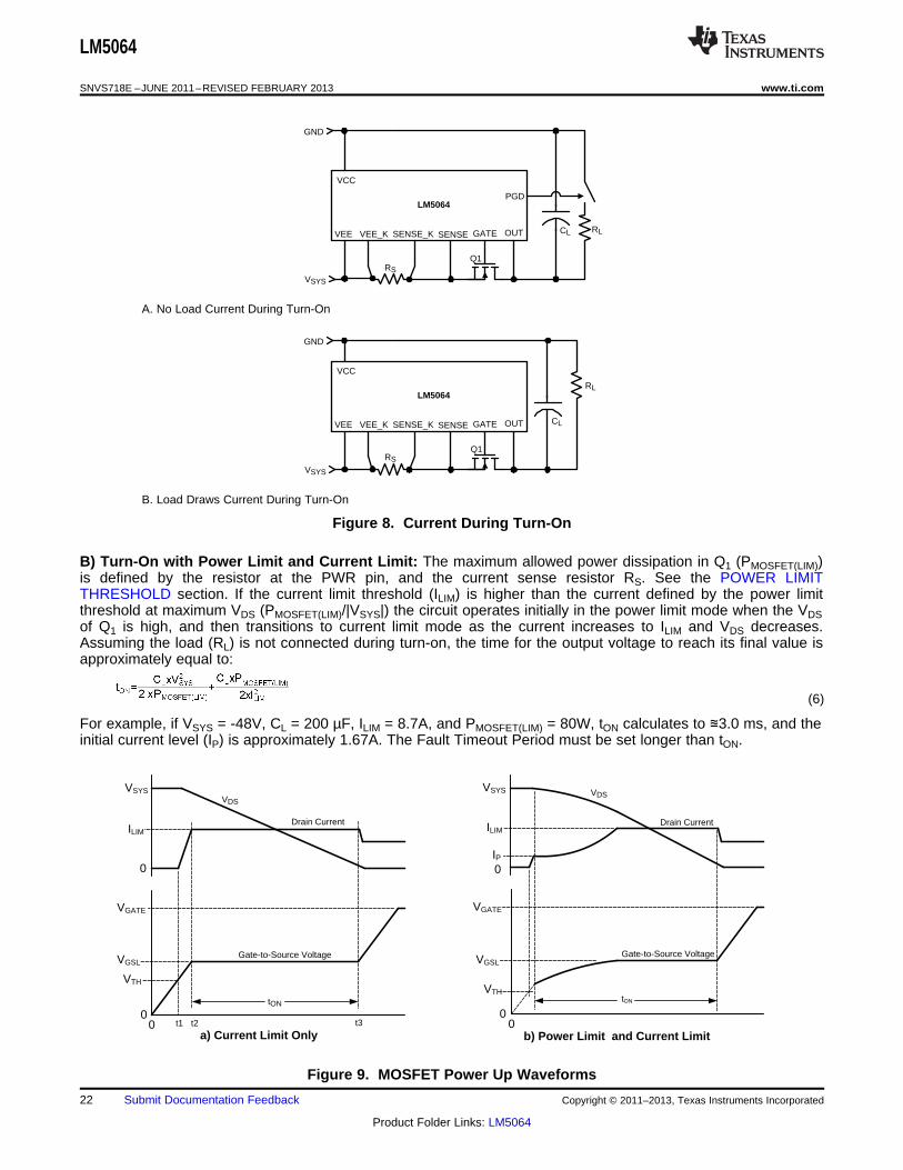
A. No Load Current During Turn-On
B. Load Draws Current During Turn-On
Figure 8. Current During Turn-On
B) Turn-On with Power Limit and Current Limit: The maximum allowed power dissipation in Q1 (PMOSFET(LIM))is defined by the resistor at the PWR pin, and the current sense resistor RS. See the POWER LIMITTHRESHOLD section. If the current limit threshold (ILIM) is higher than the current defined by the power limitthreshold at maximum VDS (PMOSFET(LIM)/|VSYS|) the circuit operates initially in the power limit mode when the VDSof Q1 is high, and then transitions to current limit mode as the current increases to ILIM and VDS decreases.Assuming the load (RL) is not connected during turn-on, the time for the output voltage to reach its final value isapproximately equal to:
(6)
For example, if VSYS = -48V, CL = 200 µF, ILIM = 8.7A, and PMOSFET(LIM) = 80W, tON calculates to ≊3.0 ms, and theinitial current level (IP) is approximately 1.67A. The Fault Timeout Period must be set longer than tON.
Figure 9. MOSFET Power Up Waveforms
22 Submit Documentation Feedback Copyright © 2011–2013, Texas Instruments Incorporated
Product Folder Links: LM5064

LM5064
www.ti.com SNVS718E –JUNE 2011–REVISED FEBRUARY 2013
TIMER CAPACITOR, CT
The TIMER pin capacitor (CT) sets the timing for the insertion time delay, fault timeout period, and the restarttiming of the LM5064.
A) Insertion Delay -Upon applying the system voltage (VSYS) to the circuit, the external MOSFET (Q1) is held offduring the insertion time (t1 in Figure 2) to allow ringing and transients at VSYS to settle. Since each backplane’sresponse to a circuit card plug-in is unique, the worst case settling time must be determined for each application.The insertion time starts when VSYS reaches the POR threshold, at which time the internal 4.8 µA current sourcecharges CT from 0V to 3.9V. The required capacitor value is calculated from:
(7)
For example, if the desired insertion delay is 125 ms, CT calculates to 0.15 µF. At the end of the insertion delay,CT is quickly discharged by a 1.5 mA current sink.
B) Fault Timeout Period -During in-rush current limiting or upon detection of a fault condition where the currentlimit and/or power limit circuits regulate the current through Q1, the fault timer current source (74 µA) is switchedon to charge CT. The Fault Timeout Period is the time required for the TIMER pin voltage to reach 3.9V, at whichtime Q1 is switched off. The required capacitor value for the desired Fault Timeout Period tFAULT is calculatedfrom:
(8)
For example, if the desired Fault Timeout Period is 8 ms, CT calculates to 0.15 µF. CT is discharged by the 2.4µA current sink at the end of the Fault Timeout Period. After the Fault Timeout Period, if RETRY = VDD, theLM5064 latches the GATE pin low until a power up sequence is initiated by external circuitry. When the FaultTimeout Period of the LM5064 expires, a restart sequence starts as described below (Restart Timing). Duringconsecutive cycles of the restart sequence, the fault timeout period is shorter than the initial fault time out perioddescribed above by approximately 8% since the voltage at the TIMER pin starts ramping up from 0.3V ratherthan VEE.
Since the LM5064 normally operates in power limit and/or current limit during a power up sequence, the FaultTimeout Period MUST be longer than the time required for the output voltage to reach its final value. See theTURN-ON TIME section.
C) Restart Timing For the LM5064, after the Fault Timeout Period described above, CT is discharged by the 2.4µA current sink to 1.2V. The TIMER pin then cycles through seven additional charge/discharge cycles between1.2V and 3.9V as shown in Figure 4. The restart time ends when the TIMER pin voltage reaches 0.3V during thefinal high-to-low ramp. The restart time, after the Fault Timeout Period, is equal to:
(9)= CT x 9.6 x 10⁶ (10)
For example, if CT = 0.15 µF, tRESTART = 1.4 seconds. At the end of the restart time, Q1 is switched on. If the faultis still present, the fault timeout and restart sequence repeats. The on-time duty cycle of Q1 is approximately0.5% in this mode.
UVLO, OVLO
By programming the UVLO and OVLO thresholds the LM5064 enables the series pass device (Q1) when theinput supply voltage (VSYS) is within the desired operational range. If VCC is below the UVLO threshold, or abovethe OVLO threshold, Q1 is switched off, denying power to the load. Hysteresis is provided for each threshold.
Copyright © 2011–2013, Texas Instruments Incorporated Submit Documentation Feedback 23
Product Folder Links: LM5064

VCC
UVLO/EN
OVLO
VEE
R1
R2
R3
2.48V
2.47V
TIMER AND GATELOGIC CONTROL
LM506420 PA
21 PA
VSYS
LM5064
SNVS718E –JUNE 2011–REVISED FEBRUARY 2013 www.ti.com
Option A: The configuration shown in Figure 10 requires three resistors (R1-R3) to set the thresholds.
Figure 10. UVLO and OVLO Thresholds Set By R1-R3
The procedure to calculate the resistor values is as follows:
- Choose the upper UVLO threshold (VUVH), and the lower UVLO threshold (VUVL).
- Choose the upper OVLO threshold (VOVH).
- The lower OVLO threshold (VOVL) cannot be chosen in advance in this case, but is determined after the valuesfor R1-R3 are determined. If VOVL must be accurately defined in addition to the other three thresholds, seeOption B below. The resistors are calculated as follows:
(11)
(12)
(13)
The lower OVLO threshold is calculated from:
(14)
As an example, assume the application requires the following thresholds: VUVH = 36V, VUVL = 32V, VOVH = 60V.
(15)
(16)
(17)
Using standard values of R1 = 200 kΩ, R2 = 8.87 kΩ, and R3 = 7.87 kΩ, the lower OVLO threshold calculates to56V, and the OVLO hysteresis is 4.4V. Note that the OVLO hysteresis is always slightly greater than the UVLOhysteresis in this configuration. When the R1-R3 resistor values are known, the threshold voltages andhysteresis are calculated from the following:
(18)
(19)VUV(HYS) = R1 x 20 µA (20)
(21)
(22)VOV(HYS) = (R1 + R2) x 21 µA (23)
24 Submit Documentation Feedback Copyright © 2011–2013, Texas Instruments Incorporated
Product Folder Links: LM5064

VCC
UVLO/EN
OVLO
VEE
R1
R2
R3
2.48V
2.47V
TIMER AND GATELOGIC CONTROL
LM5064
R4
GND20 PA
21 PA
VSYS
LM5064
www.ti.com SNVS718E –JUNE 2011–REVISED FEBRUARY 2013
Option B: If all four thresholds must be accurately defined, the configuration in Figure 11 can be used.
Figure 11. Programming the Four Thresholds
The four resistor values are calculated as follows: - Choose the upper and lower UVLO thresholds (VUVH) and(VUVL).
(24)
(25)
- Choose the upper and lower OVLO threshold (VOVH) and (VOVL).
(26)
(27)
As an example, assume the application requires the following thresholds: VUVH = 36V, VUVL = 32V, VOVH = 60V,and VOVL = 56V. Therefore VUV(HYS) = 4V, and VOV(HYS) = 4V. The resistor values are:
R1 = 200 kΩ, R2 = 16.8 kΩ
R3 = 190 kΩ, R4 = 8.2 kΩ
When the R1-R4 resistor values are known, the threshold voltages and hysteresis are calculated from thefollowing:
(28)
(29)VUV(HYS) = R1 x 20 µA (30)
(31)
(32)
Option C: The minimum UVLO level is obtained by connecting the UVLO/EN pin to VCC as shown in Figure 12.Q1 is switched on when the VCC-VEE voltage reaches the POREN threshold (≊8.7V). The OVLO thresholds areset using R3, R4. Their values are calculated using the procedure in Option B.
Copyright © 2011–2013, Texas Instruments Incorporated Submit Documentation Feedback 25
Product Folder Links: LM5064

PGD
PowerGood
LM5064
VEE
PGD
PowerGood
LM5064
VEE
PGD
PowerGood
LM5064
a) Delay Rising Edge Only b) Long delay at rising edge,short delay at falling edge
c) Short Delay at Rising Edge and LongDelay at Falling Edge, or Equal Delays
VEE
RPG
VPGD
CPG
VPGD VPGD
CPGRPG2
RPG1
CPG
RPG2
RPG1
VPGD
VEE
PGD
RPG
PowerGood
LM5064
VCC
UVLO/EN
OVLO
VEE
50k
R3
2.48V
2.47V
21 PA
TIMER ANDGATE LOGICCONTROL
LM5064
R4
GND 20 PA
Shutdown/RestartControl
VSYS
LM5064
SNVS718E –JUNE 2011–REVISED FEBRUARY 2013 www.ti.com
Figure 12. UVLO/EN = POREN
Option D: The OVLO function can be disabled by connecting the OVLO pin to VEE. The UVLO thresholds areset as described in Option B or Option C.
POWER GOOD PIN (PGD)
When the Q1 VDS voltage is below its threshold, the internal pull-down acting on the PGD pin is disabled,allowing PGD to rise to VPGD through the pull-up resistor, RPG, as shown in Figure 13. The pull-up voltage (VPGD)can be as high as 80V, and can be higher or lower than the voltages at VCC and OUT. VDD is a convenientchoice for VPGD as it allows interface to low voltage logic and avoids glitching on PGD during power up. If a delayis required at PGD, suggested circuits are shown in Figure 14. In Figure 14(A), capacitor CPG adds delay to therising edge, but not to the falling edge. In Figure 14(B), the rising edge is delayed by RPG1 + RPG2 and CPG, whilethe falling edge is delayed a lesser amount by RPG2 and CPG. Adding a diode across RPG2 (Figure 14 (C)) allowsfor equal delays at the two edges, or a short delay at the rising edge and a long delay at the falling edge.
Figure 13. Power Good Output
Figure 14. Adding Delay to the Power Good Output Pin
26 Submit Documentation Feedback Copyright © 2011–2013, Texas Instruments Incorporated
Product Folder Links: LM5064

Load
VCC
GND
BACKPLANE
OUT
LIVE
Q1RS
GATESENSEVEE
VSYS
LM5064
- 48V
PLUG- IN BOARD
CLD1
Z1
LM5064
www.ti.com SNVS718E –JUNE 2011–REVISED FEBRUARY 2013
SYSTEM CONSIDERATIONS
Continued proper operation of the LM5064 hot swap circuit requires a voltage clamping element present on thesupply side of the connector into which the hot swap circuit is plugged in. A TVS (Transient Voltage Suppressor)is ideal, as depicted in Figure 15 as Z1. The TVS is necessary to absorb the voltage transient generatedwhenever the hot swap circuit shuts off the load current. If the TVS is not present, inductance in the supply lineswill generate a voltage transient at shutdown which can exceed the absolute maximum rating of the LM5064,resulting in its destruction. For low current solutions (<2A), a capacitor may be sufficient to limit the voltagesurge, however this comes at the expense of input surge current on card insertion.
If the load powered by the LM5064 hot swap circuit has inductive characteristics, a Schottky diode (D1) isrequired across the LM5064’s output, along with some load capacitance (CL). The capacitance and the diode arenecessary to limit the negative excursion at the OUT pin when the load current is shut off. If the OUT pintransitions more than 0.3V negative the LM5064 can be permanently damaged. See Figure 15.
Figure 15. Output Diode Required for Inductive Loads
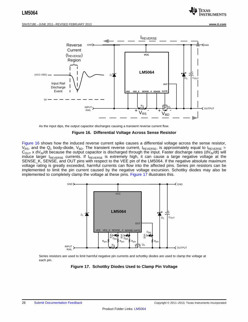
System Considerations During Surge Events
The control MOSFET, Q1, has a body-diode, illustrated in Figure 16, where current can freely flow in the reversedirection. The most common cause of a reverse current is a discharge event at the input of the hot-swap circuitwhen the output capacitance discharges to the input. Normally, reverse current flow presents no issue for hot-swap devices during events such as shutdown and minor input power perturbations. However, extreme situationssuch as high energy lighting surge line disturbances can expose the hot-swap circuit to pulses of ultra fast - highamplitude reverse currents. It is common to observe current amplitudes on the order of 1000A in these situations.Figure 16 illustrates what an extreme input discharge event may look like and how it affects the circuit.
Copyright © 2011–2013, Texas Instruments Incorporated Submit Documentation Feedback 27
Product Folder Links: LM5064
VEE_K
VCC
OUT
VEE SENSESENSE_ K
OUTPUT
LM5064
RS Q1
GND
+
COUTZ1
INPUT RAIL
D1
GATE
V
EE
GND
Rpin
VE
E
DpinRpin Rpin
DpinRpin
VE
E
Dpin
VEE_K
VCC
OUT
VEE SENSESENSE_ K
OUTPUT
LM5064
RS Q1
GND
+
COUT
Z1
INPUT RAIL
D1
GATE
GND
(VCC-VEE)
0V
+ -VRS
Input Rail Discharge
Event
VBD+ -
IREVERSE
Reverse Current
(IREVERSE)Region
LM5064
SNVS718E –JUNE 2011–REVISED FEBRUARY 2013 www.ti.com
As the input dips, the output capacitor discharges causing a transient reverse current flow.
Figure 16. Differential Voltage Across Sense Resistor
Figure 16 shows how the induced reverse current spike causes a differential voltage across the sense resistor,VRS, and the Q1 body-diode, VBD. The transient reverse current, IREVERSE, is approximately equal to IREVERSE =COUT x dVIN/dt because the output capacitor is discharged through the input. Faster discharge rates (dVIN/dt) willinduce larger IREVERSE currents. If IREVERSE is extremely high, it can cause a large negative voltage at theSENSE_K, SENSE, and OUT pins with respect to the VEE pin of the LM5064. If the negative absolute maximumvoltage rating is greatly exceeded, harmful currents can flow into the affected pins. Series pin resistors can beimplemented to limit the pin current caused by the negative voltage excursion. Schottky diodes may also beimplemented to completely clamp the voltage at these pins. Figure 17 illustrates this.
Series resistors are used to limit harmful negative pin currents and schottky diodes are used to clamp the voltage ateach pin.
Figure 17. Schottky Diodes Used to Clamp Pin Voltage
28 Submit Documentation Feedback Copyright © 2011–2013, Texas Instruments Incorporated
Product Folder Links: LM5064

LM5064
www.ti.com SNVS718E –JUNE 2011–REVISED FEBRUARY 2013
A typical value of Rpin can be 22Ω to effectively limit the pin current during extreme negative voltage spikes. Ifschottky diodes are used, they only need to be applied to SENSE_K, SENSE, and OUT. Each schottky diodereturn pin should be coupled closely with the VEE plane to provide the most effective clamping. The schottkydiode at OUT should be able to withstand at least 100V. VEE_K needs a series resistor even though it’s notsubjected to negative voltage spikes in order to balance the differential current sense voltage signal. Protectingthe SENSE_K, SENSE, and OUT pins from negative voltage spikes will facilitate a robust hot-swap circuit andsmooth operation during extreme reverse current surge events.
PC BOARD GUIDELINES
The following guidelines should be followed when designing the PC board for the LM5064:
- Place the LM5064 close to the board’s input connector to minimize trace inductance from the connector to theMOSFET (Q1).
- Place a TVS (Z1), directly adjacent to the VCC and VEE pins of the LM5064 to help minimize voltage transientswhich may occur on the input supply line. The TVS should be chosen such that the peak VSYS is just lower theTVS reverse-bias voltage. Transients of 20 volts or greater over the nominal input voltage can easily occur whenthe load current is shut off. A small capacitor may be sufficient for low current sense applications (I < 2A). It isrecommended to test the VSYS input voltage transient performance of the circuit by current limiting or shorting theload and measuring the peak input voltage transient.
- Place a 1 µF ceramic capacitor as close as possible to VREF pin.
- Place a 1 µF ceramic capacitor as close as possible to VDD pin.
- Minimize the inductance between the SENSE, SENSE_K, VEE_K, and VEE pins. There are anti-parallel diodesbetween these pins so any voltage greater than 0.3V in either polarity will cause significant current flow throughthe diodes, which can result in device failure. Do not place any resistors between these nodes.
- Minimize the impedance between the VEE_K and SENSE_K pins. There are anti-parallel diodes between thesepins so any voltage greater than 0.3V in either polarity will cause significant current flow through the diodes,which can result in device failure.
- The sense resistor (RS) should be placed close to the LM5064. A trace should connect the VEE source pin andOUT drain pad of Q1 to the sense resistor to VEE_K and SENSE_K pins, respectively. Connect RS using theKelvin techniques shown in Figure 7.
- The high current path from the board’s input to the load (via Q1), and the return path, should be parallel andclose to each other to minimize loop inductance.
- The termination connections for the various components around the LM5064 should be connected directly toeach other, and to the LM5064’s VEE pin connection, and then connected to VSYS at one point. Do not connectthe various component terminations to each other through the high current VSYS line.
- Provide adequate thermal sinking for the series pass device (Q1) to help reduce stresses during turn-on andturn-off.
- The board’s edge connector can be designed such that the LM5064 detects via the UVLO/EN pin that theboard is being removed, and responds by turning off the load before the supply voltage is disconnected. Forexample, in Figure 18, the voltage at the UVLO/EN pin goes to VEE before VSYS is removed from the LM5064 asa result of the shorter edge connector pin. When the board is inserted into the edge connector, the systemvoltage is applied to the LM5064’s VSYS pin before the UVLO voltage is taken high, thereby allowing the LM5064to turn on the output in a controlled fashion.
Copyright © 2011–2013, Texas Instruments Incorporated Submit Documentation Feedback 29
Product Folder Links: LM5064
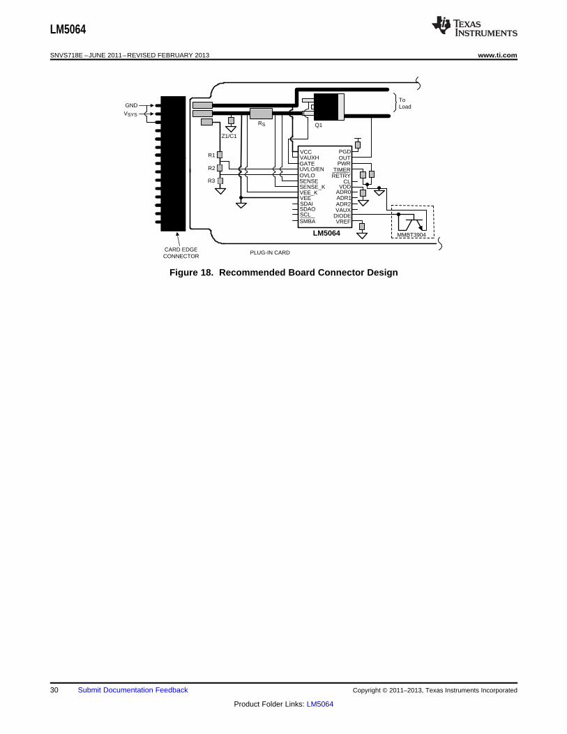
Q1
Z1/C1
R2
R3
ToLoad
RS
CARD EDGE CONNECTOR
PLUG-IN CARD
VSYS
GND
VCC PGD
VREF
OUTPWR
SCLSMBA
DIODEVAUXADR2
GATEVAUXH
UVLO/EN
SENSESENSE_KVEE_K
SDAI
TIMERRETRY
CLVDD
ADR0ADR1
LM5064
OVLO
VEE
SDAO
MMBT3904
R1
LM5064
SNVS718E –JUNE 2011–REVISED FEBRUARY 2013 www.ti.com
Figure 18. Recommended Board Connector Design
30 Submit Documentation Feedback Copyright © 2011–2013, Texas Instruments Incorporated
Product Folder Links: LM5064
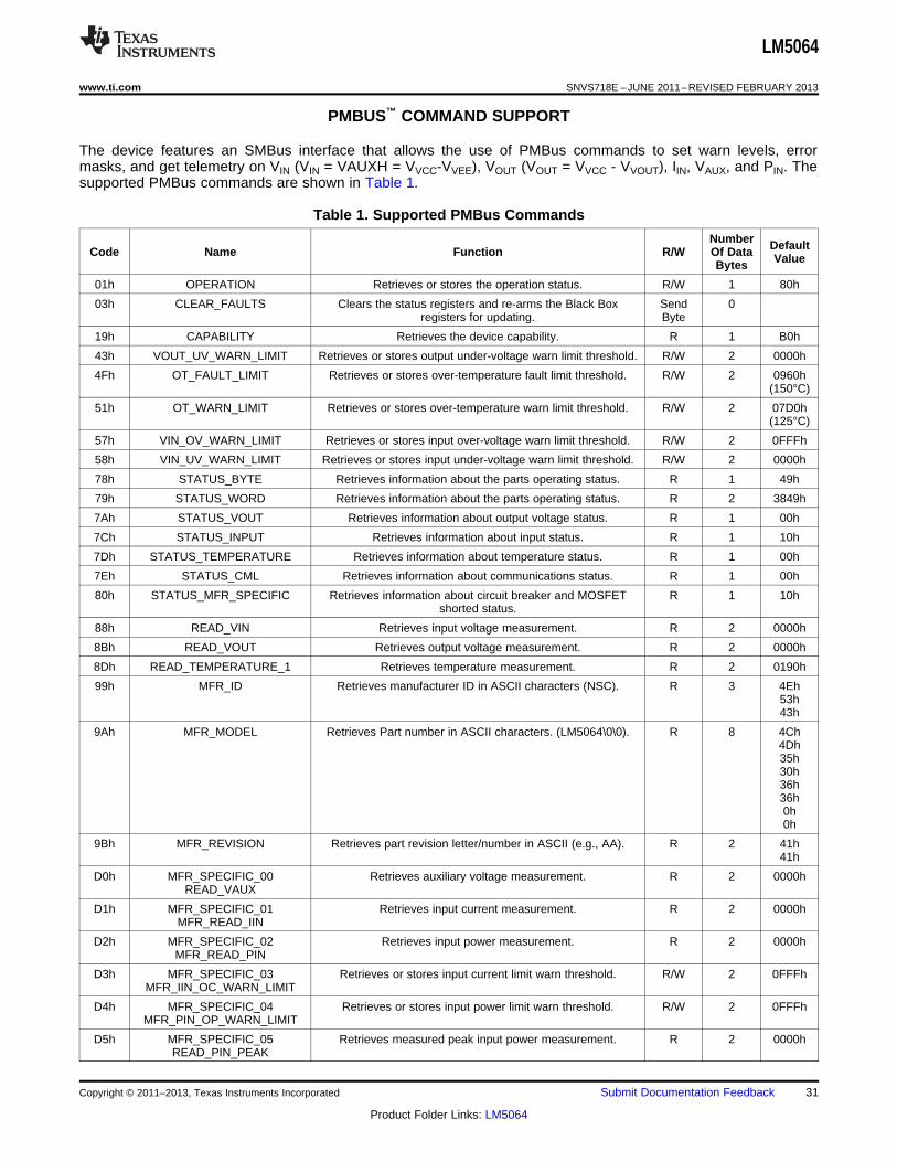
LM5064
www.ti.com SNVS718E –JUNE 2011–REVISED FEBRUARY 2013
PMBUS™ COMMAND SUPPORT
The device features an SMBus interface that allows the use of PMBus commands to set warn levels, errormasks, and get telemetry on VIN (VIN = VAUXH = VVCC-VVEE), VOUT (VOUT = VVCC - VVOUT), IIN, VAUX, and PIN. Thesupported PMBus commands are shown in Table 1.
Table 1. Supported PMBus Commands
Number DefaultCode Name Function R/W Of Data ValueBytes
01h OPERATION Retrieves or stores the operation status. R/W 1 80h
03h CLEAR_FAULTS Clears the status registers and re-arms the Black Box Send 0registers for updating. Byte
19h CAPABILITY Retrieves the device capability. R 1 B0h
43h VOUT_UV_WARN_LIMIT Retrieves or stores output under-voltage warn limit threshold. R/W 2 0000h
4Fh OT_FAULT_LIMIT Retrieves or stores over-temperature fault limit threshold. R/W 2 0960h(150°C)
51h OT_WARN_LIMIT Retrieves or stores over-temperature warn limit threshold. R/W 2 07D0h(125°C)
57h VIN_OV_WARN_LIMIT Retrieves or stores input over-voltage warn limit threshold. R/W 2 0FFFh
58h VIN_UV_WARN_LIMIT Retrieves or stores input under-voltage warn limit threshold. R/W 2 0000h
78h STATUS_BYTE Retrieves information about the parts operating status. R 1 49h
79h STATUS_WORD Retrieves information about the parts operating status. R 2 3849h
7Ah STATUS_VOUT Retrieves information about output voltage status. R 1 00h
7Ch STATUS_INPUT Retrieves information about input status. R 1 10h
7Dh STATUS_TEMPERATURE Retrieves information about temperature status. R 1 00h
7Eh STATUS_CML Retrieves information about communications status. R 1 00h
80h STATUS_MFR_SPECIFIC Retrieves information about circuit breaker and MOSFET R 1 10hshorted status.
88h READ_VIN Retrieves input voltage measurement. R 2 0000h
8Bh READ_VOUT Retrieves output voltage measurement. R 2 0000h
8Dh READ_TEMPERATURE_1 Retrieves temperature measurement. R 2 0190h
99h MFR_ID Retrieves manufacturer ID in ASCII characters (NSC). R 3 4Eh53h43h
9Ah MFR_MODEL Retrieves Part number in ASCII characters. (LM5064\0\0). R 8 4Ch4Dh35h30h36h36h0h0h
9Bh MFR_REVISION Retrieves part revision letter/number in ASCII (e.g., AA). R 2 41h41h
D0h MFR_SPECIFIC_00 Retrieves auxiliary voltage measurement. R 2 0000hREAD_VAUX
D1h MFR_SPECIFIC_01 Retrieves input current measurement. R 2 0000hMFR_READ_IIN
D2h MFR_SPECIFIC_02 Retrieves input power measurement. R 2 0000hMFR_READ_PIN
D3h MFR_SPECIFIC_03 Retrieves or stores input current limit warn threshold. R/W 2 0FFFhMFR_IIN_OC_WARN_LIMIT
D4h MFR_SPECIFIC_04 Retrieves or stores input power limit warn threshold. R/W 2 0FFFhMFR_PIN_OP_WARN_LIMIT
D5h MFR_SPECIFIC_05 Retrieves measured peak input power measurement. R 2 0000hREAD_PIN_PEAK
Copyright © 2011–2013, Texas Instruments Incorporated Submit Documentation Feedback 31
Product Folder Links: LM5064
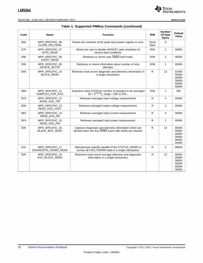
LM5064
SNVS718E –JUNE 2011–REVISED FEBRUARY 2013 www.ti.com
Table 1. Supported PMBus Commands (continued)
Number DefaultCode Name Function R/W Of Data ValueBytes
D6h MFR_SPECIFIC_06 Resets the contents of the peak input power register to zero. Send 0CLEAR_PIN_PEAK Byte
D7h MFR_SPECIFIC_07 Allows the user to disable MOSFET gate shutdown for R/W 1 0000hGATE_MASK various fault conditions.
D8h MFR_SPECIFIC_08 Retrieves or stores user SMBA fault mask. R/W 2 0820hALERT_MASK
D9h MFR_SPECIFIC_09 Retrieves or stores information about number of retry R/W 1 0000hDEVICE_SETUP attempts.
DAh MFR_SPECIFIC_10 Retrieves most recent diagnostic and telemetry information in R 12 0190hBLOCK_READ a single transaction. 0000h
0000h0000h0000h0000h
DBh MFR_SPECIFIC_11 Exponent value AVGN for number of samples to be averaged R/W 1 00hSAMPLES_FOR_AVG (N = 2AVGN), range = 00h to 0Ch .
DCh MFR_SPECIFIC_12 Retrieves averaged input voltage measurement. R 2 0000hREAD_AVG_VIN
DDh MFR_SPECIFIC_13 Retrieves averaged output voltage measurement. R 2 0000hREAD_AVG_VOUT
DEh MFR_SPECIFIC_14 Retrieves averaged input current measurement. R 2 0000hREAD_AVG_IIN
DFh MFR_SPECIFIC_15 Retrieves averaged input power measurement. R 2 0000hREAD_AVG_PIN
E0h MFR_SPECIFIC_16 Captures diagnostic and telemetry information which are R 12 0000hBLACK_BOX_READ latched when the first SMBA event after faults are cleared. 0000h
0000h0000h0000h0000h
E1h MFR_SPECIFIC_17 Manufacturer-specific parallel of the STATUS_WORD to R 2 08E0hDIAGNOSTIC_WORD_READ convey all FAULT/WARN data in a single transaction.
E2h MFR_SPECIFIC_18 Retrieves most recent average telemetry and diagnostic R 12 0000hAVG_BLOCK_READ information in a single transaction. 0000h
0000h0000h0000h0000h
32 Submit Documentation Feedback Copyright © 2011–2013, Texas Instruments Incorporated
Product Folder Links: LM5064

LM5064
www.ti.com SNVS718E –JUNE 2011–REVISED FEBRUARY 2013
STANDARD PMBUS COMMANDS
OPERATION (01h)
The OPERATION command is a standard PMBus command that controls the MOSFET switch. This commandmay be used to switch the MOSFET ON and OFF under host control. It is also used to re-enable the MOSFETafter a fault triggered shutdown. Writing an OFF command, followed by an ON command, will clear all faults andre-enable the device. Writing only an ON after a fault-triggered shutdown will not clear the fault registers or re-enable the device. The OPERATION command is issued with the write byte protocol.
Table 2. Recognized OPERATION Command Values
Value Meaning Default
80h Switch ON 80h
00h Switch OFF n/a
CLEAR FAULTS (03h)
The CLEAR_FAULTS command is a standard PMBus command that resets all stored warning and fault flagsand the SMBA signal. If a fault or warning condition still exists when the CLEAR_FAULTS command is issued,the SMBA signal may not clear or will re-assert almost immediately. Issuing a CLEAR_FAULTS command willnot cause the MOSFET to switch back on in the event of a fault turnoff - that must be done by issuing anOPERATION command after the fault condition is cleared. This command uses the PMBus send byte protocol.
CAPABILITY (19h)
The CAPABILITY command is a standard PMBus command that returns information about the PMBus functionssupported by the LM5064. This command is read with the PMBus read byte protocol.
Table 3. CAPABILITY Register
Value Meaning Default
B0h Supports Packet Error Check, 400Kbits/sec, B0hSupports SMBus Alert
VOUT_UV_WARN_LIMIT (43h)
The VOUT_UV_WARN_LIMIT command is a standard PMBus command that allows configuring or reading thethreshold for the VOUT under-voltage Warning detection. Reading and writing to this register should use thecoefficients shown in Table 41. Accesses to this command should use the PMBus read or write word protocol. Ifthe measured value of VOUT falls below the value in this register, VOUT UV Warn flags are set and the SMBAsignal is asserted.
Table 4. VOUT_UV_WARN_LIMIT Register
Value Meaning Default
1h – 0FFFh VOUT Under-Voltage Warning detection 0000h (disabled)threshold
0000h VOUT Under-Voltage Warning disabled n/a
OT_FAULT_LIMIT (4Fh)
The OT_FAULT_LIMIT command is a standard PMBus command that allows configuring or reading the thresholdfor the over-temperature fault detection. Reading and writing to this register should use the coefficients shown inTable 41. Accesses to this command should use the PMBus read or write word protocol. If the measuredtemperature exceeds this value, an over-temperature fault is triggered and the MOSFET is switched off, OTFAULT flags set, and the SMBA signal asserted. After the measured temperature falls below the value in thisregister, the MOSFET may be switched back on with the OPERATION command. A single temperaturemeasurement is an average of 16 round-robin cycles; therefore, the minimum temperature fault detection time is16 ms.
Copyright © 2011–2013, Texas Instruments Incorporated Submit Documentation Feedback 33
Product Folder Links: LM5064
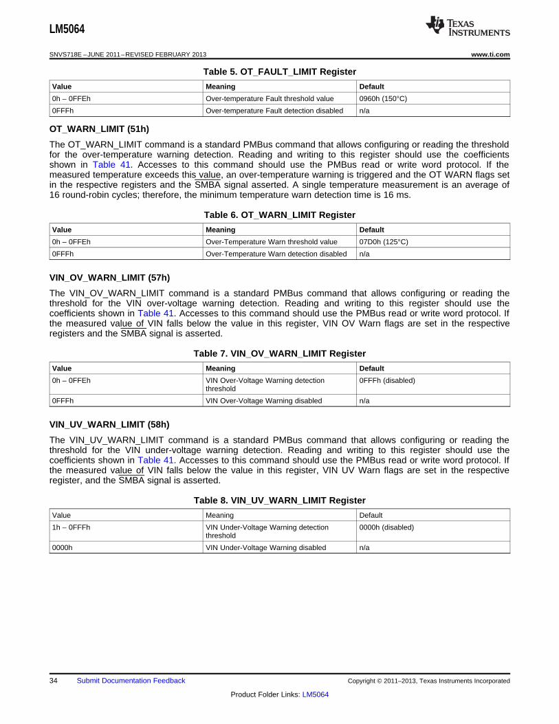
LM5064
SNVS718E –JUNE 2011–REVISED FEBRUARY 2013 www.ti.com
Table 5. OT_FAULT_LIMIT Register
Value Meaning Default
0h – 0FFEh Over-temperature Fault threshold value 0960h (150°C)
0FFFh Over-temperature Fault detection disabled n/a
OT_WARN_LIMIT (51h)
The OT_WARN_LIMIT command is a standard PMBus command that allows configuring or reading the thresholdfor the over-temperature warning detection. Reading and writing to this register should use the coefficientsshown in Table 41. Accesses to this command should use the PMBus read or write word protocol. If themeasured temperature exceeds this value, an over-temperature warning is triggered and the OT WARN flags setin the respective registers and the SMBA signal asserted. A single temperature measurement is an average of16 round-robin cycles; therefore, the minimum temperature warn detection time is 16 ms.
Table 6. OT_WARN_LIMIT Register
Value Meaning Default
0h – 0FFEh Over-Temperature Warn threshold value 07D0h (125°C)
0FFFh Over-Temperature Warn detection disabled n/a
VIN_OV_WARN_LIMIT (57h)
The VIN_OV_WARN_LIMIT command is a standard PMBus command that allows configuring or reading thethreshold for the VIN over-voltage warning detection. Reading and writing to this register should use thecoefficients shown in Table 41. Accesses to this command should use the PMBus read or write word protocol. Ifthe measured value of VIN falls below the value in this register, VIN OV Warn flags are set in the respectiveregisters and the SMBA signal is asserted.
Table 7. VIN_OV_WARN_LIMIT Register
Value Meaning Default
0h – 0FFEh VIN Over-Voltage Warning detection 0FFFh (disabled)threshold
0FFFh VIN Over-Voltage Warning disabled n/a
VIN_UV_WARN_LIMIT (58h)
The VIN_UV_WARN_LIMIT command is a standard PMBus command that allows configuring or reading thethreshold for the VIN under-voltage warning detection. Reading and writing to this register should use thecoefficients shown in Table 41. Accesses to this command should use the PMBus read or write word protocol. Ifthe measured value of VIN falls below the value in this register, VIN UV Warn flags are set in the respectiveregister, and the SMBA signal is asserted.
Table 8. VIN_UV_WARN_LIMIT Register
Value Meaning Default
1h – 0FFFh VIN Under-Voltage Warning detection 0000h (disabled)threshold
0000h VIN Under-Voltage Warning disabled n/a
34 Submit Documentation Feedback Copyright © 2011–2013, Texas Instruments Incorporated
Product Folder Links: LM5064

LM5064
www.ti.com SNVS718E –JUNE 2011–REVISED FEBRUARY 2013
STATUS_BYTE (78h)
The STATUS BYTE is a standard PMBus command that returns the value of a number of flags indicating thestate of the LM5064. Accesses to this command should use the PMBus read byte protocol. To clear bits in thisregister, the underlying fault should be removed on the system and a CLEAR_FAULTS command issued.
Table 9. STATUS_BYTE Definitions
Bit NAME Meaning Default
7 BUSY Not Supported, always 0 0
6 OFF This bit is asserted if the MOSFET is not switched on 1for any reason.
5 VOUT OV Not Supported, always 0 0
4 IOUT OC Not Supported, always 0 0
3 VIN UV FAULT A VIN Under-Voltage Fault has occurred 1
2 TEMPERATURE A Temperature Fault or Warning has occurred 0
1 CML A Communication Fault has occurred 0
0 None of the Above A fault or warning not listed in bits [7:1] has occurred 1
STATUS_WORD (79h)
The STATUS_WORD command is a standard PMBus command that returns the value of a number of flagsindicating the state of the LM5064. Accesses to this command should use the PMBus read word protocol. Toclear bits in this register, the underlying fault should be removed and a CLEAR _FAULTS command issued. TheINPUT and VIN UV flags will default to 1 on startup, however, they will be cleared to 0 after the first time theinput voltage exceeds the resistor-programmed UVLO threshold.
Table 10. STATUS_WORD Definitions
Bit NAME Meaning Default
15 VOUT An output voltage fault or warning has occurred 0
14 IOUT/POUT Not Supported, always 0 0
13 INPUT An input voltage or current fault has occurred 1
12 MFR A Manufacturer Specific Fault or Warning has occurred 1
11 POWER GOOD The Power Good signal has been negated 1
10 FANS Not Supported, always 0 0
9 OTHER Not Supported, always 0 0
8 UNKNOWN Not Supported, always 0 0
7 BUSY Not Supported, always 0 0
6 OFF This bit is asserted if the MOSFET is not switched on for 1any reason.
5 VOUT OV Not Supported, always 0 0
4 IOUT OC Not Supported, always 0 0
3 VIN UV FAULT A VIN Under-Voltage Fault has occurred 1
2 TEMPERATURE A Temperature Fault or Warning has occurred 0
1 CML A Communication Fault has occurred 0
0 None of the Above A fault or warning not listed in bits [7:1] has occurred 1
Copyright © 2011–2013, Texas Instruments Incorporated Submit Documentation Feedback 35
Product Folder Links: LM5064

LM5064
SNVS718E –JUNE 2011–REVISED FEBRUARY 2013 www.ti.com
STATUS_VOUT (7Ah)
The STATUS_VOUT command is a standard PMBus command that returns the value of the VOUT UV Warnflag. Accesses to this command should use the PMBus read byte protocol. To clear bits in this register, theunderlying fault should be cleared and a CLEAR_FAULTS command issued.
Table 11. STATUS_VOUT Definitions
Bit NAME Meaning Default
7 VOUT OV Fault Not Supported, always 0 0
6 VOUT OV Warn Not Supported, always 0 0
5 VOUT UV Warn A VOUT Under-Voltage Warning has occurred 0
4 VOUT UV Fault Not Supported, always 0 0
3 VOUT Max Not Supported, always 0 0
2 TON Max Fault Not Supported, always 0 0
1 TOFF Max Fault Not Supported, always 0 0
0 VOUT Tracking Error Not Supported, always 0 0
STATUS_INPUT (7Ch)
The STATUS_INPUT command is a standard PMBus command that returns the value of a number of flagsrelated to input voltage, current, and power. Accesses to this command should use the PMBus read byteprotocol. To clear bits in this register, the underlying fault should be cleared and a CLEAR_FAULTS commandissued. The VIN UV Warn flag will default to 1 on startup, however, it will be cleared to 0 after the first time theinput voltage increases above the resistor-programmed UVLO threshold.
Table 12. STATUS_INPUT Definitions
Bit NAME Meaning Default
7 VIN OV Fault A VIN Over-Voltage Fault has occurred 0
6 VIN OV Warn A VIN Over-Voltage Warning has occurred 0
5 VIN UV Warn A VIN Under-Voltage Warning has occurred 1
4 VIN UV Fault A VIN Under-Voltage Fault has occurred 0
3 Insufficient Voltage Not Supported, always 0 0
2 IIN OC Fault An IIN Over-Current Fault has occurred 0
1 IIN OC Warn An IIN Over-Current Warning has occurred 0
0 PIN OP Warn A PIN Over-Power Warning has occurred 0
STATUS_TEMPERATURE (7dh)
The STATUS_TEMPERATURE is a standard PMBus command that returns the value of the of a number of flagsrelated to the temperature telemetry value. Accesses to this command should use the PMBus read byte protocol.To clear bits in this register, the underlying fault should be cleared and a CLEAR_FAULTS command issued.
Table 13. STATUS_TEMPERATURE Definitions
Bit NAME Meaning Default
7 Overtemp Fault An Over-Temperature Fault has occurred 0
6 Overtemp Warn An Over-Temperature Warning has occurred 0
5 Undertemp Warn Not Supported, always 0 0
4 Undertemp Fault Not Supported, always 0 0
3 reserved Not Supported, always 0 0
2 reserved Not Supported, always 0 0
1 reserved Not Supported, always 0 0
0 reserved Not Supported, always 0 0
36 Submit Documentation Feedback Copyright © 2011–2013, Texas Instruments Incorporated
Product Folder Links: LM5064
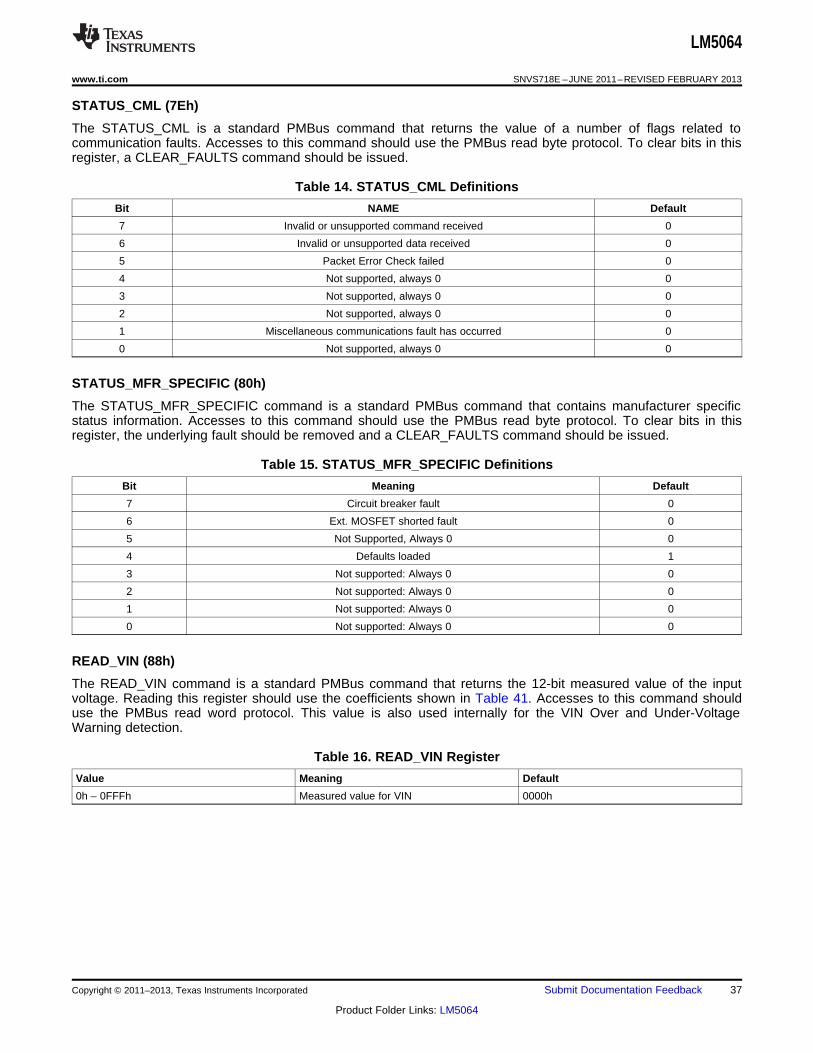
LM5064
www.ti.com SNVS718E –JUNE 2011–REVISED FEBRUARY 2013
STATUS_CML (7Eh)
The STATUS_CML is a standard PMBus command that returns the value of a number of flags related tocommunication faults. Accesses to this command should use the PMBus read byte protocol. To clear bits in thisregister, a CLEAR_FAULTS command should be issued.
Table 14. STATUS_CML Definitions
Bit NAME Default
7 Invalid or unsupported command received 0
6 Invalid or unsupported data received 0
5 Packet Error Check failed 0
4 Not supported, always 0 0
3 Not supported, always 0 0
2 Not supported, always 0 0
1 Miscellaneous communications fault has occurred 0
0 Not supported, always 0 0
STATUS_MFR_SPECIFIC (80h)
The STATUS_MFR_SPECIFIC command is a standard PMBus command that contains manufacturer specificstatus information. Accesses to this command should use the PMBus read byte protocol. To clear bits in thisregister, the underlying fault should be removed and a CLEAR_FAULTS command should be issued.
Table 15. STATUS_MFR_SPECIFIC Definitions
Bit Meaning Default
7 Circuit breaker fault 0
6 Ext. MOSFET shorted fault 0
5 Not Supported, Always 0 0
4 Defaults loaded 1
3 Not supported: Always 0 0
2 Not supported: Always 0 0
1 Not supported: Always 0 0
0 Not supported: Always 0 0
READ_VIN (88h)
The READ_VIN command is a standard PMBus command that returns the 12-bit measured value of the inputvoltage. Reading this register should use the coefficients shown in Table 41. Accesses to this command shoulduse the PMBus read word protocol. This value is also used internally for the VIN Over and Under-VoltageWarning detection.
Table 16. READ_VIN Register
Value Meaning Default
0h – 0FFFh Measured value for VIN 0000h
Copyright © 2011–2013, Texas Instruments Incorporated Submit Documentation Feedback 37
Product Folder Links: LM5064
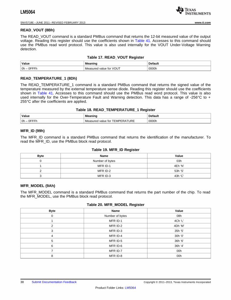
LM5064
SNVS718E –JUNE 2011–REVISED FEBRUARY 2013 www.ti.com
READ_VOUT (8Bh)
The READ_VOUT command is a standard PMBus command that returns the 12-bit measured value of the outputvoltage. Reading this register should use the coefficients shown in Table 41. Accesses to this command shoulduse the PMBus read word protocol. This value is also used internally for the VOUT Under-Voltage Warningdetection.
Table 17. READ_VOUT Register
Value Meaning Default
0h – 0FFFh Measured value for VOUT 0000h
READ_TEMPERATURE_1 (8Dh)
The READ_TEMPERATURE_1 command is a standard PMBus command that returns the signed value of thetemperature measured by the external temperature sense diode. Reading this register should use the coefficientsshown in Table 41. Accesses to this command should use the PMBus read word protocol. This value is alsoused internally for the Over-Temperature Fault and Warning detection. This data has a range of -256°C to +255°C after the coefficients are applied.
Table 18. READ_TEMPERATURE_1 Register
Value Meaning Default
0h – 0FFFh Measured value for TEMPERATURE 0000h
MFR_ID (99h)
The MFR_ID command is a standard PMBus command that returns the identification of the manufacturer. Toread the MFR_ID, use the PMBus block read protocol.
Table 19. MFR_ID Register
Byte Name Value
0 Number of bytes 03h
1 MFR ID-1 4Eh ‘N’
2 MFR ID-2 53h ‘S’
3 MFR ID-3 43h ‘C’
MFR_MODEL (9Ah)
The MFR_MODEL command is a standard PMBus command that returns the part number of the chip. To readthe MFR_MODEL, use the PMBus block read protocol.
Table 20. MFR_MODEL Register
Byte Name Value
0 Number of bytes 08h
1 MFR ID-1 4Ch ‘L’
2 MFR ID-2 4Dh ‘M’
3 MFR ID-3 35h ‘5’
4 MFR ID-4 30h ‘0’
5 MFR ID-5 36h ‘6’
6 MFR ID-6 36h ‘4’
7 MFR ID-7 00h
8 MFR ID-8 00h
38 Submit Documentation Feedback Copyright © 2011–2013, Texas Instruments Incorporated
Product Folder Links: LM5064

LM5064
www.ti.com SNVS718E –JUNE 2011–REVISED FEBRUARY 2013
MFR_REVISION (9Bh)
The MFR_REVISION command is a standard PMBus command that returns the revision level of the part. Toread the MFR_REVISION, use the PMBus block read protocol.
Table 21. MFR_REVISION Register
Byte Name Value
0 Number of bytes 02h
1 MFR ID-1 41h ‘A’
2 MFR ID-2 41h ‘A’
Copyright © 2011–2013, Texas Instruments Incorporated Submit Documentation Feedback 39
Product Folder Links: LM5064

LM5064
SNVS718E –JUNE 2011–REVISED FEBRUARY 2013 www.ti.com
MANUFACTURER SPECIFIC PMBUS™ COMMANDS
MFR_SPECIFIC_00: READ_VAUX (D0h)
The READ_VAUX command will report the 12-bit ADC measured auxiliary voltage. Voltages greater than orequal to 2.97V to VEE will be reported at plus full scale (0FFFh). Voltages less than or equal to 0V referenced toVEE will be reported as 0 (0000h). To read data from the READ_VAUX command, use the PMBus Read Wordprotocol.
Table 22. READ_VAUX Register
Value Meaning Default
0h – 0FFFh Measured value for VAUX input 0000h
MFR_SPECIFIC_01: MFR_READ_IIN (D1h)
The MFR_READ_IIN command will report the 12-bit ADC measured current sense voltage. To read data fromthe MFR_READ_IIN command, use the PMBus Read Word protocol. Reading this register should use thecoefficients shown in Table 41. Please see the section on coefficient calculations to calculate the values to use.
Table 23. MFR_READ_IIN Register
Value Meaning Default
0h – 0FFFh Measured value for input current sense 0000hvoltage
MFR_SPECIFIC_02: MFR_READ_PIN (D2h)
The MFR_READ_PIN command will report the upper 12 bits of the VIN x IIN product as measured by the 12-bitADC. To read data from the MFR_READ_PIN command, use the PMBus Read Word protocol. Reading thisregister should use the coefficients shown in Table 41. Please see the section on coefficient calculations tocalculate the values to use.
Table 24. MFR_READ_PIN Register
Value Meaning Default
0h – 0FFFh Value for input current x input voltage 0000h
MFR_SPECIFIC_03: MFR_IN_OC_WARN_LIMIT (D3h)
The MFR_IIN_OC_WARN_LIMIT PMBus command sets the input over-current warning threshold. In the eventthat the input current rises above the value set in this register, the IIN over-current flags are set in the respectiveregisters and the SMBA is asserted. To access the MFR_IIN_OC_WARN_LIMIT register, use the PMBusRead/Write Word protocol. Reading/writing to this register should use the coefficients shown in Table 41.
Table 25. MFR_IIN_OC_WARN_LIMIT Register
Value Meaning Default
0h – 0FFEh Value for input over-current warn limit 0FFFh
0FFFh Input over-current warning disabled n/a
40 Submit Documentation Feedback Copyright © 2011–2013, Texas Instruments Incorporated
Product Folder Links: LM5064

LM5064
www.ti.com SNVS718E –JUNE 2011–REVISED FEBRUARY 2013
MFR_SPECIFIC_04: MFR_PIN_OP_WARN_LIMIT (D4h)
The MFR_PIN_OP_WARN_LIMIT PMBus command sets the input over-power warning threshold. In the eventthat the input power rises above the value set in this register, the PIN over-power flags are set in the respectiveregisters and the SMBA is asserted. To access the MFR_PIN_OP_WARN_LIMIT register, use the PMBusRead/Write Word protocol. Reading/writing to this register should use the coefficients shown in Table 41.
Table 26. MFR_PIN_OPWARN_LIMIT Register
Value Meaning Default
0h – 0FFEh Value for input over-power warn limit 0FFFh
0FFFh Input over-power warning disabled n/a
MFR_SPECIFIC_05: READ_PIN_PEAK (D5h)
The READ_PIN_PEAK command will report the maximum input power measured since a Power On reset or thelast CLEAR_PIN_PEAK command. To access the READ_PIN_PEAK command, use the PMBus Read Wordprotocol. Use the coefficients shown in Table 41.
Table 27. READ_PIN_PEAK Register
Value Meaning Default
0h – 0FFEh Maximum Value for input current x input 0hvoltage since reset or last clear
MFR_SPECIFIC_06: CLEAR_PIN_PEAK (D6h)
The CLEAR_PIN_PEAK command will clear the PIN PEAK register. This command uses the PMBus Send Byteprotocol.
MFR_SPECIFIC_07: GATE_MASK (D7h)
The GATE_MASK register allows the hardware to prevent fault conditions from switching off the MOSFET. Whenthe bit is high, the corresponding FAULT has no control over the MOSFET gate. All status registers will still beupdated (STATUS, DIAGNOSTIC) and an SMBA will still be asserted. This register is accessed with the PMBusRead / Write Byte protocol.
The IIN/PFET Fault refers to the input current fault and the MOSFET power dissipation fault. There is no inputpower fault detection; only input power warning detection.
WARNING
Inhibiting the MOSFET switch off in response to over-current or circuit breakerfault conditions will likely result in the destruction of the MOSFET! Thisfunctionality should be used with great care and supervision!
Table 28. MFR_SPECIFIC_07 GATE MASK Definitions
Bit NAME Default
7 Not used, always 0 0
6 Not used, always 0 0
5 VIN UV FAULT 0
4 VIN OV FAULT 0
3 IIN/PFET FAULT 0
2 OVERTEMP FAULT 0
1 Not used, always 0 0
0 CIRCUIT BREAKER FAULT 0
Copyright © 2011–2013, Texas Instruments Incorporated Submit Documentation Feedback 41
Product Folder Links: LM5064
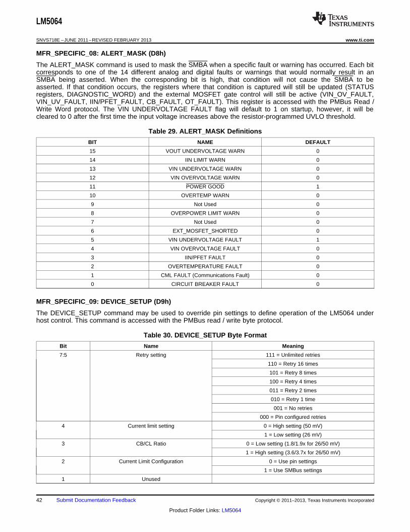
LM5064
SNVS718E –JUNE 2011–REVISED FEBRUARY 2013 www.ti.com
MFR_SPECIFIC_08: ALERT_MASK (D8h)
The ALERT_MASK command is used to mask the SMBA when a specific fault or warning has occurred. Each bitcorresponds to one of the 14 different analog and digital faults or warnings that would normally result in anSMBA being asserted. When the corresponding bit is high, that condition will not cause the SMBA to beasserted. If that condition occurs, the registers where that condition is captured will still be updated (STATUSregisters, DIAGNOSTIC_WORD) and the external MOSFET gate control will still be active (VIN_OV_FAULT,VIN_UV_FAULT, IIN/PFET_FAULT, CB_FAULT, OT_FAULT). This register is accessed with the PMBus Read /Write Word protocol. The VIN UNDERVOLTAGE FAULT flag will default to 1 on startup, however, it will becleared to 0 after the first time the input voltage increases above the resistor-programmed UVLO threshold.
Table 29. ALERT_MASK Definitions
BIT NAME DEFAULT
15 VOUT UNDERVOLTAGE WARN 0
14 IIN LIMIT WARN 0
13 VIN UNDERVOLTAGE WARN 0
12 VIN OVERVOLTAGE WARN 0
11 POWER GOOD 1
10 OVERTEMP WARN 0
9 Not Used 0
8 OVERPOWER LIMIT WARN 0
7 Not Used 0
6 EXT_MOSFET_SHORTED 0
5 VIN UNDERVOLTAGE FAULT 1
4 VIN OVERVOLTAGE FAULT 0
3 IIN/PFET FAULT 0
2 OVERTEMPERATURE FAULT 0
1 CML FAULT (Communications Fault) 0
0 CIRCUIT BREAKER FAULT 0
MFR_SPECIFIC_09: DEVICE_SETUP (D9h)
The DEVICE_SETUP command may be used to override pin settings to define operation of the LM5064 underhost control. This command is accessed with the PMBus read / write byte protocol.
Table 30. DEVICE_SETUP Byte Format
Bit Name Meaning
7:5 Retry setting 111 = Unlimited retries
110 = Retry 16 times
101 = Retry 8 times
100 = Retry 4 times
011 = Retry 2 times
010 = Retry 1 time
001 = No retries
000 = Pin configured retries
4 Current limit setting 0 = High setting (50 mV)
1 = Low setting (26 mV)
3 CB/CL Ratio 0 = Low setting (1.8/1.9x for 26/50 mV)
1 = High setting (3.6/3.7x for 26/50 mV)
2 Current Limit Configuration 0 = Use pin settings
1 = Use SMBus settings
1 Unused
42 Submit Documentation Feedback Copyright © 2011–2013, Texas Instruments Incorporated
Product Folder Links: LM5064
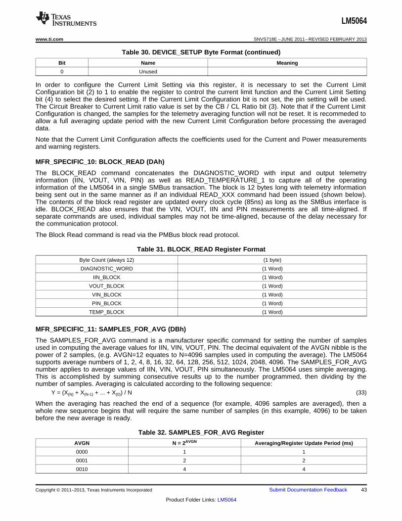
LM5064
www.ti.com SNVS718E –JUNE 2011–REVISED FEBRUARY 2013
Table 30. DEVICE_SETUP Byte Format (continued)
Bit Name Meaning
0 Unused
In order to configure the Current Limit Setting via this register, it is necessary to set the Current LimitConfiguration bit (2) to 1 to enable the register to control the current limit function and the Current Limit Settingbit (4) to select the desired setting. If the Current Limit Configuration bit is not set, the pin setting will be used.The Circuit Breaker to Current Limit ratio value is set by the CB / CL Ratio bit (3). Note that if the Current LimitConfiguration is changed, the samples for the telemetry averaging function will not be reset. It is recommeded toallow a full averaging update period with the new Current Limit Configuration before processing the averageddata.
Note that the Current Limit Configuration affects the coefficients used for the Current and Power measurementsand warning registers.
MFR_SPECIFIC_10: BLOCK_READ (DAh)
The BLOCK_READ command concatenates the DIAGNOSTIC_WORD with input and output telemetryinformation (IIN, VOUT, VIN, PIN) as well as READ_TEMPERATURE_1 to capture all of the operatinginformation of the LM5064 in a single SMBus transaction. The block is 12 bytes long with telemetry informationbeing sent out in the same manner as if an individual READ_XXX command had been issued (shown below).The contents of the block read register are updated every clock cycle (85ns) as long as the SMBus interface isidle. BLOCK_READ also ensures that the VIN, VOUT, IIN and PIN measurements are all time-aligned. Ifseparate commands are used, individual samples may not be time-aligned, because of the delay necessary forthe communication protocol.
The Block Read command is read via the PMBus block read protocol.
Table 31. BLOCK_READ Register Format
Byte Count (always 12) (1 byte)
DIAGNOSTIC_WORD (1 Word)
IIN_BLOCK (1 Word)
VOUT_BLOCK (1 Word)
VIN_BLOCK (1 Word)
PIN_BLOCK (1 Word)
TEMP_BLOCK (1 Word)
MFR_SPECIFIC_11: SAMPLES_FOR_AVG (DBh)
The SAMPLES_FOR_AVG command is a manufacturer specific command for setting the number of samplesused in computing the average values for IIN, VIN, VOUT, PIN. The decimal equivalent of the AVGN nibble is thepower of 2 samples, (e.g. AVGN=12 equates to N=4096 samples used in computing the average). The LM5064supports average numbers of 1, 2, 4, 8, 16, 32, 64, 128, 256, 512, 1024, 2048, 4096. The SAMPLES_FOR_AVGnumber applies to average values of IIN, VIN, VOUT, PIN simultaneously. The LM5064 uses simple averaging.This is accomplished by summing consecutive results up to the number programmed, then dividing by thenumber of samples. Averaging is calculated according to the following sequence:
Y = (X(N) + X(N-1) + ... + X(0)) / N (33)
When the averaging has reached the end of a sequence (for example, 4096 samples are averaged), then awhole new sequence begins that will require the same number of samples (in this example, 4096) to be takenbefore the new average is ready.
Table 32. SAMPLES_FOR_AVG Register
AVGN N = 2AVGN Averaging/Register Update Period (ms)
0000 1 1
0001 2 2
0010 4 4
Copyright © 2011–2013, Texas Instruments Incorporated Submit Documentation Feedback 43
Product Folder Links: LM5064

LM5064
SNVS718E –JUNE 2011–REVISED FEBRUARY 2013 www.ti.com
Table 32. SAMPLES_FOR_AVG Register (continued)
AVGN N = 2AVGN Averaging/Register Update Period (ms)
0011 8 8
0100 16 16
0101 32 32
0110 64 64
0111 128 128
1000 256 256
1001 512 512
1010 1024 1024
1011 2048 2048
1100 4096 4096
Note that a change in the SAMPLES_FOR_AVG register will not be reflected in the average telemetrymeasurements until the present averaging interval has completed. The default setting for AVGN is 0000,therefore, the average telemetry will mirror the instantaneous telemetry until a value higher than zero isprogrammed.
The SAMPLES_FOR_AVG register is accessed via the PMBus read / write byte protocol.
Table 33. SAMPLES_FOR_AVG Register
Value Meaning Default
0h – 0Ch Exponent (AVGN) for number of samples to 00haverage over
MFR_SPECIFIC_12: READ_AVG_VIN (DCh)
The READ_AVG_VIN command will report the 12-bit ADC measured input average voltage. If the data is notready, the returned value will be the previous averaged data. However, if there is no previously averaged data,the default value (0000h) will be returned. This data is read with the PMBus Read Word protocol. This registershould use the coefficients shown in Table 41.
Table 34. READ_AVG_VIN Register
Value Meaning Default
0h – 0FFFh Average of measured values for input 0000hvoltage
MFR_SPECIFIC_13: READ_AVG_VOUT (DDh)
The READ_AVG_VOUT command will report the 12-bit ADC measured OUT pin average voltage. The returnedvalue will be the default value (0000h) or previous data when the average data is not ready. This data is readwith the PMBus Read Word protocol. This register should use the coefficients shown in Table 41.
Table 35. READ_AVG_VOUT Register
Value Meaning Default
0h – 0FFFh Average of measured values for output 0000hvoltage
MFR_SPECIFIC_14: READ_AVG_IIN (DEh)
The READ_AVG_IIN command will report the 12-bit ADC measured VAUXH average voltage. The returnedvalue will be the default value (0000h) or previous data when the average data is not ready. This data is readwith the PMBus Read Word protocol. This register should use the coefficients shown in Table 41.
44 Submit Documentation Feedback Copyright © 2011–2013, Texas Instruments Incorporated
Product Folder Links: LM5064
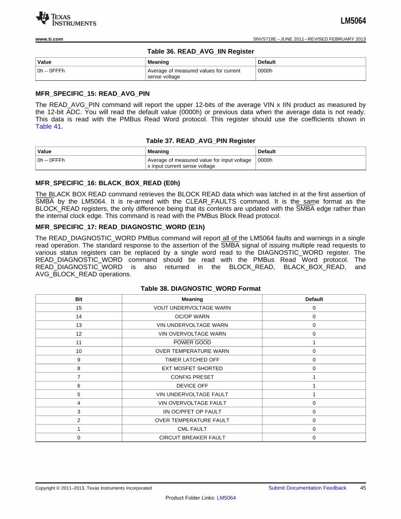
LM5064
www.ti.com SNVS718E –JUNE 2011–REVISED FEBRUARY 2013
Table 36. READ_AVG_IIN Register
Value Meaning Default
0h – 0FFFh Average of measured values for current 0000hsense voltage
MFR_SPECIFIC_15: READ_AVG_PIN
The READ_AVG_PIN command will report the upper 12-bits of the average VIN x IIN product as measured bythe 12-bit ADC. You will read the default value (0000h) or previous data when the average data is not ready.This data is read with the PMBus Read Word protocol. This register should use the coefficients shown inTable 41.
Table 37. READ_AVG_PIN Register
Value Meaning Default
0h – 0FFFh Average of measured value for input voltage 0000hx input current sense voltage
MFR_SPECIFIC_16: BLACK_BOX_READ (E0h)
The BLACK BOX READ command retrieves the BLOCK READ data which was latched in at the first assertion ofSMBA by the LM5064. It is re-armed with the CLEAR_FAULTS command. It is the same format as theBLOCK_READ registers, the only difference being that its contents are updated with the SMBA edge rather thanthe internal clock edge. This command is read with the PMBus Block Read protocol.
MFR_SPECIFIC_17: READ_DIAGNOSTIC_WORD (E1h)
The READ_DIAGNOSTIC_WORD PMBus command will report all of the LM5064 faults and warnings in a singleread operation. The standard response to the assertion of the SMBA signal of issuing multiple read requests tovarious status registers can be replaced by a single word read to the DIAGNOSTIC_WORD register. TheREAD_DIAGNOSTIC_WORD command should be read with the PMBus Read Word protocol. TheREAD_DIAGNOSTIC_WORD is also returned in the BLOCK_READ, BLACK_BOX_READ, andAVG_BLOCK_READ operations.
Table 38. DIAGNOSTIC_WORD Format
Bit Meaning Default
15 VOUT UNDERVOLTAGE WARN 0
14 OC/OP WARN 0
13 VIN UNDERVOLTAGE WARN 0
12 VIN OVERVOLTAGE WARN 0
11 POWER GOOD 1
10 OVER TEMPERATURE WARN 0
9 TIMER LATCHED OFF 0
8 EXT MOSFET SHORTED 0
7 CONFIG PRESET 1
6 DEVICE OFF 1
5 VIN UNDERVOLTAGE FAULT 1
4 VIN OVERVOLTAGE FAULT 0
3 IIN OC/PFET OP FAULT 0
2 OVER TEMPERATURE FAULT 0
1 CML FAULT 0
0 CIRCUIT BREAKER FAULT 0
Copyright © 2011–2013, Texas Instruments Incorporated Submit Documentation Feedback 45
Product Folder Links: LM5064
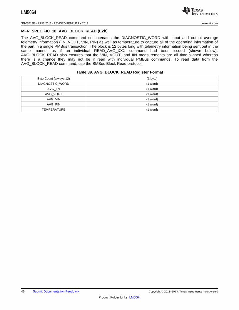
LM5064
SNVS718E –JUNE 2011–REVISED FEBRUARY 2013 www.ti.com
MFR_SPECIFIC_18: AVG_BLOCK_READ (E2h)
The AVG_BLOCK_READ command concatenates the DIAGNOSTIC_WORD with input and output averagetelemetry information (IIN, VOUT, VIN, PIN) as well as temperature to capture all of the operating information ofthe part in a single PMBus transaction. The block is 12 bytes long with telemetry information being sent out in thesame manner as if an individual READ_AVG_XXX command had been issued (shown below).AVG_BLOCK_READ also ensures that the VIN, VOUT, and IIN measurements are all time-aligned whereasthere is a chance they may not be if read with individual PMBus commands. To read data from theAVG_BLOCK_READ command, use the SMBus Block Read protocol.
Table 39. AVG_BLOCK_READ Register Format
Byte Count (always 12) (1 byte)
DIAGNOSTIC_WORD (1 word)
AVG_IIN (1 word)
AVG_VOUT (1 word)
AVG_VIN (1 word)
AVG_PIN (1 word)
TEMPERATURE (1 word)
46 Submit Documentation Feedback Copyright © 2011–2013, Texas Instruments Incorporated
Product Folder Links: LM5064
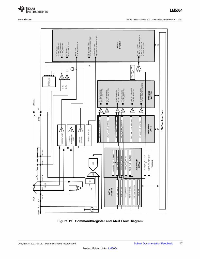
S/ H
MU
XA
DC
VE
E
OU
T
IIN
VA
UX
DIO
DE
RE
AD
_VIN
88h
RE
AD
_IIN
D1h
RE
AD
_PIN
D2h
RE
AD
_ VO
UT
8B
h
TE
MP
ER
AT
UR
E 8
Dh
VA
UX
D0 h
VIN
_UV
_ WA
RN
_LIM
IT 5
8h
VIN
_OV
_ WA
RN
_LIM
IT 5
7hC
MP
CM
PV
IN_ U
V W
AR
NIN
GS
TA
TU
S_I
NP
UT
7C
h
VIN
_OV
WA
RN
ING
ST
AT
US
_ IN
PU
T 7
Ch
IIN_O
C_ W
AR
N_L
IMIT
D3 h
RE
AD
_AV
G_V
IN D
Ch
SA
MP
LES
_FO
R_A
VG
DB
h
RE
AD
_AV
G_V
OU
T D
Dh
RE
AD
_ AV
G_ I
IN D
Eh
RE
AD
_AV
G_P
IN D
FhU
VLO
/EN
OV
LO
SE
NS
E
CM
PIIN
_OC
WA
RN
ING
ST
AT
US
_IN
PU
T 7
Ch
CM
P2.
47V
2.48
V
VIN
OV
FA
ULT
ST
AT
US
_ IN
PU
T 7
Ch
VIN
UV
FA
ULT
ST
AT
US
_IN
PU
T 7
Ch
ST
AT
US
_WO
RD
79h
ST
AT
US
_BY
TE
78h
CU
RR
EN
T L
IMIT
MO
SF
ET
D
ISS
IPA
TIO
N
LIM
IT
CIR
CU
ITB
RE
AK
ER
IIN O
C F
AU
LTS
TA
TU
S_I
NP
UT
7C
h
Circ
uit B
reak
er F
AU
LTS
TA
TU
S_M
FR
_SP
EC
IFIC
80 h
PIN
_ OP
_WA
RN
_LIM
IT D
4hC
MP
PIN
_ OP
WA
RN
ING
ST
AT
US
_ IN
PU
T 7
Ch
VO
UT
_UV
_ WA
RN
_ LIM
IT 4
3 hC
MP
VO
UT
_UV
WA
RN
ING
ST
AT
US
_VO
UT
7A
h
OT
_ WA
RN
ING
_LIM
IT 5
1 hC
MP
OT
_ FA
ULT
_ LIM
IT 4
Fh
CM
PO
T_F
AU
LT_L
IMIT
ST
AT
US
_TE
MP
ER
AT
UR
E 7
Dh
ST
AT
US
_WO
RD
79h
ST
AT
US
_BY
TE
78 h
OT
_WA
RN
ING
_ LIM
ITS
TA
TU
S_T
EM
PE
RA
TU
RE
7D
h
MO
SF
ET
ST
AT
US
FE
T S
hort
ed F
AU
LTS
TA
TU
S_M
FR
_SP
EC
IFIC
80 h
GA
TE
MA
SK
FA
UL
TS
YS
TE
M
WA
RN
ING
SY
ST
EM
DA
TA
O
UT
PU
T
WA
RN
ING
LIM
ITS
AV
ER
AG
ED
D
AT
A
RE
AD
_PIN
_ PE
AK
D5h
CLE
AR
_ PIN
_ PE
AK
D6 h
PE
AK
-HO
LD
-48
To
Load
PM
Bu
s In
terf
ace
CM
P
CM
P
CM
P
CM
P
-+
GA
TE
-48V
VE
E_K
SE
NS
E_K
VA
UX
H
LM5064
www.ti.com SNVS718E –JUNE 2011–REVISED FEBRUARY 2013
Figure 19. Command/Register and Alert Flow Diagram
Copyright © 2011–2013, Texas Instruments Incorporated Submit Documentation Feedback 47
Product Folder Links: LM5064

X =1m
(Y x 10-R - b)
LM5064
SNVS718E –JUNE 2011–REVISED FEBRUARY 2013 www.ti.com
READING AND WRITING TELEMETRY DATA AND WARNING THRESHOLDS
All measured telemetry data and user programmed warning thresholds are communicated in 12-bit two’scompliment binary numbers read/written in 2 byte increments conforming to the Direct format as described insection 8.3.3 of the PMBus Power System Management Protocol Specification 1.1 (Part II). The organization ofthe bits in the telemetry or warning word is shown in Table 40, where Bit_11 is the most significant bit (MSB) andBit_0 is the least significant bit (LSB). The decimal equivalent of all warning and telemetry words are constrainedto be within the range of 0 to 4095, with the exception of temperature. The decimal equivalent value of thetemperature word ranges from 0 to 65535.
Table 40. Telemetry and Warning Word Format
Byte B7 B6 B5 B4 B3 B2 B1 B0
1 Bit_7 Bit_6 Bit_5 Bit_4 Bit_3 Bit_2 Bit_1 Bit_0
2 0 0 0 0 Bit_11 Bit_10 Bit_9 Bit_8
Conversion from direct format to real-world dimensions of current, voltage, power, and temperature isaccomplished by determining appropriate coefficients as described in section 7.2.1 of the PMBus Power SystemManagement Protocol Specification 1.1 (Part II). According to this specification, the host system converts thevalues received into a reading of volts, amperes, watts, or other units using the following relationship:
(34)
Where:
X: the calculated "real-world" value (volts, amps, watt, etc.)
m: the slope coefficient
Y: a two byte two's complement integer received from device
b: the offset, a two byte, two's complement integer
R: the exponent, a one byte two's complement integer
R is only necessary in systems where m is required to be an integer (for example, where m may be stored in aregister in an integrated circuit). In those cases, R only needs to be large enough to yield the desired accuracy.
Table 41. Telemetry and Warning Conversion Coefficients
Commands Condition Format Number of m b R UnitsData Bytes
READ_VIN, READ_AVG_VIN DIRECT 2 4611 -642 -2 VVIN_OV_WARN_LIMITVIN_UV_WARN_LIMIT
READ_VOUT, READ_AVG_VOUT DIRECT 2 4621 423 -2 VVOUT_UV_WARN_LIMIT
READ_VAUX DIRECT 2 13808 0 -1 V(1)READ_IIN, READ_AVG_IIN CL = VDD DIRECT 2 10742 1552 -2 AMFR_IIN_OC_WARN_LIMIT(1)READ_IN, READ_AVG_IN CL = VEE DIRECT 2 5456 2118 -2 AMFR_IIN_OC_WARN_LIMIT
(1)READ_PIN, READ_AVG_PIN, CL = VDD DIRECT 2 1204 8524 -3 WREAD_PIN_PEAK
MFR_PIN_OP_WARN_LIMIT(1)READ_PIN, READ_AVG_PIN, CL = VEE DIRECT 2 612 11202 -3 W
READ_PIN_PEAKMFR_PIN_OP_WARN_LIMIT
READ_TEMPERATURE_1 DIRECT 2 16000 0 -3 °COT_WARN_LIMITOT_FAULT_LIMIT
(1) The coefficients relating to current/power measurements and warning thresholds shown are normalized to a sense resistor (RS) value of1 mΩ. In general, the current/power coefficients can be calculated using the relationships shown in Table 42.
48 Submit Documentation Feedback Copyright © 2011–2013, Texas Instruments Incorporated
Product Folder Links: LM5064
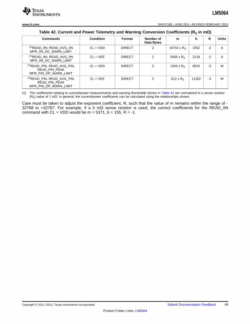
LM5064
www.ti.com SNVS718E –JUNE 2011–REVISED FEBRUARY 2013
Table 42. Current and Power Telemetry and Warning Conversion Coefficients (RS in mΩ)
Commands Condition Format Number of m b R UnitsData Bytes
(1)READ_IIN, READ_AVG_IIN CL = VDD DIRECT 2 10742 x RS 1552 -2 AMFR_IIN_OC_WARN_LIMIT
(1)READ_IIN, READ_AVG_IIN CL = VEE DIRECT 2 5456 x RS 2118 -2 AMFR_IIN_OC_WARN_LIMIT
(1)READ_PIN, READ_AVG_PIN, CL = VDD DIRECT 2 1204 x RS 8524 -3 WREAD_PIN_PEAK
MFR_PIN_OP_WARN_LIMIT(1)READ_PIN, READ_AVG_PIN, CL = VEE DIRECT 2 612 x RS 11202 -3 W
READ_PIN_PEAKMFR_PIN_OP_WARN_LIMIT
(1) The coefficients relating to current/power measurements and warning thresholds shown in Table 41 are normalized to a sense resistor(RS) value of 1 mΩ. In general, the current/power coefficients can be calculated using the relationships shown.
Care must be taken to adjust the exponent coefficient, R, such that the value of m remains within the range of -32768 to +32767. For example, if a 5 mΩ sense resistor is used, the correct coefficients for the READ_IINcommand with CL = VDD would be m = 5371, b = 155, R = -1.
Copyright © 2011–2013, Texas Instruments Incorporated Submit Documentation Feedback 49
Product Folder Links: LM5064
X =1m
(Y x 10-R - b)
LM5064
SNVS718E –JUNE 2011–REVISED FEBRUARY 2013 www.ti.com
DETERMINING TELEMETRY COEFFICIENTS EMPIRICALLY WITH LINEAR FIT
The coefficients for telemetry measurements and warning thresholds presented in Table 41 are adequate for themajority of applications. Current and power coefficients must be calculated per application as they are dependenton the value of the sense resistor, RS, used. Table 42 provides the equations necessary for calculating thecurrent and power coefficients for the general case. The small signal nature of the current measurement make itand the power measurement more susceptible to PCB parasitics than other telemetry channels. This may causeslight variations in the optimum coefficients (m, b, R) for converting from Direct format digital values to real-worldvalues (for example, Amps and Watts). The optimum coefficients can be determined empirically for a specificapplication and PCB layout using two or more measurements of the telemetry channel of interest. The currentcoefficients can be determined using the following method:1. While the LM5064 is in normal operation measure the voltage across the sense resistor using kelvin test
points and a high accuracy DVM while controlling the load current. Record the integer value returned by theREAD_AVG_IIN command (with the SAMPLES_FOR_AVG set to a value greater than 0) for two or morevoltages across the sense resistor. For best results, the individual READ_AVG_IIN measurements shouldspan nearly the full scale range of the current (For example, voltage across RS of 5 mV and 20 mV).
2. Convert the measured voltages to currents by dividing them by the value of RS. For best accuracy the valueof RS should be measured. Table 43 assumes a sense resistor value of 5mΩ.
Table 43. Measurements for linear fit determination of current coefficients:
Measured voltage across Measured Current (A) READ_AVG_IINRS (V) (integer value)
0.005 1 568
0.01 2 1108
0.02 4 2185
1. Using the spreadsheet or math program of your choice determine the slope and the y-intercept of the datareturned by the READ_AVG_IIN command versus the measured current. For the data shown in Table 42:– READ_AVG_IN value = slope x (Measured Current) + (y-intercept)– slope = 538.9– y-intercept = 29.5
2. To determine the ‘m’ coefficient, simply shift the decimal point of the calculated slope to arrive at an integerwith a suitable number of significant digits for accuracy (typically 4) while staying with the range of -32768 to+32767. This shift in the decimal point equates to the ‘R’ coefficient. For the slope value shown above, thedecimal point would be shifted to the right once hence R = -1.
3. Once the ‘R’ coefficient has been determined, the ‘b’ coefficient is found by multiplying the y-intercept by10-R. In this case the value of b = 295.– Calculated Current Coefficients:– m = 5389– b = 295– R = -1
(35)
Where:
X: the calculated "real-world" value (volts, amps, watts, temperature)
m: the slope coefficient, is the two byte, two's complement integer
Y: a two byte two's complement integer received from device
b: the offset, a two byte, two's complement integer
R: the exponent, a one byte two's complement integer
The above procedure can be repeated to determine the coefficients of any telemetry channel simply bysubstituting measured current for some other parameter (for example, power, voltage, etc.).
50 Submit Documentation Feedback Copyright © 2011–2013, Texas Instruments Incorporated
Product Folder Links: LM5064
LM5064
www.ti.com SNVS718E –JUNE 2011–REVISED FEBRUARY 2013
WRITING TELEMETRY DATA
There are several locations that will require writing data if their optional usage is desired. Use the samecoefficients previously calculated for your application, and apply them using this method as prescribed by thePMBus revision section 7.2.2 "Sending a Value"
Y = (mX + b) x 10R (36)
Where:
X: the calculated "real-world" value (volts, amps, watts, temperature)
m: the slope coefficient, is the two byte, two's complement integer
Y: a two byte two's complement integer received from device
b: the offset, a two byte, two's complement integer
R: the exponent, a one byte two's complement integer
Copyright © 2011–2013, Texas Instruments Incorporated Submit Documentation Feedback 51
Product Folder Links: LM5064
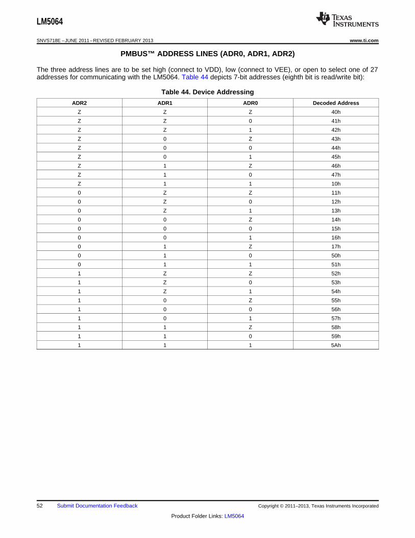
LM5064
SNVS718E –JUNE 2011–REVISED FEBRUARY 2013 www.ti.com
PMBUS™ ADDRESS LINES (ADR0, ADR1, ADR2)
The three address lines are to be set high (connect to VDD), low (connect to VEE), or open to select one of 27addresses for communicating with the LM5064. Table 44 depicts 7-bit addresses (eighth bit is read/write bit):
Table 44. Device Addressing
ADR2 ADR1 ADR0 Decoded Address
Z Z Z 40h
Z Z 0 41h
Z Z 1 42h
Z 0 Z 43h
Z 0 0 44h
Z 0 1 45h
Z 1 Z 46h
Z 1 0 47h
Z 1 1 10h
0 Z Z 11h
0 Z 0 12h
0 Z 1 13h
0 0 Z 14h
0 0 0 15h
0 0 1 16h
0 1 Z 17h
0 1 0 50h
0 1 1 51h
1 Z Z 52h
1 Z 0 53h
1 Z 1 54h
1 0 Z 55h
1 0 0 56h
1 0 1 57h
1 1 Z 58h
1 1 0 59h
1 1 1 5Ah
52 Submit Documentation Feedback Copyright © 2011–2013, Texas Instruments Incorporated
Product Folder Links: LM5064

SCLVIH
VIL
VIH
VIL
P S S P
SDAtHD;DAT
tSU;STO
tHD;STA
tSU;STA
tSU;DAT
tHIGH
tBUF
tLOW
tR tF
LM5064
www.ti.com SNVS718E –JUNE 2011–REVISED FEBRUARY 2013
SMBUS COMMUNICATIONS TIMING REQUIREMENTS
Figure 20. SMBus Timing Diagram
Table 45. SMBus Timing Definition
Symbol Parameter Limits Units Comments
Min Max
FSMB SMBus Operating Frequency 10 400 kHz
TBUF Bus free time between Stop and Start Condition 1.3 µs
THD:STA Hold time after (Repeated) Start Condition. After this 0.6 µsperiod, the first clock is generated.
TSU:STA Repeated Start Condition setup time 0.6 µs
TSU:STO Stop Condition setup time 0.6 µs
THD:DAT Data hold time 85 ns
TSU:DAT Data setup time 100 ns
TTIMEOUT Clock low time-out 25 35 ms (1)
TLOW Clock low period 1.5 µs
THIGH Clock high period 0.6 µs (2)
TLOW:SEXT Cumulative clock low extend time (slave device) 25 ms (3)
TLOW:MEXT Cumulative low extend time (master device) 10 ms (4)
TF Clock or Data Fall Time 20 300 ns (5)
TR Clock or Data Rise Time 20 300 ns (5)
(1) Devices participating in a transfer will timeout when any clock low exceeds the value of TTIMEOUT,MIN of 25 ms. Devices that havedetected a timeout condition must reset the communication no later than TTIMEOUT,MAX of 35 ms. The maximum value must be adheredto by both a master and a slave as it incorporates the cumulative stretch limit for both a master (10ms) and a slave (25ms).
(2) THIGH MAX provides a simple method for devices to detect bus idle conditions.(3) TLOW:SEXT is the cumulative time a slave device is allowed to extend the clock cycles in one message from the initial start to the stop. If
a slave exceeds this time, it is expected to release both its clock and data lines and reset itself.(4) TLOW:MEXT is the cumulative time a master device is allowed to extend its clock cycles within each byte of a message as defined from
start-to-ack, ack-to-ack, or ack-to-stop.(5) Rise and fall time is defined as follows:• TR = ( VILMAX – 0.15) to (VIHMIN + 0.15)• TF = 0.9 VDD to (VILMAX – 0.15)
Copyright © 2011–2013, Texas Instruments Incorporated Submit Documentation Feedback 53
Product Folder Links: LM5064

Alert Mask D8h
From PMBus
From other fault inputs
ARA Auto MaskSet
Clear
Fault Condition
ARA Operation Flag Succeeded
Clear_Fault Command Received
SMBA
LM5064
SNVS718E –JUNE 2011–REVISED FEBRUARY 2013 www.ti.com
SMBA RESPONSE
The SMBA effectively has two masks:
1. The Alert Mask Register at D8h, and
2. The ARA Automatic Mask.
The ARA Automatic Mask is a mask that is set in response to a successful ARA read. An ARA read operationreturns the PMBus address of the lowest addressed part on the bus that has its SMBA asserted. A successfulARA read means that THIS part was the one that returned its address. When a part responds to the ARA read, itreleases the SMBA signal. When the last part on the bus that has an SMBA set has successfully reported itsaddress, the SMBA signal will de-assert.
The way that the LM5064 releases the SMBA signal is by setting the ARA Automatic mask bit for all faultconditions present at the time of the ARA read. All status registers will still show the fault condition, but it will notgenerate and SMBA on that fault again until the ARA Automatic mask is cleared by the host issuing aCLEAR_FAULTS command to this part. This should be done as a routine part of servicing an SMBA condition ona part, even if the ARA read is not done. Figure 21 depicts a schematic version of this flow.
Figure 21. Typical Flow Schematic for SMBA Fault
54 Submit Documentation Feedback Copyright © 2011–2013, Texas Instruments Incorporated
Product Folder Links: LM5064
LM5064
www.ti.com SNVS718E –JUNE 2011–REVISED FEBRUARY 2013
REVISION HISTORY
Changes from Revision D (February 2013) to Revision E Page
• Changed layout of National Data Sheet to TI format .......................................................................................................... 54
Copyright © 2011–2013, Texas Instruments Incorporated Submit Documentation Feedback 55
Product Folder Links: LM5064
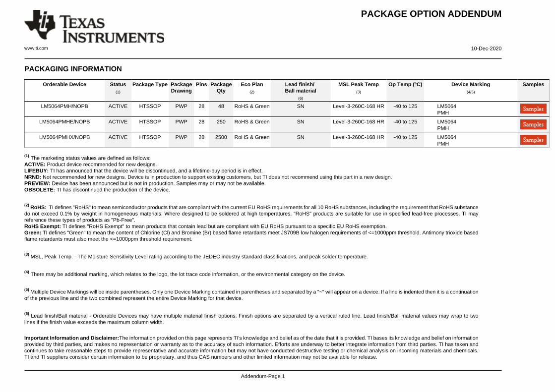
PACKAGE OPTION ADDENDUM
www.ti.com 10-Dec-2020
Addendum-Page 1
PACKAGING INFORMATION
Orderable Device Status(1)
Package Type PackageDrawing
Pins PackageQty
Eco Plan(2)
Lead finish/Ball material
(6)
MSL Peak Temp(3)
Op Temp (°C) Device Marking(4/5)
Samples
LM5064PMH/NOPB ACTIVE HTSSOP PWP 28 48 RoHS & Green SN Level-3-260C-168 HR -40 to 125 LM5064PMH
LM5064PMHE/NOPB ACTIVE HTSSOP PWP 28 250 RoHS & Green SN Level-3-260C-168 HR -40 to 125 LM5064PMH
LM5064PMHX/NOPB ACTIVE HTSSOP PWP 28 2500 RoHS & Green SN Level-3-260C-168 HR -40 to 125 LM5064PMH
(1) The marketing status values are defined as follows:ACTIVE: Product device recommended for new designs.LIFEBUY: TI has announced that the device will be discontinued, and a lifetime-buy period is in effect.NRND: Not recommended for new designs. Device is in production to support existing customers, but TI does not recommend using this part in a new design.PREVIEW: Device has been announced but is not in production. Samples may or may not be available.OBSOLETE: TI has discontinued the production of the device.
(2) RoHS: TI defines "RoHS" to mean semiconductor products that are compliant with the current EU RoHS requirements for all 10 RoHS substances, including the requirement that RoHS substancedo not exceed 0.1% by weight in homogeneous materials. Where designed to be soldered at high temperatures, "RoHS" products are suitable for use in specified lead-free processes. TI mayreference these types of products as "Pb-Free".RoHS Exempt: TI defines "RoHS Exempt" to mean products that contain lead but are compliant with EU RoHS pursuant to a specific EU RoHS exemption.Green: TI defines "Green" to mean the content of Chlorine (Cl) and Bromine (Br) based flame retardants meet JS709B low halogen requirements of <=1000ppm threshold. Antimony trioxide basedflame retardants must also meet the <=1000ppm threshold requirement.
(3) MSL, Peak Temp. - The Moisture Sensitivity Level rating according to the JEDEC industry standard classifications, and peak solder temperature.
(4) There may be additional marking, which relates to the logo, the lot trace code information, or the environmental category on the device.
(5) Multiple Device Markings will be inside parentheses. Only one Device Marking contained in parentheses and separated by a "~" will appear on a device. If a line is indented then it is a continuationof the previous line and the two combined represent the entire Device Marking for that device.
(6) Lead finish/Ball material - Orderable Devices may have multiple material finish options. Finish options are separated by a vertical ruled line. Lead finish/Ball material values may wrap to twolines if the finish value exceeds the maximum column width.
Important Information and Disclaimer:The information provided on this page represents TI's knowledge and belief as of the date that it is provided. TI bases its knowledge and belief on informationprovided by third parties, and makes no representation or warranty as to the accuracy of such information. Efforts are underway to better integrate information from third parties. TI has taken andcontinues to take reasonable steps to provide representative and accurate information but may not have conducted destructive testing or chemical analysis on incoming materials and chemicals.TI and TI suppliers consider certain information to be proprietary, and thus CAS numbers and other limited information may not be available for release.

PACKAGE OPTION ADDENDUM
www.ti.com 10-Dec-2020
Addendum-Page 2
In no event shall TI's liability arising out of such information exceed the total purchase price of the TI part(s) at issue in this document sold by TI to Customer on an annual basis.

TAPE AND REEL INFORMATION
*All dimensions are nominal
Device PackageType
PackageDrawing
Pins SPQ ReelDiameter
(mm)
ReelWidth
W1 (mm)
A0(mm)
B0(mm)
K0(mm)
P1(mm)
W(mm)
Pin1Quadrant
LM5064PMHE/NOPB HTSSOP PWP 28 250 178.0 16.4 6.8 10.2 1.6 8.0 16.0 Q1
LM5064PMHX/NOPB HTSSOP PWP 28 2500 330.0 16.4 6.8 10.2 1.6 8.0 16.0 Q1
PACKAGE MATERIALS INFORMATION
www.ti.com 21-Oct-2021
Pack Materials-Page 1

*All dimensions are nominal
Device Package Type Package Drawing Pins SPQ Length (mm) Width (mm) Height (mm)
LM5064PMHE/NOPB HTSSOP PWP 28 250 208.0 191.0 35.0
LM5064PMHX/NOPB HTSSOP PWP 28 2500 853.0 449.0 35.0
PACKAGE MATERIALS INFORMATION
www.ti.com 21-Oct-2021
Pack Materials-Page 2

www.ti.com
PACKAGE OUTLINE
C
TYP6.66.2
1.1 MAX
26X 0.65
28X 0.300.19
2X8.45
TYP0.200.09
0 - 80.100.02
5.655.25
3.152.75
(1)
0.25GAGE PLANE
0.70.5
A
NOTE 3
9.89.6
BNOTE 4
4.54.3
4214870/A 10/2014
PowerPAD - 1.1 mm max heightPWP0028APLASTIC SMALL OUTLINE
NOTES: 1. All linear dimensions are in millimeters. Any dimensions in parenthesis are for reference only. Dimensioning and tolerancing per ASME Y14.5M. 2. This drawing is subject to change without notice. 3. This dimension does not include mold flash, protrusions, or gate burrs. Mold flash, protrusions, or gate burrs shall not exceed 0.15 mm, per side. 4. This dimension does not include interlead flash. Interlead flash shall not exceed 0.25 mm, per side.5. Reference JEDEC registration MO-153, variation AET.
PowerPAD is a trademark of Texas Instruments.
TM
128
0.1 C A B
1514
PIN 1 IDAREA
SEATING PLANE
0.1 C
SEE DETAIL A
DETAIL ATYPICAL
SCALE 1.800
THERMALPAD

www.ti.com
EXAMPLE BOARD LAYOUT
0.05 MAXALL AROUND
0.05 MINALL AROUND
28X (1.3)
(6.1)
28X (0.45)
(0.9) TYP
28X (1.5)
28X (0.45)
26X(0.65)
(3)
(3.4)NOTE 9
(5.5)SOLDER
MASKOPENING
(9.7)
(1.3)
(1.3) TYP
(5.8)
( ) TYPVIA
0.2
(0.65) TYP
4214870/A 10/2014
PowerPAD - 1.1 mm max heightPWP0028APLASTIC SMALL OUTLINE
SOLDER MASKDEFINED PAD
LAND PATTERN EXAMPLESCALE:6X
HV / ISOLATION OPTION0.9 CLEARANCE CREEPAGE
OTHER DIMENSIONS IDENTICAL TO IPC-7351
TM
NOTES: (continued) 6. Publication IPC-7351 may have alternate designs. 7. Solder mask tolerances between and around signal pads can vary based on board fabrication site. 8. This package is designed to be soldered to a thermal pad on the board. For more information, see Texas Instruments literature numbers SLMA002 (www.ti.com/lit/slma002) and SLMA004 (www.ti.com/lit/slma004).9. Size of metal pad may vary due to creepage requirement.
METALSOLDER MASKOPENING
NON SOLDER MASKDEFINED
SOLDER MASK DETAILS
SOLDER MASKOPENING
METAL UNDERSOLDER MASK
SOLDER MASKDEFINED
SYMM
SYMM
SEE DETAILS
1
14 15
28
METAL COVEREDBY SOLDER MASK
SOLDERMASK
OPENING
IPC-7351 NOMINAL0.65 CLEARANCE CREEPAGE

www.ti.com
EXAMPLE STENCIL DESIGN
28X (1.3)
28X (0.45)
(6.1)
28X (1.5)
28X (0.45)
26X (0.65)
(3)
(5.5)BASED ON
0.127 THICKSTENCIL
(5.8)
4214870/A 10/2014
PowerPAD - 1.1 mm max heightPWP0028APLASTIC SMALL OUTLINE
2.66 X 4.770.1782.88 X 5.160.152
3.0 X 5.5 (SHOWN)0.1273.55 X 6.370.1
SOLDER STENCILOPENING
STENCILTHICKNESS
SEE TABLE FORDIFFERENT OPENINGSFOR OTHER STENCILTHICKNESSES
NOTES: (continued) 10. Laser cutting apertures with trapezoidal walls and rounded corners may offer better paste release. IPC-7525 may have alternate design recommendations. 11. Board assembly site may have different recommendations for stencil design.
TM
SOLDER PASTE EXAMPLEEXPOSED PAD
100% PRINTED SOLDER COVERAGE AREASCALE:6X
HV / ISOLATION OPTION0.9 CLEARANCE CREEPAGE
OTHER DIMENSIONS IDENTICAL TO IPC-7351
SYMM
SYMM
1
14 15
28
BASED ON0.127 THICK
STENCIL BY SOLDER MASKMETAL COVERED
IPC-7351 NOMINAL0.65 CLEARANCE CREEPAGE
IMPORTANT NOTICE AND DISCLAIMERTI PROVIDES TECHNICAL AND RELIABILITY DATA (INCLUDING DATA SHEETS), DESIGN RESOURCES (INCLUDING REFERENCE DESIGNS), APPLICATION OR OTHER DESIGN ADVICE, WEB TOOLS, SAFETY INFORMATION, AND OTHER RESOURCES “AS IS” AND WITH ALL FAULTS, AND DISCLAIMS ALL WARRANTIES, EXPRESS AND IMPLIED, INCLUDING WITHOUT LIMITATION ANY IMPLIED WARRANTIES OF MERCHANTABILITY, FITNESS FOR A PARTICULAR PURPOSE OR NON-INFRINGEMENT OF THIRD PARTY INTELLECTUAL PROPERTY RIGHTS.These resources are intended for skilled developers designing with TI products. You are solely responsible for (1) selecting the appropriate TI products for your application, (2) designing, validating and testing your application, and (3) ensuring your application meets applicable standards, and any other safety, security, regulatory or other requirements.These resources are subject to change without notice. TI grants you permission to use these resources only for development of an application that uses the TI products described in the resource. Other reproduction and display of these resources is prohibited. No license is granted to any other TI intellectual property right or to any third party intellectual property right. TI disclaims responsibility for, and you will fully indemnify TI and its representatives against, any claims, damages, costs, losses, and liabilities arising out of your use of these resources.TI’s products are provided subject to TI’s Terms of Sale or other applicable terms available either on ti.com or provided in conjunction with such TI products. TI’s provision of these resources does not expand or otherwise alter TI’s applicable warranties or warranty disclaimers for TI products.TI objects to and rejects any additional or different terms you may have proposed. IMPORTANT NOTICE
Mailing Address: Texas Instruments, Post Office Box 655303, Dallas, Texas 75265Copyright © 2021, Texas Instruments Incorporated


![A Review on Impacts of Power Quality, Control and .... The negative aspects of this technology are ... The main causes of voltage swells are a voltage regulator [16]. In literature](https://img.dokumen.tips/doc/110x75/5ea5e93620a75a5fe31ebf7b/a-review-on-impacts-of-power-quality-control-and-the-negative-aspects-of.jpg)