Embed Size (px)
Citation preview
Product
Folder
Sample &Buy
Technical
Documents
Tools &
Software
Support &Community
LM321SNOS935C –FEBRUARY 2001–REVISED DECEMBER 2014
LM321 Low Power Single Operational Amplifier1 Features 3 Description
The LM321 brings performance and economy to low1• (VCC = 5 V, TA = 25°C. Typical values unless
power systems. With a high unity gain frequency andspecified.)a specified 0.4-V/µs slew rate, the quiescent current
• Gain-Bandwidth Product 1 MHz is only 430-µA/amplifier (5 V). The input common• Low Supply Current 430 µA mode range includes ground and therefore the device
is able to operate in single supply applications as well• Low Input Bias Current 45 nAas in dual supply applications. It is also capable of• Wide Supply Voltage Range 3 V to 32 V comfortably driving large capacitive loads.
• Stable With High Capacitive LoadsThe LM321 is available in the SOT-23 package.• Single Version of LM324 Overall the LM321 is a low power, wide supply rangeperformance operational amplifier that can be2 Applications designed into a wide range of applications at aneconomical price without sacrificing valuable board• Chargersspace.• Power Supplies
• Industrial: Controls, Instruments Device Information(1)
• Desktops PART NUMBER PACKAGE BODY SIZE (NOM)• Communications Infrastructure LM321 SOT (5) 2.90 mm × 1.60 mm
(1) For all available packages, see the orderable addendum atthe end of the datasheet.
Simplified Schematic
1
An IMPORTANT NOTICE at the end of this data sheet addresses availability, warranty, changes, use in safety-critical applications,intellectual property matters and other important disclaimers. PRODUCTION DATA.
LM321SNOS935C –FEBRUARY 2001–REVISED DECEMBER 2014 www.ti.com
Table of Contents7.3 Feature Description................................................... 71 Features .................................................................. 17.4 Device Functional Modes.......................................... 82 Applications ........................................................... 1
8 Application and Implementation .......................... 93 Description ............................................................. 18.1 Application Information.............................................. 94 Revision History..................................................... 28.2 Typical Applications ................................................ 105 Pin Configuration and Functions ......................... 3
9 Power Supply Recommendations ...................... 136 Specifications......................................................... 310 Layout................................................................... 136.1 Absolute Maximum Ratings ..................................... 3
10.1 Layout Guidelines ................................................. 136.2 ESD Ratings.............................................................. 310.2 Layout Example .................................................... 146.3 Recommended Operating Conditions....................... 4
11 Device and Documentation Support ................. 156.4 Thermal Information .................................................. 411.1 Trademarks ........................................................... 156.5 Electrical Characteristics........................................... 411.2 Electrostatic Discharge Caution............................ 156.6 Typical Characteristics .............................................. 611.3 Glossary ................................................................ 157 Detailed Description .............................................. 7
12 Mechanical, Packaging, and Orderable7.1 Overview ................................................................... 7Information ........................................................... 157.2 Functional Block Diagram ......................................... 7
4 Revision HistoryNOTE: Page numbers for previous revisions may differ from page numbers in the current version.
Changes from Revision B (March 2013) to Revision C Page
• Added Pin Configuration and Functions section, ESD Ratings table, Feature Description section, Device FunctionalModes, Application and Implementation section, Power Supply Recommendations section, Layout section, Deviceand Documentation Support section, and Mechanical, Packaging, and Orderable Information section .............................. 1
Changes from Revision A (March 2013) to Revision B Page
• Changed layout of National Data Sheet to TI format ........................................................................................................... 13
2 Submit Documentation Feedback Copyright © 2001–2014, Texas Instruments Incorporated
Product Folder Links: LM321

LM321www.ti.com SNOS935C –FEBRUARY 2001–REVISED DECEMBER 2014
5 Pin Configuration and Functions
DBV Package5-Pin SOT-23
Top View
Pin FunctionsPIN
I/O DESCRIPTIONNAME NO.+IN 1 I Noninverting inputV– 2 — Negative (lowest) power supply–IN 3 I Inverting inputOUTPUT 4 O OutputV+ 5 — Positive (highest) power supply
6 Specifications
6.1 Absolute Maximum Ratings (1)
MIN MAX UNITDifferential Input Voltage ±Supply VoltageInput Current (VIN < −0.3 V) (2) 50 mASupply Voltage (V+ - V−) 32 VInput Voltage −0.3 32 VOutput Short Circuit to GND, V+ ≤ 15 V and TA = 25°C (3) ContinuousJunction Temperature (4) 150 °C
Mounting Temperature: Lead temperature (Soldering, 10 sec) 260 °CMounting Temperature: Infrared (10 sec) 215 °C
Storage temperature, Tstg –65 150 °C
(1) Stresses beyond those listed under Absolute Maximum Ratings may cause permanent damage to the device. These are stress ratingsonly, which do not imply functional operation of the device at these or any other conditions beyond those indicated under RecommendedOperating Conditions. Exposure to absolute-maximum-rated conditions for extended periods may affect device reliability.
(2) This input current will only exist when the voltage at any of the input leads is driven negative. It is due to the collector base junction ofthe input PNP transistors becoming forward biased and thereby acting as input diode clamps. In addition to this diode action, there isalso lateral NPN parasitic transistor action on the IC chip. This transistor action can cause the output voltages of the operational ampliferto go to the V+ voltage level (or to ground for a large overdrive) for the time duration that an input is driven negative. This is notdestructive and normal output states will re-establish when the input voltage, which was negative, again returns to a value greater than−0.36V (at 25°C).
(3) Short circuits from the output V+ can cause excessive heating and eventual destruction. When considering short circuits to ground themaximum output current is approximately 40mA independent of the magnitude of V+. At values of supply voltage in excess of +15V,continuous short circuits can exceed the power dissipation ratings and cause eventual destruction.
(4) The maximum power dissipation is a function of TJ(MAX), θJA , and TA. The maximum allowable power dissipation at any ambienttemperature is PD = (TJ(MAX) - TA)/ θJA. All numbers apply for packages soldered directly onto a PC board.
6.2 ESD RatingsVALUE UNIT
V(ESD) Electrostatic discharge Human-body model (HBM), per ANSI/ESDA/JEDEC JS-001 (1) ±300 V
(1) JEDEC document JEP155 states that 500-V HBM allows safe manufacturing with a standard ESD control process.
Copyright © 2001–2014, Texas Instruments Incorporated Submit Documentation Feedback 3
Product Folder Links: LM321

LM321SNOS935C –FEBRUARY 2001–REVISED DECEMBER 2014 www.ti.com
6.3 Recommended Operating ConditionsMIN MAX UNIT
Temperature Range −40 85 °CSupply Voltage 3 30 V
6.4 Thermal InformationLM321
THERMAL METRIC (1) DBV UNIT5 PINS
RθJA Junction-to-ambient thermal resistance 265 °C/W
(1) For more information about traditional and new thermal metrics, see the IC Package Thermal Metrics application report, SPRA953.
6.5 Electrical CharacteristicsUnless otherwise specified, all limits specified for at TA = 25°C; V+ = 5 V, V− = 0 V, VO = 1.4 V
PARAMETER TEST CONDITIONS MIN TYP MAX UNITVOS Input Offset Voltage (1)2 7
mV(1), –40°C ≤ TJ ≤ 85°C 9IOS Input Offset Current 5 50
nA–40°C ≤ TJ ≤ 85°C 150
IB Input Bias Current (2) 45 250nA
–40°C ≤ TJ ≤ 85°C 500VCM Input Common-Mode Voltage V+ = 30 V (3), for CMRR > = 50dB 0 V+ - 1.5
Range VV+ = 30 V (3), for CMRR > = 50dB, –40°C ≤ V+ - 2TJ ≤ 85°C
AV Large Signal Voltage Gain (V+ = 15 V, RL = 2kΩ, VO = 1.4 V to 11.4 25 100V)
V/mV(V+ = 15 V, RL = 2kΩ, VO = 1.4 V to 11.4 15V), –40°C ≤ TJ ≤ 85°C
PSRR Power Supply Rejection Ratio RS ≤ 10kΩ, 65 100 dBV+ ≤ 5 V to 30 VCMRR Common Mode Rejection RS ≤ 10kΩ 65 85 dBRatioVO Output Swing VOH V+ = 30 V, RL = 2kΩ, –40°C ≤ TJ ≤ 85°C 26
VV+ = 30 V, RL = 10kΩ, –40°C ≤ TJ ≤ 85°C 27 28
VOL V+ = 5 V, RL = 10kΩ, –40°C ≤ TJ ≤ 85°C 5 20 mVIS Supply Current, No Load V+ = 5 V 0.430 1.15
V+ = 5 V, –40°C ≤ TJ ≤ 85°C 0.7 1.2mA
V+ = 30 V 0.660 2.85V+ = 30 V, –40°C ≤ TJ ≤ 85°C 1.5 3
ISOURCE Output Current Sourcing VID = +1 V, V+ = 15 V, VO = 2 V 20 40mAVID = +1 V, V+ = 15 V, VO = 2 V, –40°C ≤ 10 20
TJ ≤ 85°CISINK Output Current Sinking VID = −1 V, V+ = 15 V, VO = 2 V 10 20
mAVID = −1 V, V+ = 15 V, VO = 2 V, –40°C ≤TJ ≤ 85°C 5 8VID = −1 V, V+ = 15 V, VO = 0.2 V 12 100 µA
(1) VO ≅ 1.4 V, RS = 0Ω with V+ from 5 V to 30 V; and over the full input common-mode range (0 V to V+ - 1.5 V) at 25°C.(2) The direction of the input current is out of the IC due to the PNP input stage. This current is essentially constant, independent of the
state of the output so no loading change exists on the input lines.(3) The input common-mode voltage of either input signal voltage should not be allowed to go negative by more than 0.3 V (at 25°C). The
upper end of the common-mode voltage range is V+ - 1.5 V at 25°C, but either or both inputs can go to +32 V without damage,independent of the magnitude of V+.
4 Submit Documentation Feedback Copyright © 2001–2014, Texas Instruments Incorporated
Product Folder Links: LM321

LM321www.ti.com SNOS935C –FEBRUARY 2001–REVISED DECEMBER 2014
Electrical Characteristics (continued)Unless otherwise specified, all limits specified for at TA = 25°C; V+ = 5 V, V− = 0 V, VO = 1.4 V
PARAMETER TEST CONDITIONS MIN TYP MAX UNITIO Output Short Circuit to Ground V+ = 15 V 40 85 mA(4)
SR Slew Rate V+ = 15 V, RL = 2kΩ, VIN = 0.5 to 3 V, CL = 0.4 V/µs100pF, Unity GainGBW Gain Bandwidth Product V+ = 30 V, f = 100kHz, VIN = 10 mV, RL 1 MHz=2kΩ, CL = 100 pFφm Phase Margin 60 degreesTHD Total Harmonic Distortion f = 1kHz, AV = 20dB, RL = 2kΩ, VO = 2VPP, 0.015%CL = 100 pF, V+ = 30 Ven Equivalent Input Noise Voltage f = 1kHz, RS = 100Ω, V+ = 30 V 40 nV/√Hz
(4) Short circuits from the output V+ can cause excessive heating and eventual destruction. When considering short circuits to ground themaximum output current is approximately 40mA independent of the magnitude of V+. At values of supply voltage in excess of +15V,continuous short circuits can exceed the power dissipation ratings and cause eventual destruction.
Copyright © 2001–2014, Texas Instruments Incorporated Submit Documentation Feedback 5
Product Folder Links: LM321

LM321SNOS935C –FEBRUARY 2001–REVISED DECEMBER 2014 www.ti.com
6.6 Typical CharacteristicsUnless otherwise specified, VS = 5 V, single supply, TA = 25°C.
Figure 2. Large Signal Pulse ResponseFigure 1. Small Signal Pulse Response
Figure 3. Supply Current vs. Supply Voltage Figure 4. Sinking Current vs Output Voltage
Figure 5. Source Current vs. Output Voltage Figure 6. Open Loop Frequency Response
6 Submit Documentation Feedback Copyright © 2001–2014, Texas Instruments Incorporated
Product Folder Links: LM321

LM321www.ti.com SNOS935C –FEBRUARY 2001–REVISED DECEMBER 2014
7 Detailed Description
7.1 OverviewThe LM321 operational amplifer can operate with a single or dual power supply voltage, has true-differentialinputs, and remains in the linear mode with an input common-mode voltage of 0 VDC. This amplifier operatesover a wide range of power supply voltages, with little change in performance characteristics. At 25°C amplifieroperation is possible down to a minimum supply voltage of 3 V. Large differential input voltages can be easilyaccommodated and, as input differential voltage protection diodes are not needed, no large input currents resultfrom large differential input voltages. The differential input voltage may be larger than V+ without damaging thedevice. Protection should be provided to prevent the input voltages from going negative more than −0.3 VDC (at25°C). An input clamp diode with a resistor to the IC input terminal can be used.
7.2 Functional Block Diagram
7.3 Feature DescriptionTo reduce the power supply drain, the amplifier has a class A output stage for small signal levels which convertsto class B in a large signal mode. This allows the amplifiers to both source and sinks large output currents.Therefore both NPN and PNP external current boost transistors can be used to extend the power capability ofthe basic amplifiers. The output voltage needs to raise approximately 1 diode drop above ground to bias the onchip vertical PNP transistor for output current sinking applications.
For AC applications, where the load is capacitively coupled to the output of the amplifier, a resistor should beused, from the output of the amplifier to ground to increase the class A bias current and to reduce distortion.
Capacitive loads which are applied directly to the output of the amplifier reduce the loop stability margin. Valuesof 50 pF can be accommodated using the worst-case non-inverting unity gain connection. Large closed loopgains or resistive isolation should be used if large load capacitance must be driven by the amplifier.
The bias network of the LM321 establishes a supply current which is independent of the magnitude of the powersupply voltage over the range of from 3 VDC to 30 VDC.
Output short circuits either to ground or to the positive power supply should be of short time duration. Units canbe destroyed, not as a result of the short circuit current causing metal fusing, but rather due to the large increasein IC chip dissipation which will cause eventual failure due to excessive junction temperatures. The larger valueof output source current which is available at 25°C provides a larger output current capability at elevatedtemperatures than a standard IC operational amplifer.
Copyright © 2001–2014, Texas Instruments Incorporated Submit Documentation Feedback 7
Product Folder Links: LM321

LM321SNOS935C –FEBRUARY 2001–REVISED DECEMBER 2014 www.ti.com
7.4 Device Functional Modes
7.4.1 Common-Mode Voltage RangeThe input common-mode voltage range of the LM321 series extends from 300 mV below ground to 32 V fornormal operation. The typical performance in this range is summarized in Table 1:
Table 1. Typical Performance Range (Vs = 5 V)PARAMETER MIN TYP MAX UNIT
Input voltage range –0.3 32 VOffset voltage 2 7 mVOffset voltage drift (TA = –40°C to 85°C) 9 µV/°CCMRR 65 85 dBPSRR 65 100 dBGain bandwidth product (GBP) 1 MHzSlew rate 0.4 V/µsPhase margin 60 °Equivalent input noise voltage 40 nV/√Hz
8 Submit Documentation Feedback Copyright © 2001–2014, Texas Instruments Incorporated
Product Folder Links: LM321
LM321www.ti.com SNOS935C –FEBRUARY 2001–REVISED DECEMBER 2014
8 Application and Implementation
NOTEInformation in the following applications sections is not part of the TI componentspecification, and TI does not warrant its accuracy or completeness. TI’s customers areresponsible for determining suitability of components for their purposes. Customers shouldvalidate and test their design implementation to confirm system functionality.
8.1 Application InformationThe LM321 operational amplifer can operate with a single or dual power supply voltage, has true-differentialinputs, and remain in the linear mode with an input common-mode voltage of 0 VDC. This amplifier operates overa wide range of power supply voltages, with little change in performance characteristics. At 25°C amplifieroperation is possible down to a minimum supply voltage of 3 V.
Large differential input voltages can be easily accommodated and, as input differential voltage protection diodesare not needed, no large input currents result from large differential input voltages. The differential input voltagemay be larger than V+ without damaging the device. Protection should be provided to prevent the input voltagesfrom going negative more than −0.3 VDC (at 25°C).An input clamp diode with a resistor to the IC input terminalcan be used.
To reduce the power supply drain, the amplifier has a class A output stage for small signal levels which convertsto class B in a large signal mode. This allows the amplifiers to both source and sink large output currents.Therefore both NPN and PNP external current boost transistors can be used to extend the power capability ofthe basic amplifiers. The output voltage needs to raise approximately 1 diode drop above ground to bias the on-chip vertical PNP transistor for output current sinking applications.
For AC applications, where the load is capacitively coupled to the output of the amplifier, a resistor should beused, from the output of the amplifier to ground to increase the class A bias current and to reduce distortion.
Capacitive loads which are applied directly to the output of the amplifier reduce the loop stability margin. Valuesof 50pF can be accommodated using the worst-case non-inverting unity gain connection. Large closed loopgains or resistive isolation should be used if large load capacitance must be driven by the amplifier.
The bias network of the LM321 establishes a supply current which is independent of the magnitude of the powersupply voltage over the range of from 3 VDC to 30 VDC.
Output short circuits either to ground or to the positive power supply should be of short time duration. Units canbe destroyed, not as a result of the short circuit current causing metal fusing, but rather due to the large increasein IC chip dissipation which will cause eventual failure due to excessive junction temperatures. The larger valueof output source current which is available at 25°C provides a larger output current capability at elevatedtemperatures than a standard IC operational amplifer.
The circuits presented in the section on typical applications emphasize operation on only a single power supplyvoltage. If complementary power supplies are available, all of the standard operational amplifer circuits can beused. In general, introducing a pseudo-ground (a bias voltage reference of V+/2) will allow operation above andbelow this value in single power supply systems. Many application circuits are shown which take advantage ofthe wide input common-mode voltage range which includes ground. In most cases, input biasing is not requiredand input voltages which range to ground can easily be accommodated.
Copyright © 2001–2014, Texas Instruments Incorporated Submit Documentation Feedback 9
Product Folder Links: LM321
LM321SNOS935C –FEBRUARY 2001–REVISED DECEMBER 2014 www.ti.com
8.2 Typical Applications
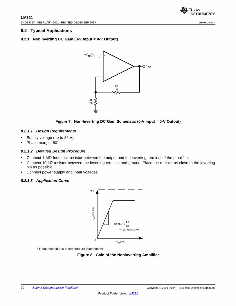
8.2.1 Noninverting DC Gain (0-V Input = 0-V Output)
Figure 7. Non-Inverting DC Gain Schematic (0-V Input = 0-V Output)
8.2.1.1 Design Requirements• Supply voltage (up to 32 V)• Phase margin: 60°
8.2.1.2 Detailed Design Procedure• Connect 1-MΩ feedback resistor between the output and the inverting terminal of the amplifier.• Connect 10-kΩ resistor between the inverting terminal and ground. Place the resistor as close to the inverting
pin as possible.• Connect power supply and input voltages.
8.2.1.3 Application Curve
* R not needed due to temperature independent
Figure 8. Gain of the Noninverting Amplifier
10 Submit Documentation Feedback Copyright © 2001–2014, Texas Instruments Incorporated
Product Folder Links: LM321
LM321www.ti.com SNOS935C –FEBRUARY 2001–REVISED DECEMBER 2014
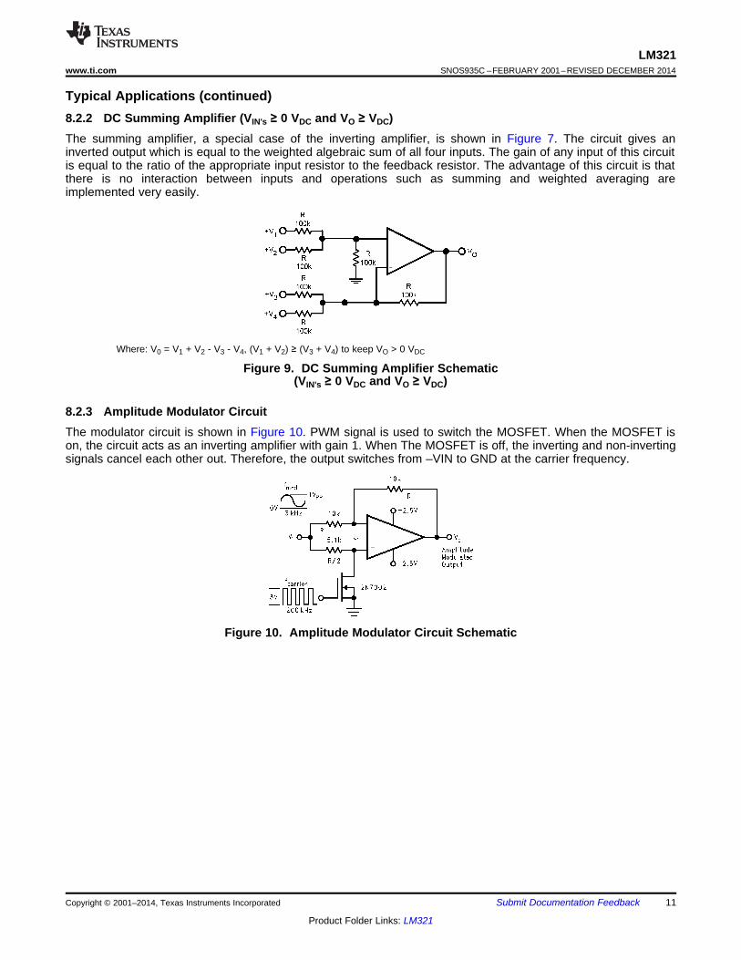
Typical Applications (continued)8.2.2 DC Summing Amplifier (VIN's ≥ 0 VDC and VO ≥ VDC)The summing amplifier, a special case of the inverting amplifier, is shown in Figure 7. The circuit gives aninverted output which is equal to the weighted algebraic sum of all four inputs. The gain of any input of this circuitis equal to the ratio of the appropriate input resistor to the feedback resistor. The advantage of this circuit is thatthere is no interaction between inputs and operations such as summing and weighted averaging areimplemented very easily.
Where: V0 = V1 + V2 - V3 - V4, (V1 + V2) ≥ (V3 + V4) to keep VO > 0 VDC
Figure 9. DC Summing Amplifier Schematic(VIN's ≥ 0 VDC and VO ≥ VDC)
8.2.3 Amplitude Modulator CircuitThe modulator circuit is shown in Figure 10. PWM signal is used to switch the MOSFET. When the MOSFET ison, the circuit acts as an inverting amplifier with gain 1. When The MOSFET is off, the inverting and non-invertingsignals cancel each other out. Therefore, the output switches from –VIN to GND at the carrier frequency.
Figure 10. Amplitude Modulator Circuit Schematic
Copyright © 2001–2014, Texas Instruments Incorporated Submit Documentation Feedback 11
Product Folder Links: LM321

LM321SNOS935C –FEBRUARY 2001–REVISED DECEMBER 2014 www.ti.com
Typical Applications (continued)8.2.4 Power AmplifierPower amplifier application circuit is shown in Figure 11. Voltage gain is set by R1 and R2. The output of theamplifier is connected to the base of BJT which amplifies the current. Current gain is set by β, current gain of aBJT. The resulting output provides high power to the load. Differential voltage supplies are necessary.
V0 = 0 VDC for VIN = 0 VDC, AV = 10
Figure 11. Power Amplifier Schematic
8.2.5 LED DriverLM321 operating as an LED driver is shown in Figure 12. The output of the amplifier sets the current through thediode. The voltage across the LED is assumed constant.
Figure 12. LED Driver Schematic
8.2.6 Fixed Current SourcesOperational amplifier can be used to provide fixed current source to multiple loads. The output voltage of theamplifier is connected to bases of bipolar transistors. The feedback is provided from the drain of a BJT to theinverting terminal of the amplifier. Currents in the second and later BJTs are set by the ratio of R1 and R2.
Figure 13. Fixed Current Sources Schematic
12 Submit Documentation Feedback Copyright © 2001–2014, Texas Instruments Incorporated
Product Folder Links: LM321
LM321www.ti.com SNOS935C –FEBRUARY 2001–REVISED DECEMBER 2014
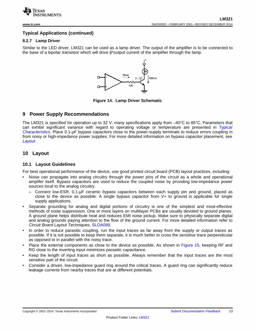
Typical Applications (continued)8.2.7 Lamp DriverSimilar to the LED driver, LM321 can be used as a lamp driver. The output of the amplifier is to be connected tothe base of a bipolar transistor which will drive β*output current of the amplifier through the lamp.
Figure 14. Lamp Driver Schematic
9 Power Supply RecommendationsThe LM321 is specified for operation up to 32 V; many specifications apply from –40°C to 85°C. Parameters thatcan exhibit significant variance with regard to operating voltage or temperature are presented in TypicalCharacteristics. Place 0.1-μF bypass capacitors close to the power-supply terminals to reduce errors coupling infrom noisy or high-impedance power supplies. For more detailed information on bypass capacitor placement, seeLayout.
10 Layout
10.1 Layout GuidelinesFor best operational performance of the device, use good printed circuit board (PCB) layout practices, including:• Noise can propagate into analog circuitry through the power pins of the circuit as a whole and operational
amplifer itself. Bypass capacitors are used to reduce the coupled noise by providing low-impedance powersources local to the analog circuitry.– Connect low-ESR, 0.1-μF ceramic bypass capacitors between each supply pin and ground, placed as
close to the device as possible. A single bypass capacitor from V+ to ground is applicable for singlesupply applications.
• Separate grounding for analog and digital portions of circuitry is one of the simplest and most-effectivemethods of noise suppression. One or more layers on multilayer PCBs are usually devoted to ground planes.A ground plane helps distribute heat and reduces EMI noise pickup. Make sure to physically separate digitaland analog grounds paying attention to the flow of the ground current. For more detailed information refer toCircuit Board Layout Techniques, SLOA089.
• In order to reduce parasitic coupling, run the input traces as far away from the supply or output traces aspossible. If it is not possible to keep them separate, it is much better to cross the sensitive trace perpendicularas opposed to in parallel with the noisy trace.
• Place the external components as close to the device as possible. As shown in Figure 15, keeping RF andRG close to the inverting input minimizes parasitic capacitance.
• Keep the length of input traces as short as possible. Always remember that the input traces are the mostsensitive part of the circuit.
• Consider a driven, low-impedance guard ring around the critical traces. A guard ring can significantly reduceleakage currents from nearby traces that are at different potentials.
Copyright © 2001–2014, Texas Instruments Incorporated Submit Documentation Feedback 13
Product Folder Links: LM321

LM321SNOS935C –FEBRUARY 2001–REVISED DECEMBER 2014 www.ti.com
10.2 Layout Example
Figure 15. PCB Layout Example
14 Submit Documentation Feedback Copyright © 2001–2014, Texas Instruments Incorporated
Product Folder Links: LM321
LM321www.ti.com SNOS935C –FEBRUARY 2001–REVISED DECEMBER 2014
11 Device and Documentation Support
11.1 TrademarksAll trademarks are the property of their respective owners.
11.2 Electrostatic Discharge CautionThese devices have limited built-in ESD protection. The leads should be shorted together or the device placed in conductive foamduring storage or handling to prevent electrostatic damage to the MOS gates.
11.3 GlossarySLYZ022 — TI Glossary.
This glossary lists and explains terms, acronyms, and definitions.
12 Mechanical, Packaging, and Orderable InformationThe following pages include mechanical, packaging, and orderable information. This information is the mostcurrent data available for the designated devices. This data is subject to change without notice and revision ofthis document. For browser-based versions of this data sheet, refer to the left-hand navigation.
Copyright © 2001–2014, Texas Instruments Incorporated Submit Documentation Feedback 15
Product Folder Links: LM321
PACKAGE OPTION ADDENDUM
www.ti.com 2-Aug-2015
Addendum-Page 1
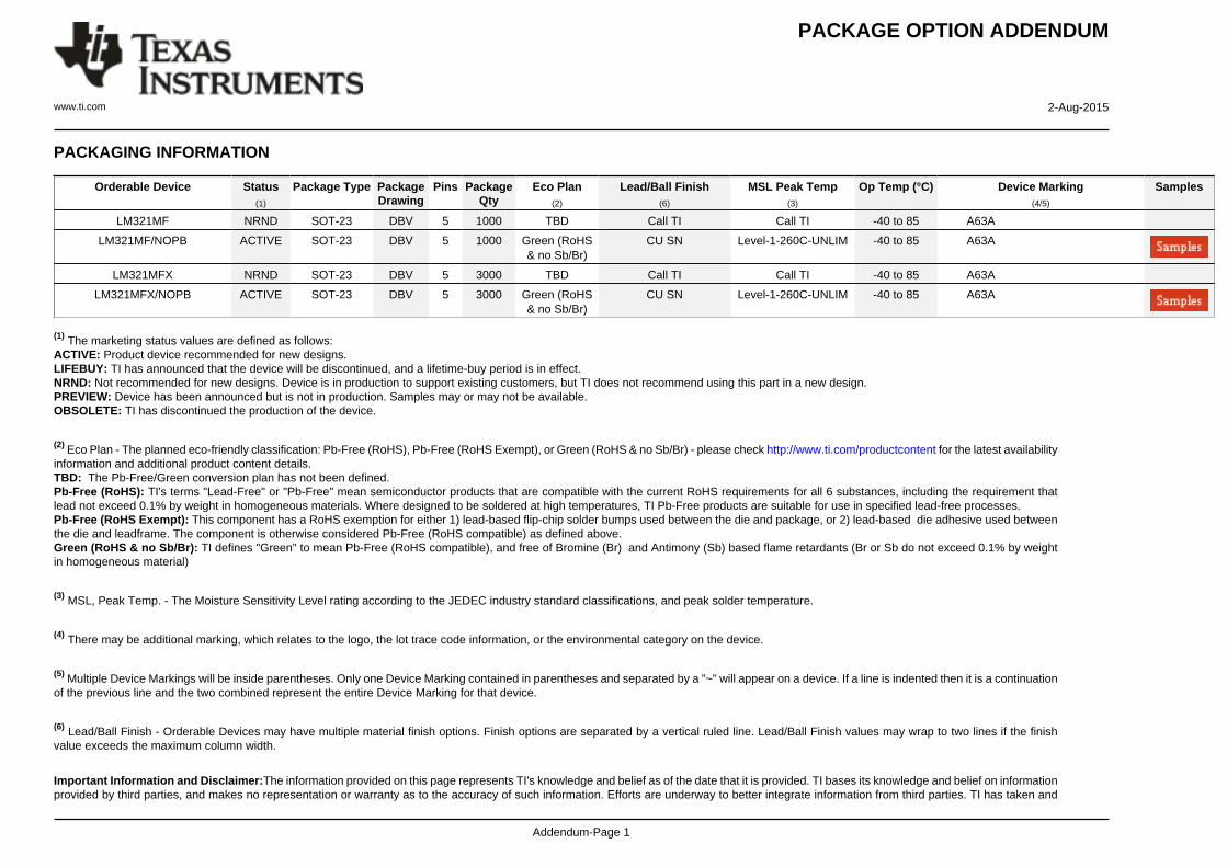
PACKAGING INFORMATION
Orderable Device Status(1)
Package Type PackageDrawing
Pins PackageQty
Eco Plan(2)
Lead/Ball Finish(6)
MSL Peak Temp(3)
Op Temp (°C) Device Marking(4/5)
Samples
LM321MF NRND SOT-23 DBV 5 1000 TBD Call TI Call TI -40 to 85 A63A
LM321MF/NOPB ACTIVE SOT-23 DBV 5 1000 Green (RoHS& no Sb/Br)
CU SN Level-1-260C-UNLIM -40 to 85 A63A
LM321MFX NRND SOT-23 DBV 5 3000 TBD Call TI Call TI -40 to 85 A63A
LM321MFX/NOPB ACTIVE SOT-23 DBV 5 3000 Green (RoHS& no Sb/Br)
CU SN Level-1-260C-UNLIM -40 to 85 A63A
(1) The marketing status values are defined as follows:ACTIVE: Product device recommended for new designs.LIFEBUY: TI has announced that the device will be discontinued, and a lifetime-buy period is in effect.NRND: Not recommended for new designs. Device is in production to support existing customers, but TI does not recommend using this part in a new design.PREVIEW: Device has been announced but is not in production. Samples may or may not be available.OBSOLETE: TI has discontinued the production of the device.
(2) Eco Plan - The planned eco-friendly classification: Pb-Free (RoHS), Pb-Free (RoHS Exempt), or Green (RoHS & no Sb/Br) - please check http://www.ti.com/productcontent for the latest availabilityinformation and additional product content details.TBD: The Pb-Free/Green conversion plan has not been defined.Pb-Free (RoHS): TI's terms "Lead-Free" or "Pb-Free" mean semiconductor products that are compatible with the current RoHS requirements for all 6 substances, including the requirement thatlead not exceed 0.1% by weight in homogeneous materials. Where designed to be soldered at high temperatures, TI Pb-Free products are suitable for use in specified lead-free processes.Pb-Free (RoHS Exempt): This component has a RoHS exemption for either 1) lead-based flip-chip solder bumps used between the die and package, or 2) lead-based die adhesive used betweenthe die and leadframe. The component is otherwise considered Pb-Free (RoHS compatible) as defined above.Green (RoHS & no Sb/Br): TI defines "Green" to mean Pb-Free (RoHS compatible), and free of Bromine (Br) and Antimony (Sb) based flame retardants (Br or Sb do not exceed 0.1% by weightin homogeneous material)
(3) MSL, Peak Temp. - The Moisture Sensitivity Level rating according to the JEDEC industry standard classifications, and peak solder temperature.
(4) There may be additional marking, which relates to the logo, the lot trace code information, or the environmental category on the device.
(5) Multiple Device Markings will be inside parentheses. Only one Device Marking contained in parentheses and separated by a "~" will appear on a device. If a line is indented then it is a continuationof the previous line and the two combined represent the entire Device Marking for that device.
(6) Lead/Ball Finish - Orderable Devices may have multiple material finish options. Finish options are separated by a vertical ruled line. Lead/Ball Finish values may wrap to two lines if the finishvalue exceeds the maximum column width.
Important Information and Disclaimer:The information provided on this page represents TI's knowledge and belief as of the date that it is provided. TI bases its knowledge and belief on informationprovided by third parties, and makes no representation or warranty as to the accuracy of such information. Efforts are underway to better integrate information from third parties. TI has taken and
PACKAGE OPTION ADDENDUM
www.ti.com 2-Aug-2015
Addendum-Page 2
continues to take reasonable steps to provide representative and accurate information but may not have conducted destructive testing or chemical analysis on incoming materials and chemicals.TI and TI suppliers consider certain information to be proprietary, and thus CAS numbers and other limited information may not be available for release.
In no event shall TI's liability arising out of such information exceed the total purchase price of the TI part(s) at issue in this document sold by TI to Customer on an annual basis.
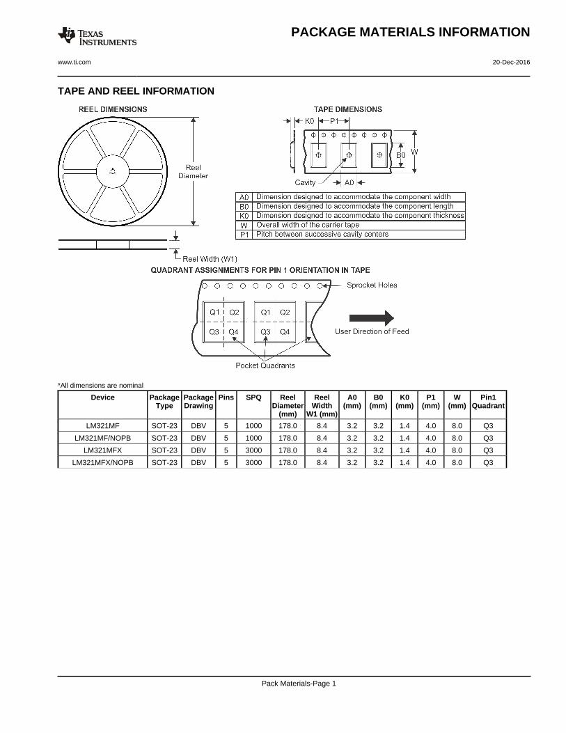
TAPE AND REEL INFORMATION
*All dimensions are nominal
Device PackageType
PackageDrawing
Pins SPQ ReelDiameter
(mm)
ReelWidth
W1 (mm)
A0(mm)
B0(mm)
K0(mm)
P1(mm)
W(mm)
Pin1Quadrant
LM321MF SOT-23 DBV 5 1000 178.0 8.4 3.2 3.2 1.4 4.0 8.0 Q3
LM321MF/NOPB SOT-23 DBV 5 1000 178.0 8.4 3.2 3.2 1.4 4.0 8.0 Q3
LM321MFX SOT-23 DBV 5 3000 178.0 8.4 3.2 3.2 1.4 4.0 8.0 Q3
LM321MFX/NOPB SOT-23 DBV 5 3000 178.0 8.4 3.2 3.2 1.4 4.0 8.0 Q3
PACKAGE MATERIALS INFORMATION
www.ti.com 20-Dec-2016
Pack Materials-Page 1
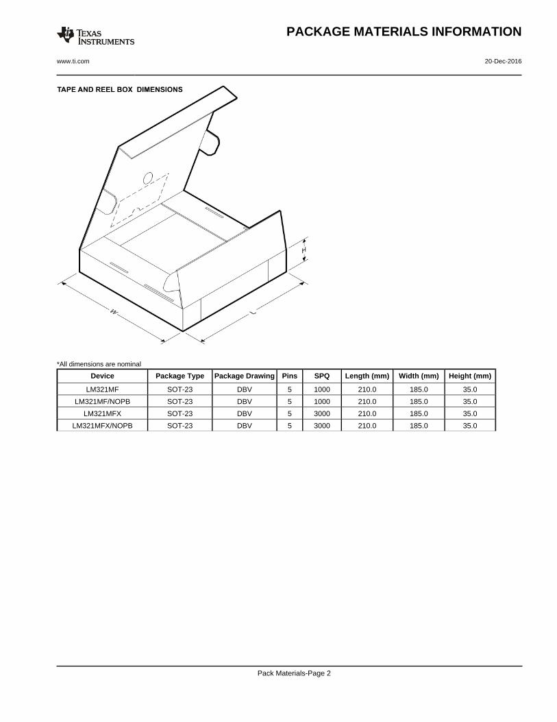
*All dimensions are nominal
Device Package Type Package Drawing Pins SPQ Length (mm) Width (mm) Height (mm)
LM321MF SOT-23 DBV 5 1000 210.0 185.0 35.0
LM321MF/NOPB SOT-23 DBV 5 1000 210.0 185.0 35.0
LM321MFX SOT-23 DBV 5 3000 210.0 185.0 35.0
LM321MFX/NOPB SOT-23 DBV 5 3000 210.0 185.0 35.0
PACKAGE MATERIALS INFORMATION
www.ti.com 20-Dec-2016
Pack Materials-Page 2

www.ti.com
PACKAGE OUTLINE
C
TYP0.220.08
0.25
3.02.6
2X 0.95
1.9
1.45 MAX
TYP0.150.00
5X 0.50.3
TYP0.60.3
TYP80
1.9
A
3.052.75
B1.751.45
(1.1)
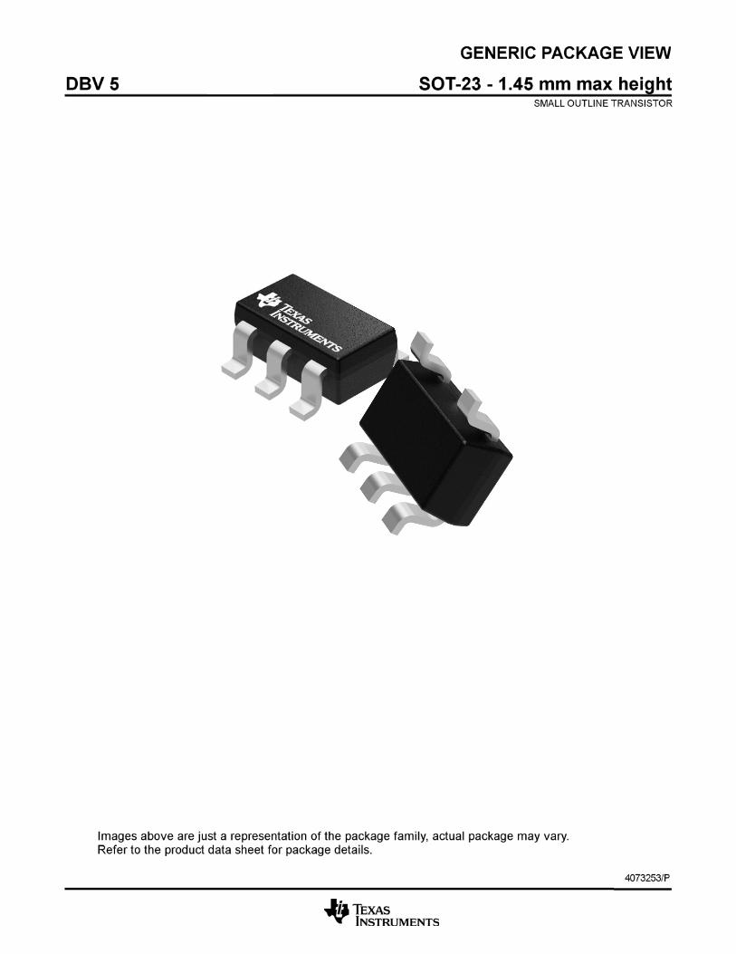
SOT-23 - 1.45 mm max heightDBV0005ASMALL OUTLINE TRANSISTOR
4214839/C 04/2017
NOTES: 1. All linear dimensions are in millimeters. Any dimensions in parenthesis are for reference only. Dimensioning and tolerancing per ASME Y14.5M.2. This drawing is subject to change without notice.3. Refernce JEDEC MO-178.
0.2 C A B
1
34
5
2
INDEX AREAPIN 1
GAGE PLANE
SEATING PLANE
0.1 C
SCALE 4.000

www.ti.com
EXAMPLE BOARD LAYOUT
0.07 MAXARROUND
0.07 MINARROUND
5X (1.1)
5X (0.6)
(2.6)
(1.9)
2X (0.95)
(R0.05) TYP
4214839/C 04/2017
SOT-23 - 1.45 mm max heightDBV0005ASMALL OUTLINE TRANSISTOR
NOTES: (continued) 4. Publication IPC-7351 may have alternate designs. 5. Solder mask tolerances between and around signal pads can vary based on board fabrication site.
SYMM
LAND PATTERN EXAMPLEEXPOSED METAL SHOWN
SCALE:15X
PKG
1
3 4
5
2
SOLDER MASKOPENINGMETAL UNDER
SOLDER MASK
SOLDER MASKDEFINED
EXPOSED METAL
METALSOLDER MASKOPENING
NON SOLDER MASKDEFINED
(PREFERRED)
SOLDER MASK DETAILS
EXPOSED METAL

www.ti.com
EXAMPLE STENCIL DESIGN
(2.6)
(1.9)
2X(0.95)
5X (1.1)
5X (0.6)
(R0.05) TYP
SOT-23 - 1.45 mm max heightDBV0005ASMALL OUTLINE TRANSISTOR
4214839/C 04/2017
NOTES: (continued) 6. Laser cutting apertures with trapezoidal walls and rounded corners may offer better paste release. IPC-7525 may have alternate design recommendations. 7. Board assembly site may have different recommendations for stencil design.
SOLDER PASTE EXAMPLEBASED ON 0.125 mm THICK STENCIL
SCALE:15X
SYMM
PKG
1
3 4
5
2

IMPORTANT NOTICE
Texas Instruments Incorporated (TI) reserves the right to make corrections, enhancements, improvements and other changes to itssemiconductor products and services per JESD46, latest issue, and to discontinue any product or service per JESD48, latest issue. Buyersshould obtain the latest relevant information before placing orders and should verify that such information is current and complete.TI’s published terms of sale for semiconductor products (http://www.ti.com/sc/docs/stdterms.htm) apply to the sale of packaged integratedcircuit products that TI has qualified and released to market. Additional terms may apply to the use or sale of other types of TI products andservices.Reproduction of significant portions of TI information in TI data sheets is permissible only if reproduction is without alteration and isaccompanied by all associated warranties, conditions, limitations, and notices. TI is not responsible or liable for such reproduceddocumentation. Information of third parties may be subject to additional restrictions. Resale of TI products or services with statementsdifferent from or beyond the parameters stated by TI for that product or service voids all express and any implied warranties for theassociated TI product or service and is an unfair and deceptive business practice. TI is not responsible or liable for any such statements.Buyers and others who are developing systems that incorporate TI products (collectively, “Designers”) understand and agree that Designersremain responsible for using their independent analysis, evaluation and judgment in designing their applications and that Designers havefull and exclusive responsibility to assure the safety of Designers' applications and compliance of their applications (and of all TI productsused in or for Designers’ applications) with all applicable regulations, laws and other applicable requirements. Designer represents that, withrespect to their applications, Designer has all the necessary expertise to create and implement safeguards that (1) anticipate dangerousconsequences of failures, (2) monitor failures and their consequences, and (3) lessen the likelihood of failures that might cause harm andtake appropriate actions. Designer agrees that prior to using or distributing any applications that include TI products, Designer willthoroughly test such applications and the functionality of such TI products as used in such applications.TI’s provision of technical, application or other design advice, quality characterization, reliability data or other services or information,including, but not limited to, reference designs and materials relating to evaluation modules, (collectively, “TI Resources”) are intended toassist designers who are developing applications that incorporate TI products; by downloading, accessing or using TI Resources in anyway, Designer (individually or, if Designer is acting on behalf of a company, Designer’s company) agrees to use any particular TI Resourcesolely for this purpose and subject to the terms of this Notice.TI’s provision of TI Resources does not expand or otherwise alter TI’s applicable published warranties or warranty disclaimers for TIproducts, and no additional obligations or liabilities arise from TI providing such TI Resources. TI reserves the right to make corrections,enhancements, improvements and other changes to its TI Resources. TI has not conducted any testing other than that specificallydescribed in the published documentation for a particular TI Resource.Designer is authorized to use, copy and modify any individual TI Resource only in connection with the development of applications thatinclude the TI product(s) identified in such TI Resource. NO OTHER LICENSE, EXPRESS OR IMPLIED, BY ESTOPPEL OR OTHERWISETO ANY OTHER TI INTELLECTUAL PROPERTY RIGHT, AND NO LICENSE TO ANY TECHNOLOGY OR INTELLECTUAL PROPERTYRIGHT OF TI OR ANY THIRD PARTY IS GRANTED HEREIN, including but not limited to any patent right, copyright, mask work right, orother intellectual property right relating to any combination, machine, or process in which TI products or services are used. Informationregarding or referencing third-party products or services does not constitute a license to use such products or services, or a warranty orendorsement thereof. Use of TI Resources may require a license from a third party under the patents or other intellectual property of thethird party, or a license from TI under the patents or other intellectual property of TI.TI RESOURCES ARE PROVIDED “AS IS” AND WITH ALL FAULTS. TI DISCLAIMS ALL OTHER WARRANTIES ORREPRESENTATIONS, EXPRESS OR IMPLIED, REGARDING RESOURCES OR USE THEREOF, INCLUDING BUT NOT LIMITED TOACCURACY OR COMPLETENESS, TITLE, ANY EPIDEMIC FAILURE WARRANTY AND ANY IMPLIED WARRANTIES OFMERCHANTABILITY, FITNESS FOR A PARTICULAR PURPOSE, AND NON-INFRINGEMENT OF ANY THIRD PARTY INTELLECTUALPROPERTY RIGHTS. TI SHALL NOT BE LIABLE FOR AND SHALL NOT DEFEND OR INDEMNIFY DESIGNER AGAINST ANY CLAIM,INCLUDING BUT NOT LIMITED TO ANY INFRINGEMENT CLAIM THAT RELATES TO OR IS BASED ON ANY COMBINATION OFPRODUCTS EVEN IF DESCRIBED IN TI RESOURCES OR OTHERWISE. IN NO EVENT SHALL TI BE LIABLE FOR ANY ACTUAL,DIRECT, SPECIAL, COLLATERAL, INDIRECT, PUNITIVE, INCIDENTAL, CONSEQUENTIAL OR EXEMPLARY DAMAGES INCONNECTION WITH OR ARISING OUT OF TI RESOURCES OR USE THEREOF, AND REGARDLESS OF WHETHER TI HAS BEENADVISED OF THE POSSIBILITY OF SUCH DAMAGES.Unless TI has explicitly designated an individual product as meeting the requirements of a particular industry standard (e.g., ISO/TS 16949and ISO 26262), TI is not responsible for any failure to meet such industry standard requirements.Where TI specifically promotes products as facilitating functional safety or as compliant with industry functional safety standards, suchproducts are intended to help enable customers to design and create their own applications that meet applicable functional safety standardsand requirements. Using products in an application does not by itself establish any safety features in the application. Designers mustensure compliance with safety-related requirements and standards applicable to their applications. Designer may not use any TI products inlife-critical medical equipment unless authorized officers of the parties have executed a special contract specifically governing such use.Life-critical medical equipment is medical equipment where failure of such equipment would cause serious bodily injury or death (e.g., lifesupport, pacemakers, defibrillators, heart pumps, neurostimulators, and implantables). Such equipment includes, without limitation, allmedical devices identified by the U.S. Food and Drug Administration as Class III devices and equivalent classifications outside the U.S.TI may expressly designate certain products as completing a particular qualification (e.g., Q100, Military Grade, or Enhanced Product).Designers agree that it has the necessary expertise to select the product with the appropriate qualification designation for their applicationsand that proper product selection is at Designers’ own risk. Designers are solely responsible for compliance with all legal and regulatoryrequirements in connection with such selection.Designer will fully indemnify TI and its representatives against any damages, costs, losses, and/or liabilities arising out of Designer’s non-compliance with the terms and provisions of this Notice.
Mailing Address: Texas Instruments, Post Office Box 655303, Dallas, Texas 75265Copyright © 2018, Texas Instruments Incorporated