Embed Size (px)
Citation preview

VIN
SW
BSTLM2695
VCC
SS
RON/SD
8V - 30VInput
C1
RON
R2
R1
C2
VOUTL1
C3
C4
D1
C6
RTN
ISEN
SGND
FB
SHUTDOWN
R3
LM2695
www.ti.com SNVS413A –JANUARY 2006–REVISED APRIL 2013
LM2695 High Voltage (30V, 1.25A) Step Down Switching RegulatorCheck for Samples: LM2695
1FEATURES DESCRIPTIONThe LM2695 Step Down Switching Regulator features
2• Integrated 33V, N-Channel Buck Switchall of the functions needed to implement a low cost,
• Integrated Start-Up Regulator efficient, buck bias regulator capable of supplying• Input Voltage Range: 8V to 30V 1.25A to the load. This buck regulator contains a 33V
N-Channel Buck Switch, and is available in the• No Loop Compensation Requiredthermally enhanced WSON-10 and HTSSOP-14• Ultra-Fast Transient Response packages. The hysteretic regulation scheme requires
• Operating Frequency Remains Constant with no loop compensation, results in fast load transientLoad Current and Input Voltage response, and simplifies circuit implementation. The
operating frequency remains constant with line and• Maximum Duty Cycle Limited During Start-Upload variations due to the inverse relationship• Adjustable Output Voltage between the input voltage and the on-time. The
• Valley Current Limit At 1.25A current limit detection is set at 1.25A. Additionalfeatures include: VCC under-voltage lockout, thermal• Precision Internal Referenceshutdown, gate drive under-voltage lockout, and• Low Bias Currentmaximum duty cycle limiter.
• Highly Efficient Operation• Thermal Shutdown PACKAGE
• 10-Pin WSON (4 mm x 4 mm)TYPICAL APPLICATIONS• 14-Pin HTSSOP
• High Efficiency Point-Of-Load (POL) Regulator• Exposed Thermal Pad For Improved Heat
• Non-Isolated Telecommunication Buck DissipationRegulator
• Secondary High Voltage Post Regulator
Basic Step Down Regulator
1
Please be aware that an important notice concerning availability, standard warranty, and use in critical applications ofTexas Instruments semiconductor products and disclaimers thereto appears at the end of this data sheet.
2All trademarks are the property of their respective owners.
PRODUCTION DATA information is current as of publication date. Copyright © 2006–2013, Texas Instruments IncorporatedProducts conform to specifications per the terms of the TexasInstruments standard warranty. Production processing does notnecessarily include testing of all parameters.
SW
BST
NC
NC NC
NC
RTN FB
SS
11
10
9
5
4
3
2
1
6
7 8
12
13
14
VCC
VIN
RON/SD
SGND
ISEN
SW
BST
RTN
VCC
FB
SS
VIN10
9
8
7
65
4
3
2
1
RON/SD
SGND
ISEN
LM2695
SNVS413A –JANUARY 2006–REVISED APRIL 2013 www.ti.com
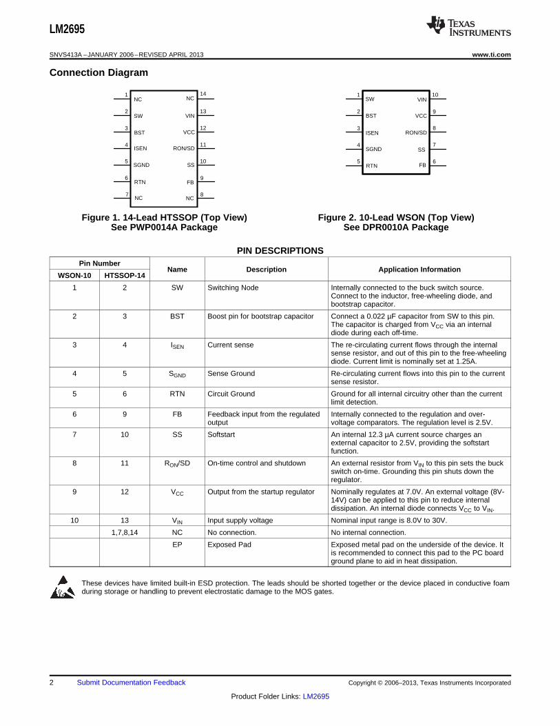
Connection Diagram
Figure 1. 14-Lead HTSSOP (Top View) Figure 2. 10-Lead WSON (Top View)See PWP0014A Package See DPR0010A Package
PIN DESCRIPTIONSPin Number
Name Description Application InformationWSON-10 HTSSOP-14
1 2 SW Switching Node Internally connected to the buck switch source.Connect to the inductor, free-wheeling diode, andbootstrap capacitor.
2 3 BST Boost pin for bootstrap capacitor Connect a 0.022 µF capacitor from SW to this pin.The capacitor is charged from VCC via an internaldiode during each off-time.
3 4 ISEN Current sense The re-circulating current flows through the internalsense resistor, and out of this pin to the free-wheelingdiode. Current limit is nominally set at 1.25A.
4 5 SGND Sense Ground Re-circulating current flows into this pin to the currentsense resistor.
5 6 RTN Circuit Ground Ground for all internal circuitry other than the currentlimit detection.
6 9 FB Feedback input from the regulated Internally connected to the regulation and over-output voltage comparators. The regulation level is 2.5V.
7 10 SS Softstart An internal 12.3 µA current source charges anexternal capacitor to 2.5V, providing the softstartfunction.
8 11 RON/SD On-time control and shutdown An external resistor from VIN to this pin sets the buckswitch on-time. Grounding this pin shuts down theregulator.
9 12 VCC Output from the startup regulator Nominally regulates at 7.0V. An external voltage (8V-14V) can be applied to this pin to reduce internaldissipation. An internal diode connects VCC to VIN.
10 13 VIN Input supply voltage Nominal input range is 8.0V to 30V.
1,7,8,14 NC No connection. No internal connection.
EP Exposed Pad Exposed metal pad on the underside of the device. Itis recommended to connect this pad to the PC boardground plane to aid in heat dissipation.
These devices have limited built-in ESD protection. The leads should be shorted together or the device placed in conductive foamduring storage or handling to prevent electrostatic damage to the MOS gates.
2 Submit Documentation Feedback Copyright © 2006–2013, Texas Instruments Incorporated
Product Folder Links: LM2695

LM2695
www.ti.com SNVS413A –JANUARY 2006–REVISED APRIL 2013
Absolute Maximum Ratings (1) (2) (3)
VIN to RTN 33V
BST to RTN 47V
SW to RTN (Steady State) -1.5V
ESD Rating (4) Human Body Model 2kV
BST to VCC 33V
VIN to SW 33V
BST to SW 14V
VCC to RTN 14V
SGND to RTN -0.3V to +0.3V
Current out of ISEN See Text
SS to RTN -0.3V to 4V
All Other Inputs to RTN -0.3 to 7V
Storage Temperature Range -65°C to +150°C
Junction Temperature 150°C
(1) Absolute Maximum Ratings are limits beyond which damage to the device may occur. Operating Ratings are conditions under whichoperation of the device is intended to be functional. For ensured specifications and test conditions, see the Electrical Characteristics.
(2) For detailed information on soldering plastic WSON-10 packages, refer to the Packaging Data Book available from TI.(3) If Military/Aerospace specified devices are required, please contact the TI Sales Office/Distributors for availability and specifications.(4) The human body model is a 100pF capacitor discharged through a 1.5kΩ resistor into each pin.
Operating Ratings (1)
VIN 8.0V to 30V
Junction Temperature −40°C to + 125°C
(1) Absolute Maximum Ratings are limits beyond which damage to the device may occur. Operating Ratings are conditions under whichoperation of the device is intended to be functional. For ensured specifications and test conditions, see the Electrical Characteristics.
Copyright © 2006–2013, Texas Instruments Incorporated Submit Documentation Feedback 3
Product Folder Links: LM2695
LM2695
SNVS413A –JANUARY 2006–REVISED APRIL 2013 www.ti.com
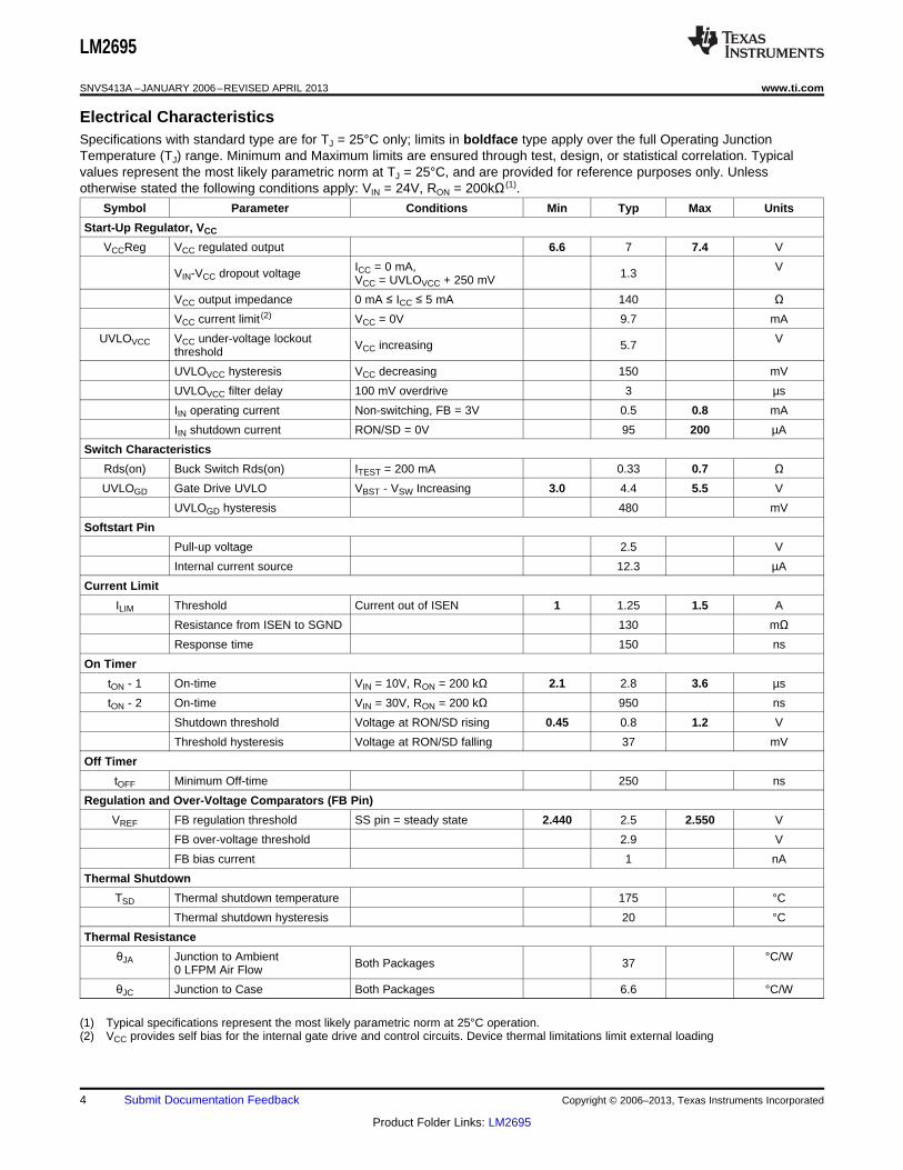
Electrical CharacteristicsSpecifications with standard type are for TJ = 25°C only; limits in boldface type apply over the full Operating JunctionTemperature (TJ) range. Minimum and Maximum limits are ensured through test, design, or statistical correlation. Typicalvalues represent the most likely parametric norm at TJ = 25°C, and are provided for reference purposes only. Unlessotherwise stated the following conditions apply: VIN = 24V, RON = 200kΩ (1).
Symbol Parameter Conditions Min Typ Max Units
Start-Up Regulator, VCC
VCCReg VCC regulated output 6.6 7 7.4 V
ICC = 0 mA, VVIN-VCC dropout voltage 1.3VCC = UVLOVCC + 250 mV
VCC output impedance 0 mA ≤ ICC ≤ 5 mA 140 ΩVCC current limit (2) VCC = 0V 9.7 mA
UVLOVCC VCC under-voltage lockout VVCC increasing 5.7threshold
UVLOVCC hysteresis VCC decreasing 150 mV
UVLOVCC filter delay 100 mV overdrive 3 µs
IIN operating current Non-switching, FB = 3V 0.5 0.8 mA
IIN shutdown current RON/SD = 0V 95 200 µA
Switch Characteristics
Rds(on) Buck Switch Rds(on) ITEST = 200 mA 0.33 0.7 ΩUVLOGD Gate Drive UVLO VBST - VSW Increasing 3.0 4.4 5.5 V
UVLOGD hysteresis 480 mV
Softstart Pin
Pull-up voltage 2.5 V
Internal current source 12.3 µA
Current Limit
ILIM Threshold Current out of ISEN 1 1.25 1.5 A
Resistance from ISEN to SGND 130 mΩResponse time 150 ns
On Timer
tON - 1 On-time VIN = 10V, RON = 200 kΩ 2.1 2.8 3.6 µs
tON - 2 On-time VIN = 30V, RON = 200 kΩ 950 ns
Shutdown threshold Voltage at RON/SD rising 0.45 0.8 1.2 V
Threshold hysteresis Voltage at RON/SD falling 37 mV
Off Timer
tOFF Minimum Off-time 250 ns
Regulation and Over-Voltage Comparators (FB Pin)
VREF FB regulation threshold SS pin = steady state 2.440 2.5 2.550 V
FB over-voltage threshold 2.9 V
FB bias current 1 nA
Thermal Shutdown
TSD Thermal shutdown temperature 175 °C
Thermal shutdown hysteresis 20 °C
Thermal Resistance
θJA Junction to Ambient °C/WBoth Packages 370 LFPM Air Flow
θJC Junction to Case Both Packages 6.6 °C/W
(1) Typical specifications represent the most likely parametric norm at 25°C operation.(2) VCC provides self bias for the internal gate drive and control circuits. Device thermal limitations limit external loading
4 Submit Documentation Feedback Copyright © 2006–2013, Texas Instruments Incorporated
Product Folder Links: LM2695

LM2695
ON TIMER 250 nsOFF TIMER
LEVELSHIFT
THERMALSHUTDOWN
7V SERIESREGULATOR
VCCUVLO
8V-30VInput
VIN
C1
RON
C5
RON/SD
SS
FB
RTN
LOGIC
REGULATIONCOMPARATOR
OVER-VOLTAGE
COMPARATOR
+-
+-
+-
D1
SGND
ISEN
SW
BST
VCC
VIN
COMPLETESTART
RON STARTCOMPLETE
C3
C4
R1
R2
R3
C2
CURRENT LIMITCOMPARATOR
RSENSE50 m:
VOUT1
VOUT22.9V
2.5V
12.3 PA
GATE DRIVEUVLO
L1
+-
+-
0.8V
DRIVER
DRIVER
62.5 mV
C6
6.5 7.0 7.5 8.0 8.5 9.05.0
5.5
6.0
6.5
7.0
7.5V
CC
(V
)
VIN (V)
FS = 750 kHz
FS = 45 kHz
FS = 150 kHz
0 10 20 30
VIN (V)
0
1.0
2.0
3.0
4.0
5.0
6.0
7.0
ON
-TIM
E (P
s)
RON = 400k
RON = 200k
RON = 100k
RON = 44.2k
LM2695
www.ti.com SNVS413A –JANUARY 2006–REVISED APRIL 2013
Typical Performance Characteristics
Figure 3. VCC vs VIN Figure 4. ON-Time vs VIN and RON
Typical Application Circuit and Block Diagram
Copyright © 2006–2013, Texas Instruments Incorporated Submit Documentation Feedback 5
Product Folder Links: LM2695

FS =VOUT
2 x L1 x 1.18 x 1020
RL x (RON)2
DC =tON
tON + tOFF
=VOUT
VIN
FS =VOUT
1.3 x 10⁻¹⁰ x RON
LM2695
SNVS413A –JANUARY 2006–REVISED APRIL 2013 www.ti.com
Functional Description
The LM2695 Step Down Switching Regulator features all the functions needed to implement a low cost, efficientbuck bias power converter capable of supplying 1.25A to the load. This high voltage regulator contains a 33V N-Channel buck switch, is easy to implement, and is available in the thermally enhanced WSON-10 and HTSSOP-14 packages. The regulator’s operation is based on a hysteretic control scheme, and uses an on-time controlwhich varies inversely with VIN. This feature allows the operating frequency to remain relatively constant withload and input voltage variations. The hysteretic control requires no loop compensation resulting in very fast loadtransient response. The valley current limit detection circuit, internally set at 1.25A, holds the buck switch off untilthe high current level subsides. The functional block diagram is shown in Typical Application Circuit and BlockDiagram.
The LM2695 can be applied in numerous applications to efficiently regulate down higher voltages. Additionalfeatures include: Thermal shutdown, VCC under-voltage lockout, gate drive under-voltage lockout, and maximumduty cycle limiter.
Hysteretic Control Circuit Overview
The LM2695 buck DC-DC regulator employs a control scheme based on a comparator and a one-shot on-timer,with the output voltage feedback (FB) compared to an internal reference (2.5V). If the FB voltage is below thereference the buck switch is turned on for a time period determined by the input voltage and a programmingresistor (RON). Following the on-time the switch remains off for a minimum of 250 ns, and until the FB voltagefalls below the reference. The buck switch then turns on for another on-time period. Typically, during start-up, orwhen the load current increases suddenly, the off-times are at the minimum of 250 ns. Once regulation isestablished, the off-times are longer.
When in regulation, the LM2695 operates in continuous conduction mode at heavy load currents anddiscontinuous conduction mode at light load currents. In continuous conduction mode current always flowsthrough the inductor, never reaching zero during the off-time. In this mode the operating frequency remainsrelatively constant with load and line variations. The minimum load current for continuous conduction mode isone-half the inductor’s ripple current amplitude. The operating frequency is approximately:
(1)
The buck switch duty cycle is equal to:
(2)
In discontinuous conduction mode current through the inductor ramps up from zero to a peak during the on-time,then ramps back to zero before the end of the off-time. The next on-time period starts when the voltage at FBfalls below the reference - until then the inductor current remains zero, and the load current is supplied by theoutput capacitor (C2). In this mode the operating frequency is lower than in continuous conduction mode, andvaries with load current. Conversion efficiency is maintained at light loads since the switching losses reduce withthe reduction in load and frequency. The approximate discontinuous operating frequency can be calculated asfollows:
where• RL = the load resistance (3)
The output voltage is set by two external resistors (R1, R2). The regulated output voltage is calculated asfollows:
VOUT = 2.5 x (R1 + R2) / R2 (4)
6 Submit Documentation Feedback Copyright © 2006–2013, Texas Instruments Incorporated
Product Folder Links: LM2695
FB
SW
L1
C2
R1
R2
VOUT2
R3LM2695
LM2695
www.ti.com SNVS413A –JANUARY 2006–REVISED APRIL 2013
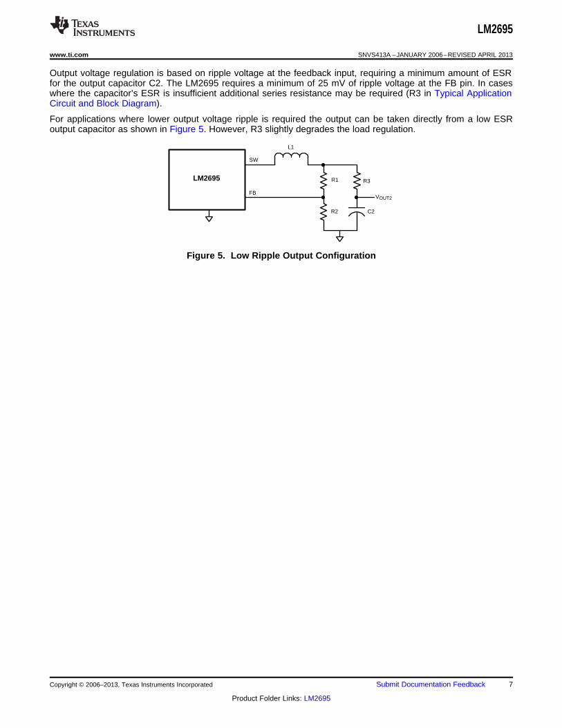
Output voltage regulation is based on ripple voltage at the feedback input, requiring a minimum amount of ESRfor the output capacitor C2. The LM2695 requires a minimum of 25 mV of ripple voltage at the FB pin. In caseswhere the capacitor’s ESR is insufficient additional series resistance may be required (R3 in Typical ApplicationCircuit and Block Diagram).
For applications where lower output voltage ripple is required the output can be taken directly from a low ESRoutput capacitor as shown in Figure 5. However, R3 slightly degrades the load regulation.
Figure 5. Low Ripple Output Configuration
Copyright © 2006–2013, Texas Instruments Incorporated Submit Documentation Feedback 7
Product Folder Links: LM2695
tON =VIN
1.3 x 10⁻¹⁰ x RON
FB
SW
L1
C2
R1
R2
R3
LM2695
BST
VCC
D2
C3
C4
D1ISEN
SGND
VOUT1
LM2695
SNVS413A –JANUARY 2006–REVISED APRIL 2013 www.ti.com
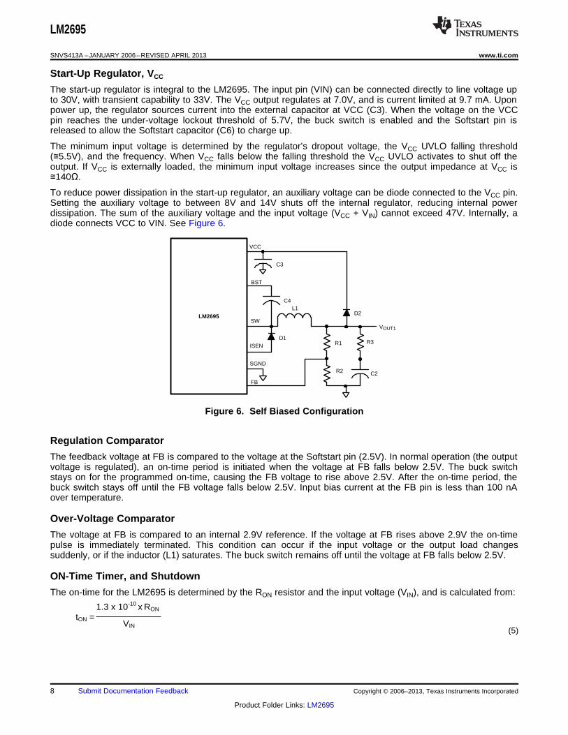
Start-Up Regulator, VCC
The start-up regulator is integral to the LM2695. The input pin (VIN) can be connected directly to line voltage upto 30V, with transient capability to 33V. The VCC output regulates at 7.0V, and is current limited at 9.7 mA. Uponpower up, the regulator sources current into the external capacitor at VCC (C3). When the voltage on the VCCpin reaches the under-voltage lockout threshold of 5.7V, the buck switch is enabled and the Softstart pin isreleased to allow the Softstart capacitor (C6) to charge up.
The minimum input voltage is determined by the regulator’s dropout voltage, the VCC UVLO falling threshold(≊5.5V), and the frequency. When VCC falls below the falling threshold the VCC UVLO activates to shut off theoutput. If VCC is externally loaded, the minimum input voltage increases since the output impedance at VCC is≊140Ω.
To reduce power dissipation in the start-up regulator, an auxiliary voltage can be diode connected to the VCC pin.Setting the auxiliary voltage to between 8V and 14V shuts off the internal regulator, reducing internal powerdissipation. The sum of the auxiliary voltage and the input voltage (VCC + VIN) cannot exceed 47V. Internally, adiode connects VCC to VIN. See Figure 6.
Figure 6. Self Biased Configuration
Regulation Comparator
The feedback voltage at FB is compared to the voltage at the Softstart pin (2.5V). In normal operation (the outputvoltage is regulated), an on-time period is initiated when the voltage at FB falls below 2.5V. The buck switchstays on for the programmed on-time, causing the FB voltage to rise above 2.5V. After the on-time period, thebuck switch stays off until the FB voltage falls below 2.5V. Input bias current at the FB pin is less than 100 nAover temperature.
Over-Voltage Comparator
The voltage at FB is compared to an internal 2.9V reference. If the voltage at FB rises above 2.9V the on-timepulse is immediately terminated. This condition can occur if the input voltage or the output load changessuddenly, or if the inductor (L1) saturates. The buck switch remains off until the voltage at FB falls below 2.5V.
ON-Time Timer, and Shutdown
The on-time for the LM2695 is determined by the RON resistor and the input voltage (VIN), and is calculated from:
(5)
8 Submit Documentation Feedback Copyright © 2006–2013, Texas Instruments Incorporated
Product Folder Links: LM2695

STOP
RUN
RON/SD
InputVoltage
LM2695
VIN
RON
tON(min) =VOUT x 288 ns
(VIN(min) - VOUT)
RON =VOUT
FS x 1.3 x 10⁻¹⁰
LM2695
www.ti.com SNVS413A –JANUARY 2006–REVISED APRIL 2013
See Figure 4. The inverse relationship with VIN results in a nearly constant frequency as VIN is varied. To set aspecific continuous conduction mode switching frequency (FS), the RON resistor is determined from the following:
(6)
In high frequency applicatons the minimum value for tON is limited by the maximum duty cycle required forregulation and the minimum off-time of (250 ns, ±15%). The minimum off-time limits the maximum duty cycleachievable with a low voltage at VIN. The minimum allowed on-time to regulate the desired VOUT at the minimumVIN is determined from the following:
(7)
The LM2695 can be remotely shut down by taking the RON/SD pin below 0.8V. See Figure 7. In this mode theSS pin is internally grounded, the on-timer is disabled, and bias currents are reduced. Releasing the RON/SD pinallows normal operation to resume. The voltage at the RON/SD pin is between 1.5V and 3.0V, depending on VINand the RON resistor.
Figure 7. Shutdown Implementation
Current Limit
Current limit detection occurs during the off-time by monitoring the recirculating current through the free-wheelingdiode (D1). Referring to Typical Application Circuit and Block Diagram, when the buck switch is turned off theinductor current flows through the load, into SGND, through the sense resistor, out of ISEN and through D1. Ifthat current exceeds 1.25A the current limit comparator output switches to delay the start of the next on-timeperiod if the voltage at FB is below 2.5V. The next on-time starts when the current out of ISEN is below 1.25Aand the voltage at FB is below 2.5V. If the overload condition persists causing the inductor current to exceed1.25A during each on-time, that is detected at the beginning of each off-time. The operating frequency is lowerdue to longer-than-normal off-times.
Figure 8 illustrates the inductor current waveform. During normal operation the load current is Io, the average ofthe ripple waveform. When the load resistance decreases the current ratchets up until the lower peak reaches1.25A. During the Current Limited portion of Figure 8, the current ramps down to 1.25A during each off-time,initiating the next on-time (assuming the voltage at FB is <2.5V). During each on-time the current ramps up anamount equal to:
ΔI = (VIN - VOUT) x tON / L1 (8)
During this time the LM2695 is in a constant current mode, with an average load current (IOCL) equal to 1.25A +ΔI/2.
Copyright © 2006–2013, Texas Instruments Incorporated Submit Documentation Feedback 9
Product Folder Links: LM2695

1.25A
Load CurrentIncreases
IPK
IOCL
IO
'I
Normal Operation Current Limited
Indu
ctor
Cur
rent
LM2695
SNVS413A –JANUARY 2006–REVISED APRIL 2013 www.ti.com
Figure 8. Inductor Current - Current Limit Operation
The current limit threshold can be increased by connecting an external resistor between SGND and ISEN. Theexternal resistor will typically be less than 1Ω. The peak current out of SW and ISEN must not exceed 2A. Theaverage current out of SW must be less than 1.5A.
N - Channel Buck Switch and Driver
The LM2695 integrates an N-Channel buck switch and associated floating high voltage gate driver. The peakcurrent allowed through the buck switch is 2A, and the maximum allowed average current is 1.5A. The gatedriver circuit works in conjunction with an external bootstrap capacitor and an internal high voltage diode. A 0.022µF capacitor (C4) connected between BST and SW provides the voltage to the driver during the on-time. Duringeach off-time, the SW pin is at approximately -1V, and C4 charges from VCC through the internal diode. Theminimum off-time of 250 ns ensures a minimum time each cycle to recharge the bootstrap capacitor.
Softstart
The softstart feature allows the converter to gradually reach a steady state operating point, thereby reducingstart-up stresses and current surges. Upon turn-on, after VCC reaches the under-voltage threshold, an internal12.3 µA current source charges up the external capacitor at the SS pin to 2.5V. The ramping voltage at SS (andthe non-inverting input of the regulation comparator) ramps up the output voltage in a controlled manner.
An internal switch grounds the SS pin if VCC is below the under-voltage lockout threshold, if a thermal shutdownoccurs, or if the RON/SD pin is grounded.
Thermal Shutdown
The LM2695 should be operated so the junction temperature does not exceed 125°C. If the junction temperatureincreases, an internal Thermal Shutdown circuit, which activates (typically) at 175°C, takes the controller to a lowpower reset state by disabling the buck switch and the on-timer, and grounding the Softstart pin. This featurehelps prevent catastrophic failures from accidental device overheating. When the junction temperature reducesbelow 155°C (typical hysteresis = 20°C), the Softstart pin is released and normal operation resumes.
10 Submit Documentation Feedback Copyright © 2006–2013, Texas Instruments Incorporated
Product Folder Links: LM2695

ESR(min) =25 mV x (R1 + R2)
R2 x IOR(min)
L1 =VOUT x (VIN - VOUT)
IOR x FS x VIN
RON 200 ns x VIN(MAX)
t1.3 x 10-10
LM2695
www.ti.com SNVS413A –JANUARY 2006–REVISED APRIL 2013
APPLICATIONS INFORMATION
EXTERNAL COMPONENTS
The following guidelines can be used to select the external components.
R1 and R2: The ratio of these resistors is calculated from:R1/R2 = (VOUT/2.5V) - 1 (9)
R1 and R2 should be chosen from standard value resistors in the range of 1.0 kΩ - 10 kΩ which satisfy theabove ratio.
RON: The minimum value for RON is calculated from:
(10)
Equation 1 can be used to select RON if a specific frequency is desired as long as the above limitation is met.
L1: The main parameter affected by the inductor is the output current ripple amplitude (IOR). The limits for IORmust be determined at both the minimum and maximum nominal load currents.
a) If the maximum load current is less than the current limit threshold (1.25A), the minimum load current is usedto determine the maximum allowable ripple. To maintain continuous conduction mode the lower peak should notreach 0 mA. For this case, the maximum ripple current is:
IOR(MAX1) = 2 x IO(min) (11)
The ripple calculated in Equation 11 is then used in the following equation:
where• VIN is the maximum input voltage• Fs is determined from Equation 1 (12)
This provides a minimum value for L1. The next larger standard value should be used, and L1 should be ratedfor the IPK current level.
b) If the maximum load current is greater than the current limit threshold (1.25A), the LM2695 ensures the lowerpeak reaches 1.25A each cycle, requiring that IOR be at least twice the difference. The upper peak, however,must not exceed 2A. For this case, the ripple limits are:
IOR(MAX2) = 2 x (2A - IO(max)) (13)
andIOR(MIN1) = 2 x (IO(max) - 1.25A) (14)
The lesser of Equation 13 and Equation 14 is then used in Equation 12. If IOR(MAX2) is used, the maximum VIN isused in Equation 12. The next larger value should then be used for L1. If IOR(MIN1) is used, the minimum VIN isused in Equation 12. The next smaller value should then be used for L1. L1 must be rated for the peak value ofthe current waveform (IPK in Figure 8).
C3: The capacitor at the VCC output provides not only noise filtering and stability, but also prevents falsetriggering of the VCC UVLO at the buck switch on/off transitions. For this reason, C3 should be no smaller than0.1 µF, and should be a good quality, low ESR, ceramic capacitor.
C2, and R3: Since the LM2695 requires a minimum of 25 mVp-p of ripple at the FB pin for proper operation, therequired ripple at VOUT1 is increased by R1 and R2. This necessary ripple is created by the inductor ripple currentacting on C2’s ESR + R3. The minimum ripple current is calculated using Equation 12, rearranged to solve forIOR at minimum VIN. The minimum ESR for C2 is then equal to:
(15)
Copyright © 2006–2013, Texas Instruments Incorporated Submit Documentation Feedback 11
Product Folder Links: LM2695
tSS =C6 x 2.5V12.3 PA
C1 =IO x tON
'V
LM2695
SNVS413A –JANUARY 2006–REVISED APRIL 2013 www.ti.com
If the capacitor used for C2 does not have sufficient ESR, R3 is added in series as shown in Typical ApplicationCircuit and Block Diagram. Generally R3 is less than 1Ω. C2 should generally be no smaller than 3.3 µF,although that is dependent on the frequency and the allowable ripple amplitude at VOUT1. Experimentation isusually necessary to determine the minimum value for C2, as the nature of the load may require a larger value. Aload which creates significant transients requires a larger value for C2 than a non-varying load.
D1: The important parameters are reverse recovery time and forward voltage. The reverse recovery timedetermines how long the reverse current surge lasts each time the buck switch is turned on. The forward voltagedrop is significant in the event the output is short-circuited as it is mainly this diode’s voltage (plus the voltageacross the current limit sense resistor) which forces the inductor current to decrease during the off-time. For thisreason, a higher voltage is better, although that affects efficiency. A reverse recovery time of ≊30 ns, and aforward voltage drop of ≊0.75V are preferred. The reverse leakage specification is important as that cansignificantly affect efficiency. D1’s reverse voltage rating must be at least as great as the maximum VIN, and itscurrent rating must equal or exceed IPK Figure 8.
C1 and C5: C1’s purpose is to supply most of the switch current during the on-time, and limit the voltage rippleat VIN, on the assumption that the voltage source feeding VIN has an output impedance greater than zero. If thesource’s dynamic impedance is high (effectively a current source), it supplies the average input current, but notthe ripple current.
At maximum load current, when the buck switch turns on, the current into VIN suddenly increases to the lowerpeak of the inductor’s ripple current, ramps up to the peak value, then drop to zero at turn-off. The averagecurrent during the on-time is the load current. For a worst case calculation, C1 must supply this average loadcurrent during the maximum on-time. C1 is calculated from:
where• Io is the load current• tON is the maximum on-time• ΔV is the allowable ripple voltage at VIN (16)
C5’s purpose is to help avoid transients and ringing due to long lead inductance at VIN. A low ESR, 0.1 µFceramic chip capacitor is recommended, located close to the LM2695.
C4: The recommended value for C4 is 0.022 µF. A high quality ceramic capacitor with low ESR is recommendedas C4 supplies a surge current to charge the buck switch gate at turn-on. A low ESR also helps ensure acomplete recharge during each off-time.
C6: The capacitor at the SS pin determines the softstart time, i.e. the time for the reference voltage at theregulation comparator, and the output voltage, to reach their final value. The time is determined from thefollowing:
(17)
PC BOARD LAYOUT
The LM2695 regulation, over-voltage, and current limit comparators are very fast, and respond to short durationnoise pulses. Layout considerations are therefore critical for optimum performance. The layout must be as neatand compact as possible, and all of the components must be as close as possible to their associated pins. Thecurrent loop formed by D1, L1, C2 and the SGND and ISEN pins should be as small as possible. The groundconnection from C2 to C1 should be as short and direct as possible.
12 Submit Documentation Feedback Copyright © 2006–2013, Texas Instruments Incorporated
Product Folder Links: LM2695

LM2695
www.ti.com SNVS413A –JANUARY 2006–REVISED APRIL 2013
If it is expected that the internal dissipation of the LM2695 will produce excessive junction temperatures duringnormal operation, good use of the PC board’s ground plane can help considerably to dissipate heat. Theexposed pad on the bottom of the IC package can be soldered to a ground plane, and that plane should extendout from beneath the IC, and be connected to ground plane on the board’s other side with several vias, to helpdissipate the heat. The exposed pad is internally connected to the IC substrate. Additionally the use of wide PCboard traces, where possible, can help conduct heat away from the IC. Judicious positioning of the PC boardwithin the end product, along with the use of any available air flow (forced or natural convection) can help reducethe junction temperatures.
Copyright © 2006–2013, Texas Instruments Incorporated Submit Documentation Feedback 13
Product Folder Links: LM2695
LM2695
SNVS413A –JANUARY 2006–REVISED APRIL 2013 www.ti.com
REVISION HISTORY
Changes from Original (April 2013) to Revision A Page
• Changed layout of National Data Sheet to TI format .......................................................................................................... 13
14 Submit Documentation Feedback Copyright © 2006–2013, Texas Instruments Incorporated
Product Folder Links: LM2695
PACKAGE OPTION ADDENDUM
www.ti.com 27-Oct-2016
Addendum-Page 1
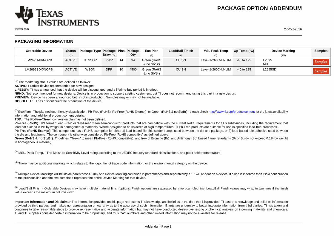
PACKAGING INFORMATION
Orderable Device Status(1)
Package Type PackageDrawing
Pins PackageQty
Eco Plan(2)
Lead/Ball Finish(6)
MSL Peak Temp(3)
Op Temp (°C) Device Marking(4/5)
Samples
LM2695MH/NOPB ACTIVE HTSSOP PWP 14 94 Green (RoHS& no Sb/Br)
CU SN Level-1-260C-UNLIM -40 to 125 L2695MH
LM2695SDX/NOPB ACTIVE WSON DPR 10 4500 Green (RoHS& no Sb/Br)
CU SN Level-1-260C-UNLIM -40 to 125 L2695SD
(1) The marketing status values are defined as follows:ACTIVE: Product device recommended for new designs.LIFEBUY: TI has announced that the device will be discontinued, and a lifetime-buy period is in effect.NRND: Not recommended for new designs. Device is in production to support existing customers, but TI does not recommend using this part in a new design.PREVIEW: Device has been announced but is not in production. Samples may or may not be available.OBSOLETE: TI has discontinued the production of the device.
(2) Eco Plan - The planned eco-friendly classification: Pb-Free (RoHS), Pb-Free (RoHS Exempt), or Green (RoHS & no Sb/Br) - please check http://www.ti.com/productcontent for the latest availabilityinformation and additional product content details.TBD: The Pb-Free/Green conversion plan has not been defined.Pb-Free (RoHS): TI's terms "Lead-Free" or "Pb-Free" mean semiconductor products that are compatible with the current RoHS requirements for all 6 substances, including the requirement thatlead not exceed 0.1% by weight in homogeneous materials. Where designed to be soldered at high temperatures, TI Pb-Free products are suitable for use in specified lead-free processes.Pb-Free (RoHS Exempt): This component has a RoHS exemption for either 1) lead-based flip-chip solder bumps used between the die and package, or 2) lead-based die adhesive used betweenthe die and leadframe. The component is otherwise considered Pb-Free (RoHS compatible) as defined above.Green (RoHS & no Sb/Br): TI defines "Green" to mean Pb-Free (RoHS compatible), and free of Bromine (Br) and Antimony (Sb) based flame retardants (Br or Sb do not exceed 0.1% by weightin homogeneous material)
(3) MSL, Peak Temp. - The Moisture Sensitivity Level rating according to the JEDEC industry standard classifications, and peak solder temperature.
(4) There may be additional marking, which relates to the logo, the lot trace code information, or the environmental category on the device.
(5) Multiple Device Markings will be inside parentheses. Only one Device Marking contained in parentheses and separated by a "~" will appear on a device. If a line is indented then it is a continuationof the previous line and the two combined represent the entire Device Marking for that device.
(6) Lead/Ball Finish - Orderable Devices may have multiple material finish options. Finish options are separated by a vertical ruled line. Lead/Ball Finish values may wrap to two lines if the finishvalue exceeds the maximum column width.
Important Information and Disclaimer:The information provided on this page represents TI's knowledge and belief as of the date that it is provided. TI bases its knowledge and belief on informationprovided by third parties, and makes no representation or warranty as to the accuracy of such information. Efforts are underway to better integrate information from third parties. TI has taken andcontinues to take reasonable steps to provide representative and accurate information but may not have conducted destructive testing or chemical analysis on incoming materials and chemicals.TI and TI suppliers consider certain information to be proprietary, and thus CAS numbers and other limited information may not be available for release.

PACKAGE OPTION ADDENDUM
www.ti.com 27-Oct-2016
Addendum-Page 2
In no event shall TI's liability arising out of such information exceed the total purchase price of the TI part(s) at issue in this document sold by TI to Customer on an annual basis.

TAPE AND REEL INFORMATION
*All dimensions are nominal
Device PackageType
PackageDrawing
Pins SPQ ReelDiameter
(mm)
ReelWidth
W1 (mm)
A0(mm)
B0(mm)
K0(mm)
P1(mm)
W(mm)
Pin1Quadrant
LM2695SDX/NOPB WSON DPR 10 4500 330.0 12.4 4.3 4.3 1.3 8.0 12.0 Q1
PACKAGE MATERIALS INFORMATION
www.ti.com 1-Oct-2016
Pack Materials-Page 1
*All dimensions are nominal
Device Package Type Package Drawing Pins SPQ Length (mm) Width (mm) Height (mm)
LM2695SDX/NOPB WSON DPR 10 4500 367.0 367.0 35.0
PACKAGE MATERIALS INFORMATION
www.ti.com 1-Oct-2016
Pack Materials-Page 2
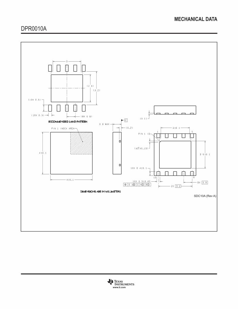
MECHANICAL DATA
DPR0010A
www.ti.com
SDC10A (Rev A)

MECHANICAL DATA
PWP0014A
www.ti.com
MXA14A (Rev A)

IMPORTANT NOTICE
Texas Instruments Incorporated and its subsidiaries (TI) reserve the right to make corrections, enhancements, improvements and otherchanges to its semiconductor products and services per JESD46, latest issue, and to discontinue any product or service per JESD48, latestissue. Buyers should obtain the latest relevant information before placing orders and should verify that such information is current andcomplete. All semiconductor products (also referred to herein as “components”) are sold subject to TI’s terms and conditions of salesupplied at the time of order acknowledgment.TI warrants performance of its components to the specifications applicable at the time of sale, in accordance with the warranty in TI’s termsand conditions of sale of semiconductor products. Testing and other quality control techniques are used to the extent TI deems necessaryto support this warranty. Except where mandated by applicable law, testing of all parameters of each component is not necessarilyperformed.TI assumes no liability for applications assistance or the design of Buyers’ products. Buyers are responsible for their products andapplications using TI components. To minimize the risks associated with Buyers’ products and applications, Buyers should provideadequate design and operating safeguards.TI does not warrant or represent that any license, either express or implied, is granted under any patent right, copyright, mask work right, orother intellectual property right relating to any combination, machine, or process in which TI components or services are used. Informationpublished by TI regarding third-party products or services does not constitute a license to use such products or services or a warranty orendorsement thereof. Use of such information may require a license from a third party under the patents or other intellectual property of thethird party, or a license from TI under the patents or other intellectual property of TI.Reproduction of significant portions of TI information in TI data books or data sheets is permissible only if reproduction is without alterationand is accompanied by all associated warranties, conditions, limitations, and notices. TI is not responsible or liable for such altereddocumentation. Information of third parties may be subject to additional restrictions.Resale of TI components or services with statements different from or beyond the parameters stated by TI for that component or servicevoids all express and any implied warranties for the associated TI component or service and is an unfair and deceptive business practice.TI is not responsible or liable for any such statements.Buyer acknowledges and agrees that it is solely responsible for compliance with all legal, regulatory and safety-related requirementsconcerning its products, and any use of TI components in its applications, notwithstanding any applications-related information or supportthat may be provided by TI. Buyer represents and agrees that it has all the necessary expertise to create and implement safeguards whichanticipate dangerous consequences of failures, monitor failures and their consequences, lessen the likelihood of failures that might causeharm and take appropriate remedial actions. Buyer will fully indemnify TI and its representatives against any damages arising out of the useof any TI components in safety-critical applications.In some cases, TI components may be promoted specifically to facilitate safety-related applications. With such components, TI’s goal is tohelp enable customers to design and create their own end-product solutions that meet applicable functional safety standards andrequirements. Nonetheless, such components are subject to these terms.No TI components are authorized for use in FDA Class III (or similar life-critical medical equipment) unless authorized officers of the partieshave executed a special agreement specifically governing such use.Only those TI components which TI has specifically designated as military grade or “enhanced plastic” are designed and intended for use inmilitary/aerospace applications or environments. Buyer acknowledges and agrees that any military or aerospace use of TI componentswhich have not been so designated is solely at the Buyer's risk, and that Buyer is solely responsible for compliance with all legal andregulatory requirements in connection with such use.TI has specifically designated certain components as meeting ISO/TS16949 requirements, mainly for automotive use. In any case of use ofnon-designated products, TI will not be responsible for any failure to meet ISO/TS16949.
Products ApplicationsAudio www.ti.com/audio Automotive and Transportation www.ti.com/automotiveAmplifiers amplifier.ti.com Communications and Telecom www.ti.com/communicationsData Converters dataconverter.ti.com Computers and Peripherals www.ti.com/computersDLP® Products www.dlp.com Consumer Electronics www.ti.com/consumer-appsDSP dsp.ti.com Energy and Lighting www.ti.com/energyClocks and Timers www.ti.com/clocks Industrial www.ti.com/industrialInterface interface.ti.com Medical www.ti.com/medicalLogic logic.ti.com Security www.ti.com/securityPower Mgmt power.ti.com Space, Avionics and Defense www.ti.com/space-avionics-defenseMicrocontrollers microcontroller.ti.com Video and Imaging www.ti.com/videoRFID www.ti-rfid.comOMAP Applications Processors www.ti.com/omap TI E2E Community e2e.ti.comWireless Connectivity www.ti.com/wirelessconnectivity
Mailing Address: Texas Instruments, Post Office Box 655303, Dallas, Texas 75265Copyright © 2016, Texas Instruments Incorporated
![Data Sheet - RS Components · 2019. 10. 17. · 2 Package Dimensions Absolute Maximum Ratings Supply Voltage, VDD to Ground[1]-0.3 V to 7.0 V Operating Voltage, VDD to Ground[2] 5.5](https://img.dokumen.tips/doc/110x75/6078d6892678e0607178fc1e/data-sheet-rs-components-2019-10-17-2-package-dimensions-absolute-maximum.jpg)