Embed Size (px)
Citation preview

1
10
2
3
4
13
15
5
14
9
7
8
20
19
18
17
16
6
12
11
VCC
BLON
GD1
GD2
GND
CL
CREF
VREF
DSR
DIM
DTY
DADJ
FMIN
FMAX
SS
ICOMP
CS
LEDSW
OV
UV
20 V to 9.5 V
+±
+±
+±
LED String 1
LED String 2
LED String N
VINT1
T2
TN
ON/OFF
DIM PWM Output
UCC25710
Copyright © 2016, Texas Instruments Incorporated
0 100
Dimming Duty Cycle -%
80
95
100
10
85
90
Eff
icie
ncy
- %
-4
2
4
-2
0
Lin
eari
ty E
rro
r -
%
Linearity
Efficiency
Product
Folder
Sample &Buy
Technical
Documents
Tools &
Software
Support &Community
ReferenceDesign
An IMPORTANT NOTICE at the end of this data sheet addresses availability, warranty, changes, use in safety-critical applications,intellectual property matters and other important disclaimers. PRODUCTION DATA.
UCC25710SLUSAD7B –APRIL 2011–REVISED JULY 2016
UCC25710 LLC Half-Bridge Controller For Multi-String LED Lighting
1
1 Features1• Closed-Loop LED String Current Control• PWM Dimming Input• Adjustable FMIN (3% accuracy), and FMAX (7.5%
Accuracy)• LLC and Series LED Switch Control for Dimming• Programmable Dimming LLC ON/OFF Ramp for
Elimination of Audible Noise• Closed-Loop Current Control at Low Dimming
Duty Cycles• Programmable Soft Start• Accurate VREF for Tight Output Regulation• Overvoltage, Undervoltage and Input Overcurrent
Protection With Auto-Restart Response• Second Overcurrent Threshold With Latch-Off
Response• 400-mA/-800-mA Gate Drive Current• Low Start-Up and Operating Currents• Lead (Pb)-Free, 20-Pin, SOIC Package
2 Applications• LED Backlight for LCD TV and Monitors• LED General Lighting
SPACE
3 DescriptionThe UCC25710 device is an LLC half-bridgecontroller for accurate control of multi-string LEDbacklight applications. It is optimized for multi-transformer, multi-string LED architectures. SuperiorLED current matching in multiple strings can beachieved with this controller and architecture.Compared to existing LED backlight solutions, themulti-transformer architecture provides the highestoverall efficiency from AC input to LED load.
The LLC controller function includes a VoltageControlled Oscillator (VCO) with programmable FMINand FMAX, half-bridge gate drivers with a fixed deadtime of 500 ns and a GM current amplifier. The LLCpower delivery is modulated by the controller’s VCOfrequency. The VCO has an accurate andprogrammable frequency range. At very low powerlevels the VCO frequency goes from FMAX to zero tomaximize efficiency at low LED currents.
Device Information(1)
PART NUMBER PACKAGE BODY SIZE (NOM)UCC25710 SOIC (20) 12.80 mm × 7.50 mm
(1) For all available packages, see the orderable addendum atthe end of the data sheet.
Simplified Application DiagramEfficiency and Linearity Results (Dual 45-W
Strings)

2
UCC25710SLUSAD7B –APRIL 2011–REVISED JULY 2016 www.ti.com
Product Folder Links: UCC25710
Submit Documentation Feedback Copyright © 2011–2016, Texas Instruments Incorporated
Table of Contents1 Features .................................................................. 12 Applications ........................................................... 13 Description ............................................................. 14 Revision History..................................................... 25 Description (continued)......................................... 36 Pin Configuration and Functions ......................... 47 Specifications......................................................... 6
7.1 Absolute Maximum Ratings ...................................... 67.2 ESD Ratings.............................................................. 67.3 Recommended Operating Conditions....................... 67.4 Thermal Information .................................................. 77.5 Electrical Characteristics........................................... 77.6 Typical Characteristics ............................................ 10
8 Detailed Description ............................................ 138.1 Overview ................................................................. 138.2 Functional Block Diagram ....................................... 14
8.3 Feature Description................................................. 158.4 Device Functional Modes........................................ 19
9 Application and Implementation ........................ 209.1 Application Information............................................ 209.2 Typical Application ................................................. 20
10 Power Supply Recommendations ..................... 3111 Layout................................................................... 31
11.1 Layout Guidelines ................................................. 3111.2 Layout Example .................................................... 32
12 Device and Documentation Support ................. 3312.1 Receiving Notification of Documentation Updates 3312.2 Community Resource............................................ 3312.3 Trademarks ........................................................... 3312.4 Electrostatic Discharge Caution............................ 3312.5 Glossary ................................................................ 33
13 Mechanical, Packaging, and OrderableInformation ........................................................... 33
4 Revision HistoryNOTE: Page numbers for previous revisions may differ from page numbers in the current version.
Changes from Revision A (May 2011) to Revision B Page
• Added ESD Ratings table, Feature Description section, Device Functional Modes, Application and Implementationsection, Power Supply Recommendations section, Layout section, Device and Documentation Support section, andMechanical, Packaging, and Orderable Information section ................................................................................................. 1
3
UCC25710www.ti.com SLUSAD7B –APRIL 2011–REVISED JULY 2016
Product Folder Links: UCC25710
Submit Documentation FeedbackCopyright © 2011–2016, Texas Instruments Incorporated
5 Description (continued)The LED current loop reference is set by a divider off the VREF 5-V output. The reference can be varied over a0.5-V to 2.6-V range, allowing analog dimming to be combined with PWM dimming.
PWM dimming is used to control an external LED series switch and also to gate on and off the LLC power stage.The LEDSW output along with a simple drive circuit is used to switch on and off the LED string current. Thisoutput responds directly to the input signal at the dimming input, DIM. The LLC is also ramped on and off withthe dimming PWM input. The on and off LLC dimming edges are ramped at programmable slew rates to controlaudible noise. The dimming function includes duty-cycle compensation to allow optimization of overall efficiencyand dimming linearity over a maximum range.
The control voltage to the VCO is set by ICOMP (current amplifier output) during LED ON-times. During start-upthe soft-start pin, SS, controls the VCO response until it exceeds ICOMP. During dimming the rise and fall ratesof the VCO input are controlled by the voltage at the dimming slew rate, DSR, pin while the pedestal of VCOcontrol level continues to be controlled by ICOMP. The current amplifier output is connected to ICOMP onlyduring the commanded dimming LED ON-time. The LLC on-time is extended beyond the LED current ON-time atlow dimming duty-cycles to maintain closed-loop control of the LED current.
Protection thresholds for LED string overvoltage and undervoltage conditions are set with external resistivedividers and accurate internal thresholds. Input current to the converter is monitored with both a restart and latch-off response depending on the overcurrent level. The controller also includes thermal shutdown protection.
The auto restart response to any fault includes a 10-ms reset period followed by a soft start. In the case of asevere input overcurrent, restart is disabled until the input supply is cycled through its UVLO threshold.

1
2
3
4
5
6
7
8
20
19
18
17
16
15
14
13
VCC FMIN
GD1 FMAX
GD2 SS
GND ICOMP
VREF CS
LEDSW CREF
DTY DSR
DADJ CL
9
10
12
11
DIM OV
BLON UV
4
UCC25710SLUSAD7B –APRIL 2011–REVISED JULY 2016 www.ti.com
Product Folder Links: UCC25710
Submit Documentation Feedback Copyright © 2011–2016, Texas Instruments Incorporated
6 Pin Configuration and Functions
DW Package20-Pin SOIC
Top View
Pin FunctionsPIN
TYPE DESCRIPTIONNO. NAME
1 VCC P
Connect a DC power voltage to VCC. Bypass VCC to GND with a 0.47-µF or larger ceramiccapacitor using short PC-board traces. VCC directly supplies power to the gate drivers andVREF which biases all circuit blocks in the UCC25710. Undervoltage lockout (UVLO)comparator prevents operation until VCC rises above VVCCON.
2, 3 GD1&2 OGate drive outputs operate 180° out of phase with a fixed 500 ns of dead time. They typicallydrive either primary end of a gate drive transformer. At start-up or during a fault recovery,initiating the LLC converter begins with GD2 turning on first.
4 GND PThe ground pin is both the reference pin for the controller and the low-side return for the gatedrive signals. Take special care to return all AC decoupling as close as possible to this pinand avoid any common trace length with analog signal return paths.
5 VREF OThe internal 5-V supply and reference rail is brought out to this pin. A small decouplingcapacitor to ground of 1 µF is required. VREF can support up to 10-mA current external tothe device. VREF is enabled when VCC is above VVCCON and BLON is above VBLON.
6 LEDSW O
The LED switch output is a control signal to a series LED switch. This output is low during alow level at the DIM input and whenever the LLC converter is disabled. PWM dimming isdisabled during soft start, and the LEDSW output is high independent of the DIM input. Asimple gate drive circuit is generally required at this output to drive the external FET.
7 DTY I/OThe duty-cycle pin is averaged with a capacitor to ground to form a 1-D proportional voltagethat is compared to the DADJ saw tooth voltage. The average voltage at this pin is 2.5 V(1-D)+0.1 V, where D is the dimming PWM duty-cycle the DIM input.
8 DADJ I/O
A capacitor to ground at the duty-cycle adjust input sets the positive slope of a saw toothwaveform that is compared to a voltage proportional to 1-D where D is the dimming PWMduty-cycle of the DIM input. At the falling edge of the DIM input this comparison is used toextend the LLC ON-time beyond the ON-time of the LED series switch.
9 DIM I
A PWM input signal at the dimming pin controls the average load current by cycling on andoff both an external series LED switch and the gate drives to the LLC converter. A high onthis pin corresponds to an ON condition. The controller ignores a low condition at this inputduring start-up or fault recovery until after the completion of a soft-start sequence.
10 BLON IBacklight ON is an enable signal for the control device. The signal is active high with athreshold of approx 1.2 V. The 5-V reference (VREF) is enabled with BLON which is the biassupply for many of the internal blocks of the device.
5
UCC25710www.ti.com SLUSAD7B –APRIL 2011–REVISED JULY 2016
Product Folder Links: UCC25710
Submit Documentation FeedbackCopyright © 2011–2016, Texas Instruments Incorporated
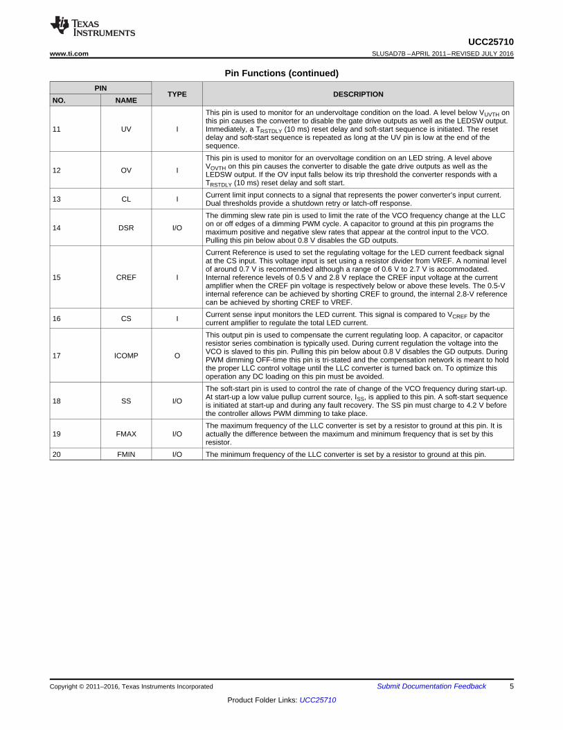
Pin Functions (continued)PIN
TYPE DESCRIPTIONNO. NAME
11 UV I
This pin is used to monitor for an undervoltage condition on the load. A level below VUVTH onthis pin causes the converter to disable the gate drive outputs as well as the LEDSW output.Immediately, a TRSTDLY (10 ms) reset delay and soft-start sequence is initiated. The resetdelay and soft-start sequence is repeated as long at the UV pin is low at the end of thesequence.
12 OV I
This pin is used to monitor for an overvoltage condition on an LED string. A level aboveVOVTH on this pin causes the converter to disable the gate drive outputs as well as theLEDSW output. If the OV input falls below its trip threshold the converter responds with aTRSTDLY (10 ms) reset delay and soft start.
13 CL I Current limit input connects to a signal that represents the power converter’s input current.Dual thresholds provide a shutdown retry or latch-off response.
14 DSR I/O
The dimming slew rate pin is used to limit the rate of the VCO frequency change at the LLCon or off edges of a dimming PWM cycle. A capacitor to ground at this pin programs themaximum positive and negative slew rates that appear at the control input to the VCO.Pulling this pin below about 0.8 V disables the GD outputs.
15 CREF I
Current Reference is used to set the regulating voltage for the LED current feedback signalat the CS input. This voltage input is set using a resistor divider from VREF. A nominal levelof around 0.7 V is recommended although a range of 0.6 V to 2.7 V is accommodated.Internal reference levels of 0.5 V and 2.8 V replace the CREF input voltage at the currentamplifier when the CREF pin voltage is respectively below or above these levels. The 0.5-Vinternal reference can be achieved by shorting CREF to ground, the internal 2.8-V referencecan be achieved by shorting CREF to VREF.
16 CS I Current sense input monitors the LED current. This signal is compared to VCREF by thecurrent amplifier to regulate the total LED current.
17 ICOMP O
This output pin is used to compensate the current regulating loop. A capacitor, or capacitorresistor series combination is typically used. During current regulation the voltage into theVCO is slaved to this pin. Pulling this pin below about 0.8 V disables the GD outputs. DuringPWM dimming OFF-time this pin is tri-stated and the compensation network is meant to holdthe proper LLC control voltage until the LLC converter is turned back on. To optimize thisoperation any DC loading on this pin must be avoided.
18 SS I/O
The soft-start pin is used to control the rate of change of the VCO frequency during start-up.At start-up a low value pullup current source, ISS, is applied to this pin. A soft-start sequenceis initiated at start-up and during any fault recovery. The SS pin must charge to 4.2 V beforethe controller allows PWM dimming to take place.
19 FMAX I/OThe maximum frequency of the LLC converter is set by a resistor to ground at this pin. It isactually the difference between the maximum and minimum frequency that is set by thisresistor.
20 FMIN I/O The minimum frequency of the LLC converter is set by a resistor to ground at this pin.
6
UCC25710SLUSAD7B –APRIL 2011–REVISED JULY 2016 www.ti.com
Product Folder Links: UCC25710
Submit Documentation Feedback Copyright © 2011–2016, Texas Instruments Incorporated
(1) Stresses beyond those listed under Absolute Maximum Ratings may cause permanent damage to the device. These are stress ratingsonly, which do not imply functional operation of the device at these or any other conditions beyond those indicated under RecommendedOperating Conditions. Exposure to absolute-maximum-rated conditions for extended periods may affect device reliability.
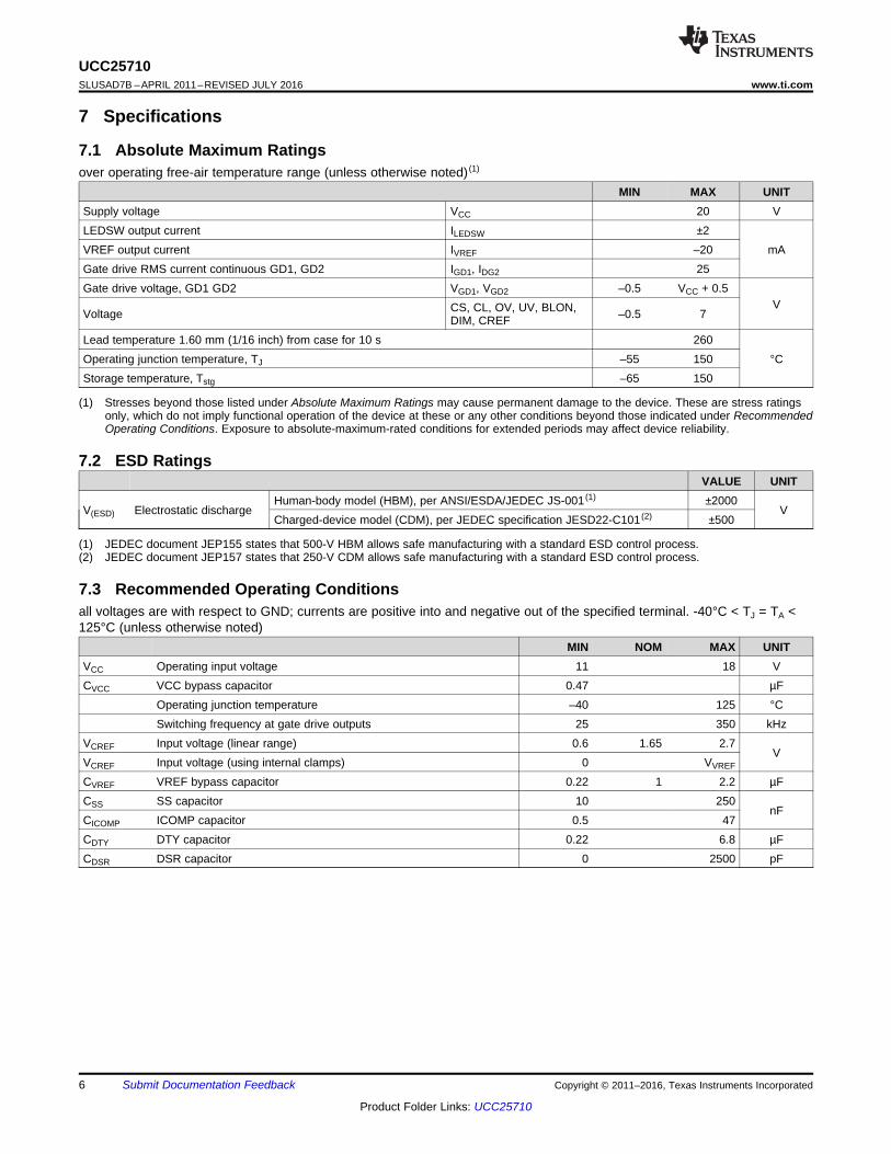
7 Specifications
7.1 Absolute Maximum Ratingsover operating free-air temperature range (unless otherwise noted) (1)
MIN MAX UNITSupply voltage VCC 20 VLEDSW output current ILEDSW ±2
mAVREF output current IVREF –20Gate drive RMS current continuous GD1, GD2 IGD1, IDG2 25Gate drive voltage, GD1 GD2 VGD1, VGD2 –0.5 VCC + 0.5
VVoltage CS, CL, OV, UV, BLON,
DIM, CREF –0.5 7
Lead temperature 1.60 mm (1/16 inch) from case for 10 s 260°COperating junction temperature, TJ –55 150
Storage temperature, Tstg –65 150
(1) JEDEC document JEP155 states that 500-V HBM allows safe manufacturing with a standard ESD control process.(2) JEDEC document JEP157 states that 250-V CDM allows safe manufacturing with a standard ESD control process.
7.2 ESD RatingsVALUE UNIT
V(ESD) Electrostatic dischargeHuman-body model (HBM), per ANSI/ESDA/JEDEC JS-001 (1) ±2000
VCharged-device model (CDM), per JEDEC specification JESD22-C101 (2) ±500
7.3 Recommended Operating Conditionsall voltages are with respect to GND; currents are positive into and negative out of the specified terminal. -40°C < TJ = TA <125°C (unless otherwise noted)
MIN NOM MAX UNITVCC Operating input voltage 11 18 VCVCC VCC bypass capacitor 0.47 µF
Operating junction temperature –40 125 °CSwitching frequency at gate drive outputs 25 350 kHz
VCREF Input voltage (linear range) 0.6 1.65 2.7V
VCREF Input voltage (using internal clamps) 0 VVREF
CVREF VREF bypass capacitor 0.22 1 2.2 µFCSS SS capacitor 10 250
nFCICOMP ICOMP capacitor 0.5 47CDTY DTY capacitor 0.22 6.8 µFCDSR DSR capacitor 0 2500 pF
7
UCC25710www.ti.com SLUSAD7B –APRIL 2011–REVISED JULY 2016
Product Folder Links: UCC25710
Submit Documentation FeedbackCopyright © 2011–2016, Texas Instruments Incorporated
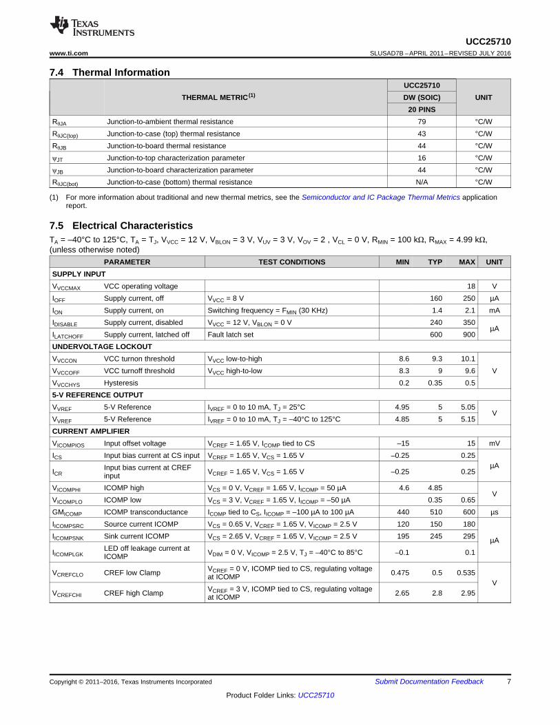
(1) For more information about traditional and new thermal metrics, see the Semiconductor and IC Package Thermal Metrics applicationreport.
7.4 Thermal Information
THERMAL METRIC (1)UCC25710
UNITDW (SOIC)20 PINS
RθJA Junction-to-ambient thermal resistance 79 °C/WRθJC(top) Junction-to-case (top) thermal resistance 43 °C/WRθJB Junction-to-board thermal resistance 44 °C/WψJT Junction-to-top characterization parameter 16 °C/WψJB Junction-to-board characterization parameter 44 °C/WRθJC(bot) Junction-to-case (bottom) thermal resistance N/A °C/W
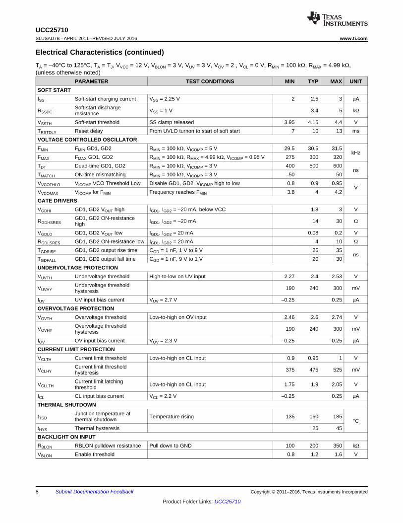
7.5 Electrical CharacteristicsTA = –40°C to 125°C, TA = TJ, VVCC = 12 V, VBLON = 3 V, VUV = 3 V, VOV = 2 , VCL = 0 V, RMIN = 100 kΩ, RMAX = 4.99 kΩ,(unless otherwise noted)
PARAMETER TEST CONDITIONS MIN TYP MAX UNITSUPPLY INPUTVVCCMAX VCC operating voltage 18 VIOFF Supply current, off VVCC = 8 V 160 250 µAION Supply current, on Switching frequency = FMIN (30 KHz) 1.4 2.1 mAIDISABLE Supply current, disabled VVCC = 12 V, VBLON = 0 V 240 350
µAILATCHOFF Supply current, latched off Fault latch set 600 900UNDERVOLTAGE LOCKOUTVVCCON VCC turnon threshold VVCC low-to-high 8.6 9.3 10.1
VVVCCOFF VCC turnoff threshold VVCC high-to-low 8.3 9 9.6VVCCHYS Hysteresis 0.2 0.35 0.55-V REFERENCE OUTPUTVVREF 5-V Reference IVREF = 0 to 10 mA, TJ = 25°C 4.95 5 5.05
VVVREF 5-V Reference IVREF = 0 to 10 mA, TJ = –40°C to 125°C 4.85 5 5.15CURRENT AMPLIFIERVICOMPIOS Input offset voltage VCREF = 1.65 V, ICOMP tied to CS –15 15 mVICS Input bias current at CS input VCREF = 1.65 V, VCS = 1.65 V –0.25 0.25
µAICR
Input bias current at CREFinput VCREF = 1.65 V, VCS = 1.65 V –0.25 0.25
VICOMPHI ICOMP high VCS = 0 V, VCREF = 1.65 V, IICOMP = 50 µA 4.6 4.85V
VICOMPLO ICOMP low VCS = 3 V, VCREF = 1.65 V, IICOMP = –50 µA 0.35 0.65GMICOMP ICOMP transconductance ICOMP tied to CS, IICOMP = –100 µA to 100 µA 440 510 600 µsIICOMPSRC Source current ICOMP VCS = 0.65 V, VCREF = 1.65 V, VICOMP = 2.5 V 120 150 180
µAIICOMPSNK Sink current ICOMP VCS = 2.65 V, VCREF = 1.65 V, VICOMP = 2.5 V 195 245 295
IICOMPLGKLED off leakage current atICOMP VDIM = 0 V, VICOMP = 2.5 V, TJ = –40°C to 85°C –0.1 0.1
VCREFCLO CREF low Clamp VCREF = 0 V, ICOMP tied to CS, regulating voltageat ICOMP 0.475 0.5 0.535
VVCREFCHI CREF high Clamp VCREF = 3 V, ICOMP tied to CS, regulating voltage
at ICOMP 2.65 2.8 2.95
8
UCC25710SLUSAD7B –APRIL 2011–REVISED JULY 2016 www.ti.com
Product Folder Links: UCC25710
Submit Documentation Feedback Copyright © 2011–2016, Texas Instruments Incorporated
Electrical Characteristics (continued)TA = –40°C to 125°C, TA = TJ, VVCC = 12 V, VBLON = 3 V, VUV = 3 V, VOV = 2 , VCL = 0 V, RMIN = 100 kΩ, RMAX = 4.99 kΩ,(unless otherwise noted)
PARAMETER TEST CONDITIONS MIN TYP MAX UNITSOFT STARTISS Soft-start charging current VSS = 2.25 V 2 2.5 3 µA
RSSDCSoft-start dischargeresistance VSS = 1 V 3.4 5 kΩ
VSSTH Soft-start threshold SS clamp released 3.95 4.15 4.4 VTRSTDLY Reset delay From UVLO turnon to start of soft start 7 10 13 msVOLTAGE CONTROLLED OSCILLATORFMIN FMIN GD1, GD2 RMIN = 100 kΩ, VICOMP = 5 V 29.5 30.5 31.5
kHzFMAX FMAX GD1, GD2 RMIN = 100 kΩ, RMAX = 4.99 kΩ, VICOMP = 0.95 V 275 300 320TDT Dead-time GD1, GD2 RMIN = 100 kΩ, VICOMP = 3 V 400 500 600
nsTMATCH ON-time mismatching RMIN = 100 kΩ, VICOMP = 3 V –50 50VVCOTHLO VICOMP VCO Threshold Low Disable GD1, GD2, VICOMP high to low 0.8 0.9 0.95
VVVCOMAX VICOMP for FMIN Frequency reaches FMIN 3.8 4 4.2GATE DRIVERSVGDHI GD1, GD2 VOUT high IGD1, IGD2 = –20 mA, below VCC 1.8 3 V
RGDHSRESGD1, GD2 ON-resistancehigh IGD1, IGD2 = –20 mA 14 30 Ω
VGDLO GD1, GD2 VOUT low IGD1, IGD2 = 20 mA 0.08 0.2 VRGDLSRES GD1, GD2 ON-resistance low IGD1, IGD2 = 20 mA 4 10 Ω
TGDRISE GD1, GD2 output rise time CGD = 1 nF, 1 V to 9 V 25 35ns
TGDFALL GD1, GD2 output fall time CGD = 1 nF, 9 V to 1 V 20 30UNDERVOLTAGE PROTECTIONVUVTH Undervoltage threshold High-to-low on UV input 2.27 2.4 2.53 V
VUVHYUndervoltage thresholdhysteresis 190 240 300 mV
IUV UV input bias current VUV = 2.7 V –0.25 0.25 µAOVERVOLTAGE PROTECTIONVOVTH Overvoltage threshold Low-to-high on OV input 2.46 2.6 2.74 V
VOVHYOvervoltage thresholdhysteresis 190 240 300 mV
IOV OV input bias current VOV = 2.3 V –0.25 0.25 µACURRENT LIMIT PROTECTIONVCLTH Current limit threshold Low-to-high on CL input 0.9 0.95 1 V
VCLHYCurrent limit thresholdhysteresis 375 475 525 mV
VCLLTHCurrent limit latchingthreshold Low-to-high on CL input 1.75 1.9 2.05 V
ICL CL input bias current VCL = 2.2 V –0.25 0.25 µATHERMAL SHUTDOWN
tTSDJunction temperature atthermal shutdown Temperature rising 135 160 185
°CtHYS Thermal hysteresis 25 45BACKLIGHT ON INPUTRBLON RBLON pulldown resistance Pull down to GND 100 200 350 kΩVBLON Enable threshold 0.8 1.2 1.6 V
9
UCC25710www.ti.com SLUSAD7B –APRIL 2011–REVISED JULY 2016
Product Folder Links: UCC25710
Submit Documentation FeedbackCopyright © 2011–2016, Texas Instruments Incorporated
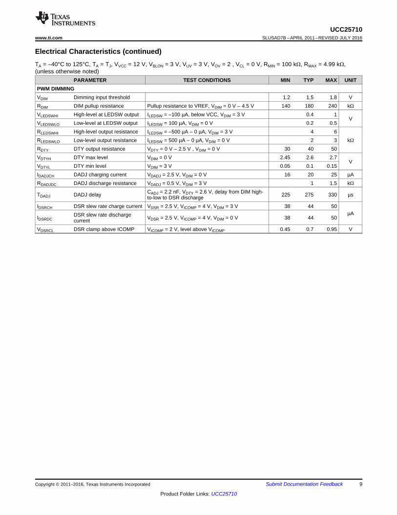
Electrical Characteristics (continued)TA = –40°C to 125°C, TA = TJ, VVCC = 12 V, VBLON = 3 V, VUV = 3 V, VOV = 2 , VCL = 0 V, RMIN = 100 kΩ, RMAX = 4.99 kΩ,(unless otherwise noted)
PARAMETER TEST CONDITIONS MIN TYP MAX UNITPWM DIMMINGVDIM Dimming input threshold 1.2 1.5 1.8 VRDIM DIM pullup resistance Pullup resistance to VREF, VDIM = 0 V – 4.5 V 140 180 240 kΩVLEDSWHI High-level at LEDSW output ILEDSW = –100 µA, below VCC, VDIM = 3 V 0.4 1
VVLEDSWLO Low-level at LEDSW output ILEDSW = 100 µA, VDIM = 0 V 0.2 0.5RLEDSWHI High-level output resistance ILEDSW = –500 µA – 0 µA, VDIM = 3 V 4 6
kΩRLEDSWLO Low-level output resistance ILEDSW = 500 µA – 0 µA, VDIM = 0 V 2 3RDTY DTY output resistance VDTY = 0 V – 2.5 V , VDIM = 0 V 30 40 50VDTYH DTY max level VDIM = 0 V 2.45 2.6 2.7
VVDTYL DTY min level VDIM = 3 V 0.05 0.1 0.15IDADJCH DADJ charging current VDADJ = 2.5 V, VDIM = 0 V 16 20 25 µARDADJDC DADJ discharge resistance VDADJ = 0.5 V, VDIM = 3 V 1 1.5 kΩ
TDADJ DADJ delay CADJ = 2.2 nF, VDTY = 2.6 V, delay from DIM high-to-low to DSR discharge 225 275 330 µs
IDSRCH DSR slew rate charge current VDSR = 2.5 V, VICOMP = 4 V, VDIM = 3 V 38 44 50µA
IDSRDCDSR slew rate dischargecurrent VDSR = 2.5 V, VICOMP = 4 V, VDIM = 0 V 38 44 50
VDSRCL DSR clamp above ICOMP VICOMP = 2 V, level above VICOMP 0.45 0.7 0.95 V

0 5.0
Input Voltage at CS(V)
2.0
Out
putC
urr
entatI C
OM
P(m
A)
1.0 3.0 4.0
100
-300
200
-100
0
-200
300
400
VCREF = 0 V
VCREF = 1 V
VCREF = 1.5 V
VCREF = 2.0 V
VCREF = 5.0 V
Sinking Current
Sourcing Current
-40 140
Temperature (°C)
4.90
5.05
5.10
40
4.95
5.00
VV
RE
FR
efe
ren
ce
Voltage
(V)
200-20 60 80 100 120
-40 140
Temperature (°C)
100
350
400
40
200
250
I DIS
AB
LE
and
I OF
FS
upply
Curr
ent(m
A)
300
150
200-20 60 80 100 120
IOFF
VVCC = 8 V
IDISABLE
VVCC = 12 VVBLON = 0 V
-40 140
Temperature (°C)
1.0
1.8
2.0
40
1.3
1.5
I ON
Supp
lyC
urr
ent
(mA
)
1.7
1.9
1.2
1.4
200-20 60 80 100 120
VVCC = 18 V
VVCC = 12 V
1.6
1.2
Switching Frequency = FMIN
No Gate Drive Load
-40 140
Temperature (°C)
8.5
9.3
9.5
40
8.8
9.0
VV
CC
ON
and
VV
CC
OF
FT
hre
shold
(V)
9.2
9.4
8.6
8.9
200-20 60 80 100 120
9.1
8.7
Falling - VVCCOFF
Rising - VVCCON
0 18
VCC Supply Voltage (V)
0
1.2
1.6
8
0.4
0.8
VC
CS
upply
Curr
ent(m
A)
1.0
1.4
0.2
0.6
642 10 12 14 16
Turn On
Turn Off
Switching Frequency = FMIN
No Gate Drive Load
10
UCC25710SLUSAD7B –APRIL 2011–REVISED JULY 2016 www.ti.com
Product Folder Links: UCC25710
Submit Documentation Feedback Copyright © 2011–2016, Texas Instruments Incorporated
7.6 Typical Characteristics
Figure 1. Supply Current vs Dimming Duty Cycle Figure 2. VVCCON and VVCOFF Threshold vs Temperature
Figure 3. Supply Current vs Temperature Figure 4. IDISABLE and IOFF Supply Current vsTemperature
Figure 5. Reference Voltage vs Temperature Figure 6. Output Current (ICOMP) vs Input Voltage (CS)

-100 300
Time (ns)
100
Gate
Drive
Volta
ge
(V)
0 200
0
10
12
2
6
8
4
0
1.5
1.8
0.9
0.3
1.2
0.6
Gate
Driv
eS
ourc
eC
urr
ent(A
)
TA = 125oC
TA = 25oC
CLOAD = 4.7 nF
RLOAD = 2.5 kW
-100 300
Time (ns)
100
Gate
Drive
Volta
ge
(V)
0 200
0
10
12
2
6
8
4
0
1.5
1.8
0.9
0.3
1.2
0.6
Gate
Drive
Sin
king
Curr
ent(A
)
TA = 125oC
TA = 25oC
CLOAD = 4.7 nF
RLOAD = 2.5 kW
-40 140
Temperature (°C)
40
FM
AX
Sw
itchin
gF
req
uen
cy
(kH
z)
200-20 60 80 100 120
280
320
290
300
285
315
295
305
310
-40 140
Temperature (°C)
40
TD
TG
ate
Dri
ve
Dead
Tim
e(n
s)
200-20 60 80 100 120
400
560
600
440
500
420
580
480
520
540
460
-40 140
Temperature (°C)
40
GM
ICO
MP
Cha
nge
Fro
mV
alu
ea
t25
oC
(%)
200-20 60 80 100 120
-5%
3%
5%
-3%
0
-4%
4%
-1%
1%
2%
-2%
-40 140
Temperature (°C)
29.5
31.1
31.5
40
29.9
30.5
FM
INS
witchin
gF
reque
ncy
(kH
z)
200-20 60 80 100 120
29.7
31.3
30.3
30.7
30.9
30.1
11
UCC25710www.ti.com SLUSAD7B –APRIL 2011–REVISED JULY 2016
Product Folder Links: UCC25710
Submit Documentation FeedbackCopyright © 2011–2016, Texas Instruments Incorporated
Typical Characteristics (continued)
Figure 7. GMICOMP vs Temperature Figure 8. Minimum Switching Frequency vs Temperature
Figure 9. Maximum Switching Frequency vs Temperature Figure 10. Gate Drive Dead Time vs Temperature
Figure 11. Gate Driver Outputs (Rising Edge) vs Time Figure 12. Gate Driver Outputs (Falling Edge) vs Time
-40 140
Temperature (°C)
40
TD
AD
JO
n-T
ime
Exte
nsi
on
(ms)
200-20 60 80 100 120
240
320
260
250
330
280
290
300
270
230
310
CDADJ = 2.2 nF
VDTY = 2.6 V
-1 9
Time (ms)
3
LE
DS
WV
oltage
(V)
210 4 5 7 8
2
12
4
14
8
10
6
0
TA = 125oC
TA = 25oC
CLOAD = 100 pFTA = -40oC
LEDSW Output
DIM Input
6
0 100
Dimming PWM Duty Cycle (%)
40
TD
AD
JO
n-T
ime
Exte
nsi
on
(ms)
20 60 80
50
400
150
100
450
250
300
350
200
0
CDTY = 2.2 mF
Dimming Frequency= 300 Hz
CDADJ 3.3 nF
CDADJ 1.0 nF
CDADJ 330 pF
-40 140
Temperature (°C)
-2%
1%
2%
40
-1%
0
I IDS
RC
H,I ID
SR
DC
Ch
ange
Fro
mV
alu
ea
t25
oC
(%)
200-20 60 80 100 120
Discharge Current
Charge Current
0.5%
1.5%
-1.5%
-0.5%
12
UCC25710SLUSAD7B –APRIL 2011–REVISED JULY 2016 www.ti.com
Product Folder Links: UCC25710
Submit Documentation Feedback Copyright © 2011–2016, Texas Instruments Incorporated
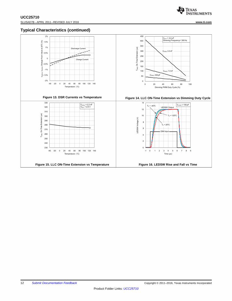
Typical Characteristics (continued)
Figure 13. DSR Currents vs Temperature Figure 14. LLC ON-Time Extension vs Dimming Duty Cycle
Figure 15. LLC ON-Time Extension vs Temperature Figure 16. LEDSW Rise and Fall vs Time

13
UCC25710www.ti.com SLUSAD7B –APRIL 2011–REVISED JULY 2016
Product Folder Links: UCC25710
Submit Documentation FeedbackCopyright © 2011–2016, Texas Instruments Incorporated
8 Detailed Description
8.1 OverviewThe UCC25710 is a highly integrated LLC controller designed specifically for multi-string LED lightingapplications. The half-bridge LLC control is combined with independent PWM dimming or non-dimming of theLED current for control of the light output.
The UCC25710 is designed to provide power from a high voltage DC bus, such as the output from a PFC stage.Input over current-sensing protects the system in the event of a fault and gate drive outputs provide the drivesignals to the LLC stage. Output overvoltage and undervoltage provide additional protection. LED current issensed with a resistor in series with the LED’s. The UCC25710 has separate enable and dimming inputs.
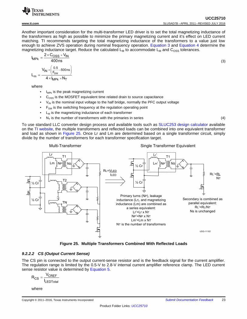
This arrangement of a multi-transformer architecture, as shown in Figure 25, results in a highly efficient powersupply.
1 +VVCCON/VCCOFF
9.3 V/9.0 V
5 V
REF
VVREF
Dead
Tim
e
2
3
4
D Q
QCLR
RESET
20
19
GMICOMP
510 mS
18
UVLO
ISS
2.5 mA
16CS
SS
FMAX
FMIN
GD1
GD2
VCC
VSSTH
4.2 V
6 LEDSW
VVCO
D Q
QCLR
13 CL+
VCLTH
0.95 V/0.475 V
GND
FAULT
GD Toggle
Edge Sync
GD Enable
VCLLTH
1.9 VSQ
Q R UVLO
Latch-Off
+
+ 12 OVVOVTH
2.6 V/2.4 V
11 UV
VUVTH
2.4 V/2.6 VSS-END
SS-END
5VREF
2*F
VVREF
FMIN
FSW
Zero Frequency Command
80 kW
80 kW
2.5 mA
7
8
9
200 kW
DIM
DADJ
DTY
VVREF
LH
Dimming PWM
OFF
ON
200 kW
10BLON
15CREF
VVREF
~4 V
H
LLC-OFF
LED-ON
LED-ON
SS-END
17
H
ICOMP
Soft Start
S Q
QR*
+
+
LLC-OFF
H
L
IDSRCH
44 mA
IDSRDC
44 mA
VVREF
14DSR
VVREF
SS Clamp
DIM ON/OFFCLAMP
1V 4V
VVCO
FMAX
VCOFSW
0.9V
Dimming SlewControl
GND
ICOMP
RST Gen
S*
Q
QRdelay
UCC25710
+
RESET
RESET
TSD
ENBL
Disab le
LATCH -OFFLow ICC
FAULTENBL
+++
VCLREFCLO, 0.5 V
VCLREFCHI, 2.8 V
TRSTDLY
10 ms
IDADJCH
20 mA
4 kW
Current
Amplifier
delay
2.4 ms
14
UCC25710SLUSAD7B –APRIL 2011–REVISED JULY 2016 www.ti.com
Product Folder Links: UCC25710
Submit Documentation Feedback Copyright © 2011–2016, Texas Instruments Incorporated
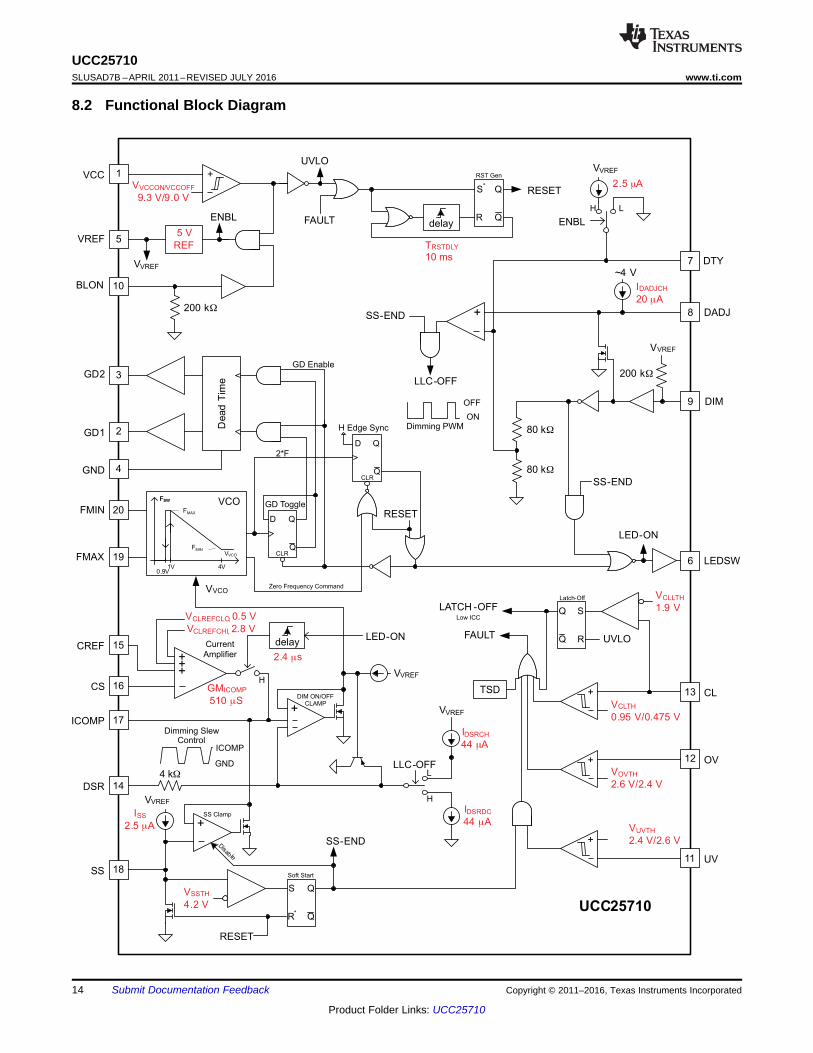
8.2 Functional Block Diagram

15
UCC25710www.ti.com SLUSAD7B –APRIL 2011–REVISED JULY 2016
Product Folder Links: UCC25710
Submit Documentation FeedbackCopyright © 2011–2016, Texas Instruments Incorporated
8.3 Feature DescriptionSignal names and pin functions are depicted in Functional Block Diagram.
8.3.1 Multi-transformer ArchitectureThe multi-transformer LED driver architecture is a very attractive solution for driving multiple LED strings at thesame current using a single power train and control device. Excellent LED string current matching from string tostring (<1%) excellent LED current linearity from 1% to 100% dimming (<2%), and high efficiency can beachieved (>94%). Because this architecture is intended to use the 400-V output of the PFC stage, there is asignificant cost advantage over typical LED backlight implementations because a power stage can be eliminated.
The architecture and UCC25710 control device are based on the LLC resonant half-bridge topology. Thecontroller feedback loop is configured to regulate the total LED current typically with a current-sense resistor. Thearrangement of the transformers with the primaries in series provides excellent LED string current matching.Because the primaries are in series, the current in each transformer primary is the same. The secondary currentis the primary current times the turns ratio. The net primary magnetizing current is circulated in the primary sideof the half bridge and does not affect the current transferred to the outputs. In each transformer, differences inmagnetizing current caused by different magnetizing inductance or winding voltage will cause a difference incurrent transferred to the LED outputs, although the difference in transferred current is minimal with typicaltransformer tolerances and following the guidance in the Determining Transformer and Resonant CircuitParameters below.
The UCC25710 includes all of the functions necessary to implement a total LED backlight driver including GMcurrent amplifier, VCO, reference regulator, soft start, dimming duty cycle compensation and protection for OV,UV, current limit, and thermal shutdown. There are additional features to minimize audible noise during dimmingand provide fast LED current rise and fall times.
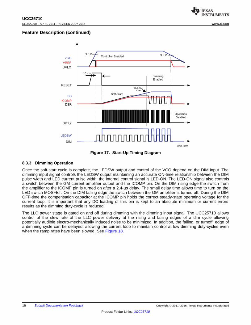
8.3.2 Start-Up and Non-Dimming OperationThe UCC27510 is enabled when VCC exceeds the VVCCON threshold and BLON is high. At this time the soft-startcycle is initiated following a 10-ms reset delay. A 2.5-µA current source charges the capacitor connected to theSS pin to generate the soft-start ramp. During the soft-start cycle the current amplifier output (ICOMP) is clampedto be equal to or less than SS voltage. The voltage on ICOMP controls the VCO. VICOMP achieves the steadystate operating point to regulate the total LED current during the soft-start rise time. The DIM input and the UVinput are disabled during soft start to allow the output capacitors to charge to the steady-state operating voltage.When the SS pin reaches the VSSTH threshold the SS-END signal transitions high indicating the end of the soft-start cycle. At this time the UV comparator and DIM input are enabled. See Figure 17 for the timing relationshipduring soft start.
UDG-11095
9.3 V
10 ms
9.0 V
Dimming
Enabled
Soft-Start
Operation
Disabled
Controller Enabled
Soft-Start
Over
VCC
DIM
SS
DSR
GD1,2
UVLO
RESET
LEDSW
VREF
ICOMP
16
UCC25710SLUSAD7B –APRIL 2011–REVISED JULY 2016 www.ti.com
Product Folder Links: UCC25710
Submit Documentation Feedback Copyright © 2011–2016, Texas Instruments Incorporated
Feature Description (continued)
Figure 17. Start-Up Timing Diagram
8.3.3 Dimming OperationOnce the soft-start cycle is complete, the LEDSW output and control of the VCO depend on the DIM input. Thedimming input signal controls the LEDSW output maintaining an accurate ON-time relationship between the DIMpulse width and LED current pulse width; the internal control signal is LED-ON. The LED-ON signal also controlsa switch between the GM current amplifier output and the ICOMP pin. On the DIM rising edge the switch fromthe amplifier to the ICOMP pin is turned on after a 2.4-µs delay. The small delay time allows time to turn on theLED switch MOSFET. On the DIM falling edge the switch between the GM amplifier is turned off. During the DIMOFF-time the compensation capacitor at the ICOMP pin holds the correct steady-state operating voltage for thecurrent loop. It is important that any DC loading of this pin is kept to an absolute minimum or current errorsresults as the dimming duty-cycle is reduced.
The LLC power stage is gated on and off during dimming with the dimming input signal. The UCC25710 allowscontrol of the slew rate of the LLC power delivery at the rising and falling edges of a dim cycle allowingpotentially audible electro-mechanically induced noise to be minimized. In addition, the falling, or turnoff, edge ofa dimming cycle can be delayed, allowing the current loop to maintain control at low dimming duty-cycles evenwhen the ramp rates have been slowed. See Figure 18.

UDG-11097
1 V 4 V
VVCO
FMAX
FMIN
FSW
0.9 V
GD
1&
2
bo
thlo
wVC
OF
req
ue
ncy
VCO Control Voltage
UDG-11096
DSR
LEDSW
DADJ
DTY
DIMDTY = 0.1V + 2.5V*(1-D)
Added
LLC On-Time
LLC On/Off
Slew Rate
50% Dimming 10% Dimming
IPri
ICOMP
17
UCC25710www.ti.com SLUSAD7B –APRIL 2011–REVISED JULY 2016
Product Folder Links: UCC25710
Submit Documentation FeedbackCopyright © 2011–2016, Texas Instruments Incorporated
Feature Description (continued)
Figure 18. Dimming Timing Diagram
The power through the LLC converter is inversely proportional to the frequency of the VCO. The VCO frequency,in turn, is inversely proportional to the VCO control signal. See Figure 19 for details of this relationship. Thedimming input generates an LLC-OFF signal that is used to select either a charging or discharging state for acapacitor applied to the DSR pin. The ±44 µA of current and associated capacitor set a ramp rate for the rise andfall of the DSR voltage. The control voltage to the VCO is dominated by the DSR voltage when the DSR voltageis less than the ICOMP pin – allowing the falling ramp on the DSR pin to softly turnoff the LLC power stage andsoftly return it to the same operating state as it rises.
Figure 19. VCO Characteristics
The LLC-OFF signal is an inverted version of the dimming input signal. The falling edge of LLC-OFF issynchronized with the rising edge of the DIM signal. At a negative DIM edge the DADJ and DTY signals arecombined to delay the rising edge of LLC-OFF providing a duty-cycle compensation time that is a function of thedimming duty cycle.

UDG-11100
GD1,2
RESET
10 ms
SS
OV, CL,
TSD Fault
18
UCC25710SLUSAD7B –APRIL 2011–REVISED JULY 2016 www.ti.com
Product Folder Links: UCC25710
Submit Documentation Feedback Copyright © 2011–2016, Texas Instruments Incorporated
Feature Description (continued)Averaged by a capacitor at the DTY pin, the voltage on DTY is inversely proportional to the dimming duty cycle;the voltage is
0.1 V + 2.5 V × (1-D)
where• D is the dimming PWM duty-cycle (1)
The DTY voltage range is 100 mV at 100% DIM duty-cycle, or LED current continuously on, to 2.6 V at 0% DIMduty cycle, or LED current continuously off. The DADJ pin 20-µA current source is allowed to charge the pincapacitor after a DIM falling edge. The LLC-OFF signal transitions high when the capacitor on DADJ charges tothe voltage on DTY. See Figure 18 for the timing relationship during dimming. The scope plots in Figure 20 andFigure 21 below show an example LED driver at 10% and 50% DIM duty cycle.
Figure 20. DIM 10% at 300 Hz Figure 21. DIM 50% at 300 Hz
8.3.4 Fault Condition OperationThe UCC25710 has a similar response to overvoltage, thermal shutdown and current limit faults. Figure 22shows the fault response. The OV input has a 2.6-V threshold and 240 mV of hysteresis. When OV is above 2.6V the internal FAULT signal is active which results in the RESET signal going high. With RESET high the gatedrivers are disabled, the SS pin is discharged to ground, and the LEDSW output is turned off. When OV is below2.36 V the FAULT signal is inactive which starts the 10-ms SS clamp timer.
Figure 22. OV, CL(1 V) and TSD Fault Timing Diagram
UV Fault
RESET
SS
LEDSW
GD1, 2
UDG-11101
19
UCC25710www.ti.com SLUSAD7B –APRIL 2011–REVISED JULY 2016
Product Folder Links: UCC25710
Submit Documentation FeedbackCopyright © 2011–2016, Texas Instruments Incorporated
Feature Description (continued)RESET is extended 10 ms beyond FAULT going low. After the 10-ms soft-start timer the normal soft-startsequence begins. Thermal shutdown generates the same internal FAULT signal when the internal temperaturereaches 160°C and a restart sequence begins after the junction temperature drops by the 25°C of thresholdhysteresis.
The current limit comparator has two thresholds. The lower threshold of 0.95 V results in a shutdown and restartas described for OVP, the OC pin has 0.475 V of hysteresis. The second current limit threshold of 1.9 V resultsin a latch-off fault. VCC must be recycled below the VCCOFF threshold to reset the latched OC fault.
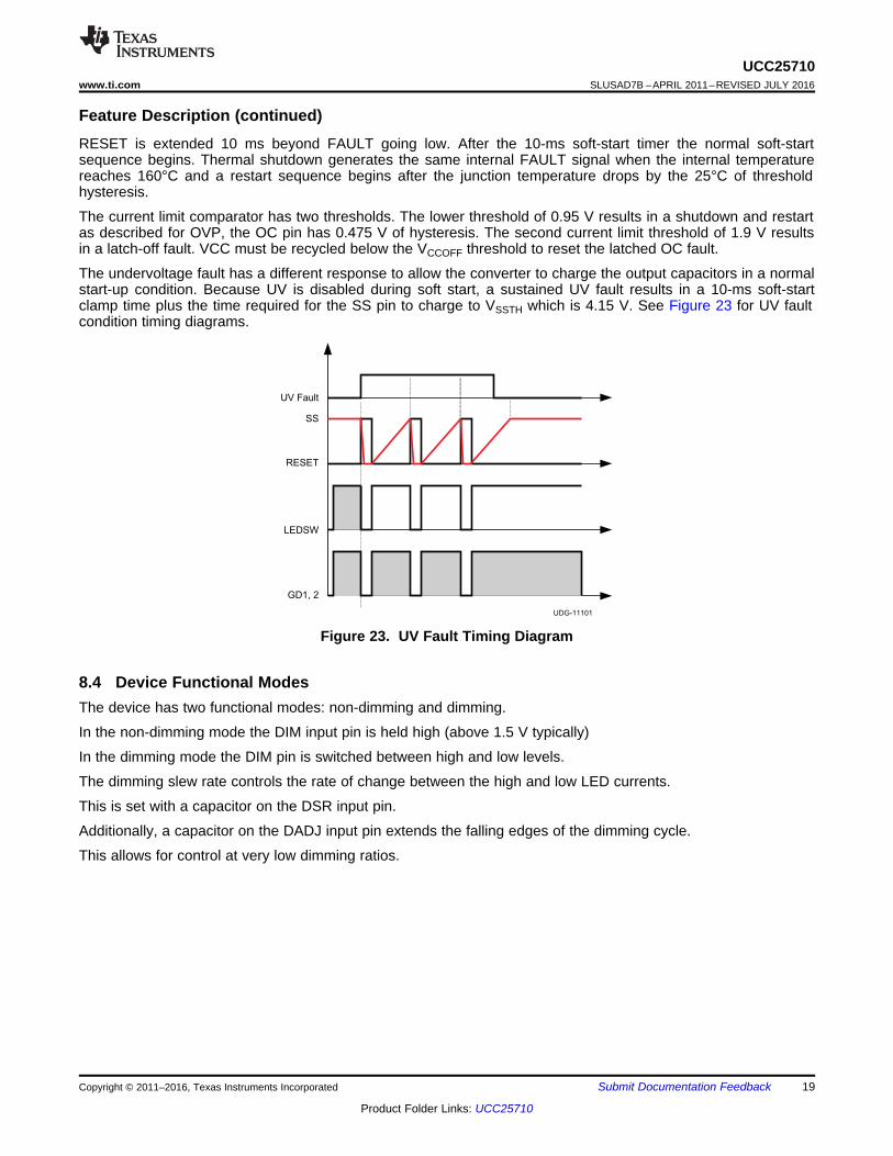
The undervoltage fault has a different response to allow the converter to charge the output capacitors in a normalstart-up condition. Because UV is disabled during soft start, a sustained UV fault results in a 10-ms soft-startclamp time plus the time required for the SS pin to charge to VSSTH which is 4.15 V. See Figure 23 for UV faultcondition timing diagrams.
Figure 23. UV Fault Timing Diagram
8.4 Device Functional ModesThe device has two functional modes: non-dimming and dimming.
In the non-dimming mode the DIM input pin is held high (above 1.5 V typically)
In the dimming mode the DIM pin is switched between high and low levels.
The dimming slew rate controls the rate of change between the high and low LED currents.
This is set with a capacitor on the DSR input pin.
Additionally, a capacitor on the DADJ input pin extends the falling edges of the dimming cycle.
This allows for control at very low dimming ratios.
20
UCC25710SLUSAD7B –APRIL 2011–REVISED JULY 2016 www.ti.com
Product Folder Links: UCC25710
Submit Documentation Feedback Copyright © 2011–2016, Texas Instruments Incorporated
9 Application and Implementation
NOTEInformation in the following applications sections is not part of the TI componentspecification, and TI does not warrant its accuracy or completeness. TI’s customers areresponsible for determining suitability of components for their purposes. Customers shouldvalidate and test their design implementation to confirm system functionality.
9.1 Application InformationThe UCC25710 offers a highly integrated solution for LLC control of LED lighting. To the part easier to use, TIhas prepared an extensive set of materials to demonstrate the features of the device. The UCC25710 offers ahighly integrated feature-set and excellent accuracy to control the LED current in highly efficient LLC type powersupplies with dimming or without dimming requirements.
9.2 Typical ApplicationTo take advantage of all the benefits integrated in this controller, the following procedure simplifies the setup toavoid unnecessary iterations in the design procedure. See Figure 24 setup for component names.

Note parts with no value are populated
Copyright © 2016, Texas Instruments Incorporated
UCC25710www.ti.com SLUSAD7B –APRIL 2011–REVISED JULY 2016
21
Product Folder Links: UCC25710
Submit Documentation FeedbackCopyright © 2011–2016, Texas Instruments Incorporated
Figure 24. UCC25710 Controller Setup
P IN
S T LED
N VN
N 2 N V= =
´ ´
P IN
S T LED
N VN
N 2 N V= =
´ ´
22
UCC25710SLUSAD7B –APRIL 2011–REVISED JULY 2016 www.ti.com
Product Folder Links: UCC25710
Submit Documentation Feedback Copyright © 2011–2016, Texas Instruments Incorporated
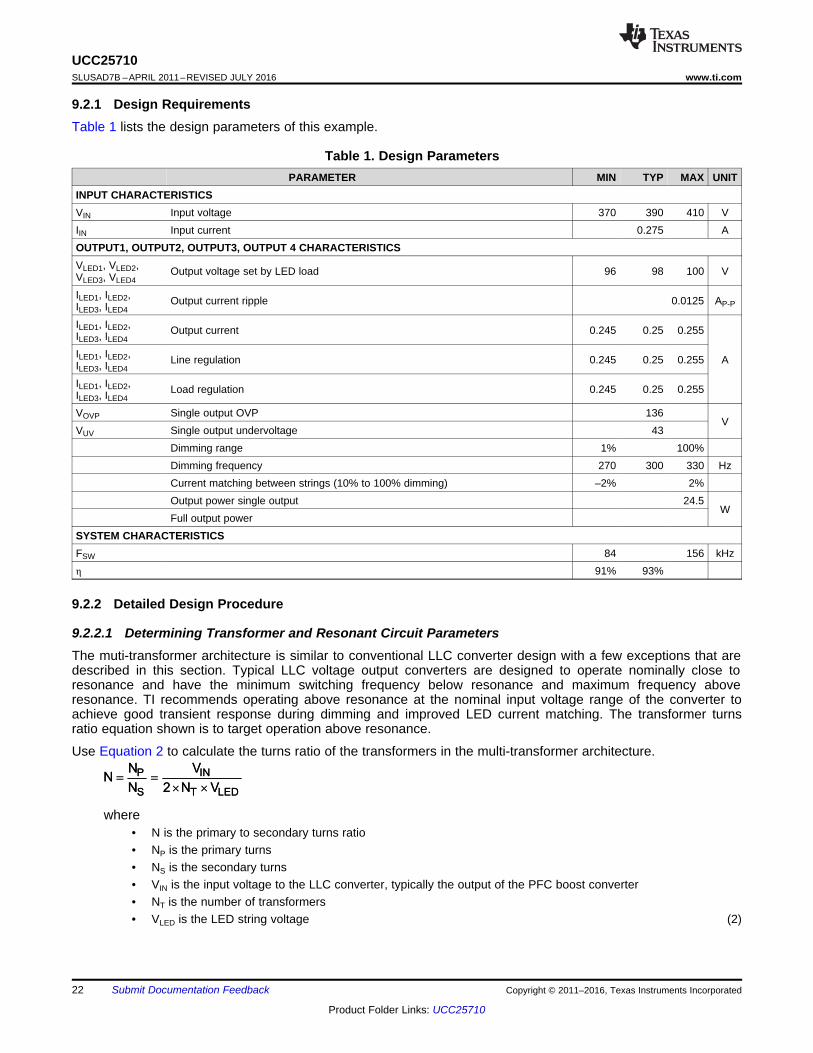
9.2.1 Design RequirementsTable 1 lists the design parameters of this example.
Table 1. Design ParametersPARAMETER MIN TYP MAX UNIT
INPUT CHARACTERISTICSVIN Input voltage 370 390 410 VIIN Input current 0.275 AOUTPUT1, OUTPUT2, OUTPUT3, OUTPUT 4 CHARACTERISTICSVLED1, VLED2,VLED3, VLED4
Output voltage set by LED load 96 98 100 V
ILED1, ILED2,ILED3, ILED4
Output current ripple 0.0125 AP-P
ILED1, ILED2,ILED3, ILED4
Output current 0.245 0.25 0.255
AILED1, ILED2,ILED3, ILED4
Line regulation 0.245 0.25 0.255
ILED1, ILED2,ILED3, ILED4
Load regulation 0.245 0.25 0.255
VOVP Single output OVP 136V
VUV Single output undervoltage 43Dimming range 1% 100%Dimming frequency 270 300 330 HzCurrent matching between strings (10% to 100% dimming) –2% 2%Output power single output 24.5
WFull output power
SYSTEM CHARACTERISTICSFSW 84 156 kHzη 91% 93%
9.2.2 Detailed Design Procedure
9.2.2.1 Determining Transformer and Resonant Circuit ParametersThe muti-transformer architecture is similar to conventional LLC converter design with a few exceptions that aredescribed in this section. Typical LLC voltage output converters are designed to operate nominally close toresonance and have the minimum switching frequency below resonance and maximum frequency aboveresonance. TI recommends operating above resonance at the nominal input voltage range of the converter toachieve good transient response during dimming and improved LED current matching. The transformer turnsratio equation shown is to target operation above resonance.
Use Equation 2 to calculate the turns ratio of the transformers in the multi-transformer architecture.
where• N is the primary to secondary turns ratio• NP is the primary turns• NS is the secondary turns• VIN is the input voltage to the LLC converter, typically the output of the PFC boost converter• NT is the number of transformers• VLED is the LED string voltage (2)
CREFCS
LEDTotal
VR
I=
+–
+–
+–
T1
T2
TN
NP NS
Lr
½ Cr
RL=VLED
ILED
Lm +–
Primary turns (NP), leakage
inductance (Lr), and magnetizing
inductance (Lm) are combined as
a series equivalent:
Lr’=Lr x NT
NP’=NP x NT
Lm’=Lm x NT
NT is the number of transformers
Secondary is combined as
parallel equivalent:
RL’=RL/NT
Ns is unchanged
Multi-Transformer Single Transformer Equivalent
T1
NP’ NS
Lr’
Lm’
RL’=RL
NT
½ Cr
½ Cr
½ Cr
UDG-11102
SW
0.5500nsIN
F
m
MPk T
V
L4 I N
æ ö´ -ç ÷ç ÷
è ø
´=
´
OSS INMPk
2 C VI
400ns
´´
=
23
UCC25710www.ti.com SLUSAD7B –APRIL 2011–REVISED JULY 2016
Product Folder Links: UCC25710
Submit Documentation FeedbackCopyright © 2011–2016, Texas Instruments Incorporated
Another important consideration for the multi-transformer LED driver is to set the total magnetizing inductance ofthe transformers as high as possible to minimize the primary magnetizing current and it’s effect on LED currentmatching. TI recommends targeting the total magnetizing inductance of the transformers to a value just lowenough to achieve ZVS operation during nominal frequency operation. Equation 3 and Equation 4 determine themagnetizing inductance target. Reduce the calculated LM to accommodate LM and COSS tolerances.
(3)
where• IMPk is the peak magnetizing current• COSS is the MOSFET equivalent time related drain to source capacitance• VIN is the nominal input voltage to the half bridge, normally the PFC output voltage• FSW is the switching frequency at the regulation operating point• LM is the magnetizing inductance of each transformer• NT is the number of transformers with the primaries in series (4)
To use standard LLC converter design process and available tools such as SLUC253 design calculator availableon the TI website, the multiple transformers and reflected loads can be combined into one equivalent transformerand load as shown in Figure 25. Once Lr and Lm are determined based on a single transformer circuit, simplydivide by the number of transformers for each transformer specification target.
Figure 25. Multiple Transformers Combined With Reflected Loads
9.2.2.2 CS (Output Current Sense)The CS pin is connected to the output current-sense resistor and is the feedback signal for the current amplifier.The regulation range is limited by the 0.5-V to 2.8-V internal current amplifier reference clamp. The LED currentsense resistor value is determined by Equation 5.
where
MAXSW
0.0664R
49.2pF F (Delta)=
´
SSSS
ICOMP _REG
2.5 A TC
V 0.9 V
m ´=
-
24
UCC25710SLUSAD7B –APRIL 2011–REVISED JULY 2016 www.ti.com
Product Folder Links: UCC25710
Submit Documentation Feedback Copyright © 2011–2016, Texas Instruments Incorporated
• VCREF is voltage on CREF pin determined by divider from VREF ILEDTotal.• ILEDTOTAL is the total LED string current during the DIM on time. (5)
9.2.2.3 ICOMP (Current Amplifier Compensation)Connect a capacitor or series resistor capacitor combination to ground to compensate the 510-µS GM currentamplifier control loop. The current amplifier is designed to maintain the steady-state operating voltage point of thecurrent amplifier during dimming operation. This is accomplished by switching on and off the GM current amplifierto the ICOMP pin with the same control signal that controls the LEDSW output. The GM amplifier is disconnectedfrom the ICOMP pin during the DIM OFF-time, and connected during the DIM ON-time. This feature iscompromised if there is a leakage path on the ICOMP pin, such as resistance to ground. The re-connection ofthe ICOMP pin to the current amplifier output is delayed by about 2.4 µs to allow time for the external LED switchto be turned on prior to allowing the ICOMP pin voltage to be driven.
The optimum ICOMP capacitor value is determined based on desired LED current and primary current responseduring dimming. Because the LLC converter has a highly nonlinear transfer function, a gain phase analyzer isrecommended to optimize the component values on ICOMP. The recommended bandwidth target is from 800 Hzto 5 kHz. The trade-off of too low bandwidth is increased line frequency ripple on the LED string current. Thetrade-off of high bandwidth is voltage variation on ICOMP during the DSR rise time which can result in primarycurrent peaking during the start of the DIM period, this may result in audible noise if excessive. Either anintegrator (capacitor to ground) or type II compensation (capacitor in parallel with resistor and series capacitor) isrecommended.
9.2.2.4 SS (Soft Start)Connect a capacitor to ground to program the desired soft-start time. When VCC exceeds the VCCON thresholdand BLON is high, a 2.5-µA current source charges the soft-start capacitor after a 10-ms delay. The voltage onSS dominates the VCO control voltage when lower than VICOMP or VDSR. The device is in a soft-start conditionuntil VSS reaches the 4.2-V soft start over threshold. During the soft-start cycle DIM is disabled and the UVprotection is disabled. The soft-start cycle is initiated by UVLO, BLON, OV fault clear, or UV fault clear after thesoft-start cycle.
where• TSS is the target SS time.• VICOMP_REG is the ICOMP voltage at the regulation point, which can be derived based on LLC switching
frequency. (6)
9.2.2.5 FMAX (Maximum VCO Frequency)Terminate FMAX to ground with a resistor to program the frequency delta from desired maximum to minimumoperating frequency range. The recommended resistor value range is 4.22 kΩ to 53.6 kΩ. VICOMP which is theVCO control signal determines the voltage on FMAX; the programming resistor determines the voltage to currentconversion ratio that programs the oscillator frequency at a given VICOMP voltage level. The device is designed toaccommodate a maximum frequency of 350 kHz and a minimum frequency delta of 25 kHz. To providecontrolled rise and fall time of the primary current during dimming, a maximum frequency of 2 to 3 times thenominal switching frequency is recommended as an initial value. The resistor value can be determined byEquation 7.
where• FSW(Delta) = FSW(max)-FSW(min) (7)
9.2.2.6 FMIN (Minimum VCO Frequency)Terminate FMIN to ground with a resistor to program the desired minimum operating frequency. Therecommended resistor range is 9.53 kΩ to 102 kΩ. The device is designed to accommodate a minimumfrequency of 30 KHz. The resistor value can be determined by Equation 8.

CCGD
SW
VL
2 F 87mA=
´ ´
CCGD
SW
VL
2 F 87mA=
´ ´
( )ICOMP
MIN MAXSW
4 V V0.15
R R 45.2VF
49.2pF
-+
´=
MINSW(min)
0.15R
49.2pF F=
´
25
UCC25710www.ti.com SLUSAD7B –APRIL 2011–REVISED JULY 2016
Product Folder Links: UCC25710
Submit Documentation FeedbackCopyright © 2011–2016, Texas Instruments Incorporated
(8)
Use Equation 9 to determine FSW for given VICOMP, RFMAX, and RFMIN values.
where from Equation 7 to Equation 9• FSW is in Hz, R is in Ω• VICOMP is in V (9)
9.2.2.7 GD1 and GD2 (Gate Drive 1 and 2)Connect the primary of the gate-drive transformer to GD1 and GD2 through a small series resistance. The high-side driver resistance is 12 Ω and low-side driver resistance is 4 Ω typical. The drivers are limited to 25-mA RMSmaximum current, so there is a magnetizing current limitation of the gate-drive transformer shown in theEquation 10. If the magnetizing current exceeds 25 mA with the specified gate-drive transformer and nominaloperating frequency, a simple NPN-PNP buffer on GD1 and GD2 may be required. The minimum gate drivetransformer inductance can be determined from Equation 10.
where• LGD is the gate drive transformer LPRI
• FSW is the nominal switching frequency• VCC is the VCC supply voltage (10)
9.2.2.8 LEDSW (LED Switch Drive)The LEDSW is the output to control the LED switch MOSFET in series with the LED string returns. The LEDSWis controlled by the DIM input during normal operation to provide LED string current pulse widths thatcorresponds to the DIM signal. During soft start, the LEDSW signal is high regardless of the DIM signal to allowthe output capacitors to charge. The LEDSW is low during an OV, UV or CL fault to provide additional protectionto the LED’s. This output is 0 V to VCC but has limited drive current ability, a simple NPN or PNP buffer isrequired to drive the LED switch MOSFET. The LEDSW high resistance is 4 kΩ and low side is 2 kΩ, so avoidany DC load on this pin.
The turnon and turnoff delay of the LED switch MOSFET relative to DIM rising and falling edge must be wellmatched to achieve excellent LED current linearity especially at low DIM duty-cycles. As an example, consider a1% dimming duty-cycle at dimming PWM frequency of 300 Hz where a delay mismatch of 667 ns represents a2% linearity error. A gate-drive resistor and parallel resistor diode combination to drive the LED switch MOSFETcan be used to match edge delays. Refer to Figure 26 for a recommended LED switch MOSFET drive circuit.
( )DTY DIMV 1 D 2.5 V 0.1Vé ù= - ´ +ë û
DTYDTY(pp) DIM
15.65 AC
V F
m=
´
SLEWDSR
ICOMP _REG
44 A TC
V 0.9 V
m ´=
-
UDG-11091
LED Strings
Common Return1
6
VCC
LEDSW
26
UCC25710SLUSAD7B –APRIL 2011–REVISED JULY 2016 www.ti.com
Product Folder Links: UCC25710
Submit Documentation Feedback Copyright © 2011–2016, Texas Instruments Incorporated
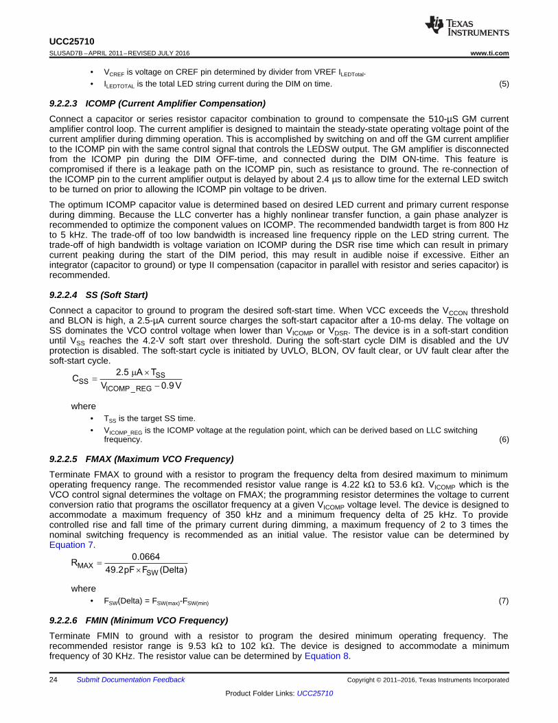
Figure 26. Recommended LED Switch MOSFET Drive Circuit
9.2.2.9 DSR (Dimming Slew Rate)The DSR pin is used to control the rise and fall time of the VCO control voltage. The DSR capacitor value can bedetermined by Equation 11. The effective rise time of the LLC primary current is when VDSR is between the 0.9-V gate-drive enable voltage and the VICOMP operating point.
where• TSLEW is the desired LLC current rise and fall time• VICOMP_REG is the ICOMP voltage regulation point (11)
Because the DSR voltage starts at 0 V and the LLC gate-drive enable is typically 0.9 V, there is a delay from theDIM rising edge and LEDSW rising edge until the LLC gate drivers are enabled. An easy solution to eliminate amajority of the delay is to use a resistor in series with CDSR. Because DSR is clamped at a Vbe above VICOMP,the recommended resistance is 15 kΩ to 17 kΩ to provide a 640-mV to 720-mV initial voltage delta.
9.2.2.10 DTY (Dimming Duty-Cycle Average)The DTY pin generates a voltage inversely proportional to the DIM duty-cycle with a 100-mV offset. The voltagerange is 100 mV to 2.6 V corresponding to 100% dimming and 0% dimming. This voltage is compared to theDADJ rising ramp to determine the dimming duty-cycle compensation delay time.
The capacitor value is selected to provide low ripple voltage at the DIM frequency. A good guideline is to target100 V or less peak-to-peak ripple voltage. There is a trade-off of DTY capacitor value and response to DIM duty-cycle transients. For faster response time to significant changes in DIM duty-cycle select a lower valuecapacitance. Equation 12 can be used to select a DTY capacitor based on maximum ripple voltage and DIMfrequency.
where• FDIM is the dimming frequency• VDTY(pp) is the maximum peak to peak ripple voltage. (12)
Equation 13 can be used to determine the average of VDTY at any given DIM duty-cycle.
where DDIM is the DIM duty-cycle. (13)

( )
DMIN RISE DMIN
DIM DIM
DADJ
DMIN
DIM T DIM20 A
F FC
1 DIM 2.5 V 0.1V
æ ö´m ´ -ç ÷ç ÷
è ø=é ù- ´ +ë û
27
UCC25710www.ti.com SLUSAD7B –APRIL 2011–REVISED JULY 2016
Product Folder Links: UCC25710
Submit Documentation FeedbackCopyright © 2011–2016, Texas Instruments Incorporated
9.2.2.11 DADJ (Dimming Duty-Cycle Adjust)The DADJ pin is a 20-µA current source enabled at the DIM falling edge. The capacitor connected to this pindetermines the slope of VDADJ. LLC-OFF is the internal signal that controls the turnon and turnoff of the LLCpower stage. The rising edge of LLC-OFF corresponds to a falling edge at the DIM input. The falling edge of theLLC-OFF signal is delayed until the rising edge of the DADJ voltage crosses the voltage on DTY. See DimmingOperation discussion for more details.
An initial value DADJ capacitor can be determined by Equation 14. The dimming performance at lowest DIM ontime must be evaluated as described in the following paragraph.
where• DIMDMIN is the minimum dimming duty cycle• FDIM is the dimming frequency• TRISE is the effective DSR rise time (14)
To ensure consistent LED current regulation during DIM duty-cycle transients, it is important to confirm thatICOMP achieves the steady-state operating voltage at the lowest DIM duty-cycle. Because DSR is clamped aVBE (approximately 0.7 V) above ICOMP, this signal can be inspected to confirm a steady-state operating point isachieved after the programmed DSR rise time. Confirm that the DSR signal achieves a relatively flat voltageduring the lowest DIM duty-cycle condition. Figure 27 and Figure 28 below are scope plots of 1% DIM duty-cyclewhere DSR reaches the steady-state operating point, and 0.5% DIM where DSR is still rising and ICOMP is openloop. If DSR is still rising during the lowest DIM duty cycle, increase the DADJ capacitor value until DSRachieves a relatively flat response as shown in Figure 27, the 1% DIM duty-cycle scope plot below.
Figure 27. 1% DIM duty-cycle Figure 28. 0.5% DIM duty-cycle
9.2.2.12 OV (Output Overvoltage)The OV pin is connected to an output-voltage sense resistor divider with oring diodes to all of the LED outputs.The OV threshold is 2.6 V with 240-mV hysteresis. During an OV fault the GD1 and GD2 gate drivers aredisabled and the LEDSW goes low (off). When the OV fault clears, the soft-start cycle is initiated.

OV1PU
RR
5=
LED1
LED2
LED3
LED4
RUV1
RUV2CUV
UV
ROV1
ROV2COV
OV
RPU
IBIAS
UDG-11103
OV1OV2
OVLO D
R 2.6 VR
V 2.6 V V
´
=
- -
OUTOV1
OUT MIN MATCH
2 V 1.5R
I D I
´ ´
=
´ ´
28
UCC25710SLUSAD7B –APRIL 2011–REVISED JULY 2016 www.ti.com
Product Folder Links: UCC25710
Submit Documentation Feedback Copyright © 2011–2016, Texas Instruments Incorporated
A configuration is shown in Figure 29 below that allows for summing of multiple LED string outputs into commonUV and OV dividers. Consider the total resistance of the divider networks because the divider bias current isprovided by the highest voltage LED string. Equation 15 and Equation 16 can be used to determine total dividerresistance and each component values.
where• VOUT is LED string voltage• IOUT is LED DC output current• DMIN is minimum dimming duty-cycle• IMATCH is LED current matching target• OV and UV dividers are approximately equal resistance (15)
where• VOVLO is the OVP threshold• VD is the summing diode voltage drop (16)
Figure 29. Application of Overvoltage and Undervoltage
9.2.2.13 UV (Output Undervoltage)UV is connected to an output-voltage sample of the converter. The UV threshold is 2.4 V with 240-mV hysteresis.UV below 2.4 V is considered an undervoltage fault which disables the GD1 and GD2 gate drivers, LEDSWoutput goes low, the 10-ms soft-start clamp and soft-start cycle are initiated. The UV comparator is disabled untilSS voltage is 4.2 V to allow the output capacitors to charge to the normal operating voltage during start-up of theconverter.
See the OV and UV divider diagram above for a typical configuration that allows for summing of multiple LEDstring outputs into common UV and OV dividers. Consider the value of RPU to avoid a current path from thehighest voltage LED string to the lowest voltage LED string. Equation 17, Equation 18, and Equation 19 assumea 2× VOUT delta as the maximum UVLO voltage.
where• LED voltage total tolerance is ±5%
10 70
85
93
95
40
88
90
Effic
ien
cy
-%
98-W EFFICIENCY WITH PWM DIMMING
86
89
91
94
100
Dimming - %
Efficiency 390 V
Efficiency 370 V
Efficiency 410 V
87
92
25 55 85
CH3 = Current Sense = V@R13CH4 = Primary Transformer Current
CH2 = Switch Node = Q2d CH1 = Switch Node = Q2g
Gate Drive Transition After Switch Node Achieving ZVS
( )UV1 PU
UV2
UVLO D
R R 2.4 VR
V 2.4 V V
+ ´=
- -
UV1 OV1 PUR R R= -
29
UCC25710www.ti.com SLUSAD7B –APRIL 2011–REVISED JULY 2016
Product Folder Links: UCC25710
Submit Documentation FeedbackCopyright © 2011–2016, Texas Instruments Incorporated
• OV and UV dividers are approximately equal resistance (17)
(18)
where• VUVLO is the UVP threshold• VD is the summing diode voltage drop (19)
9.2.2.14 CL (Current Limit)The CL pin is typically connected to the rectified and filtered output of a primary current sense transformer. Thereare two levels of current limit protection: restart and latching. When CL exceeds 0.95 V the gate drivers aredisabled and LEDSW goes low, when the CL voltage reduces to 475 mV the soft-start cycle is initiated. If CLexceeds a 1.9-V threshold, the gate drivers are disabled and LEDSW goes low, this condition is latched untilVCC is recycled below the UVLO threshold.
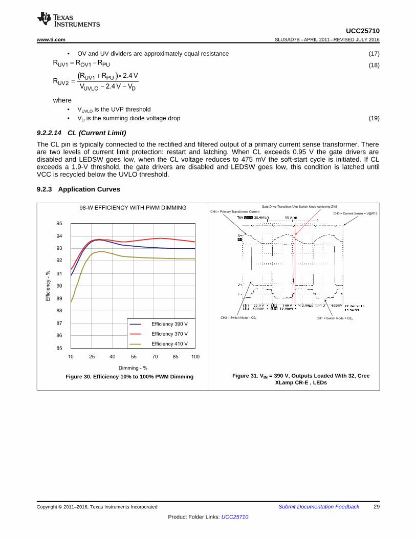
9.2.3 Application Curves
Figure 30. Efficiency 10% to 100% PWM Dimming Figure 31. VIN = 390 V, Outputs Loaded With 32, CreeXLamp CR-E , LEDs

CH1 = V@R13
CH4 = (LED4 +) Current
CH3 = (LED3 +) Current
CH1 = V@R13
CH4 = (LED2 +) Current
CH3 = (LED1 +) Current
CH1 = V@R13
CH4 = (LED4 +) Current
CH3 = (LED3 +) Current
CH1 = V@R13
CH4 = (LED2 +) Current
CH3 = (LED1 +) Current
CH1 = V@R13
CH4 = (LED2 +) Current
CH3 = (LED1 +) Current
CH1 = V@R13
CH4 = (LED4 +) Current
CH3 = (LED3 +) Current
30
UCC25710SLUSAD7B –APRIL 2011–REVISED JULY 2016 www.ti.com
Product Folder Links: UCC25710
Submit Documentation Feedback Copyright © 2011–2016, Texas Instruments Incorporated
Figure 32. Current LED1 (CH3) and LED2 (CH4) Figure 33. Current LED3 (CH3) and LED4 (CH4)
Figure 34. Current LED1 (CH3) and LED2 (CH4) Figure 35. Current LED3 (CH3) and LED4 (CH4)
Figure 36. Current LED1 (CH3) and LED2 (CH4) Figure 37. Current LED3 (CH3) and LED4 (CH4)
31
UCC25710www.ti.com SLUSAD7B –APRIL 2011–REVISED JULY 2016
Product Folder Links: UCC25710
Submit Documentation FeedbackCopyright © 2011–2016, Texas Instruments Incorporated
10 Power Supply RecommendationsThe UCC25710 is designed to operate from an external bias supply connected to the VCC input. It has anoperating voltage range between 11 V and 18 V with an absolute maximum input voltage rating of 18 V.
In most applications, the high voltage input range of the LLC controller is normally set at about 370 V to 410 Vwith 390-V nominal. This narrow range of DC input voltage is a constraint of the LLC topology. Setting themaximum and minimum switching frequencies limits the regulation range to these input voltages.
11 Layout
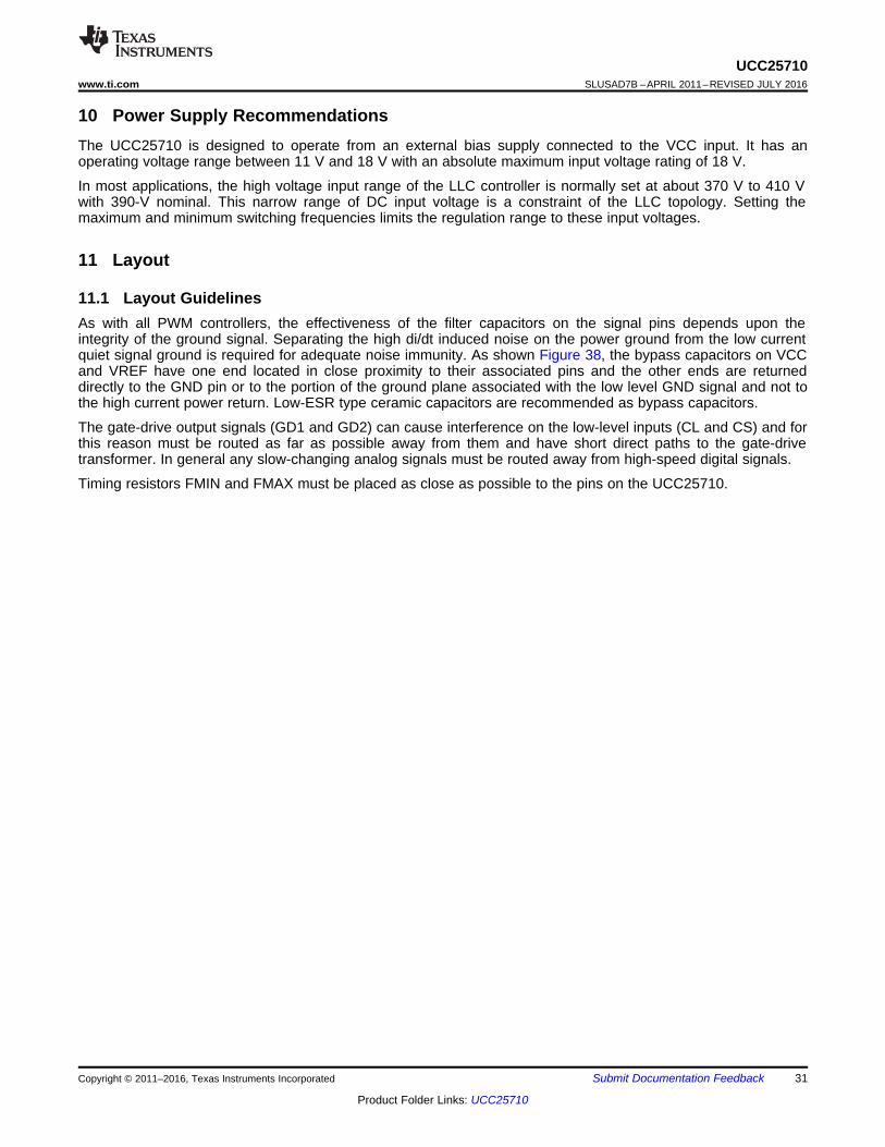
11.1 Layout GuidelinesAs with all PWM controllers, the effectiveness of the filter capacitors on the signal pins depends upon theintegrity of the ground signal. Separating the high di/dt induced noise on the power ground from the low currentquiet signal ground is required for adequate noise immunity. As shown Figure 38, the bypass capacitors on VCCand VREF have one end located in close proximity to their associated pins and the other ends are returneddirectly to the GND pin or to the portion of the ground plane associated with the low level GND signal and not tothe high current power return. Low-ESR type ceramic capacitors are recommended as bypass capacitors.
The gate-drive output signals (GD1 and GD2) can cause interference on the low-level inputs (CL and CS) and forthis reason must be routed as far as possible away from them and have short direct paths to the gate-drivetransformer. In general any slow-changing analog signals must be routed away from high-speed digital signals.
Timing resistors FMIN and FMAX must be placed as close as possible to the pins on the UCC25710.
1
11
20
10
GND
GND
VCC
VREF
CL
CS
32
UCC25710SLUSAD7B –APRIL 2011–REVISED JULY 2016 www.ti.com
Product Folder Links: UCC25710
Submit Documentation Feedback Copyright © 2011–2016, Texas Instruments Incorporated
11.2 Layout Example
Figure 38. Layout Example for UCC25710

33
UCC25710www.ti.com SLUSAD7B –APRIL 2011–REVISED JULY 2016
Product Folder Links: UCC25710
Submit Documentation FeedbackCopyright © 2011–2016, Texas Instruments Incorporated
12 Device and Documentation Support
12.1 Receiving Notification of Documentation UpdatesTo receive notification of documentation updates, navigate to the device product folder on ti.com. In the upperright corner, click on Alert me to register and receive a weekly digest of any product information that haschanged. For change details, review the revision history included in any revised document.
12.2 Community ResourceThe following links connect to TI community resources. Linked contents are provided "AS IS" by the respectivecontributors. They do not constitute TI specifications and do not necessarily reflect TI's views; see TI's Terms ofUse.
TI E2E™ Online Community TI's Engineer-to-Engineer (E2E) Community. Created to foster collaborationamong engineers. At e2e.ti.com, you can ask questions, share knowledge, explore ideas and helpsolve problems with fellow engineers.
Design Support TI's Design Support Quickly find helpful E2E forums along with design support tools andcontact information for technical support.
12.3 TrademarksE2E is a trademark of Texas Instruments.All other trademarks are the property of their respective owners.
12.4 Electrostatic Discharge CautionThese devices have limited built-in ESD protection. The leads should be shorted together or the device placed in conductive foamduring storage or handling to prevent electrostatic damage to the MOS gates.
12.5 GlossarySLYZ022 — TI Glossary.
This glossary lists and explains terms, acronyms, and definitions.
13 Mechanical, Packaging, and Orderable InformationThe following pages include mechanical, packaging, and orderable information. This information is the mostcurrent data available for the designated devices. This data is subject to change without notice and revision ofthis document. For browser-based versions of this data sheet, refer to the left-hand navigation.
PACKAGE OPTION ADDENDUM
www.ti.com 15-Feb-2016
Addendum-Page 1
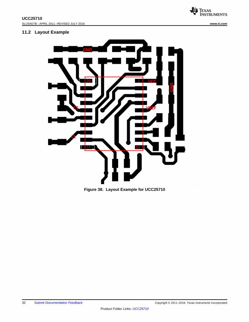
PACKAGING INFORMATION
Orderable Device Status(1)
Package Type PackageDrawing
Pins PackageQty
Eco Plan(2)
Lead/Ball Finish(6)
MSL Peak Temp(3)
Op Temp (°C) Device Marking(4/5)
Samples
UCC25710DW ACTIVE SOIC DW 20 25 Green (RoHS& no Sb/Br)
CU NIPDAU Level-1-260C-UNLIM -40 to 125 UCC25710
UCC25710DWR ACTIVE SOIC DW 20 2000 Green (RoHS& no Sb/Br)
CU NIPDAU Level-1-260C-UNLIM -40 to 125 UCC25710
(1) The marketing status values are defined as follows:ACTIVE: Product device recommended for new designs.LIFEBUY: TI has announced that the device will be discontinued, and a lifetime-buy period is in effect.NRND: Not recommended for new designs. Device is in production to support existing customers, but TI does not recommend using this part in a new design.PREVIEW: Device has been announced but is not in production. Samples may or may not be available.OBSOLETE: TI has discontinued the production of the device.
(2) Eco Plan - The planned eco-friendly classification: Pb-Free (RoHS), Pb-Free (RoHS Exempt), or Green (RoHS & no Sb/Br) - please check http://www.ti.com/productcontent for the latest availabilityinformation and additional product content details.TBD: The Pb-Free/Green conversion plan has not been defined.Pb-Free (RoHS): TI's terms "Lead-Free" or "Pb-Free" mean semiconductor products that are compatible with the current RoHS requirements for all 6 substances, including the requirement thatlead not exceed 0.1% by weight in homogeneous materials. Where designed to be soldered at high temperatures, TI Pb-Free products are suitable for use in specified lead-free processes.Pb-Free (RoHS Exempt): This component has a RoHS exemption for either 1) lead-based flip-chip solder bumps used between the die and package, or 2) lead-based die adhesive used betweenthe die and leadframe. The component is otherwise considered Pb-Free (RoHS compatible) as defined above.Green (RoHS & no Sb/Br): TI defines "Green" to mean Pb-Free (RoHS compatible), and free of Bromine (Br) and Antimony (Sb) based flame retardants (Br or Sb do not exceed 0.1% by weightin homogeneous material)
(3) MSL, Peak Temp. - The Moisture Sensitivity Level rating according to the JEDEC industry standard classifications, and peak solder temperature.
(4) There may be additional marking, which relates to the logo, the lot trace code information, or the environmental category on the device.
(5) Multiple Device Markings will be inside parentheses. Only one Device Marking contained in parentheses and separated by a "~" will appear on a device. If a line is indented then it is a continuationof the previous line and the two combined represent the entire Device Marking for that device.
(6) Lead/Ball Finish - Orderable Devices may have multiple material finish options. Finish options are separated by a vertical ruled line. Lead/Ball Finish values may wrap to two lines if the finishvalue exceeds the maximum column width.
Important Information and Disclaimer:The information provided on this page represents TI's knowledge and belief as of the date that it is provided. TI bases its knowledge and belief on informationprovided by third parties, and makes no representation or warranty as to the accuracy of such information. Efforts are underway to better integrate information from third parties. TI has taken andcontinues to take reasonable steps to provide representative and accurate information but may not have conducted destructive testing or chemical analysis on incoming materials and chemicals.TI and TI suppliers consider certain information to be proprietary, and thus CAS numbers and other limited information may not be available for release.
PACKAGE OPTION ADDENDUM
www.ti.com 15-Feb-2016
Addendum-Page 2
In no event shall TI's liability arising out of such information exceed the total purchase price of the TI part(s) at issue in this document sold by TI to Customer on an annual basis.

TAPE AND REEL INFORMATION
*All dimensions are nominal
Device PackageType
PackageDrawing
Pins SPQ ReelDiameter
(mm)
ReelWidth
W1 (mm)
A0(mm)
B0(mm)
K0(mm)
P1(mm)
W(mm)
Pin1Quadrant
UCC25710DWR SOIC DW 20 2000 330.0 24.4 10.8 13.3 2.7 12.0 24.0 Q1
PACKAGE MATERIALS INFORMATION
www.ti.com 15-Feb-2016
Pack Materials-Page 1
*All dimensions are nominal
Device Package Type Package Drawing Pins SPQ Length (mm) Width (mm) Height (mm)
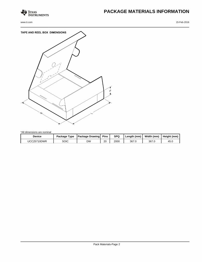
UCC25710DWR SOIC DW 20 2000 367.0 367.0 45.0
PACKAGE MATERIALS INFORMATION
www.ti.com 15-Feb-2016
Pack Materials-Page 2

www.ti.com
PACKAGE OUTLINE
C
TYP10.639.97
2.65 MAX
18X 1.27
20X 0.510.31
2X11.43
TYP0.330.10
0 - 80.30.1
0.25GAGE PLANE
1.270.40
A
NOTE 3
13.012.6
B 7.67.4
4220724/A 05/2016
SOIC - 2.65 mm max heightDW0020ASOIC
NOTES: 1. All linear dimensions are in millimeters. Dimensions in parenthesis are for reference only. Dimensioning and tolerancing per ASME Y14.5M. 2. This drawing is subject to change without notice. 3. This dimension does not include mold flash, protrusions, or gate burrs. Mold flash, protrusions, or gate burrs shall not exceed 0.15 mm per side. 4. This dimension does not include interlead flash. Interlead flash shall not exceed 0.43 mm per side.5. Reference JEDEC registration MS-013.
120
0.25 C A B
1110
PIN 1 IDAREA
NOTE 4
SEATING PLANE
0.1 C
SEE DETAIL A
DETAIL ATYPICAL
SCALE 1.200

www.ti.com
EXAMPLE BOARD LAYOUT
(9.3)
0.07 MAXALL AROUND
0.07 MINALL AROUND
20X (2)
20X (0.6)
18X (1.27)
(R )TYP
0.05
4220724/A 05/2016
SOIC - 2.65 mm max heightDW0020ASOIC
SYMM
SYMM
LAND PATTERN EXAMPLESCALE:6X
1
10 11
20
NOTES: (continued) 6. Publication IPC-7351 may have alternate designs. 7. Solder mask tolerances between and around signal pads can vary based on board fabrication site.
METALSOLDER MASKOPENING
NON SOLDER MASKDEFINED
SOLDER MASK DETAILS
SOLDER MASKOPENING
METAL UNDERSOLDER MASK
SOLDER MASKDEFINED
www.ti.com
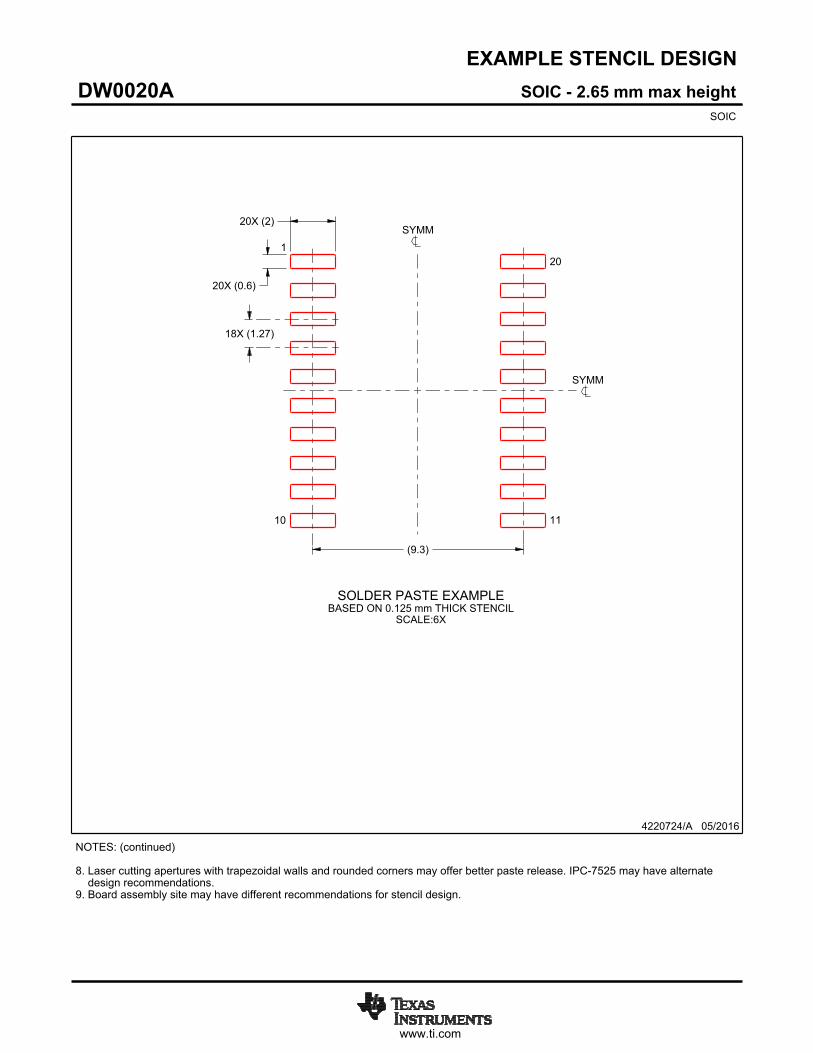
EXAMPLE STENCIL DESIGN
(9.3)
18X (1.27)
20X (0.6)
20X (2)
4220724/A 05/2016
SOIC - 2.65 mm max heightDW0020ASOIC
NOTES: (continued) 8. Laser cutting apertures with trapezoidal walls and rounded corners may offer better paste release. IPC-7525 may have alternate design recommendations. 9. Board assembly site may have different recommendations for stencil design.
SYMM
SYMM
1
10 11
20
SOLDER PASTE EXAMPLEBASED ON 0.125 mm THICK STENCIL
SCALE:6X
IMPORTANT NOTICE
Texas Instruments Incorporated and its subsidiaries (TI) reserve the right to make corrections, enhancements, improvements and otherchanges to its semiconductor products and services per JESD46, latest issue, and to discontinue any product or service per JESD48, latestissue. Buyers should obtain the latest relevant information before placing orders and should verify that such information is current andcomplete. All semiconductor products (also referred to herein as “components”) are sold subject to TI’s terms and conditions of salesupplied at the time of order acknowledgment.TI warrants performance of its components to the specifications applicable at the time of sale, in accordance with the warranty in TI’s termsand conditions of sale of semiconductor products. Testing and other quality control techniques are used to the extent TI deems necessaryto support this warranty. Except where mandated by applicable law, testing of all parameters of each component is not necessarilyperformed.TI assumes no liability for applications assistance or the design of Buyers’ products. Buyers are responsible for their products andapplications using TI components. To minimize the risks associated with Buyers’ products and applications, Buyers should provideadequate design and operating safeguards.TI does not warrant or represent that any license, either express or implied, is granted under any patent right, copyright, mask work right, orother intellectual property right relating to any combination, machine, or process in which TI components or services are used. Informationpublished by TI regarding third-party products or services does not constitute a license to use such products or services or a warranty orendorsement thereof. Use of such information may require a license from a third party under the patents or other intellectual property of thethird party, or a license from TI under the patents or other intellectual property of TI.Reproduction of significant portions of TI information in TI data books or data sheets is permissible only if reproduction is without alterationand is accompanied by all associated warranties, conditions, limitations, and notices. TI is not responsible or liable for such altereddocumentation. Information of third parties may be subject to additional restrictions.Resale of TI components or services with statements different from or beyond the parameters stated by TI for that component or servicevoids all express and any implied warranties for the associated TI component or service and is an unfair and deceptive business practice.TI is not responsible or liable for any such statements.Buyer acknowledges and agrees that it is solely responsible for compliance with all legal, regulatory and safety-related requirementsconcerning its products, and any use of TI components in its applications, notwithstanding any applications-related information or supportthat may be provided by TI. Buyer represents and agrees that it has all the necessary expertise to create and implement safeguards whichanticipate dangerous consequences of failures, monitor failures and their consequences, lessen the likelihood of failures that might causeharm and take appropriate remedial actions. Buyer will fully indemnify TI and its representatives against any damages arising out of the useof any TI components in safety-critical applications.In some cases, TI components may be promoted specifically to facilitate safety-related applications. With such components, TI’s goal is tohelp enable customers to design and create their own end-product solutions that meet applicable functional safety standards andrequirements. Nonetheless, such components are subject to these terms.No TI components are authorized for use in FDA Class III (or similar life-critical medical equipment) unless authorized officers of the partieshave executed a special agreement specifically governing such use.Only those TI components which TI has specifically designated as military grade or “enhanced plastic” are designed and intended for use inmilitary/aerospace applications or environments. Buyer acknowledges and agrees that any military or aerospace use of TI componentswhich have not been so designated is solely at the Buyer's risk, and that Buyer is solely responsible for compliance with all legal andregulatory requirements in connection with such use.TI has specifically designated certain components as meeting ISO/TS16949 requirements, mainly for automotive use. In any case of use ofnon-designated products, TI will not be responsible for any failure to meet ISO/TS16949.
Products ApplicationsAudio www.ti.com/audio Automotive and Transportation www.ti.com/automotiveAmplifiers amplifier.ti.com Communications and Telecom www.ti.com/communicationsData Converters dataconverter.ti.com Computers and Peripherals www.ti.com/computersDLP® Products www.dlp.com Consumer Electronics www.ti.com/consumer-appsDSP dsp.ti.com Energy and Lighting www.ti.com/energyClocks and Timers www.ti.com/clocks Industrial www.ti.com/industrialInterface interface.ti.com Medical www.ti.com/medicalLogic logic.ti.com Security www.ti.com/securityPower Mgmt power.ti.com Space, Avionics and Defense www.ti.com/space-avionics-defenseMicrocontrollers microcontroller.ti.com Video and Imaging www.ti.com/videoRFID www.ti-rfid.comOMAP Applications Processors www.ti.com/omap TI E2E Community e2e.ti.comWireless Connectivity www.ti.com/wirelessconnectivity
Mailing Address: Texas Instruments, Post Office Box 655303, Dallas, Texas 75265Copyright © 2016, Texas Instruments Incorporated