Embed Size (px)
Citation preview

東京大学 大学院新領域創成科学研究科
基盤科学研究系
先端エネルギー工学専攻
平成 22 年度
修士論文
Light-Weight Flexible Rectenna for
Wireless Power Transmission to Flying Objects
- 飛行体への無線電力伝送における軽量フレキシブルレクテナ -
2011 年 2 月提出
指導教員 小紫 公也 教授
96069 澤原 弘憲

Preface
This paper reports development of the light-weight flexible patch rectenna for the receiving
system. I designed and fabricated antennas, RF-DC conversion circuits, and rectennas, and measured
their power conversion efficiencies. As a result the antennas were developed with the average
polarized wave efficiency of 70% and the return loss efficiency of 99%. The RF-DC conversion
circuits were also developed with the conversion efficiency of maximum 58% at 65mW and 100
load resistance. Until this development, there were no high efficiency and light-weight flexible
rectenna. Therefore, the rectennas are very useful for Micro Aerial Vehicles and so on. Moreover, I
produced a rectenna array consisted of ten rectenna elements in parallel, and succeeded to operate
the electric motor for MAV model and demonstrate the MAV.
I would like to express my sincere appreciation to Professor Kimiya Komurasaki, Department
of Advanced Energy, University of Tokyo, for many valuable discussions, suggestions, supports and
encouragements. I’m grateful to express my thanks to Professor Yoshihiro Arakawa, Department of
Aeronautics and Astronautics, University of Tokyo, for his advice and discussion. Thanks also to Mr.
Oda, Ms. Ishiba, Mr. Ishida and Mr. Miyashiro who are Microwave Power Transmission Research
Group for the helping in the experiments. I would like to thank Associate Professor Koji Tanaka
(Institute of Space and Astronautical Science: ISAS, Japan Aerospace Exploration Agency: JAXA)
for his advice about the microwave power transmission and the experiment. I’m obliged to all the
member of Komurasaki lab and Arakawa lab, especially Messrs. Satoshi Nomura, Mr. Koizumi and
Mr. Mizuno for helping my research. Without any of these supports, this thesis would not have been
completed. Thank you so much.
Finally, I would like to my special appreciation to my parents for their financial and mental
support throughout my education.
February, 2011
Hironori Sawahara

Contents Ⅰ
Contents
List of figures Ⅳ
List of tables Ⅶ
Chapter 1 Introduction 1
1.1 Wireless Power Transmission 1
1.2 Microwave Wireless Power Transmission 3
1.3 MWPT to Micro Aerial Vehicle and Purpose of the thesis 5
Chapter 2 Basic Theory 7
2.1 Wave Propagation and Polarization 7
2.1.1 Linear polarized wave 7
2.1.2 Circular polarized wave 9
2.1.3 Polarization Choice for MAV 10
2.2 Transmission Line Theory 11
2.2.1 Wave Propagation on a Transmission Line 11
2.2.2 The Lossless Line 13
2.2.3 The Terminated Lossless Transmission Line 14
Chapter 3 Theories of Rectenna elements 15
3.1 Theory of Rectenna Design 15

Contents Ⅱ
3.2 Theory of Antenna Design 17
3.2.1 Size Designing of MSA 17
3.2.2 Impedance Matching Method between MSA element and Feeding System 17
3.2.3 Interior Electromagnetic Field of Rectangular MSA 19
3.2.4 Methods for Polarity-free Antenna 23
3.3 Theory of Rectifier Circuit Design 25
3.3.1 Rectifier Circuit Model in Lumped Parameter System 26
3.3.2 Matching of Input Impedance 28
3.3.3 Design of Stub 29
3.3.4 Output load-line Characteristics 30
3.3.5 Rectifier Circuit Model in Distributed Parameter System 32
Chapter 4 Experimental Apparatus 33
4.1 Power Transmission System 33
4.1.1 Oscillator 35
4.1.2 Power divider 36
4.1.3 6-bit digital phase shifter 37
4.1.4 Driver amplifier 38
4.1.5 Power amplifier 39
4.1.6 Booster amplifier 40
4.1.7 Horn antenna 41
4.1.8 Circularizer 42
4.2 Power Receiving System / Measurement Apparatus 43
4.2.1 Light-Weight Flexible Patch Antenna / Rectenna 44
4.2.2 Power Sensor and Power Meter 46
4.2.3 Adjustable Resistor 47
4.2.4 Digital Multi Meter 48
4.2.5 Signal Generator 48
4.2.6 Network Analyzer 49
4.3 Experimental Setup and Demonstration 50
4.3.1 Mounting structure 50
4.3.2 Electrical Motor for MAV Model 51
4.3.3 MAV Model and Demonstration 52

Contents Ⅲ
Chapter 5 Measurement Results and Discussions 54
5.1 Antenna Measurement 54
5.1.1 Dielectric Constant 54
5.1.2 Dependence of Yaw-Angle 56
5.1.3 Characteristic of Antenna (Return Loss) 57
5.2 RF-DC Conversion Circuit Measurement 59
5.2.1 Capacitance of Chip Condenser: C0 61
5.2.2 Length of Diode and Ground: lg 62
5.2.3 Pieces Number of the Low Pass Filter 63
5.2.4 Input Line Width: W 64
5.2.5 Diode Variations: D 65
5.2.6 Redesign of Rectifier Circuit 66
5.2.7 Bending Properties 67
5.2.8 Dependence of Input Power 68
5.3 Rectenna Array Measurement 69
5.3.1 Optimization of Array Pitch 69
5.3.2 Two Antenna Elements for One Rectifier Circuit 70
5.4 MAV Model Demonstration 72
5.4.1 Parallel Connection of Rectenna 72
5.4.2 Total Efficiency in Receiving System 73
5.4.3 MAV Model Demonstration 74
Chapter 6 Conclusions 75
6.1 Conclusions 75
6.2 Future Perspectives and Issues 76
References 77
Accomplishments 79

List of figures Ⅳ
List of figures
Figure 1.1 Classification of Wireless Power Transmission 1
Figure 1.2 Experiment of MWPT to a helicopter 4
Figure 1.3 Schematic of the MAV system 6
Figure 2.1 Schematic of Planar wave (TEM) Propagation 8
Figure 2.2 Schematic of Rotating Polarization Plane 9
Figure 2.3 Voltage and current definitions and equivalent circuit 12
Figure 2.4 A transmission line terminated in a load impedance ZL 14
Figure 3.1a Schematic of Rectenna 16
Figure 3.1b RF-DC Conversion Efficiency of Rectenna 16
Figure 3.2 Feeding Methods of MSA Element 18
Figure 3.3 Rectanglar MSA and its Coordinate System 19
Figure 3.4 Schematic of Electromagnetic Distribution of TM100 wave 22
Figure 3.5 Pattern of Unit of Multiple Dipole Antenna 23
Figure 3.6 Pattern of Patch Antenna for Circular Polarized Wave 24
Figure 3.7 Simple Schematic of Rectifier Circuit with Input and Output Filters 25
Figure 3.8 Schematic of Rectifier Circuit with Lumped-element Input and Output Filters 26
Figure 3.9 Schematic of Rectifier Circuit with a Transmission Line as Output Filter 26
Figure 3.10 Rectifier Circuit Pattern 27
Figure 3.11 Schematic of Rectifier Circuit for Experiment 27
Figure 3.12 Structure of Micro-Strip Line 28
Figure 3.13 Pattern and Equivalent Circuit of Micro-Strip Stub 29
Figure 3.14 Relationship between DC equivalent circuit and load-line 30
Figure 3.15 V-I Characteristic of Diode 31
Figure 3.16 Equivalent Circuit of Diode 32
Figure 3.17 Detailed Schematic of Rectifier Circuit for Experiment 32
Figure 4.1 Schematic of Transmitting Array antenna System 33

List of figures Ⅴ
Figure 4.2 Picture of Transmitting System (1: Power Amplifiers, 2: Driver Amplifiers,3: Phase
Shifters, 4: Booster Amplifier, 5: Oscillator, 6: 8 Power Divider, 7: Power Source) 34
Figure 4.3 Arrangement of five antenna elements of the array 34
Figure 4.4 Picture of Oscillator 35
Figure 4.5 Picture of Power Divider 36
Figure 4.6 Picture of Phase Shifter 37
Figure 4.7 Mechanism of phase shifting 37
Figure 4.8 Picture of Driver Amplifier 38
Figure 4.9 Picture of Power Amplifier 39
Figure 4.10 Picture of Booster Amplifier 40
Figure 4.11 Picture of Horn-Antenna 41
Figure 4.12 Picture of Circularizer 42
Figure 4.13 Schematic of Power Receiving System 43
Figure 4.14 Schematic of Characteristics Measurement of the Antenna and Rectifier Circuit 43
Figure 4.15 Picture of Light-Weight Flexible Patch Antenna and Rectenna 44
Figure 4.16 Schematic of Antenna 45
Figure 4.17 Picture of Powere Sensor (HP 437B) 46
Figure 4.18 Picture of Power Meter (HP 8481A) 46
Figure 4.19 Picture of Adjustable Resistor 47
Figure 4.20 Schematics of Circuit of Measurement of the Loded Output Voltage 47
Figure 4.21 Picture of Digital Multi Meter (kaise KU-1188) 48
Figure 4.22 Picture of Signal Generator (Hittite HMC-T2000) 48
Figure 4.23 Picture of Network Analyzer (HP 8722D) 49
Figure 4.24 Picture of Mounting Structure 50
Figure 4.25 Picture of Electrical Motor 51
Figure 4.26 Picture of MAV model 52
Figure 4.27 Picture of the Rectennas on the MAV model 53
Figure 4.28 Picture of the MAV Demonstration Setup 53
Figure 5.1 Picture of Liner-Polarized Wave Antenna 54
Figure 5.2 Picture of Circular-Polarized Wave Antenna and Antenna Size 55
Figure 5.3 Polarized Wave Properties 56
Figure 5.4 Return Loss of the Light-Weight Flexibel Antenna 57
Figure 5.5 Picture of Antenna and Bend Definition 58
Figure 5.6 Bending Properties of the Light-Weigh Flexible Antenna 58
Figure 5.7 Schematic of Rectifier Circuit Pattern Parameters 60
Figure 5.8 Load Characteristic related to Capacitance of Chip Condenser 61

List of figures Ⅵ
Figure 5.9 Load Characteristic related to D-G length 62
Figure 5.10 Schematic of Rectifier Circuit Pattern 63
Figure 5.11 Load Characteristic related to Number of LPFs 63
Figure 5.12 Load Characteristic related to Input Line Width 64
Figure 5.13 Load Characteristic related to Diode 65
Figure 5.14 Load Characteristic of New and Pre desig 66
Figure 5.15 Pictures of the Circuit and Bending definition 67
Figure 5.16 Bending Properties of the Light-Weigh Flexible RF-DC Conversion Circuit 67
Figure 5.17 Conversion Efficiency related to Input Power 68
Figure 5.18 Schematic of Rectenna Array Pitch 69
Figure 5.19 Picture of Rectenna with two antennas and one rectifier 70
Figure 5.20 Schematic of Parallel Connection of Rectenna 72
Figure 5.21 Schematic of Total Efficiency in Receiving System 73
Figure 5.22 DC Power related to Angle 74

List of tables Ⅶ
List of tables
Table 1.1 Classifications of EMR 3
Table 4.1 Specifications of Transmitting Array Antenna System 34
Table 4.2 Specifications of Oscllator 35
Table 4.3 Specification of the Driver Amplifier 38
Table 4.4 Specification of Booster Amplifier 40
Table 4.5 Specification of the Antenna 45
Table 4.6 Specification of the Motor 51
Table 4.7 Specification of MAV model 52
Table 5.1 Return Loss and Resonance Frequency of Antennas 55
Table 5.2 Specifications of Circular-Polarized Wave Antenna 55
Table 5.3 Bending Properties and Efficiency of the Light-Weight Flexilbe Antenna 58
Table 5.4 Parameters for Standard Rectifier Circuit Pattern 60
Table 5.5 Specifications of four Diodes 65
Table 5.6 Parameters of New Design Rectifier Circuit Pattern 66
Table 5.7 Measurement Result of each array pitch 69
Table 5.8 Output Voltage of each rectenna 70
Table 5.9 Comparison with some rectennas 71

1.1 Wireless Power Transmission 1
Chapter 1
Introduction This chapter shows the background and the purpose of this thesis.
1.1 Wireless Power Transmission
Power supply methods are generally wire transmission methods using power line from power
stations and codes from consents. However information-communication technology is become to be
wireless, for examples television, radio, mobile phone and wireless LAN. Therefore power supply
system changes from wire to wireless. Today, a lot of research and development about mobile
ubiquitous equipments and wireless power supply are conducted for short charging time, easier
charging, home appliance which can be anywhere, light battery capacity or resources and
environment preservation such as reduction of code and harness which are around room and car.[1], [2]
Wireless Power Transmission is divided into some parts for the transmission range as in Figure 1.1.
Figure 1.1 Classification of Wireless Power Transmission

1.1 Wireless Power Transmission 2
Power supplying in short range is generally used electromagnetic induction. Electromagnetic
induction is the production of voltage across a conductor moving through a magnetic field. This
electromagnetic induction method of wireless power transmission has small power loss but short
transmission range. The applications are, for example, passenger’s cards of trains and buses and
electric money cards.
Secondly, wireless power transmission in middle range is explained. Middle range means about
L/D = 1 length, which D is antenna’s size and L is transmission length. In the range, we are not able
to transmit power effectively using electromagnetic induction method. Instead of the electromagnetic
induction method, in the range, we can use strongly-coupled resonance method. The method is new
technique and Professor Marin Soljacic et al. at MIT[3]
reported in 2006. In the theory, used not
electromagnetic wave but electric or magnetic field, the power is transmitted from dielectric or
resonating valance bond to the receiver. Because of this advantage such as longer transmission range
and higher efficiency than the induction method, the strongly-coupled resonance method receives
much attention as a new technique of wireless power transmission.
Finally, there is electromagnetic beam radiation method as technology of wireless power
transmission to further range than wavelength. It is generally thought that electromagnetic radiation
cannot transmit power sufficiently because the radiation diffuses with the transmission length.
However a formation of electromagnetic beam makes the transmission length be extremely longer
with small loss. This technology have been mainly focused on the space field, so power transmission
to lunar probe using laser[4]
and large power transmission from solar power satellite to the ground[5]
have studied. Recently there has been interest in wireless power supply of robots and unmanned
aircrafts.

1.2 Microwave Wireless Power Transmission 3
1.2 Microwave Wireless Power Transmission
Electromagnetic radiation (EMR) is a form of energy exhibiting wave like behavior as it travels
through space.EMR has both electric and magnetic field components, which oscillate in phase
perpendicular to each other and perpendicular to the direction of energy propagation. EMR is applied
to lots of technologies such as information-communication technology. Table 1.1 shows
classifications of frequency of EMR and these applications.
Table 1.1 Classifications of EMR

1.2 Microwave Wireless Power Transmission 4
Microwaves are electromagnetic waves with wavelength ranging from as long as one meter to
as short as one millimeters, or equivalently, with frequencies between 0.3 GHz and 300 GHz. In all
cases, microwave includes the entire SHF band (3 to 30 GHz, or 10 to 1 cm) at minimum, with RF
engineering often putting the lower boundary at 1 GHz (30 cm), and the upper around 100 GHz (3
mm). Microwave technology is first developed as radar technology in 1940s. The radar uses the
characteristics of microwaves which travel in a straight line because of the short wavelength and
reflect off an object which has size above the wavelength. After that microwaves have had a wide
filed of application because of the advantage of straight traveling and the large transmission capacity
of information. Microwaves are applied to mobile phones and satellite communications as
transmission signals, microwave ovens using dielectric heat of microwaves, radio astronomy,
particle acceleration and medical devices. Then microwave technology has attracted much attention.
Microwave Wireless Power Transmission (MWPT) is first reported by W. C. Brown in 1960s[6],
[7]. Since he succeeded microwave power transmission to a helicopter (Figure 1.2), MWPT is applied
to large applications such as Solar Power System in space (SPS) and also small applications such as
micro robots which can move with small power because MWPT has long transmission range.
Figure 1.2 Experiment of MWPT to a helicopter

1.3 MWPT to Micro Aerial Vehicle and Purpose of the thesis 5
1.3 MWPT to Micro Aerial Vehicle and Purpose of the thesis
Conventional transportation systems, for example cars and aircrafts, are able to have long
ranning distances and high mobility with loading some fuels of high energy densities. However it is
difficult to replace such abilities to battery’s abilities. To run longer without power supply, the
systems need larger capacities of charge. Therefore batteries need more mineral resources, the
weight of the batteries is larger than that of passengers and loads and the total efficiency become to
be lower. To degrease the weigh and load of the batteries, the systems need to be supplied power
frequently at the supply station, so techniques of wireless power transmission are necessary. Micro
robots, which developed for surveillance and checking of devastated district, medical examination of
body and so on, are used. However the robots sometimes cannot move with their size, wire and
weight. Without batteries, their duration, size and range of moving are not be regulated. These days
ICs, sensors and LEDs have been developed at mW levels, so higher functions devices without
batteries are able to be designed and new applications are expected.
Micro Aerial Vehicle (MAV) is a power beaming system and an unmanned aircraft [8] - [15]
. With
this wireless power transmission system, a battery on a vehicle is charged by receiving a microwave
beam while the vehicle is circling above a phased array transmitter. Then, it can fly over the area
struck by disaster, for example, continuously without landing and take-off for recharging. Figure 1.3
shows the schematic of the system developed in our laboratory. It consists of three sub-systems; a
transmission system[8], [10], [11], [14], [15]
, a tracking system[8], [10], [11], [14], [15]
, and a receiving system[9],
[12], [13]. The MAV is tracked using the phase information of pilot signal. Software retro-directive
function has been realized through a PC control and a microwave beam is pointed to the MAV using
an active phased array. An electric motor for a propeller is driven by the power received on a
rectenna array. Rectenna has antenna and RC-DC conversion circuit which converts microwave
power to DC power.
Generally, conventional rectennas are made by etching copper foils based on solid dielectric
boards. However the geometry of a MAV is often curvature, therefore rectenna should be flexible to
utilize the geometry at a maximum. In addition the MAV should be light weight, so rectenna is also
necessary to be light weight. However, few studies have been reported on the light weight and
flexible rectennas, and very few other studies of the high efficiency, light weight and flexible patch
rectennas has appeared.
The purpose of this study has been to develop a light-weight flexible patch rectenna for the
MAV system and to demonstrate the MAV system especially the receiving system.

1.3 MWPT to Micro Aerial Vehicle and Purpose of the thesis 6
Figure 1.3 Schematic of the MAV system

2.1 Wave Propagation and Polarization 7
Chapter 2
Basic Theory This chapter is explained about microwave basic theory. Further details or information are
written in “Microwave Engineering[16]
”.
2.1 Wave Propagation and Polarization
There are two polarized waves; linear polarized wave and circular polarized wave. I explain the
polarization theories and the reasons why the polarity-free antennas are needed below.
2.1.1 Linear polarized wave
Electromagnetic wave, including microwave, has a polarization. When an electromagnetic wave
propagates through an uniform medium, the Maxwell equations are expressed with a charge density
=0 as:
0
0
H
E
EEH
HE
t
t
(2.1)
where is a dielectric constant and is a conductivity of the medium. Generally, an electromagnetic
wave varies at a constant frequency as sine curve, the electric field E and the magnetic field H are
expressed as:
tie
0EE (2.2)
tie
0HH (2.3)
where w is an angular frequency. Since they include phase terms, these E, E0, H, H0 are complex
variables and the absolute values of E0, H0 are the amplitude of the electric field and that of the
magnetic field. The real waves are expressed by their real parts.
Moreover, let the partial differentiation about time t jt and divide the electrical field

2.1 Wave Propagation and Polarization 8
and the magnetic field to x, y and z element, then the equation (2.1) is converted as:
zxy
yzx
x
yz
zxy
yzx
x
yz
Ejy
H
x
H
Ejx
H
z
H
Ejz
H
y
H
Hjy
E
x
E
Hjx
E
z
E
Hjz
E
y
E
(2.4)
When an electromagnetic wave propagates as a planar wave, there is no change of the electric
field and the magnetic field in the x-y plane at right angles to the propagating direction (z axis). Or
the solutions differentiating these fields with respect to x and y are 0. Under this condition, the z
axial component of the electromagnetic field varying temporally is expressed as:
0 zz HE (2.5)
Figure 2.1 shows the electromagnetic wave called “transverse electro magnetic (TEM) wave” or
“linear polarized wave;” the temporally homogeneous electromagnetic wave without the component
in the propagation direction of the electric field and the magnetic field. Additionally the plane
formed by the direction of the electric field and the wave propagating direction is called the
“polarization plane.”
Electric Field E x
Magnetic Field H y
x
y
z
Figure 2.1 Schematic of Planar wave (TEM) Propagation

2.1 Wave Propagation and Polarization 9
As a result, the equation (2.4) is figured as:
[x-direction polarization]
x
y
yx
Ejz
H
Hjz
E
(2.6)
[y-direction polarization]
yx
x
y
Ejz
H
Hjz
E
(2.7)
The x-direction polarization has only an x component of the electric field and a y component of
the magnetic field as Figure 2.1, and the y-direction polarization is the equivalent of the x-direction
one rotated by 90 degrees around the propagation direction. Furthermore, they can exist
independently of each other. With the linear polarized wave, we can obtain power only with the
antennas of the same polarization as the incident wave: the set of horizontal antennas and horizontal
wave, or of vertical antennas and vertical wave.
2.1.2 Circular polarized wave
Linear polarized waves are able to generate only artificially, and the polarization plane of
natural electromagnetic waves are temporally rotating. Figure 2.2 shows its schematic. It is called
“circular polarized wave.” We can generate circular polarized waves by combining the linear
polarized waves.
Electric Field E x
Magnetic Field H y
x
y
z
Figure 2.2 Schematic of Rotating Polarization Plane

2.1 Wave Propagation and Polarization 10
When there are two linear polarized waves, the electric field component of the x-direction
polarized wave is expressed as:
ztaEx cos (2.8)
where is a phase constant, and that of the y-direction polarized wave with the phase delaying by
is also expressed as:
ztbEy cos (2.9)
When two polarized waves with different phases exist, the circular polarized wave is generated with
combining them. (When there is no phase difference, or =0, the combined wave is just a linear
polarized wave at an angle with the x-axis.)
Under the special condition where =/2, a=b, Ex and Ey are represented as:
ztaztaE
ztaE
y
x
sin2cos
cos (2.10)
and then:
222 aEE yx (2.11)
From this, the combined electric field plane is rotating around any z position within its radius a. In
turn, this wave is propagating to the z direction at the phase velocity vp with rotating around the
z-axis at the angular rate . This wave called “circular polarized wave.” Under the general condition
where not both =/2 and a=b, the field locus is the ellipse and the wave called “elliptical polarized
wave.”
2.1.3 Polarization Choice for MAV
In this thesis, since the objective was the power transmission, not signal transmission, I needed
the high-efficient and simple system. The circular polarized wave can ignore the characteristic of the
polarization plane. However, it is unsuitable for the power transmission because of its lower
transmitting efficiency by reflections with transmitting and receiving than the linear one. The linear
one can achieve high efficiency and simple control system, then as with many researches, I adopted
it for the power transmitting system. Furthermore, since the MAV will move with random yaw angle
in spite of the fixed polarization plane by the linear polarized transmitting wave, we need to make
the receiving device polarity-free.

2.2 Transmission Line Theory 11
2.2 Transmission Line Theory
In many ways transmission line theory bridges the gap between field analysis and basic circuit
theory, and so is of significant importance in microwave analysis.
2.2.1 Wave Propagation on a Transmission Line
As shown in Figure 2.3a, a transmission line is often schematically represented as a two-wire
line, since transmission lines always have at least two conductors. The short piece of line of length
z of Figure 2.3a can be modeled as a lumped-element circuit, as shown in Figure 2.3b, where R, L,
G, C are per unit length quantities defined as follows:
R = series resistance per unit length, for both conductors, in /m.
L = series inductance per unit length, for both conductors, in H/m.
G = shunt conductance per unit length, in S/m.
C = shunt capacitance per unit length, in F/m.
From the circuit of Figure 2.3b, Kirchhoff’s voltage and current low can be applied to give
0),Δ(),(
Δ),(Δ),(
tzzv
t
tzizLtzziRtzv , (2.12)
0),Δ(),Δ(
Δ),(Δ),(
tzzi
t
tzzvzCtzzzvGtzi . (2.13)
Dividing (2.12) and (2.13) by Δz and taking the limit as Δz → 0 gives the following differential
equations:
t
tziLtzRi
z
tzv
),(),(
),(, (2.14)
t
tzvCtzGv
z
tzi
),(),(
),(. (2.15)
These equations are the time-domain form of the transmission line, or telegrapher, equations.
For the sinusoidal steady-state condition, with cosine-based phasors, (2.14) and (2.15) simplify
to
)()()(
zILjRdz
zdV , (2.16)
)()()(
zVCjGdz
zdI . (2.17)
The two equations of (2.16) and (2.17) can be solved simultaneously to give wave equations for
V(z) and I(z):

2.2 Transmission Line Theory 12
0)()( 2
2
2
zVdz
zVd , (2.18)
0)()( 2
2
2
zIdz
zId , (2.19)
where CjGLjRj )(( (2.20)
is the complex propagation constant, which is a function of frequency. Traveling wave solutions to
(2.18) and (2.19) can be found as
z
o
z
o eVeVzV )( , (2.21)
z
o
z
o eIeIzI )( . (2.22)
where the e-z
term represents wave propagation in the +z direction, and the ez
term represents wave
propagation in the –z direction.
Comparison with (2.21) and (2.22) shows that a characteristic impedance, Z0, can be defined as
CjG
LjRLjRZ
0 , (2.23)
Then (2.22) can be rewritten in the following form:
zozo e
Z
Ve
Z
VzI
00
)(
. (2.24)
Figure 2.3 Voltage and current definitions and equivalent circuit

2.2 Transmission Line Theory 13
2.2.2 The Lossless Line
The above solution was for a general transmission line, including loss effects, and it was seen
that the propagation constant and characteristic impedance were complex. In many practical cases,
however, the loss of the line is very small and so can be neglected, resulting in a simplification of the
above results. Setting R = G = 0 in (2.20) gives the propagation constant as
LCjj , (2.25)
or LC , (2.26)
0 , (2.27)
where is the propagation constant, is the phase constant and is the attenuation constant. As
expected for the lossless case, the attenuation constant is zero. The characteristic impedance of
(2.23) reduces to
C
LZ 0 , (2.28)
which is now a real number. The general solutions for voltage and current on a lossless transmission
line can then be written as
zj
o
zj
o eVeVzV )( , (2.29)
zjozjo e
Z
Ve
Z
VzI
00
)(
. (2.30)
The wavelength is
LC
22 , (2.31)
and the phase velocity is
LC
v p
1
. (2.32)

2.2 Transmission Line Theory 14
2.2.3 The Terminated Lossless Transmission Line
Figure 2.4 shows a lossless transmission line terminated in an arbitrary load impedance ZL.
Assume that an incident wave of the form Vo+ e
-jz is generated from a source at z <0. The total
voltage and total current on the line can be written as in (2.29) and (2.30), as a sum of incident and
reflected waves. The total voltage and current at the load are related by the load impedance, so at z =
0 we must have
00)0(
)0(Z
VV
VV
I
VZ
oo
oo
. (2.33)
The amplitude of the reflected voltage wave normalized to the amplitude of the incident voltage
wave is known as the voltage reflection coefficient, :
0
0
ZZ
ZZ
V
V
L
L
o
o
. (2.34)
When the load is mismatched, then, not all of the available power from the generator is
delivered to the load. This “loss” is called return loss (RL), and is defined (in dB) as
log20RL dB. (2.35)
At a distance l = -z from the load, the input impedance seen looking toward the load is
02
2
01
1
)(
)(Z
e
eZ
eeV
eeV
lI
lVZ
lj
lj
ljlj
o
ljlj
oin
, (2.36)
by using (2.34) for in (2.36):
ljZZ
ljZZZZ
L
Lin
tan
tan
0
00
. (2.37)
This is an important result giving the input impedance of a length of transmission line with an
arbitrary load impedance.
Figure 2.4 A transmission line terminated in a load impedance ZL

3.1 Theory of Rectenna Design 15
Chapter 3
Theories of Rectenna elements This chapter shows the theories of the rectenna elements including antenna elements and
rectifier circuit elements. Further details and information are written in “Antenna Theory and Design
Revised Edition[17]
”.
3.1 Theory of Rectenna Design
“Rectenna” is a device receiving the transmitted microwave power as radio frequency (RF) and
converting alternating current (AC) to direct current (DC) by rectifying. It is the coined term for
“RECTifier” and “antENNA”. Figure 3.1a shows its schematic. It normally consists of a receiving
antenna, an input filter, a rectifier and a output filter for smoothing power. Since the receivable
power with a rectenna is not enough large to operate systems, we use as a array of some rectennas
arranged and connected in series and in parallel each other.
One of the determining factors of the power conversion efficiency of a rectenna is the
characteristic of the important element of a rectifier, or a diode[18]
. Figure 3.1b shows the RF-DC
conversion efficiency characteristic of a rectenna. When the input power Pin decrease, the conversion
efficiency will become reduced. It is because the voltage between the both ends of a diode Vd will
become smaller than the diode forwarding voltage Vf, and then the rectifying feature of the diode
will not work (the Vf effect). Although the conversion efficiency increase as Pin becomes larger,
when Vd surpass the diode breakdown voltage VR, will also become reduced. It is because the
reverse current starts to flow (the VR effect). Moreover, will also become reduced because the high
order radio-frequency re-radiation generated with rectifying (the higher order harmonics effect).
Furthermore, the load resistance connected to the rectenna output has the optimal values; it is
the value in matching the output impedances of the rectenna with the load and also depends on Pin.,
Although there is no reflected wave with connecting the optimal load, there is reflected waves and
decreased without it. As a result, the diode maximum efficiency curve has a peak value depending on
the input power Pin and the load resistance RL.

3.1 Theory of Rectenna Design 16
Antenna Array (Right Face)
Rectifier Array (Rear Face)
Cupper (Ground)
Cupper (Antenna)Cupper (Rectifier)
Dielectric
Medium
Combine
Figure 3.1a Schematic of Rectenna
Input Power P in
L
R
R
V
4
2
Co
nv
ers
ion
Eff
icie
ncy
100%
Diode Max.
Efficiency
V R Effect
V f Effect
Higher order
Harmonics Effect
Figure 3.1b RF-DC Conversion Efficiency of Rectenna

3.2 Theory of Antenna Design 17
3.2 Theory of Antenna Design
There are many kinds of Antenna; horn antennas, monopole antenna, dipole antennas, slot
antennas, etc[17], [19], [20]
. In this thesis, we adopted the plane patch antennas because of the simplicity
of structure, the miniaturization in the size and the lightness.
The typical examples of the plane antennas are MSA (Micro Strip Antenna) elements. They
function as the microwave radiators composed of the planar circuit resonance elements with the
circular or quadrangular open boundary on the printed circuit boards (PCBs). Generally the substrate
for the MSA require low dielectric constant (r = 1.2~5.0) and low dielectric loss (tan=10-3
~10-4
),
such as the teflon-fiberglass substrate. In request for weight saving of wider band width (low Q
value), the paper-honeycomb substrate are used.
The size of the MSA elements is normally the half wavelength or less. The main mode is used
as a specimen excitation mode, and the MSA radiation pattern of the main mode shows the
unidirectionality with the maximum value in the front direction (z-axis) of the antenna pattern of
both the circular and quadrangular MSA. Thus, MSA enables to achieve the unidirectional pattern
without additional reflectors and to compose the thin and compact antenna simply.
3.2.1 Size Designing of MSA
The size of antennas depends on the target microwave wavelength. Generally the half
wavelength resonance method is used, and its resonance direction length is g/2. The g is the
wavelength of the microwave passing through a medium and is approximately expressed by:
r
g
0 (3.1)
where 0 is the free-space wavelength and r is the dielectric constant of the medium. In this thesis,
the size of square MSA for 5.8GHz was about 1.22cm on a side, 1.484cm2 with the glass-epoxy
substrate FR-4 (r=4.7). I explain the more details in 0.
3.2.2 Impedance Matching Method between MSA element and Feeding System
Figure 3.2 shows the typical feeding methods of the MSA. The input impedance Zin of the MSA
excited in the main mode depends on the predetermined feeding point 0[21]
. Zin at the resonance
point and around the near frequency domain vary from 0 (center) to several hundred ohms (open
boundary) by 0. Thus, with feeding at the edge (open boundary) of the MSA elements, the
resonance Zin exhibits a high impedance characteristic about 300~500. Consequently, we need for
it to match up with the feeding system about 50 of the characteristic impedance. In the
backside-coaxial feeding method, we can match up the impedances by offsetting the position 0 of
the feeding point F. Generally, the offset ratio is about 30%; (0/a)=0.3 in the circular MSA,

3.2 Theory of Antenna Design 18
(0/(a/2)=0.3) in the quadrangular MSA. In the coplanar feeding method, we can also match up the
impedance of the antenna with one of the main feeding line Fm by the g/4 impedance transformer Tf.
In the electromagnetic coupling feeding method, it is adopted to set the insert length l0 to the
specimen excitation slot of the feeding strip line at about g/4, and to control the values of the
specimen excitation slot width w, its slot length ls and the offset length 0. In this thesis, we adopted
the backside-coaxial feeding method and 0.3 of 0 because of the simplicity of its fabrication and the
connectivity with the rectifier circuits.
0
a
x
y
r
F
G
S
R
G
S
R
0
a
x
y
r
F
b
Tf
Fm
0
x
y
r
l s
l 0
w
b) Coplanar Feeding Method
a) Backside-Coaxial Feeding Method
c) ElectroMagnetic (EM) Coupling Feeding Method
R : Radiator element
S : dielectoric Substrate
G : Ground
F : Feeding point
Figure 3.2 Feeding Methods of MSA Element

3.2 Theory of Antenna Design 19
3.2.3 Interior Electromagnetic Field of Rectangular MSA
Figure 3.3 shows the analysis model of the inner electromagnetic field of a rectangular MSA.
When the substrate thickness t is enough smaller than the free-space wavelength 0 (k0t<<1; k0 is a
free-space wavenumber), TMmn0 wave is excited; it has an electric field element only to the direction
of t (z direction).
t
z
yx
a b
C
dl
*
F
R
P (R,q ,)
q
r
r
# 1
# 2
# 4
# 3
Ground
(F: Feeding point)Substratum
a) Coordinate System
b
a
x
M 1
M 2
M 3 M 4
b) Example of Magnetic Current
Figure 3.3 Rectanglar MSA and its Coordinate System

3.2 Theory of Antenna Design 20
The electromagnetic field of this TMmn0 wave is expressed by follow wave equation:
022 zt Ek (Interior region) (3.2)
0
n
E z (Open boundary) (3.3)
where n̂ is outward unit normal vector at the open boundary and ∇2t is 2222 yx .
When we separate variables of Ez element as Ez=X(x)Y(y) and of k element as k2=kx
2+ky
2 into x
and y directions, and assign it to the equation (3.2):
2
2
21xk
x
X
X
(3.4)
2
2
21yk
y
Y
Y
(3.5)
where kx=m/a of a wavenumber in x direction and ky=n/b in y direction. by using the separation of
variables, Ez element of TMmn0 wave is expressed by:
2cos
2cos0
ny
b
nmx
a
mEEz
(3.6)
22
222
b
n
a
mkkk yx
(3.7)
where E0 is an arbitrary number, k is the wavenumber in the dielectric, and m and n are
arbitrary integers. Additionally, we assign this Ez to the Maxwell equation and consider the TM wave
condition (Hz=0), then we can find the interior electromagnetic elements of the rectangular MSA as:
0
2cos
2cos
2sin
2cos
2cos
2cos
0
2
0
2
0
zyx
y
x
z
HEE
nx
b
nmx
a
m
t
V
a
m
k
jH
nx
b
nmx
a
m
t
V
b
n
k
jH
nx
b
nmx
a
m
t
VE
(3.8)
where V0=tE0 is the peak voltage at the edge of the MSA element as a magnetic wall.
In the normal application of the rectangular MSA, TM100 or TM010 wave as the lowest order
mode (basic mode) is important. The interior electromagnetic field of This TM100 wave can be find
by the equation (3.8) as:

3.2 Theory of Antenna Design 21
0
cos
sin
0
2
0
zxyx
y
z
HHEE
xat
V
ak
jH
xat
VE
(3.9)
and Figure 3.4 shows the schematic of its electromagnetic distribution considering the edge effect.
Furthermore we can find the resonance frequency fr of TM100 wave with assigning m=1, n=0
and k as:
r
ra
f
2
0 (3.10)
where 0 is the light speed, r is the dielectric constant of the specimen substratum. When we
calculate the resonance frequency of the rectangular MSA, we need to consider the fringing effect:
reff
ra
f
2
0 (3.11)
where aeff is the equivalent side length and e is the effective dielectric constant, and they are
expressed as:
5.0
1012
1
2
1
813.0258.0
262.03.0824.01
a
t
ta
ta
a
taa
rre
e
ereff
(3.12)

3.2 Theory of Antenna Design 22
y
x
z
#4
#1
#3
#2
F
E
H
t
a
b
Figure 3.4 Schematic of Electromagnetic Distribution of TM100 wave

3.2 Theory of Antenna Design 23
3.2.4 Methods for Polarity-free Antenna
Generally, there are two methods to make receiving antennas polarity-free: one method is a unit
of multiple antennas (UMA) with different polarization angles, and another is a self polarity-free
antenna (SPFA).
The UMA method is making an antenna-unit combining some normal polarized antennas, such
as dipole antennas and patch antennas, and arranging them in predetermined design. It enables to
supply stable power as the unit by antenna elements covering for each other’s weak angles. Figure
3.5 shows the unit of multiple dipole antennas (UMDA). One of the advantages is the calculation
simplicity of the polarization-angle dependency and the power conversion efficiency because the
UMA consists of the existing antennas. Furthermore, a flexible UMDA sheet has been developed.
However, the disadvantages are the low conversion efficiency and the large size because it needs
some antennas for achieving polarity-free and the utilizable power is the average obtained from them.
Moreover, some rectifier circuits are also needed.
Figure 3.5 Pattern of Unit of Multiple Dipole Antenna

3.2 Theory of Antenna Design 24
The SPFA method is making an antenna itself polarity-free without any excessive antenna area.
The advantage is the smallness of its minimum unit area; about one ninth the size of the UMDA.
Moreover, since it requires only one rectifier circuit in a unit, it structure is very simple. These
advantages are suitable for the MAV-installed system. However, the disadvantage is the design; the
completely SPFA has not been reported. Therefore, I surveyed the SPFA design based on patch
antenna for circular polarized wave (ACPW) in Figure 3.6.
.
Figure 3.6 Pattern of Patch Antenna for Circular Polarized Wave

3.3 Theory of Rectifier Circuit Design 25
3.3 Theory of Rectifier Circuit Design
In order to develop the power conversion efficiency of a rectifier, we need its accurate output
equivalent circuit model[22], [23]
. There are two independent approaches. Firstly, an approximate
closed-form circuit was developed assuming an ideal diode and lossless circuit elements. The output
equivalent circuit was obtained analytically. Secondly, a more precise computer-simulation model
was used, and the load resistance and plotting the resultant output load line. In other researches,
numerous rectifier circuits are possible, and a single shunt model diode rectifier circuit has proven
most useful in the development work. Figure 3.7 shows an idealized equivalent circuit of this
rectifier. The input filter should prevent any of the direct current (DC) and harmonic to flow back
through the antenna resistance RS, but allow current flow at the fundamental radio frequency (RF) .
The output filter should not only prevent alternating current (AC) components to appear across the
load terminals but also allow harmonic currents to flow. In particular, the even harmonics should be
allowed to flow since they have the property of having a zero average on each half cycle
( harmonics are in phase with respect to fundamental). Therefore, the output filter should allow the
even harmonics to flow without any voltage drop, prevent current flow at any of the odd harmonics,
and allow DC current flow.
R s
R L
V g
+
-V L
+
-
I 1 I 2
I R
+-
I 1Input
Filter
Output
Filter
Figure 3.7 Simple Schematic of Rectifier Circuit with Input and Output Filters

3.3 Theory of Rectifier Circuit Design 26
3.3.1 Rectifier Circuit Model in Lumped Parameter System
There are two possible implementations of realizing filters with the above characteristics[13], [14]
.
Figure 3.8 shows a method with using lumped circuit elements and satisfying these requirements.
The elements L3, C3, L5, C5, ... , form parallel resonant circuits. They are open circuited at the odd
harmonics 3, 5, … , respectively. The capacitor C1 is used for preventing DC flow as well as for
series resonating L3, C3, L5, C5, ... , at the fundamental frequency The L2, C2, L4, C4, ... , elements
in the output circuit are series resonant at the even harmonics 2, 4, … , respectively. The
inductance Lo is assumed to be large enough such that the current IL is mainly DC. In that way the
current IL would consist of a DC plus even harmonics only.
R sC 1
R L
L 3 L o
C 2V g
+
-V L
I LC 3 C 5 C 4
L 5
L 4L 2
+
-
I 1 I 2
I R
+-
V R
Figure 3.8 Schematic of Rectifier Circuit with Lumped-element Input and Output Filters
Figure 3.9 shows another possible method. In this circuit, the output filter consists of a
non-dispersive transmission line terminated in a capacitor Co in parallel with the load RL; it is a
quarter wavelength long at the fundamental frequency. When Co is enough large, the line can be
considered to be at the load end and will appear at the diode terminals as an open circuit at ,3, 5,
… and as a short circuit at 2, 4, … ,. Since their rectifier circuit analyses are ideal, we adopted
the latter circuit design method in this thesis because of its simplicity. Additionally, I used only the
capacitance C1 as the input filter for simplifying and miniaturizing the circuit patterns. Figure 3.10
shows the rectifier circuit pattern and Figure 3.11 is its schematic. It consisted only of a chip
condenser, a diode and micro-strip lines printed on the substratum.
R sC 1
R LZ o
V g
+
- V L
I L
C 3 C 5
C o
+
-
I 1 I 2
I R
+-
V R
g/4
Figure 3.9 Schematic of Rectifier Circuit with a Transmission Line as Output Filter

3.3 Theory of Rectifier Circuit Design 27
Diode
Chip Condenser
Stub
Feeding
pointRF-IN
Stub
Figure 3.10 Rectifier Circuit Pattern
Output Smothing Capacitance
and Lowpass Filter
/4 Microstrip Line
ZW,
R S
D C o
C 1RF-IN
Shottkey-Barrier Diode
Harmonic Filter
R L
Figure 3.11 Schematic of Rectifier Circuit for Experiment

3.3 Theory of Rectifier Circuit Design 28
3.3.2 Matching of Input Impedance
The input line of the rectifier circuit was made as the micro-strip line. The line width W
determines the characteristic impedance ZW of the micro-strip line. (Figure 3.12) Therefore, W is
found by ZW and is expressed as:
WWW 0 (3.13)
14.42
1exp
81.0
11
11
47
14.42
1exp8
0
rw
rrrw
Z
Zh
W
(3.14)
2
02
2
26.0
1
4ln
t
Wh
t
etW
(3.15)
where h is the thickness of the dielectric substrate, t is that of the conductor on the substrate, r is the
dielectric constant, W0 is the equivalent width as t=0, and ΔW is the offset of it.
Ground
Dielectric
Strip line
h
tW
Figure 3.12 Structure of Micro-Strip Line

3.3 Theory of Rectifier Circuit Design 29
3.3.3 Design of Stub
In high-frequency circuit, a micro-strip stub with its length lS<g/4 plays a role of a capacitor
connected in parallel to the circuit[24]
. Figure 3.13 shows the stub pattern and its equivalent circuit.
Its capacitance Ceq is expressed as:
S
ppC
eq lvZvZ
C
0
11 (3.16)
where Z0 is the impedance of the transmitting line, ZC is that of the stub, vp is the phase speed on the
transmitting line and v’p is that on the stub. The phase speeds are also expressed as:
Wh
c
cfv
rr
W
gp
1012
1
2
1
(3.17)
s
rr
W
gp
Wh
c
cfv
1012
1
2
1
(3.18)
where w and w are the effective dielectric constants.
Z 0 Z 0Z CW
l S
WS C eq Z 0Z 0
a) Pattern of Micro-Strip Stub b) Equivalent Circuit of Micro-Strip Stub
Figure 3.13 Pattern and Equivalent Circuit of Micro-Strip Stub

3.3 Theory of Rectifier Circuit Design 30
3.3.4 Output load-line Characteristics
Generally the input power Pa is expressed as[24]
:
22
022
0
2
0
2
11
1
8
1 lj
lj
g
gg
a eeZ
VP
(3.19)
where 0 is the reflection coefficient of the load and g is that of the power source. Especially when
their impedances matched each other, 0=0 andg=0, and then;
0
2
8
1
Z
VP
g
a (3.20)
Since the circuit matched at Z0=50, the voltage amplitude Vg of the power source with 10mW of
the output power is:
)(28 0 VPZV ag (3.21)
The rectifier circuit analysis is presented below. Since the current I1(t) is only of the
fundamental frequency and I1(t) consists only of even harmonics, it follows that[22], [23]
:
LSgL IRVV84
2 (3.22)
Figure 3.14 shows the characteristic of this equation and indicates follows; from the DC load
terminals, the rectifier behave as a DC voltage source of amplitude (/4)VS and internal resistance
(/8)RS.
I L
V L
SI
2
SV4
Figure 3.14 Relationship between DC equivalent circuit and load-line

3.3 Theory of Rectifier Circuit Design 31
Note that the voltage source is power-level dependent, but the equivalent output resistance is
independent of RF power. Using this model, the optimum load for maximum DC load is:
SopL RR8
2 (3.23)
and the maxmum dc power output is:
S
S
S
S
LR
V
R
V
P8
8
82
2
2
max
(3.24)
which gives a 100 percent rectification efficiency.
This ideal efficiency has been achieved because it is assumed no losses in any of the circuit
components or in the diode. However, since these losses can be minimized by choosing a rectifier
diode with small forward drop and small-series resistance and high-Q circuit elements, the
closed-form conversion circuit model would be a good approximation to the characteristics of a high
efficiency rectenna element.
Additional factors to be considered are the diode nonlinear depletion layer capacitance and
package elements. Figure 3.15 shows the nonlinear V-I characteristic of a diode; the forward current
rises steeply over the forward voltage Vf, and the reverse current increases rapidly over the
breakdown voltage VR.
V
I
V f
V R
Figure 3.15 V-I Characteristic of Diode

3.3 Theory of Rectifier Circuit Design 32
3.3.5 Rectifier Circuit Model in Distributed Parameter System
In order to evaluate the effect of these additional factors, we need a detailed computer
simulation model, or distributed parameter circuit model[22], [23], [25], [26]
. Figure 3.16 shows the
equivalent circuit of a diode in the distributed parameter system. With these equivalent circuits, we
could express that rectifier circuit pattern (Figure 3.10) in the distributed parameter system. Figure
3.17 shows the detailed computer simulation model of the rectifier circuit in the distributed
parameter system. Although its characteristic was able to be analyzed with general circuit programs,
such as SPICE, I could not. It is because the parameters of the diode and the micro-strip lines were
not able to be identified; in the high-frequency circuit, the elements induce the capacitances, the
reactances and the resistances ,and the parameters of diode vary from production lot to production
lot, or from element to element. Therefore, I optimized the rectifier circuit pattern from a
pre-designed circuit by changing their parameters independently.
C P
L P
R S
C b R b
Chip
Barrier
Line
Pack
ag
e
Figure 3.16 Equivalent Circuit of Diode
+
-
R i C i
C o R L
L i R m
L m
L p
L oR o
C p
V g
R s
C J(V)V (t)
Input Filter Package DiodeOutput
Trans-
mission
Line
Output Filter LoadPower
Supplier
+
-
V L
Z w
I L
Figure 3.17 Detailed Schematic of Rectifier Circuit for Experiment

4.1 Power Transmission System 33
Chapter 4
Experimental Apparatus This chapter shows the power transmission system, the power receiving system and others for
the experiments and the demonstration. The power transmission and tracking system was discussed
in detail in our past thesis[8]-[15]
. The tracking system is abbreviated since the system was also
discussed in detail in the past thesis.
4.1 Power Transmission System
Figure 4.1 shows the transmitting array antenna system. Microwave of 5.8 GHz was generated
by an oscillator and was divided into five parts by a power divider. The phases of microwave parts
without of the middle antenna were changeable individually with using four 6-bit digital phase
shifters controlled by a PC. The driver amplifiers returned the power to level before phase shifting.
Five FET amplifiers with the output power of 1.0W each massed into totally 5.0W output power.
Figure 4.2 shows the picture of it. Each microwave was guided to an antenna through a
semi-flexible coaxial cable. Horn antennas were used as transmitting elements. Figure 4.3 shows the
crisscross arranged antenna array; its array pitch d was 110mm and the diameter of the array D was
330mm. The beam was linearly polarized in the y-direction. Table 4.1 shows the specifications of
this transmitting system.
Figure 4.1 Schematic of Transmitting Array antenna System

4.1 Power Transmission System 34
Figure 4.2 Picture of Transmitting System (1: Power Amplifiers, 2: Driver Amplifiers,3: Phase
Shifters, 4: Booster Amplifier, 5: Oscillator, 6: 8 Power Divider, 7: Power Source)
RDRDRDRDRDRD
Figure 4.3 Arrangement of five antenna elements of the array
Table 4.1 Specifications of Transmitting Array Antenna System
Microwave Frequency 5.8GHz
Wavelength, 51.7mm
Total transmission Power, P 5.0W
Output Antenna 5 Horn antennas
Array pitch, d 110mm (d/=2)
Diameter of the array, D 330mm
Power Source DC +5V, +12V

4.1 Power Transmission System 35
4.1.1 Oscillator
Microwave was produced by a oscillator (ArumoTech-OS00T2182) shown in Figure 4.4. Table
4.2 shows its specifications. This oscillator used the plate-tuning method with MOSFET (Metal
Oxide Semiconductor Field Effect Transistor) for oscillating. Since it generates about the stable
output power of 10 dBm, I used it for evaluating the handmade rectifier circuits by connecting them
directly.
Figure 4.4 Picture of Oscillator
Table 4.2 Specifications of Oscllator
Model Name OS00T2182
Output Microwave Frequency 5.8GHz
Output Power, Posc +10dBm±2dBm (10mW)
Output Connecter SMA-J
Power Source DC +12V±0.5V

4.1 Power Transmission System 36
4.1.2 Power divider
Figure 4.5 shows a power divider (ArumoTech-PD00T2301). Microwave produced by the
Oscillator was divided into 8 parts by the power divider, and each output of these parts was 1.25mW.
In this experiment, we used five ports as the transmission lines. The unused tree output lines were
terminated with 50 Terminators for suppressing the effects of the power reflection from one part to
the other.
Figure 4.5 Picture of Power Divider

4.1 Power Transmission System 37
4.1.3 6-bit digital phase shifter
Figure 4.6 shows a phase shifter (ArumoTech-FS01T2150). The output phases are controlled
with sending 6-bit signals from a computer to the phase shifters. This device shifted the phase by
changing the physical length of the transmission line. Figure 4.7 shows the mechanism of the phase
shifting. The phase shifter had the 6 elements each composed of two transmission lines with
different length. The difference in length between the upper transmission line and the lower one
corresponded to the amount of the shifted phase.
Figure 4.6 Picture of Phase Shifter
Figure 4.7 Mechanism of phase shifting
No.1 No.2 No.3 No.4 No.6 No.5

4.1 Power Transmission System 38
4.1.4 Driver amplifier
Figure 4.8 shows a driver amplifier (ArumoTech-AP01T2149). The driver amplifier recovered
the power loss generated by the phase shifter. This was set after the phase shifter and before the
power amplifier. Table 4.3 shows the specification of the driver amplifier.
Figure 4.8 Picture of Driver Amplifier
Table 4.3 Specification of the Driver Amplifier
Model Name AP01T2149
Frequency Range 0.5~6GHz
Output Power, Posc +30dB or more
Input and Output Connecter SMA-J
Power Source DC +12V±0.5V

4.1 Power Transmission System 39
4.1.5 Power amplifier
Figure 4.9 shows a power amplifier (ArumoTech-OS00T2182). It was a FET based amplifier
for boosting the signal power to the desired output level finally, about 1.0W. This output power
determined the total transmitting power from the horn antennas. The total amount of output power
through the power amplifiers was 5.0W.
Figure 4.9 Picture of Power Amplifier

4.1 Power Transmission System 40
4.1.6 Booster amplifier
Figure 4.10 shows a booster amplifier (ArumoTech-AP00T2388). This device installed after the
oscillator and before the power divider, and boosted the input power by 4.5dB. Without the booster
amplifier, the output power of the power amplifiers often fluctuated due to the differences in phase
attenuations at the commanded phases or other unidentified factors. The role of this device was to
boost the input power to the power amplifiers enough for them to be reliably saturated. Table 4.4
shows the specification of the booster amplifier.
Figure 4.10 Picture of Booster Amplifier
Table 4.4 Specification of Booster Amplifier
Model Name AP00T2388
Frequency Range 5.8GHz
Amplifier Gain 4.5dB (at 10mW input)
Input and Output Connecter SMA-J
Power Source DC +12V±0.5V

4.1 Power Transmission System 41
4.1.7 Horn antenna
Figure 4.11 shows the picture of a horn antenna. Its input plane size was Δx=40mm and
Δy=20mm exit plane size was Δx=110mm and Δy=81mm. The select of the antenna type for
transmission mainly depended on two factors: the gain (or directivity) of the antenna and its
polarization characteristics. Since the target had only a limited area available for receiving the
transmitted energy, a high directivity of an antenna was desirable. Two prerequisites were needed for
a high directivity. One was a large effective aperture size and the other was a uniform phase front at
the aperture plane. The uniformity of the phase front also had an indirect effect on the aperture size
and therefore on the directivity. The absolute gain Ga of a horn antenna was expressed as:
2
4log10
yxGa (4.1)
where the aperture efficiency was 0.8 and the aperture size Ae was 0.11x0.081 = 0.00891 m2. This
gives the Ga of this thesis was about 15.17dBi.
Figure 4.11 Picture of Horn-Antenna

4.1 Power Transmission System 42
4.1.8 Circularizer
Figure 4.12 shows the picture of a circularizer. It changes a liner polarized wave which
generated by the horn antenna to a circular polarized wave. This allows the transmission system to
be a polarity-free transmission system.
Figure 4.12 Picture of Circularizer

4.2 Power Receiving System / Measurement Apparatus 43
4.2 Power Receiving System / Measurement Apparatus
Figure 4.13 shows the power receiving system. It composed of antennas, rectifiers, a resistor, a
power sensor, a power meter, and a digital multi meter. The microwave transmitted by the power
transmitting system was received by the antennas and the rectennas. In (a), the microwave received
the antennas was measured by the power sensor and the RF power was outputted by power meter. In
(b), the microwave received the rectennas was converted to DC power by the rectifiers of the
rectennas, was loaded by the adjustable resistor and was measured as the output voltage by the
digital multi meter.
Figure 4.14 shows the characteristics measurement system of the antenna or the rectifier circuit.
In (i), the antenna was connected to a network analyzer and measured its characteristics such as the
return loss and the impedance. In (ii), the microwave transmitted by oscillator was converted to DC
power by the circuit, was loaded by the adjustable resistor and was measured as the output voltage
by the digital multi meter.
Figure 4.13 Schematic of Power Receiving System
Figure 4.14 Schematic of Characteristics Measurement of the Antenna and Rectifier Circuit

4.2 Power Receiving System / Measurement Apparatus 44
4.2.1 Light-Weight Flexible Patch Antenna / Rectenna
Figure 4.15 show a light-weight flexible patch antenna and rectenna I developed. I used a felt
pad as the dielectric and a copper tape as the conductor. This is referenced by the wearable patch
antenna developed by Tanaka et al. in NICT[27]
. Figure 4.16 shows the schematic of the antenna and
Table 4.5 shows the specification. The antenna’s and rectenna’s characteristics were described in
detail in chapter 5.
Figure 4.15 Picture of Light-Weight Flexible Patch Antenna and Rectenna

4.2 Power Receiving System / Measurement Apparatus 45
Figure 4.16 Schematic of Antenna
Table 4.5 Specification of the Antenna
Parameters Values / Product
copper tape TERAOKA No.831S
Felt Wool 60% and Rayon 40%
copper tape thickness h [mm] 0.07
dielectric thickness [mm] 1.0

4.2 Power Receiving System / Measurement Apparatus 46
4.2.2 Power Sensor and Power Meter
Figure 4.17 and Figure 4.18 show the power sensor and the power meter (HP 437B and 8481A)
for measurement of high frequency RF power.
Figure 4.17 Picture of Powere Sensor (HP 437B)
Figure 4.18 Picture of Power Meter (HP 8481A)

4.2 Power Receiving System / Measurement Apparatus 47
4.2.3 Adjustable Resistor
Figure 4.19 shows a resistor. It had the range 1 - 500 We were able to measure the loaded
output voltage VL (Figure 4.20).
Figure 4.19 Picture of Adjustable Resistor
Figure 4.20 Schematics of Circuit of Measurement of the Loded Output Voltage

4.2 Power Receiving System / Measurement Apparatus 48
4.2.4 Digital Multi Meter
Figure 4.21 shows a digital multi meter (kaise KU-1188). It displayed the loaded output
voltage.
Figure 4.21 Picture of Digital Multi Meter (kaise KU-1188)
4.2.5 Signal Generator
Figure 4.22 shows a Signal Generator (Hittite HMC-T2000). It is an electronic device that
generates repeating or non-repeating electronic signals.
Figure 4.22 Picture of Signal Generator (Hittite HMC-T2000)

4.2 Power Receiving System / Measurement Apparatus 49
4.2.6 Network Analyzer
Figure 4.23 shows a Network Analyzer (HP 8722D). It is an instrument that measures the
network parameters of electrical networks. Network analyzers commonly measure S-parameters
because reflection and transmission of electrical networks.
Figure 4.23 Picture of Network Analyzer (HP 8722D)

4.3 Experimental Setup and Demonstration 50
4.3 Experimental Setup and Demonstration
We measured on a mounting structure surrounded by flat tile ferrite absorber. Additionally, we
made a MAV model. In this section, I describe about the mounting structure and the others for
experimenting or demonstrating.
4.3.1 Mounting structure
Figure 4.24 shows a mounting structure for the measurement system. It was made of wood and
thermoplastics. The framework was surrounded by flat tile ferrite absorber for reducing the
reflection effect. The movable ranges were: x: ±450[mm], y: ±450[mm], z: 0 ~ 2000[mm].
Figure 4.24 Picture of Mounting Structure

4.3 Experimental Setup and Demonstration 51
4.3.2 Electrical Motor for MAV Model
Figure 4.25 shows an electrical motor for the power transmission demonstration and Table 4.6
is its specification. Since it was able to operate with low electric power, it was adopted for the
demonstration.
Figure 4.25 Picture of Electrical Motor
Table 4.6 Specification of the Motor
Parameters Values
Min. Operating Voltage Vmin [mV] 100
Min. Operating Current Imin [mA] 1
Inertial Resistance RL [] 4
Rated Voltage Vrat [V] 3.7
Rated Current Irat [m] 60

4.3 Experimental Setup and Demonstration 52
4.3.3 MAV Model and Demonstration
Figure 4.26 shows a MAV model and Table 4.7 is its specification. The small rectennas are
5.8GHz rectennas for the receiving system, the large one is 2.45GHz antenna for the tracking system
which transmit a pilot signal to the transmission system. When the power received and rectified by
the rectennas flows to the electrical motor, the motor moves. Figure 4.27 shows the picture of the
rectennas on the MAV model. Because of the rectennas’s flexibilities, they are able to be mounted
along the MAV’s curved surface.
Figure 4.28 shows an experimental setup for the demonstration. The MAV model is mounted on
a supporting bar. 12V batteries and a 2.45GHz oscillator used for the tracking system are also
mounted on the bar. On the center of the bar, there is a motor and it moves the bar circularly.
Therefore the MAV also moves circularly. The MAV position is detected by the tracking system and
microwave beams are transmitted to the MAV by the transmission system automatically.
Figure 4.26 Picture of MAV model
Table 4.7 Specification of MAV model
Components / Parameters Pieces / Values
2.45GHz Antenna for Tracking 1
5.8GHz Rectenna 10
Electric motor 1
Total weight [g] 103

4.3 Experimental Setup and Demonstration 53
Figure 4.27 Picture of the Rectennas on the MAV model
Figure 4.28 Picture of the MAV Demonstration Setup

5.1 Antenna Measurement 54
Chapter 5
Measurement Results and Discussions This chapter shows the measurements results of the experiments and discussions about the
light-weight flexible patch antennas, the RF-DC conversion circuit patterns, the rectenna and the
demonstration with the rectenna array.
5.1 Antenna Measurement
5.1.1 Dielectric Constant
The dielectric constant of felt pad was measured before I developed the light-weight and
flexible antenna. It is important for making antennas to grasp the dielectric constant. This is because
the size of antenna is determined by the dielectric constant and the wave length. In this research, I
used felt pad as the dielectric. Then, I made some size pattern of antenna by using a reference to
linear-polarized antenna and each resonance frequency were measured by the network analyzer.
Finally I calculated each dielectric constant using in (3.1). Figure 5.1 shows the antenna I made.
Table 5.1 shows the result of measurement of each resonance frequency. It was found that the
resonance frequency decreased by about 0.3 ~ 0.5 GHz with increasing the antenna size. I calculated
the dielectric constant of the felt pad and it was found that the constant was 1.003. So I made a
circular-polarized wave antenna and Figure 5.2 shows the picture of the antenna and Table 5.2 shows
the size.
Figure 5.1 Picture of Liner-Polarized Wave Antenna

5.1 Antenna Measurement 55
Table 5.1 Return Loss and Resonance Frequency of Antennas
radius: r [mm] Return Loss [dB] Resonance Frequency [GHz]
9.5 -30 8.05
10.0 -12 7.39
10.5 -20 7.11
11.0 -15 6.81
11.5 -25 6.48
12.0 -22 6.24
Figure 5.2 Picture of Circular-Polarized Wave Antenna and Antenna Size
Table 5.2 Specifications of Circular-Polarized Wave Antenna
Parameters Values
Dielectric constant: εr 1.003
Wave length in the felt pad: λε [mm] 51.6
Size of the felt pad [mm] 0.85λε×0.85λε
Size of the cupper tape [mm] 0.42λε×0.42λε
Size of the cutout: c [mm] c
Feeding point: [mm] –x axis 4.0

5.1 Antenna Measurement 56
5.1.2 Dependence of Yaw-Angle
I made the two types of antenna such as a liner polarized antenna and a circular polarized wave
antenna and measured the polarized wave properties of the antennas. In this research the circular
polarized antenna was an ACPW (Figure 5.2) and the linear polarized antenna was a circle antenna
(Figure 5.1). Their feedings were a behind pin’s feeding method for simply.
The result is shown in Figure 5.3 The c means the cutout size of the ACPWs. The transmitting
microwave is circular polarized wave. So the linear polarized wave antenna is average 50%
efficiency in theory. The result corresponds to the theory. In contrast, the circular polarized wave
antenna is 100% efficiency in theory. However the antenna (c=3mm) was average 70% and the other
antenna (c=4mm) was average 50% efficiency in the experiment. It is assumed that the polarized
properties of the receiving antennas weren’t consistent with that of the transmission antennas.
Therefore the polarized wave efficiency is able to be improved by an agreement with the polarized
properties of transmission antennas.
0
20
40
60
80
100
-90 -60 -30 0 30 60 90
circular: c=3 [mm]circular: c=4 [mm]linear
Po
lari
zed
Wave E
ffic
ien
cy [
%]
Yaw Angle [deg.]
Figure 5.3 Polarized Wave Properties

5.1 Antenna Measurement 57
5.1.3 Characteristic of Antenna (Return Loss)
Figure 5.4 shows the result of return loss measurement of the light-weight and flexible antenna
by the network analyzer. I also measured the return loss when the antenna was bent as Figure 5.5 in
case of a mounting on MAV. The result is shown in Figure 5.6. In Figure 5.6, 0 deg. means no
bending, 45 deg. means a 45-degree bending and a 90 deg. means 90-degree bending for the E-plane.
The return loss was about -20 dB with no bending and the resonance frequency was 5.8 GHz. The
resonance frequency increased by about 0.25 GHz for 45-degree bending. Table 5.3 shows the return
loss at 5.8 GHz. At 5.8 GHz, the return loss increased by 10dB for 45-degree bend and by 12dB for
90-degree bend. In fact the efficiency decreased by 5% for 45-degree bend and by 14% for
90-degree bend.
It is found that, in the measurement, the antennas using the felt pad as the dielectric were not
inferior to the regular antennas using hard dielectrics. Since, in generally, the antennas are not used
with a bend of 90-degree, the antennas with a bend within 45-degree are enough to be used in
practice.
-40
-30
-20
-10
0
4 5 6 7 8
Retu
rn L
oss
[dB
]
Frequency [GHz]
Figure 5.4 Return Loss of the Light-Weight Flexibel Antenna

5.1 Antenna Measurement 58
Figure 5.5 Picture of Antenna and Bend Definition
-40
-30
-20
-10
0
5 5.5 6 6.5 7
0 deg.45 deg.90 deg.
Retu
rn L
oss
[dB
]
Frequency [GHz]
Figure 5.6 Bending Properties of the Light-Weigh Flexible Antenna
Table 5.3 Bending Properties and Efficiency of the Light-Weight Flexilbe Antenna
Parameters 0 deg. 45 deg. 90 deg.
Return Loss [dB] -20.3 -12.3 -8.31
Efficiency [%] 99 94 85

5.2 RF-DC Conversion Circuit Measurement 59
5.2 RF-DC Conversion Circuit Measurement
In designing rectifier circuit patterns, variable parameters are below:
・ Type of Schottky Barrier Diode (SBD): D
・ Capacitance of chip condenser: C0
・ Input width: W
・ Input length: lin
・ Width between diode and ground: Wg
・ Length between diode and ground: lg
・ Output transmission line (OTL) length: ltl
・ Low Pass Filter (LPF) shape: WC, lC
・ Output width: Wout
・ Output length: lout
Figure 5.7 shows their parameters on the pattern. The parameters of W, ltl are predetermined by
the theory; W=3.82mm at 5.8GHz for impedance matching, and ltl=g/4 for output filter. Moreover, it
was founded by the past research in our laboratory that some parameters seldom affect the
conversion efficiency; C0, lin, Wg, WC, lC, Wout and lout. First I designed the standard rectifier circuit
patterns. Table 5.4 shows its values and products. I experimented with varying the parameters
independently and discuss the results below.
In following experiments, I connected the test rectifier circuit to the oscillator directly, and I
measured the output voltage Vmeasured from the rectifier circuit with the digital multi meter. The
wattage Pmeasured of the load is expressed as:
L
measuredmeasured
R
VP
2
. (5.1)
where RL is the resistance value of the load. Since the input power Pin is given as 13.2mW from the
oscillator specification, the conversion efficiency of the rectifier circuit is found by:
in
measured
P
P . (5.2)
Thus, I calculated the efficiencies with changing the parameters.

5.2 RF-DC Conversion Circuit Measurement 60
Figure 5.7 Schematic of Rectifier Circuit Pattern Parameters
Table 5.4 Parameters for Standard Rectifier Circuit Pattern
Parameters Value / Product
D 1SS97 (NEC)
C0 [pF] 100
W [mm] 3.82
lin [mm] 12.9 (g/4)
Wg [mm] 1.50
lg [mm] 12.9 (g/4)
ltl [mm] 12.9 (g/4)
WC [mm] 25.00
lC [mm] 3.00
Wout [mm] 1.00
lout [mm] 12.9 (g/4)

5.2 RF-DC Conversion Circuit Measurement 61
5.2.1 Capacitance of Chip Condenser: C0
The role of the chip condenser was smoothing the DC and preventing it from flowing to the RF
input side. In these reasons, the chip condenser was acceptable if it had a certain value about over
1pF. I used the following values and experimented; 33pF and 100pF. Figure 5.8 shows the
conversion efficiency related to the capacitance of the chip condenser. As seen in the figure, the
conversion efficiency is related to the capacitance values.
0
2
4
6
8
10
0 100 200 300 400 500
100 [pF]33 [pF]
Co
nv
ersi
on E
ffic
ien
cy
[%
]
Resistance []
Figure 5.8 Load Characteristic related to Capacitance of Chip Condenser

5.2 RF-DC Conversion Circuit Measurement 62
5.2.2 Length of Diode and Ground: lg
It was found, in our past research, that the length of diode and ground (D-G length) is very
important parameter. Figure 5.9 shows the result for changing D-G length. It is seen that a maximum
value of the conversion efficiency is reached at g/4. So I discuss the effect from two view points.
Firstly, it seems that the effect is attributed to the input voltage to the diode. In antenna theory,
when the transmission line length is g/4, the voltage of the end of the transmission line reaches a
peak. The diode characteristics become better when the applied voltage is larger. Therefore, it is
assumed that the efficiency comes to a maximum.
Secondly, it seems that the effect is associated with the input impedance. Since one end terminal
is connected to the ground, ZL=0, and the equation (2.37) is represented as:
2)1(0
24tan
tan
tan0
0
0
0
g
gg
L
L
in
nl
nl
ljZljZZ
ljZZZZ
. (5.3)
Where the point locates from the shorted end terminal by Zin= , and the circuit is opened at the
point. Moreover, the point does by Zin=0, and the circuit is shorted. However, in this experiment, the
efficiency comes to the maximum near g/4. It is because the effect of the lead line length of the
diode package end to the D-G line junction is so large that the lead line length influences on the D-G
line[28]
.
From above two view points, it is found that the D-G lines are necessary to be determined with
respect to each diode.
0
2
4
6
8
10
0 100 200 300 400 500
g / 4
g / 5
g / 6
g / 7
3g / 8C
onv
ersi
on E
ffic
ien
cy
[%
]
Resistance []
Figure 5.9 Load Characteristic related to D-G length

5.2 RF-DC Conversion Circuit Measurement 63
5.2.3 Pieces Number of the Low Pass Filter
The low pass filters take a stub’s role in the circuit which discussed in Chapter 3. Figure 5.10
shows two types of the circuit, one has 1 LPF and the other has 2 LPFs. The conversion efficiency of
each circuit is shown in Figure 5.11. It was found that the efficiency of the circuit which had 2 LPFs
was higher by 2% than the other which had 1 LPF. It is because the effect of the filter goes up when
the pieces number increases. However the size of the circuit is lager when the number is bigger. In
case of a mounting on MAV as a rectenna array, larger circuit is not suitable. Therefore the best
pieces number of LPF is defined as 1 in this thesis.
Figure 5.10 Schematic of Rectifier Circuit Pattern
0
3
6
9
12
15
0 100 200 300 400 500
2 LPFs1 LPF
Co
nv
ersi
on E
ffic
ien
cy
[%
]
Resistance []
Figure 5.11 Load Characteristic related to Number of LPFs

5.2 RF-DC Conversion Circuit Measurement 64
5.2.4 Input Line Width: W
The input line width was calculated as 3.82mm by the equation (3.13) - (3.15). Although it is
the determined parameter for impedance matching as 50, the impedance of the antennas I
developed was not 50 but 30. Therefore the input width was recalculated as 4.65mm.
Figure 5.12 shows the effect from the width difference. As seen in this graph, the efficiency of
the width, 4.65mm, is larger than the other one. It is because the impedances of the antenna and the
circuit are matched sufficiently.
0
5
10
15
20
25
0 100 200 300 400 500
4.65 [mm]3.82 [mm]
Co
nv
ersi
on E
ffic
ien
cy
[%
]
Resistance []
Figure 5.12 Load Characteristic related to Input Line Width

5.2 RF-DC Conversion Circuit Measurement 65
5.2.5 Diode Variations: D
The diode parameters are important for the circuit, in particular, the forward voltage, the inverse
voltage and the electrostatic capacity. Lower forward voltages make the current be larger and lower
electrostatic capacities make the leak current be smaller[29]
. Table 5.5 shows the specifications of
four types of diode and Figure 5.13 shows the result when the diode was changed in various ways.
5082-2035, compared to 1SS97, is larger efficiency because of its advantage of the forward
voltage. However 1SS315 and HSM88WA are smaller efficiency in comparison with 5082-2035
though their diode parameters are advantageous. It is assumed that, since their sizes are different
from the 5082-2035 and 1SS97, the optimized D-G length values are not equal to g/4. Therefore, it
is important to optimize the D-G length with respect to each diode, which discussed in section 5.2.3
as well.
Table 5.5 Specifications of four Diodes
Parameters 5082-2035
(Avago)
1SS97
(NEC)
1SS315
(TOSHIBA)
HSM88WA
(RENESAS)
Size [w:mm×l:mm] 1.5×4 1.5×4 1×1.5 3×1.5
Forward voltage [V] 0.34 0.50 0.25 0.42
Inverse voltage [V] 8 10 5 10
Electrostatic capacity [pF] 1.0 1.0 0.6 0.85
0
10
20
30
40
50
0 100 200 300 400 500
5082-20351SS971SS315HSM88WA
Co
nv
ersi
on E
ffic
ien
cy
[%
]
Resistance []
Figure 5.13 Load Characteristic related to Diode

5.2 RF-DC Conversion Circuit Measurement 66
5.2.6 Redesign of Rectifier Circuit
Based on the above results, I redesigned the rectifier circuit. Table 5.6 shows the redesigned
parameters. Figure 5.14 shows the effect of redesigning. As a result, the conversion efficiency of the
new designed circuit was improved in comparison to the pre designed circuit.
Table 5.6 Parameters of New Design Rectifier Circuit Pattern
Parameters Value / Product
D 5082-2035 (Avago)
C0 [pF] 100
W [mm] 4.65
lin [mm] 12.9 (g/4)
Wg [mm] 1.00
lg [mm] 12.9 (g/4)
ltl [mm] 12.9 (g/4)
WC [mm] 25.00
lC [mm] 3.00
Wout [mm] 1.00
lout [mm] 12.9 (g/4)
0
10
20
30
40
50
0 100 200 300 400 500
New designPre design
Co
nv
ersi
on E
ffic
ien
cy
[%
]
Resistance []
Figure 5.14 Load Characteristic of New and Pre desig

5.2 RF-DC Conversion Circuit Measurement 67
5.2.7 Bending Properties
In case of a mounting on the MAV model which has curved surface, the RF-DC circuit was
measured with some degree bend. Figure 5.15 shows the picture of the circuit and the definition of A
and B plane. The bending properties result is shown in Figure 5.16. The conversion efficiency shows
no change with B-plane bend. In contrast, the efficiency with A-plane bending decreases followed by
the bend degree. It is because, since there was the D-G line on the A-line, the D-G length was
changed relatively by the bend and the D-G length strongly influences on the efficiency. Therefore,
the bend directions are important when the circuit is mounted on the MAV model.
Figure 5.15 Pictures of the Circuit and Bending definition
0
10
20
30
40
50
0 15 30 45 60 75 90
A - planeB - plane
Co
nv
ersi
on E
ffic
ien
cy
[%
]
Angle [deg.]
Figure 5.16 Bending Properties of the Light-Weigh Flexible RF-DC Conversion Circuit

5.2 RF-DC Conversion Circuit Measurement 68
5.2.8 Dependence of Input Power
Generally, input power to diode is larger and the efficiency is higher in small power range
(Figure 3.1b). Figure 5.17 gives the dependence on the input power. As can be seen from the graph,
the conversion efficiency increases with increasing the input power and there is a peak of the
efficiency, 58%, at 60mW. It is not inferior to the regular RF-DC circuits on hard dielectric boards.
Therefore, it is found that the RF-DC conversion circuits on the light-weight flexible dielectric are
particularly useful for the mounting on the MAV.
0
10
20
30
40
50
60
0 20 40 60 80 100
Co
nv
ersi
on E
ffic
ien
cy
[%
]
Input Power [mW]
Figure 5.17 Conversion Efficiency related to Input Power

5.3 Rectenna Array Measurement 69
5.3 Rectenna Array Measurement
5.3.1 Optimization of Array Pitch
When an input power to rectennas is larger, the input voltage exceeds the breakdown voltage of
the diode and the RC-DC conversion circuit is not able to work well as a rectifier circuit. Therefore
the input power to rectennas is limited. Then, in practice, some rectennas are arrayed for power
increasing to loads. I measured RF power of just the central rctenna in the arrangement (Figure 5.18)
with changing array pitch: p and compared with the RF power of one rectenna not arrayed. And I
calculated the optimum arrayed pitch of the rectenna array. The result is shown in Table 5.7. From
Table 5.7, the receiving RF power decreases with decreasing the array pitch. This is because the
rectenna robs each other of RF power in space. As a result, it is found that the optimum array pitch is
0.85. However the receiving efficiency declines by 10% compared with one element of the
rectenna.
Figure 5.18 Schematic of Rectenna Array Pitch
Table 5.7 Measurement Result of each array pitch
p [mm] 0.65 0.70 0.75 0.80 0.85 0.90
1, PP centerarray 0.08 0.30 0.34 0.36 0.90 0.93
2
1
2
,
P
pP centerarray 0.19 0.61 0.60 0.56 1.24 1.14

5.3 Rectenna Array Measurement 70
5.3.2 Two Antenna Elements for One Rectifier Circuit
The efficiency of the RF-DC conversion circuit is lager with the higher input power. Then, two
antenna elements were applied to one rectifier circuit in order to increase the input power. Figure
5.19 shows the picture of the rectenna which has two antennas and one rectifier circuit, and Table 5.8
gives the result of comparison to the rectenna which has one antenna and circuit. As can be seen
from the table, the rectenna which had two antennas and one circuit was inferior to the other one. It
is because that the microwave radiated and reflected on the transmission line, and two input
microwave negated each other due to their phase difference. Therefore, it is difficult to apply some
antennas to one RF-DC conversion circuit.
Figure 5.19 Picture of Rectenna with two antennas and one rectifier
Table 5.8 Output Voltage of each rectenna
1 antenna to 1 rectifier 2 antennas to 1 rectifier
Output Voltage [mV] 695 469
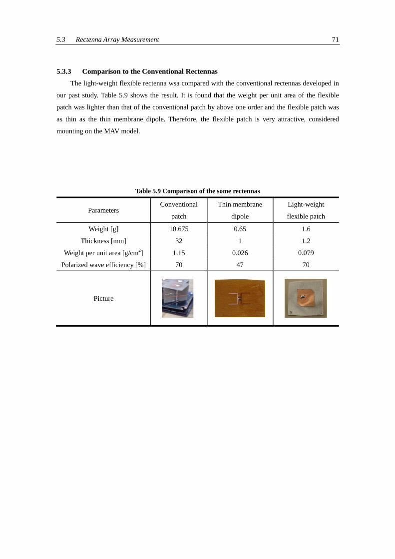
5.3 Rectenna Array Measurement 71
5.3.3 Comparison to the Conventional Rectennas
The light-weight flexible rectenna wsa compared with the conventional rectennas developed in
our past study. Table 5.9 shows the result. It is found that the weight per unit area of the flexible
patch was lighter than that of the conventional patch by above one order and the flexible patch was
as thin as the thin membrane dipole. Therefore, the flexible patch is very attractive, considered
mounting on the MAV model.
Table 5.9 Comparison of the some rectennas
Parameters Conventional
patch
Thin membrane
dipole
Light-weight
flexible patch
Weight [g] 10.675 0.65 1.6
Thickness [mm] 32 1 1.2
Weight per unit area [g/cm2] 1.15 0.026 0.079
Polarized wave efficiency [%] 70 47 70
Picture

5.4 MAV Model Demonstration 72
5.4 MAV Model Demonstration
5.4.1 Parallel Connection of Rectenna
We can treat the rectenna elements as DC power supplies because the RF is converted to the DC
by the diodes. Therefore, we can connect them each other in series and in parallel. The output
voltage is increase with connecting them in series, and the output current does in parallel. By
combining the method of the series connection and of the parallel one suitably according to the
system, we can make the best use of the obtained power. We should prefer the parallel connection
because of the report that the power combining loss with the parallel connections was smaller than
with the series connection[30]
.
The rectenna’s optimized resistance was 100However, the internal resistance of the motor
for the MAV model was 4. Then 10 elements of the rectenna were arrayed in parallel to the motor
as in Figure 5.20. Due to the parallel connection, the optimized resistance of each rectenna was
reduced to 10. In addition, the input power to the motor increased because of the parallel
connection.
Figure 5.20 Schematic of Parallel Connection of Rectenna

5.4 MAV Model Demonstration 73
5.4.2 Total Efficiency in Receiving System
The total efficiency in the receiving system is shown as a product of some efficiency of each
component. Figure 5.21 shows the schematic of the receiving system. The total efficiency is
expressed as:
conversionreturnlosswavepolarizedsystemreceiving . (5.4)
Although polarized wave was average 0.7 and retrunloss is 0.99, conversion changes with the input power.
Then, the total efficiency was calculated for the demonstration at 1500mm height from the horn
antennas. At 1500mm height, since the rectenna could receive average 10mW RF power to the
rectifier circuit (the input power to rectenna was 14.4mW) the conversion efficiency of the rectifier
circuit was 28.1%. Therefore, the total efficiency in receiving system was calculated as 19.5%,
receiving system ~ 0.195, and the DC power received by one rectenna was calculated as 2.81mW at
1500mm height from the transmission system.
Figure 5.21 Schematic of Total Efficiency in Receiving System

5.4 MAV Model Demonstration 74
5.4.3 MAV Model Demonstration
I tested the running the electric motor (4 load) and 10 load, and measured the output voltage
and the DC power. Figure 5.22 shows the result when the MAV model circled 1500mm over the
transmission system. The MAV position was tracked at all times by the tracking system and
microwave beam was transmitted to the MAV at any time by the transmission system. As can be
seen from the figure, the each rectenna element mounted on the MAV converted the microwave
beam into average 1.8mW (at 10 load) or 1mW (at 4 load) DC power. Therefore, the MAV could
receive average 18mW DC power (at 10 load) or 10mW DC power (at 4 load). This result is
different from the calculated result discussed in previous section 5.4.2. It is assumed that the
difference is caused by the tracking error. Because of this, the microwave beam power, in this
experiment, was less than the power calculated.
However, the 18mW and 10mW DC power were enough to move the electric motor. Therefore,
I succeeded to run the electric motor and demonstrate the MAV model mounting the Light-Weigh
Flexible Rectennas.
0
10
20
30
40
0 90 180 270 360
10 load (10 elements)10 load4 load (10 elements)
4 load
DC
pow
er
[mW
]
Angle [deg.]
Figure 5.22 DC Power related to Angle

6.1 Conclusions 75
Chapter 6
Conclusions This chapter shows the conclusions of my study, the perspectives and the issues in the future.
6.1 Conclusions
Some experimental studies on Light-Weight Flexible Rectenna in microwave wireless power
transmission were conducted by the measurement of the efficiency and the properties. The
conclusions are summarized as follows:
1. Light-Weight Flexible Rectennas were developed and it was found that the rectennas were
not inferior to regular rectennas which were on hard dielectrics. In addition, in case of a
mounting on a MAV, it is concluded that the light-weight flexible rectennas are very useful.
2. It was found that the antenna’s polarized wave efficiency was average 70% related to the
antenna’s yaw angel.
3. It was seen that the antenna’s return loss was about -20dB (efficiency was 99%) and the
antenna efficiency of the rectennas declined 5% with 45-degree bent and 10% with 90-degree
bend.
4. It was found that the conversion efficiency of the RF-DC conversion circuit was maximum
58% at 60mW RF power and 100Ω load resistance, and the efficiency didn’t decline with
B-plane bend and declined with A-plane bend degrees.
5. It was concluded that the optimum array pitch of these rectennas was 0.85.
6. I demonstrated our MAV system and succeeded in driving the motor mounted on the MAV
model.

6.2 Future Perspectives and Issues 76
6.2 Future Perspectives and Issues
The rectennas developed in this study have a possibility of improvement of the efficiency since
it is felt that the polarized wave efficiency and the conversion efficiency has not been optimized yet.
In addition, if a high quality Schottky Barrier diode is developed, the conversion efficiency surely
becomes higher. Moreover, I designed the antennas by calculation based on the theory. However, I
find there is still room for improvement in the position of the RF feeding point and the side length.
In the future study, we should optimize the parameters with the analytical results from the computer
simulations of the electromagnetic field, and actually confirm the improvement with the
experiments.
In addition, though the small DC power was converted to in this experiment, the lager power
will be converted to by combinations of the rectennas. Therefore, lager systems will be demonstrated
and developed in the future than our MAV model system.
Finally, it was very difficult to mount rectennas on flying objects due to the rectenna’s weight
and hardness. However the light-weight flexible rectennas got over the problem, so it is expected
that the rectennas are applied to many applications. Therefore, in our laboratory, we will apply them
to spacesuits and so on, and develop new system in Microwave Wireless Power Transmission.

References 77
References
[1] H. Kuwano: “Trends of Energy Harvesting Technologies,” CMC Publishing Co., Ltd
(2010)
[2] H. Matsuki: “Frontier of Wirelesses Electric Power Transmission,” CMC Publishing Co., Ltd
(2009)
[3] A. Kurs, A. Karalis, R. Moffatt, J.D. Joannopoulos, P. Fisher, M. Soljacic: “Wireless Power
Transfer via Strongly Coupled Magnetic Resonances,” Science, 317, pp. 83-86 (2007)
[4] N. Kawashima: “Importance of the Development of a Rover for the Direct Confirmation of
the Existence of Ice on the Moon,” Trans. Jap. Soc. Aeronaut. Space Sci., 43, pp. 33-35
(2000)
[5] 松本 紘,篠原 真毅:“宇宙太陽光発電所とマイクロ波エネルギー伝送技術,”信学
技報 SAT95-77, 95, 443, pp.31-36 (1995)
[6] Brown W. C.: “A survey of the elements of power transmission by microwave beam,” 1961
IRE Int. Convention Record 9, 93-105 (1961)
[7] Brown W. C.: “THE HISTORY OF WIRELESS POWER TRANSMISSION,” Solar Energy
Vol. 56, No. 1 pp 3-21 (1996)
[8] R. Ozawa, “Development of Microwave Energy Supply System,” Master thesis, University
of Tokyo (2007)
[9] K. Katsunaga: “Developments of Polarity-Free Rectenna for Micro Aerial Vehicles,” Master
thesis, University of Tokyo (2007)
[10] S. Komatsu., K. Katsunaga, R. Ozawa, K. Komurasaki and Y. Arakawa: “Power
Transmission to a Micro Aerial Vehicle, AIAA paper 2007-1003 (2007)
[11] E. Shimane., S. Komatsu, K. Komurasaki and Y. Arakawa: “A MAV Flight using Microwave
Power Supply,” AIAA paper 2008-1149 (2008)
[12] D. Takahashi: “Development of light, flexible microwave receipt rectenna,” Bachelor thesis,
University of Tokyo (2008)

References 78
[13] H. Sawahara, A. Oda, A. Diallo, K. Komurasaki, Y. Arakawa: “Power Beaming to a Micro
Aerial Vehicle using an Active Phased Array,” SPIE Smart Structures and Materials +
Nondestructive Evaluation and Health Monitoring, SPIE7674, 76460S (2010)
[14] A. Oda, H. Sawahara, M. Ishiba, K. Komurasaki, Y. Arakawa: “Integration of MAV Wireless
Power Transmission Systems,” 8th
Annual International Energy Conversion Engineering
Conference, 771079 (2010)
[15] M. Ishiba, A. Oda, H. Sawahara, K. Komurasaki, Y. Arakawa: “Wireless Communication
and Power Transmission for a MAV flight,” 2010 Asia-Pacific International Symposium on
Aerospace Technology, 10YS429 (2009)
[16] David M. Pozar: “Microwave Engineering second edition,” Wiley (1997)
[17] Robert S. Elliott: “Antenna Theory and Design Revised Edition,” Wiley-IEEE Press (2003)
[18] T. Yoo, K. Chang: “Theoretical and Experimental Development of 10 and 35 GHz
rectennas,” IEEE Trans. Microwave Theory and Tech., Vol.40, No.6 (1992)
[19] 電子情報通信学会:“アンテナ工学ハンドブック,”オーム社 (2001)
[20] 羽石 操,平澤 一紘,鈴木 康夫:“小型・平面アンテナ,”電子情報通信学会 (1996)
[21] 後藤 尚久:“アンテナ工学入門講座,”電波新聞社 (2008)
[22] R. J. Gutmann and J. M. Borrego: “Power Combining in an Array of Microwave Power
Rectifiers,” IEEE Trans. Microwave Theory and Tech., Vol. MTT-27, pp. 958-968 (1979)
[23] R. J. Gutmann and J. M. Borrego: “Solar power satellite rectenna design study: directional
receiving elements and parallel-series combining analysis,” NASA Final Rep. NAS9-15453,
Ch. 3 (1978)
[24] 谷口 慶治:“マイクロ波電子回路―設計の基礎―,”共立出版 (2004)
[25] J. O. Mcspadden, T. Yoo and K. Chang: “Theoretical and Experimental Investigation of a
Rectenna Element for Microwave Power Transmission,” IEEE Trans. Microwave Theory
and Tech., Vol. 40, pp. 2359-2366 (1992)
[26] J. O. Mcspadden, L. Fan, K. Chang: “Design and Experiments of a
High-Conversion-Efficiency 5.8GHz Rectenna,” IEEE Trans. Microwave Theory and Tech.,
Vol. 46, pp. 2053-2060 (1998).
[27] 田中 正人,張 宰赫:“ウェアラブルパッチアンテナ,”信学技報 AP2002-76 (2002)
[28] 山本 綱之,藤森 和博,佐薙 稔,野木 茂次,真田 篤志:“RF-DC 変換回路の変換
効率に対するダイオードの接合容量の影響,”信学技報 WPT2010-11 (2010)
[29] 篠原 真毅,岡田 寛,三谷 友彦,松本紘:“マイクロ波エネルギー伝送用レクテナ
整流回路のパラメータ最適化に関する研究,”第 24 回宇宙エネルギーシンポジウム
講演論文集 pp.125-129 (2005)
[30] 三浦 健史, 篠原 真毅, 松本 紘: “マイクロ波電力伝送用レクテナ素子の接続法に関
する実験的研究,” 電子情報通信学会論文誌 B, Vol. J82-B, No.7, pp.1374-1383 (1999)

Accomplishments 79
Accomplishments
Conference Presentations
学会発表
[i] ○澤原弘憲,小田章徳,,ディアロ・アルセニー,小紫公也,荒川義博
「MAV 用 5.8GHz レクテナの開発」
第 29 回宇宙エネルギーシンポジウム,相模原,2009 年 2 月
[ii] *Sawahara H., Oda A., Diallo A., Komurasak K., Arakawa Y.
“Power Beaming to a Micro Aerial Vehicle using an Active Phased Array”
SPIE Smart Structures and Materials + Nondestructive Evaluation and Health Monitoring
SPIE7646, 76460S, San Diego, USA, March, 2010
[iii] ○澤原弘憲,小田章徳, 石場舞,石田準,小紫公也,荒川義博,田中孝治
「フレキシブルレクテナの開発」
第 54 回宇宙科学技術連合講演会,1S15,静岡,2010 年 10 月
[iv] ○澤原弘憲,小田章徳,石場舞,小紫公也,荒川義博,田中孝治
「軽量フレキシブルレクテナ搭載 MAV へのマイクロ波自動追尾送電」
第 30 回宇宙エネルギーシンポジウム,相模原,2011 年 2 月

Accomplishments 80
Conference Papers and Journals
学会誌掲載
[a] 高橋大祐,○澤原弘憲,小田章徳,ディアロ・アルセニー,小紫公也,田中孝治,
藤野義之
「軽量フレキシブルレクテナ搭載マイクロ飛行機への無線電力伝送」
電気情報通信学 信学技報 SPS2009-04 (2009 年 7 月)
[b] ○澤原弘憲,小田章徳,,ディアロ・アルセニー,小紫公也,荒川義博
「MAV 用 5.8GHz レクテナの開発」
第 29 回エネルギーシンポジウム 講演論文集 (2010 年 2 月)
[c] *Sawahara H., Oda A., Diallo A., Komurasak K., Arakawa Y.,
“Power Beaming to a Micro Aerial Vehicle using an Active Phased Array”
SPIE Smart Structures and Materials Internet Proceedings (2010 年 3 月)
[d] ○澤原弘憲,小田章徳, 石場舞,石田準,小紫公也,荒川義博,田中孝治
「フレキシブルレクテナの開発」
第 54 回宇宙科学技術連合講演会 講演論文集 (2010 年 10 月)
[e] ○澤原弘憲,小田章徳,石場舞,小紫公也,荒川義博,田中孝治
「軽量フレキシブルレクテナ搭載 MAV へのマイクロ波自動追尾送電」
第 30 回エネルギーシンポジウム 講演論文集 (2011 年 2 月)
[f] ○澤原弘憲,小田章徳,石場舞,石田準,勝永健太,小澤亮二,小松周平,嶋根愛
理,高橋大祐,小紫公也,荒川義博,田中孝治,佐々木進
「軽量フレキシブルパッチレクテナの開発」
電気情報通信学会誌 (投稿中)