Embed Size (px)
Citation preview

Article
Co-Design Method and Wafer-Level PackagingTechnique of Thin-Film Flexible Antenna and SiliconCMOS Rectifier Chips for Wireless-Powered NeuralInterface Systems
Kenji Okabe 1, Horagodage Prabhath Jeewan 1, Shota Yamagiwa 1, Takeshi Kawano 1,Makoto Ishida 1,2 and Ippei Akita 1,*
Received: 9 October 2015; Accepted: 14 December 2015; Published: 16 December 2015Academic Editor: Hung Cao
1 Department of Electrical and Electronic Information Engineering, Toyohashi University of Technology,Aichi 441-8580, Japan; [email protected] (K.O.); [email protected] (H.P.J.);[email protected] (S.Y.); [email protected] (T.K.); [email protected] (M.I.)
2 Electronics-Inspired Interdisciplinary Research Institute (EIIRIS), Toyohashi University of Technology,Aichi 441-8580, Japan
* Correspondence: [email protected]; Tel.: +81-532-44-6746 (ext. 6746); Fax: +81-532-44-6757
Abstract: In this paper, a co-design method and a wafer-level packaging technique of a flexibleantenna and a CMOS rectifier chip for use in a small-sized implantable system on the brain surface areproposed. The proposed co-design method optimizes the system architecture, and can help avoid theuse of external matching components, resulting in the realization of a small-size system. In addition,the technique employed to assemble a silicon large-scale integration (LSI) chip on the very thinparylene film (5 µm) enables the integration of the rectifier circuits and the flexible antenna (rectenna).In the demonstration of wireless power transmission (WPT), the fabricated flexible rectenna achieveda maximum efficiency of 0.497% with a distance of 3 cm between antennas. In addition, WPT withradio waves allows a misalignment of 185% against antenna size, implying that the misalignment hasa less effect on the WPT characteristics compared with electromagnetic induction.
Keywords: wireless power transmission; wafer-level packaging; flip-chip bonding; flexiblesubstrate; rectenna
1. Introduction
Advances in techniques employed in wireless sensor systems have enabled the creation of novelbiomedical applications [1,2]. In particular, neural interface systems including micro-electrode arraysand signal processing circuits have been studied to identify human brain functions based on the weakelectrical signals caused by the activity of nerve cells in the brain [3–10]. The signals obtained fromthe neural interface are essential for realizing brain-machine interfaces and supporting the lack ofinformation in the brain caused by disorders and diseases. However, neural recording systems thatuse wire lines to connect the implanted device to an external device can cause infections through theopening in the skull and the dura. Although the skull is typically be sealed with cement after surgery,it would be difficult to hold the wire and the dura. As a result, there is a risk of infection and leakageof the cerebrospinal fluid during long-term measurement. Therefore, using fully implantable neuralinterfaces are necessary to solve this problem [11–17].
For realizing wireless communication and power transmission to the implanted neural interfaceon the brain surface, several technologies that integrate passive components (e.g., an antenna on aflexible film) with high-performance active circuits have been studied [18–22]. In particular, many
Sensors 2015, 15, 31821–31832; doi:10.3390/s151229885 www.mdpi.com/journal/sensors

Sensors 2015, 15, 31821–31832
functional circuits including amplifiers, analog-to-digital converters, signal processors, and RF circuitsare needed and they should all support low-power operation [23–33]. Very thin film flexible transistorsfabricated with organic or bio-resorbable materials can be used to fabricate monolithic film deviceswith passive and active components. However, these flexible transistors require a large area for themulti-functional circuits because the gate size of the transistors exceeds 15 µm caused by evaporationthrough a shadow mask [18]. Therefore, implementing highly integrated systems using flexibletransistors might be difficult. As an alternative, fabrication processes that integrate a complementarymetal-oxide semiconductor (CMOS) IC on a flexible substrate have been developed [19–23]. Althoughthe mounting method based on a micro electro-mechanical system (MEMS) technology enables accuratealignment in the integration of the CMOS IC chip and the flexible film device, this alignment becomeschallenging when mounting several chips on the same film [19,20]. To overcome this challenge,a mounting technique using the flip-chip bonding method has been studied. This method can helpachieve good alignment even if several chips are packaged on a flexible substrate [21,22]. A polyimidefilm and a CMOS IC chips have also been integrated using flip-chip bonding technology [21]. Becausethis polyimide film has a certain thickness, the fabricated device exhibited sufficient flexibility andhardness, making it suitable to be implanted on the surface of the eyeball. However, the neuralinterface implanted on the brain surface requires that the flexible film be thinner in order to fit theshape of the brain [6]. Therefore, there is a need for a technique that can be used for mounting CMOSIC chips on a very thin film device.
The design methodology of RF circuits is also important to realize such small-size implantabledevices. In the wireless power transmission (WPT) device, an inductance element is generally requiredfor matching the impedance between an antenna and a rectifier [23], that is, external components arerequired. Considering the size constraint of the implantable device, a design method that eliminatessuch matching components should be considered. Although [24] achieves a small inductance formatching impedance by using an inductive antenna, it is difficult to apply in implantable devicesbecause this antenna is relatively large and thick, 50 mm ˆ 43 mm ˆ 0.5 mm. Therefore, an antenna anda rectifier (rectenna) co-design method must be considered to reduce the use of matching componentsand miniaturize the antenna size.
In this paper, we propose a co-design method and an assembly technique of a flexible antenna andthe CMOS rectifier chip for realizing small-sized implementation of implantable neural interfaces. Theadvantages of the proposed technique are that it does not require any off-chip matching componentsbetween the antenna and the rectifier, and it allows integration of a high-performance silicon chip onan ultra-thin flexible film with a thickness of 10 µm. For minimizing the size of the implantable device,the antenna is designed to have a small inductance to avoid using additional matching componentsbetween the antenna and the rectifier. Furthermore, an on-chip transformer preceding the rectifiercan reduce the inductance, resulting in a smaller inductive antenna device. In addition, we havedeveloped a wafer-level packaging technique for mounting the CMOS IC chip on a thin film withflip-chip bonding. To the best of our knowledge, an assembly technique on a thin film with a thicknessof 5 µm has never been reported in the past. Although a previous study [34] by the authors reported asilicon CMOS rectifier chip mounted on the antenna with the flexible substrate and demonstrated WPT,detailed design methodologies and discussions were not provided. This paper presents additionalinformation on an impedance matching method and analysis, the flip-chip bonding process, andadditional measurement results and discussion for realizing small-sized devices.
The remainder of this paper is organized as follows: in Section 2, we present the architecture andthe co-design method of the flexible rectenna that contains a flexible antenna, an on-chip transformer,and a CMOS rectifier for impedance matching. Section 3 explains the fabrication process for theflexible device, especially the flip-chip bonding technology to connect a silicon chip. In Section 4, wedemonstrate WPT by the fabricated device, and discuss the power transfer efficiency by comparingthe measured and calculated results. Finally, conclusions are provided in Section 5.
31822

Sensors 2015, 15, 31821–31832
2. Flexible Rectenna Device
2.1. Architecture of the Implantable Device
The proposed architecture of the flexible device implanted on the brain surface is shown in Figure 1.Highly functional active circuits are implemented in a silicon chip that is embedded in a flexible film.Some passive components, including the antenna and the electrode array, are also patterned in the flexiblefilm. A thin parylene film is selected as the flexible material because of its good flexibility, which allows itto fit the brain surface, and its high biocompatible. In this paper, as a WPT part is considered, a co-designmethodology of circuits and the antenna is needed for achieving the optimum design in terms of devicesize and performance, and the methodology is described in the next section.
Figure 1. Proposed architecture of the flexible device for wireless-powered neural interface systems.
2.2. Co-Design Methodology
Figure 2 shows the circuit diagram of the flexible rectenna designed for WPT. The flexible rectennahas three parts: a flexible antenna having a small inductance, an on-chip transformer for matching theimpedance between the antenna and the rectifier, and a rectifier circuit. In this schematic, the antennais made of metal in the parylene film and the other parts are implemented in a 180-nm standard CMOSprocess. The rectifier circuit is formed by cascading in three stages and it has charge pump capabilityfor DC–DC conversion [35]. To design the on-chip transformer between a 50-W terminated antenna andthe CMOS rectifier, the input impedance of the rectifier should be calculated assuming that the MOStransistor is switched on. The received antenna would be able to receive about 700 µW (´1.54 dBm),which is determined by available received power on the human brain [17]. Therefore, the gate size ofMOS transistors in the rectifier and the on-chip transformer were designed to match the impedanceof rectifier and antenna when the received power is 700 µW. The ratios of the gate width to the gatelength (W/L) for n-MOS and p-MOS transistors are 66.6 and 200, respectively, and the threshold voltage(VTH) is approximately 350 mV. The CMOS rectifier is activated when a voltage greater than 350 mV isapplied to the RF terminals that are connected to the antenna elements. The on-resistance of the MOStransistor (RON) is calculated as:
RON “ 1� pVGS ´ VTHq (1)
where b is the parameter decided by the W/L ratio, the carrier mobility, and the unit capacity of gate,and VGS is the gate-to-source voltage. Equation (1) indicates that RON depends on the input powerbecause VGS is determined by the transmitted power from the antenna to the CMOS rectifier. Therefore,a certain level of input power range into the rectifier should be defined in order to specify RON . In thecase of the designed CMOS rectifier circuit, the real part of the input impedance varies from 100 Wto 650 W, when the input power is sufficiently high. Consequently, the on-chip transformer shouldbe designed to have a turn ratio of 1:3, implying that the real-part input impedance of antenna isseen as 450 W from the rectifier side. The on-chip transformer with silicon substrate is designed witha turns ratio of 2:6 and size of 800 µm ˆ 800 µm with an electromagnetic simulator (Momentum,Keysight Technologies, Santa Rosa, CA, USA). The width and space of the coil are 4 µm and 3 µm,respectively, and the self-resonant frequency is higher than 3 GHz in this design. The transformer
31823

Sensors 2015, 15, 31821–31832
has maximum efficiency at a frequency of 825 MHz when the outer diameter of the transformer isadjusted to 800 µm. The transfer characteristic of the designed transformer is approximately ´3.4 dBat the frequency of 825 MHz. In addition, some inductance components are required for matching theimpedance between the antenna and the rectifier because the rectifier has capacitive impedance. Thisunintended negative reactance can be cancelled using an inductance of 3.4 nH, which can be easilyadded in the antenna design. Thus, the flexible antenna having a small inductance can help eliminatethe need for using extra inductance components.
Figure 2. Circuit schematic of the proposed WPT device: The antenna with inductance can helpeliminate the need for using external matching components, thus facilitating a reduction in the size ofthe neural interface device.
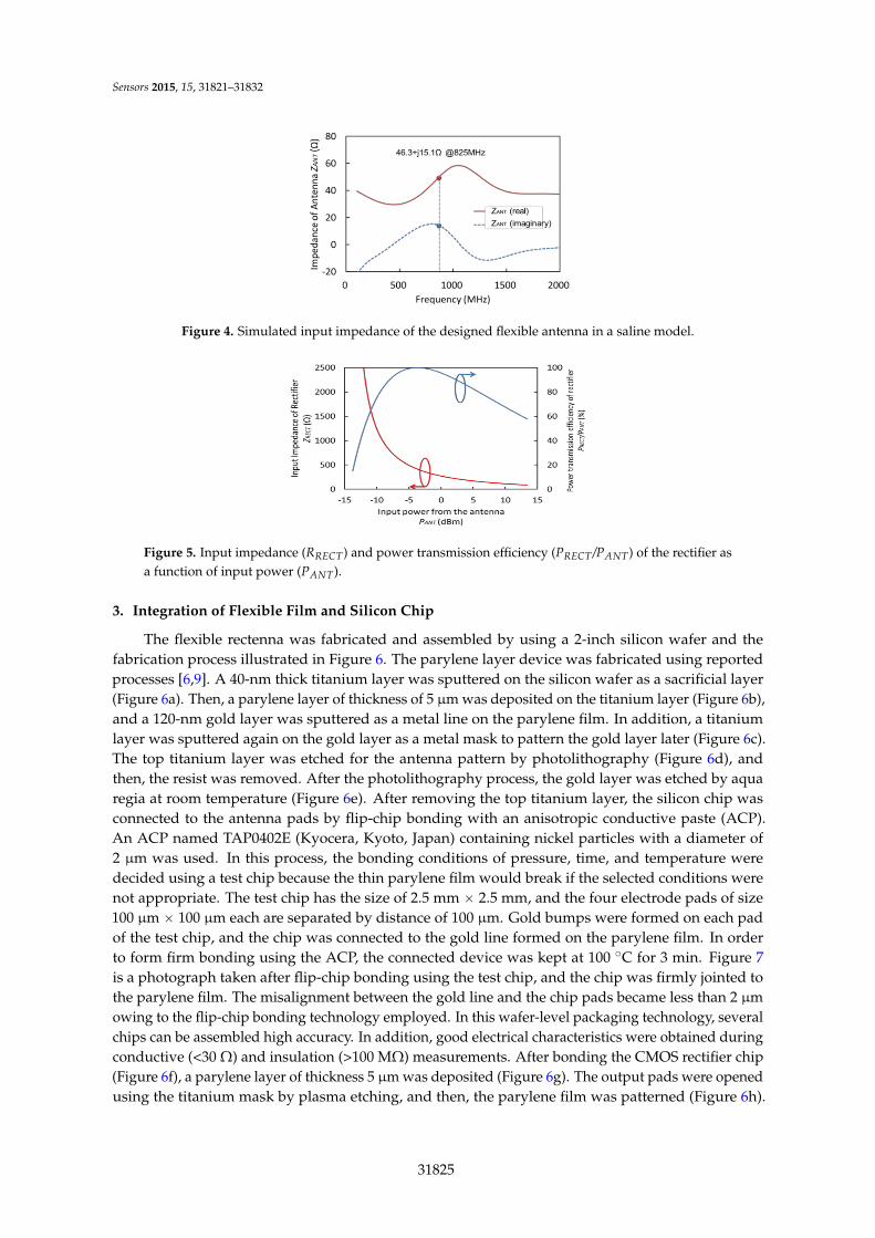
The structure of the flexible and inductive antenna is based on a dipole antenna model and theantenna is designed using an electromagnetic simulation engine (EMPro, Keysight Technologies).The model of dipole antenna was adopted in order to form on the flexible film in plane. The antennawas designed on the flexible film with a large area of 27 mm ˆ 5 mm, as the gain of the antennadepends directly on its size. The flexible antenna is analyzed in a saline model that represents thebrain tissue. Figure 3 shows the diagram of the designed flexible antenna with the CMOS rectifierchip. The antenna’s metal line is patterned using gold, with a width of 1 mm and thickness of 120 nm.The flexible film has a size of 27 mm ˆ 5 mm ˆ 10 µm, and the assembled silicon chip has a thicknessof 400 µm. 97% of the device area is composed of a flexible film, as the silicon chip has a small areaof 1.5 mm ˆ 2.5 mm only. The simulated input impedance of the antenna is shown in Figure 4 andit indicates an impedance of 46.3 + j15.1 W at 825 MHz, indicating that the designed antenna has aninductance of 3 nH. From these simulation results, the power ratio, defined as the input power into therectifier (PRECT) divided by the transmitted power from the antenna (PANT), is estimated as:
PRECTPANT
“ 4¨ZANT¨ZRECT
pZANT ` ZRECTq2 (2)
where ZANT and ZRECT are the input impedances of the antenna and the rectifier, respectively. ZRECTdepends on the gate voltage as described previously. Figure 5 shows the input impedance of therectifier (ZRECT) and the efficiency of power transmission to the rectifier from the antenna (PRECT/PANT)versus the input power from the antenna (PANT). The power loss due to impedance mismatch is lessthan ´1.0 dB in the range of the input power from ´10 to 5 dBm.
Figure 3. Diagram of the designed flexible antenna with the CMOS rectifier chip.
31824
Sensors 2015, 15, 31821–31832
Figure 4. Simulated input impedance of the designed flexible antenna in a saline model.
Figure 5. Input impedance (RRECT) and power transmission efficiency (PRECT/PANT) of the rectifier asa function of input power (PANT).
3. Integration of Flexible Film and Silicon Chip
The flexible rectenna was fabricated and assembled by using a 2-inch silicon wafer and thefabrication process illustrated in Figure 6. The parylene layer device was fabricated using reportedprocesses [6,9]. A 40-nm thick titanium layer was sputtered on the silicon wafer as a sacrificial layer(Figure 6a). Then, a parylene layer of thickness of 5 µm was deposited on the titanium layer (Figure 6b),and a 120-nm gold layer was sputtered as a metal line on the parylene film. In addition, a titaniumlayer was sputtered again on the gold layer as a metal mask to pattern the gold layer later (Figure 6c).The top titanium layer was etched for the antenna pattern by photolithography (Figure 6d), andthen, the resist was removed. After the photolithography process, the gold layer was etched by aquaregia at room temperature (Figure 6e). After removing the top titanium layer, the silicon chip wasconnected to the antenna pads by flip-chip bonding with an anisotropic conductive paste (ACP).An ACP named TAP0402E (Kyocera, Kyoto, Japan) containing nickel particles with a diameter of2 µm was used. In this process, the bonding conditions of pressure, time, and temperature weredecided using a test chip because the thin parylene film would break if the selected conditions werenot appropriate. The test chip has the size of 2.5 mm ˆ 2.5 mm, and the four electrode pads of size100 µm ˆ 100 µm each are separated by distance of 100 µm. Gold bumps were formed on each padof the test chip, and the chip was connected to the gold line formed on the parylene film. In orderto form firm bonding using the ACP, the connected device was kept at 100 ˝C for 3 min. Figure 7is a photograph taken after flip-chip bonding using the test chip, and the chip was firmly jointed tothe parylene film. The misalignment between the gold line and the chip pads became less than 2 µmowing to the flip-chip bonding technology employed. In this wafer-level packaging technology, severalchips can be assembled high accuracy. In addition, good electrical characteristics were obtained duringconductive (<30 W) and insulation (>100 MW) measurements. After bonding the CMOS rectifier chip(Figure 6f), a parylene layer of thickness 5 µm was deposited (Figure 6g). The output pads were openedusing the titanium mask by plasma etching, and then, the parylene film was patterned (Figure 6h).
31825

Sensors 2015, 15, 31821–31832
Finally, by etching the sacrificial titanium layer, the parylene film with the chip was released from thesilicon wafer (Figure 6i).
Figure 6. Fabrication process of flexible rectenna mounting the CMOS rectifier chip with the transformeron the parylene film.
Figure 7. Photograph after flip-chip bonding process (Figure 6f).
Figure 8 shows the fabricated parylene film device and the bonded on-chip full wave CMOSrectifier with the transformer. The size of the flexible device is 27 mm ˆ 5 mm and it has a goodflexibility. The CMOS rectifier chip of size 1100 µm ˆ 840 µm has four pads for providing rectifiedoutput voltage, GND, and the RF signal terminals.
Figure 8. Photographs of the fabricated flexible rectenna and the bonded CMOS rectifier chip withthe transformer.
4. Measured Results and Discussion
As the fabricated rectenna device is designed for use on the brain surface, the performance of thedevice was measured in a saline model that served as the emulation of the implant [19]. Figure 9 showsthe experimental setup with the saline tank (0.9% NaCl solution) in an anechoic chamber. First, an antennadevice without a rectifier was evaluated to characterize the flexible antenna, and its input impedance of41.2 + j44.3 W was observed at the resonance frequency of 825 MHz. In this case, the measured returnloss was ´7.02 dB. The fabricated antenna had a gain of ´20.5 dBi in the direction of Z-axis, a value that
31826

Sensors 2015, 15, 31821–31832
matches well with the simulated result of ´20.9 dBi as shown in Figure 10. Therefore, the simulation canestimate the reasonable antenna gain as it includes the influence of a saline environment, thus facilitatingthe measurement of the total efficiency of the WPT system. For example, the free-space loss is 10.8 dB at afrequency of 825 MHz and at a distance of 10 cm between each antenna. Therefore, the WPT efficiencybetween each antenna can be estimated to be ´29.6 dB, if the gains of the transmission dipole antenna andthe receiver antenna are 2.14 dBi and ´20.9 dBi respectively.
Figure 9. Measurement setup for WPT demonstration using saline tank in anechoic chamber.
Figure 10. Radiation characteristics of fabricated flexible antenna immersed in saline tank.
We demonstrated WPT using the flexible rectenna that integrates the flexible antenna and theCMOS rectifier chip with the transformer. The RF power at 825 MHz was transmitted using a standardhalf-wavelength dipole antenna at a distance of D from the flexible antenna. The load resistance ROUTandthe load capacitance COUT were connected to the output port of the rectifier. Figure 11 shows the observedrectifier output voltage waveform when D = 10 cm, the input power was 18 dBm, and the load resistanceand load capacitance were 17.3 kW and 100 µF, respectively. The output capacitor was charged up whenthe RF signal was input and it was confirmed that the output voltage increased to 970 mV after 18 s.
Figure 11. Measured output voltage waveform of the rectifier in WPT.
31827

Sensors 2015, 15, 31821–31832
Figure 12a–c show the output voltage, the output power, and the total efficiency versus the inputpower of the transmission antenna at distances 3, 5, 10, and 15 cm, respectively. The output resistancewas adjusted to maximize the total efficiency such that the output voltage did not exceed 1.5 V, asshown in Figure 12a. The output voltage and the output power decreased as the distance betweenthe antennas becomes longer. In these measurement results, the maximum efficiency was 0.497% ata distance of 3 cm and input power of 8 dBm, and the efficiency obtained compares well with thecalculated value of 0.36%. The solid lines in Figure 12c depict the theoretical efficiencies which arecalculated using the block diagram of the WPT system shown in Figure 13. The total efficiency, h (%),is calculated as:
h “ POUTPIN
ˆ 100 “ GTX¨LSPACE¨GRX¨LTRANS¨LMATCH¨hRECT (3)
where PIN and POUT are the input power of the transmission antenna and the output power consumedin load resistor ROUT , respectively. GTX and GRX are antenna gains of transmission and reception,LSPACE is the free space loss, LTRANS is the transformer loss, LMATCH is the mismatch loss calculatedby Equation (2), and hRECT is the efficiency of the CMOS rectifier. The free-space loss can be calculatedby the Friis transmission equation as:
LSPACE “ 10¨log10
ˆl
4pD
˙2(4)
where D is the distance and l is the wave length. The calculated power efficiency from Equation (3)has similar curves compared with measured values as shown in Figure 12c. The peak of total efficiencycharacteristics depends on the input power into the flexible antenna (PANT), which is determinedby PIN , GTX, GRX, and LSPACE. Therefore, the characteristic of the total efficiency is affected by thecharacteristic of LMATCH determined by PIN and distance between each antenna.
(a) (b) (c)
Figure 12. Measured output voltage (VOUT), output power (POUT), and total efficiency (h) versus inputpower (PIN) for different distances (D). (a) VOUT versus input power; (b) POUT versus input power;(c) h versus input power.
Figure 13. Block diagram of the WPT system.
The frequency characteristics of the total efficiency for different positions of the transmissionantenna are shown in Figure 14. The peak efficiency was observed at the resonance frequency of825 MHz. Figure 14 also shows the characteristics of efficiency regarding a misalignment in horizontal
31828

Sensors 2015, 15, 31821–31832
and vertical direction when the distance is 5 cm between antennas and there is not misalignment inangle between antennas. The transmission antenna was moved by 5 cm in horizontal and verticaldirection. As a result, the efficiency became 0.21% from 0.24% when the misalignment in horizontaldirection is 5 cm, which is 185% of the fabricated antenna size (27 mm). Comparing with WPTs usingelectromagnetic induction, the misalignment of the implanted coil and the outer devices drasticallyaffects the efficiency. The misalignment of 10% against coil size causes the WPT efficiency to decrease to85% in electromagnetic-induction-based WPTs [36]. By contrast, the fabricated RF-based device allowsthe misalignment of 185% against antenna for the same efficiency reduction of 85%. Therefore, thefabricated device has a tolerance to misalignment between the implanted and outer devices in terms ofWPT efficiency loss. Table 1 shows the comparison results of the WPT devices [37,38]. Although themethod by radio waves has a lower power efficiency compared to electromagnetic induction, it has theadvantages of long distance WPT, and it also allows for some misalignment between the implantedand outer devices. As seen from Figure 12c, the fabricated rectifier outputs the power (POUT) of 22 µWwhen D = 5 cm and PIN = 10 dBm. If the misalignment in horizontal direction is 5 cm, the output power(POUT) becomes 19 µW, the value of which is 85% of the power without misalignment. This obtainedpower could drive a neural interface LSI, such as [37] by charging in a battery in temporarily. Forinstance, a battery can be charged with a constant current of several tens of micro amperes (µA) [39].Since the loaded current in the implemented system can be calculated as 27 µA at the condition ofPIN = 10 dBm and VOUT = 700 mV at D = 5 cm, the received power is reasonable to charge a battery.
Figure 14. Frequency response of total efficiency (h) for different positions (D = 5 cm).
Table 1. Comparison of WPT system with existing studies.
Study Method Device Size(Area, Thickness)
TransmissionEfficiency(Tx to Rx)
OperatingFrequency
CommunicationDistance
[37] Electromagnetic induction 6.5 ˆ 6.5 mm2, >5 µm ´17.3 dB 300 MHz 1.6 cm[38] Electromagnetic induction 5 ˆ 5 mm2, >20 µm ´26 dB 118 MHz 4 cm
This work Radio wave 5 ˆ 27 mm2, 10 µm ´29.6 dB 825 MHz 10 cm
5. Conclusions
The co-design and assembly methods of the flexible antenna and the CMOS rectifier chip areproposed for fabricating implantable neural interfaces. The power loss from the flexible antennainto the CMOS rectifier is saved by using a well-designed on-chip transformer for the input powerranging from ´10 to 5 dBm. The presented design method also eliminates the required inductance forimpedance matching, resulting in less components and smaller sizes. The integrated flexible rectennadevice with differential substrates has been fabricated with the flip-chip bonding technique to mountthe silicon chip on the 5-µm thick parylene film. We have achieved to match the impedance of theantenna and the rectifier by using the flexible antenna with a size of 27 mm ˆ 5 mm ˆ 10 µm, andon-chip transformer with an area of 800 µm ˆ 800 µm. The measured maximum efficiency was 0.497%with 3 cm between each antenna. Furthermore, the RF-based WPT allows the misalignment of 185%
31829

Sensors 2015, 15, 31821–31832
against the antenna size while maintaining more than 85% efficiency degradation, indicating thetolerability against a misalignment compared with electromagnetic induction.
Acknowledgments: This work is partially supported by Grants-in-Aid for Scientific Research (A) andYoung Scientists (A) and (B) from the Japan Society for the Promotion of Science and Tailor-Made Baton-ZoneEducation Program from Toyohashi University of Technology. The authors would like to thank the staff andstudents of Toyohashi University of Technology for their helpful support.
Author Contributions: K.O. conceived, designed, fabricated the device, measured and analyzed the data, andwrote the paper; H.P.J. supported fabrication; S.Y., T.K. and M.I. discussed the fabrication process; and I.A.designed and led the project, analyzed the data, and wrote the paper.
Conflicts of Interest: The authors declare no conflict of interest.
References
1. Zhu, Z.; Liu, T.; Li, G.; Li, T.; Inoue, Y. Wearable Sensor Systems for Infants. Sensors 2015, 15, 3721–3749.[CrossRef] [PubMed]
2. Basar, M.R.; Ahmad, M.Y.; Cho, J.; Ibrahim, F. Application of Wireless Power Transmission Systems inWireless Capsule Endoscopy: An Overview. Sensors 2014, 14, 10929–10951. [CrossRef] [PubMed]
3. Nicolelis, M.A.L. Actions from thoughts. Nature 2001, 409, 403–407. [CrossRef] [PubMed]4. Hochberg, L.R.; Serruya, M.D.; Friehs, G.M.; Mukand, J.A.; Saleh, M.; Caplan, A.H.; Branner, A.; Chen, D.;
Penn, R.D.; Donoghue, J.P. Neuronal ensemble control of prosthetic devices by a human with tetraplegia.Nature 2006, 442, 164–171. [CrossRef] [PubMed]
5. Hochberg, L.R.; Bacher, D.; Jarosiewicz, B.; Masse, N.Y.; Simeral, J.D.; Vogel, J.; Haddadin, S.; Liu, J.; Cash, S.S.;Smagt, P.; et al. Reach and grasp by people with tetraplegia using a neurally controlled robotic arm. Nature2013, 485, 372–377. [CrossRef] [PubMed]
6. Yamagiwa, S.; Ishida, M.; Kawano, T. Self-curling and -sticking flexible substrate for ECoG electrode array.In Proceedings of the 26th IEEE International Conference on Micro Electro Mechanical Systems (MEMS),Taipei, Taiwan, 20–24 January 2013; pp. 480–483.
7. Leuthardt, E.C.; Gaona, C.; Sharma, M.; Szrama, N.; Roland, J.; Freudenberg, Z.; Solis, J.; Breshears, J.;Schalk, G. Using the electrocorticographic speech network to control a brain-computer interface in humans.J. Neural Eng. 2011, 8, 1–11. [CrossRef] [PubMed]
8. Donoghue, J.P. Connecting cortex to machines: Recent advances in brain interfaces. Nat. Neurosci. 2002, 5,1085–1088. [CrossRef] [PubMed]
9. Yamagiwa, S.; Ishida, M.; Kawano, T. Flexible parylene-film optical waveguide arrays. Appl. Phys. Lett. 2015,107. [CrossRef]
10. Nguyen, C.M.; Kota, P.K.; Minh, M.Q.; Dubey, S.; Rao, S.; Mays, J.; Chiao, J.C. Wireless power transfer forautonomous wearable neurotransmitter sensors. Sensors 2015, 15, 24553–24572. [CrossRef] [PubMed]
11. Borton, D.A.; Yin, M.; Aceros, J.; Nurmikko, A. An implantable wireless neural interface for recording corticalcircuit dynamics in moving primates. J. Neural Eng. 2013, 10. [CrossRef] [PubMed]
12. Akita, I. Development of low-power analog/RF mixed-signal circuits with flexible thin film devices forwireless BMI systems. In Proceedings of the 2015 IEEE International Symposium on Radio-FrequencyIntegration Technology (RFIT), Sendai, Japan, 26–28 August 2015; pp. 4–6.
13. Baharami, H.; Mirbozorgi, S.A.; Rusch, L.A.; Gossel, B. Biological channel modeling and implantable UWBantenna design for neural recording systems. IEEE Trans. Biomed. Eng. 2015, 62, 88–98. [CrossRef] [PubMed]
14. Mestais, C.S.; Charvet, G.; Starace, F.S.; Foerster, M.; Ratel, D.; Benabid, A.L. Wimagine: Wireless 64-channelECoG recording implant for long term clinical applications. IEEE Trans. Neural Syst. Rehabil. Eng. 2015, 23,10–21. [CrossRef] [PubMed]
15. Fun, D.; Rich, D.; Holtzman, T.; Ruther, P.; Dalley, J.W.; Lopez, A.; Rossim, M.A.; Barter, J.W.; Salas-Meza, D.;Herwik, S.; et al. A wireless multi-channel recording system for freely behaving mice and rats. PLOS ONE2011, 6, e22033. [CrossRef] [PubMed]
16. Muller, R.; Le, H.P.; Li, W.; Ledochowitsch, P.; Gambini, S.; Bjorninen, T.; Koralek, A.; Carmena, J.M.;Maharbiz, M.M.; Alon, E.; et al. A miniaturized 64-channel 225 µW wireless electrocorticographic neuralsensor. In Proceedings of the 2014 IEEE International Solid-State Circuits Conference (ISSCC), San Francisco,CA, USA, 9–13 February 2014; pp. 412–413.
31830

Sensors 2015, 15, 31821–31832
17. Zhao, Y.; Tang, L.; Rennaker, R.; Hutchens, C.; Ibrahim, T.S. Studies in RF Power Communication, SAR, andTemperature Elevation in Wireless Implantable Neural Interfaces. PLOS ONE 2013, 8. [CrossRef] [PubMed]
18. Hwang, S.W.; Huang, X.; Seo, J.H.; Song, J.K.; Kim, S.; Ali, S.H.; Chung, H.J.; Fiorenzo, H.T.; Omenetto, G.;Ma, Z.; et al. Materials for bioresorbable radio frequency electronics. Adv. Mater. 2013, 25, 3526–3531.[CrossRef] [PubMed]
19. Li, W.; Rodger, D.C.; Meng, E.; Weiland, J.D.; Humayun, M.S.; Tai, Y.C. Wafer-level packaging with integratedRF electronics for wireless retinal prostheses. IEEE J. Microelectron. Syst. 2010, 19, 735–742. [CrossRef]
20. Wang, L.; Sterken, T.; Cauwe, M.; Cuypers, D.; Vanfleteren, J. Fabrication and characterization of flexibleultrathin chip package using photosensitive polyimide. IEEE Trans. Compon., Packag. Manuf. Technol. 2012, 2,1099–1106. [CrossRef]
21. Noda, T.; Sasagawa, K.; Tokuda, T.; Kanda, H.; Terasawa, Y.; Tashiro, H.; Fujikado, T.; Ohta, J. Fabrication offork-shaped retinal stimulator integrated with CMOS microchips for extension of viewing angle. Sens. Mater.2014, 26, 637–648.
22. Yim, M.J.; Pail, K.W. Recent advances on anisotropic conductive adhesives (ACAs) for flat panel displaysand semiconductor packaging applications. Int. J. Adhes. Adhes. 2006, 26, 304–313. [CrossRef]
23. Mazzilli, F.; Thoppay, P.E.; Johl, N.; Dehollain, C. Design methodology and comparison of rectifiers forUHF-band RFIDs. In Proceedings of the 2010 IEEE Radio Frequency Integrated Circuits Symposium (RFIC),Anaheim, CA, USA, 23–25 May 2010; pp. 505–508.
24. Stoopman, M.; Keyrouz, S.; Visser, H.J.; Philips, K.; Serdijin, W.A. Co-design of CMOS rectifier and small loopantenna for highly sensitive RF energy harvesters. IEEE J. Solid-State Circuits 2014, 49, 622–634. [CrossRef]
25. Okabe, K.; Akita, I.; Ishida, M. High-gain on-chip antenna using a sapphire substrate for implantable wirelessmedical systems. Jpn. J. Appl. Phys. 2014, 53. [CrossRef]
26. Okazawa, T.; Akita, I.; Ishida, M. A digitally calibrated dynamic comparator using time-domain offsetdetection. Analog. Integr. Circ. Signal Process. 2014, 81, 561–570. [CrossRef]
27. Akita, I.; Ishida, M. A chopper-stabilized instrumentation amplifier using area-efficient self-trimmingtechnique. Analog. Integr. Circ. Signal Process. 2014, 81, 571–582. [CrossRef]
28. Akita, I.; Asai, S.; Ishida, M. Low-power output-capacitorless low-dropout regulator with adjustable chargeinjection technique for on-off-keying transmitters. Jpn. J. Appl. Phys. 2014, 53. [CrossRef]
29. Haibi, H.; Akita, I.; Ishida, M. A 27-nV/‘
Hz 0.015-mm2 three-stage operational amplifier with splitactive-feedback compensation. In Proceedings of the 2013 IEEE Asian Solid-State Circuits Conference(ASSCC), Singapore, 11–13 November 2013; pp. 365–368.
30. Akita, I.; Ishida, M. A 0.06 mm2 14 nV/‘
Hz chopper instrumentation amplifier with automaticdifferential-pair matching. In Proceedings of the 2013 IEEE International Solid-State Circuits Conference(ISSCC), San Francisco, CA, USA, 17–21 February 2013; pp. 178–179.
31. Akita, I.; Itakura, T.; Shiraishi, K. Current-steering digital-to-analog converter with a high-PSRR currentswitch. IEEE Trans. Circuits Syst. II 2011, 58, 724–728. [CrossRef]
32. Akita, I.; Furuta, M.; Matsuno, J.; Itakura, T. A 7-bit 1.5-GS/s time-interleaved SAR ADC with dynamictrack-and-hold amplifier. In Proceedings of the 2013 IEEE Asian Solid-State Circuits Conference (ASSCC),Jeju, Korea, 14–16 November 2011; pp. 293–296.
33. Akita, I.; Wada, K.; Tadokoro, Y. A 0.6-V dynamic biasing filter with 89-dB dynamic range in 0.18-µm CMOS.IEEE J. Solid State Circuits 2009, 44, 2790–2799. [CrossRef]
34. Okabe, K.; Akita, I.; Yamagiwa, S.; Kawano, T.; Ishida, M. A thin film flexible antenna with CMOSrectifier chip for RF-powered implantable neural interfaces. In Proceedings of the Transducers—18thInternational Conference on Solid-State Sensors, Actuators Microsystems, Anchorage, AK, USA, 21–25 June2015; pp. 1751–1754.
35. Kotani, K.; Sasaki, A.; Ito, T. High-efficiency differential-drive CMOS rectifier for UHF RFIDs. IEEE J. SolidState Circuits 2009, 44, 3011–3018. [CrossRef]
36. Soma, M.; Galbraith, D.C.; White, R.L. Radio-frequency coils in implantable devices: Misalignment analysisand design procedure. IEEE Trans. Biomed. Eng. 1987, 4, 276–282. [CrossRef]
37. Muller, R.; Hanh-Phuc, L.; Wen, L.; Ledochowitsch, P.; Gambini, S.; Bjorninen, T.; Koralek, A.; Carmena, J.M.;Maharbiz, M.M.; Alon, E.; et al. A Minimally Invasive 64-Channel Wireless µECoG Implant. IEEE J. SolidState Circuits 2015, 50, 344–359. [CrossRef]
31831

Sensors 2015, 15, 31821–31832
38. Sun, X.; Zheng, Y.; Li, Z.; Li, X.; Zhang, H. Stacked Flexible Parylene-Based 3D Inductors with Ni80Fe20Core for Wireless Power Transmission System. In Proceedings of the 26th IEEE International Conference onMicro Electro Mechanical Systems (MEMS), Taipei, Taiwan, 20–24 January 2013; pp. 849–852.
39. Masuch, J.; Delgado-Restituto, M.; Milosevic, D.; Baltus, P. Co-integration of RF energy harvester into a2.4 GHz transceiver. IEEE J. Solid State Circuits 2013, 48, 1565–1574. [CrossRef]
© 2015 by the authors; licensee MDPI, Basel, Switzerland. This article is an open accessarticle distributed under the terms and conditions of the Creative Commons by Attribution(CC-BY) license (http://creativecommons.org/licenses/by/4.0/).
31832
![[XLS] · Web viewAL3Z AU2Z WPT-1090 BL3Z F4AZ 15A416 9E5Z K WPT-1161 8L3Z F5SZ 9F479 UB WPT-992 8C2Z BHAB WPT-1147 F5TZ AU5Z WPT-1089 16611B08 16611B09 BC3Z F5CZ XF3Z WPT-1001 NUB](https://img.dokumen.tips/doc/110x75/5af9707e7f8b9aac248e66a3/xls-viewal3z-au2z-wpt-1090-bl3z-f4az-15a416-9e5z-k-wpt-1161-8l3z-f5sz-9f479-ub.jpg)