Embed Size (px)
Citation preview

© 2006 Texas Instruments Inc, Slide 1
Leveraging MSP430 for Robust System Design
Lane WestlundMSP430 Applications Engineer
Texas Instruments

© 2006 Texas Instruments Inc, Slide 2
• Startup and Power Supply• ESD• Board Design• Crystal Considerations• Built-in Protection• Software Considerations
Agenda

© 2006 Texas Instruments Inc, Slide 3
Power On Reset (POR)
• Built-into MSP430s w/o brownout reset• Consists of two parts:
Power-on reset detection Power-on reset delay
• Guaranteed POR if VCC ≤ 0.2V and |dV/dt| ≥ 1V/ms• POR is not a voltage supervising circuit!

© 2006 Texas Instruments Inc, Slide 4
POR Operation
• Code execution can start with VCC as low as 0.8V• VPOR is temperature dependent!• Remember: VCCmin = 1.8V• Always obey max. MCLK vs. VCC!
© 2006 Texas Instruments Inc, Slide 5
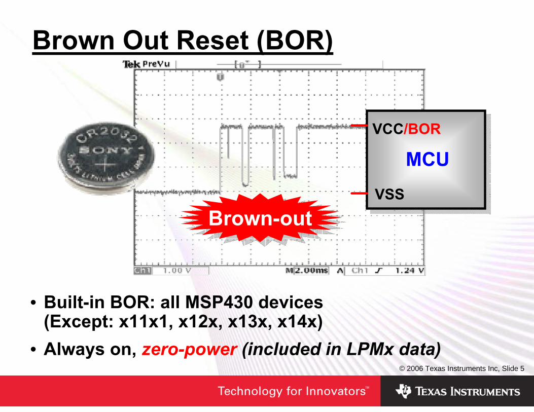
Brown Out Reset (BOR)
• Built-in BOR: all MSP430 devices(Except: x11x1, x12x, x13x, x14x)
• Always on, zero-power (included in LPMx data)
Brown-outBrown-out
VCC/BOR
VSS
MCU

© 2006 Texas Instruments Inc, Slide 6
BOR Operation
• RESET when VCC crosses VCC(Start)
• BOR releases device after VCC = V(B_IT−) + Vhys(B_IT−)and td(BOR) = 2000μs max.
• V(B_IT−) + Vhys(B_IT−) is ≤ 1.8 V• Again, always obey max. MCLK vs. VCC!

© 2006 Texas Instruments Inc, Slide 7
Supply Voltage Supervisor (SVS)• Can indicate & limit
device operation to certainVCC conditions
• MSP430s with built-in SVS:‘F15x, ‘F16x(x)‘F4xx (excl. ‘F42x0)
• Other MSP430 devices:Nano-power SVS connected toRST/NMI pin, e.g.: TI part #TPS3836/7/8xx IDD = 200nAVoltage regulator with powergood signal, e.g.: TI part #TPS797xx IQ = 1.2uA
RST/NMI
VCC
VSS
3V
VDD
GND
TPS3838
RSTCT
MR
MSP430
RST/NMI
VCC
VSS
3V
OUT
TPS79730
PG
IN
MSP430
GND

© 2006 Texas Instruments Inc, Slide 8
MSP430 Built-In SVS• VCC monitoring• Selectable POR
ResetFlag
• Output accessible by software
• Low-voltage condition latched and accessible by software
• 14 selectable levels• External voltage
monitor• Output can be used
externally

© 2006 Texas Instruments Inc, Slide 9
SVS Application Ideas
• Minimum VCC for MLCK, Flash ISP, and analog peripherals
• Always see device-specific datasheet (2xx = 2.2V)
© 2006 Texas Instruments Inc, Slide 10
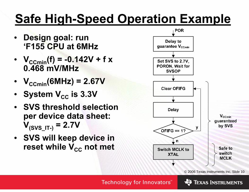
Safe High-Speed Operation Example• Design goal: run
‘F155 CPU at 6MHz• VCCmin(f) = -0.142V + f x
0.468 mV/MHz• VCCmin(6MHz) = 2.67V• System VCC is 3.3V• SVS threshold selection
per device data sheet: V(SVS_IT-) = 2.7V
• SVS will keep device in reset while VCC not met

© 2006 Texas Instruments Inc, Slide 11
Safe Flash ISP Example• Requirement:
VCC min = 2.7V during Flash ISP for ’F155
• System VCC is 3.3V• SVS threshold selection
per device data sheet: V(SVS_IT-) = 2.7V
• SVS will set SVSFG in case of low-voltage condition
• Enable/disable SVS to conserve power
Set SVS to 2.7V,Wait for SVSOP,
Clear SVSFG
n
y
Do Flash ISP
SVSFG == 1?
Flash ISP OK Flash ISP Error
Disable SVS
VCCguardedby SVS
© 2006 Texas Instruments Inc, Slide 12
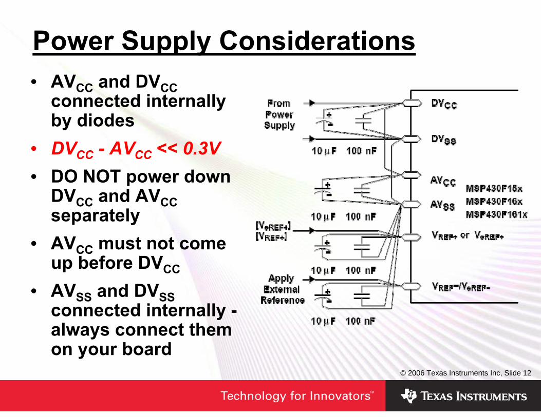
Power Supply Considerations• AVCC and DVCC
connected internallyby diodes
• DVCC - AVCC << 0.3V• DO NOT power down
DVCC and AVCCseparately
• AVCC must not comeup before DVCC
• AVSS and DVSSconnected internally -always connect them on your board

© 2006 Texas Instruments Inc, Slide 13
• Startup and Power Supply• ESD• Board Design• Crystal Considerations• Built-in Protection• Software Considerations
Agenda

© 2006 Texas Instruments Inc, Slide 14
ESD Considerations• MSP430s comply with
standard TI ESD specs:HBM = 1.5KVCDM = 500VMM = 200V
• System level spec –robust design is a must
• TI testing does not substitute robust system design

© 2006 Texas Instruments Inc, Slide 15
ESD Protection Design Ideas• Use proper MSP430 supply decoupling, with caps
placed closely• Interface ICs with high level of built-in ESD protection• Transient voltage suppressors (e.g.: SN75240)• External series-Rs on I/O lines• Additional clamping diodes• Keep traces short, lead length is critical because of
inductance:V = L x di / dtL for leads and PCB = 20nH / inchESD hits can induce di / dt of 10A / 500psV = 400 V/inch

© 2006 Texas Instruments Inc, Slide 16
No influence, ideal Direct discharge
Influence through holes
Direct discharge to cables
Secondary discharge from isolated metal
Plastic enclosure
ESD Effects Through Enclosures

© 2006 Texas Instruments Inc, Slide 17
Lens
Poor Better Poor Better
Enclosure Openings• No direct openings or keep PCB away from openings• Use gasket around LCD opening• LEDs are particularly vulnerable - direct path to PC
board

© 2006 Texas Instruments Inc, Slide 18
Poor Better Best
Enclosure Cables• Properly ground cables entering the enclosure• Added protection often required

© 2006 Texas Instruments Inc, Slide 19
ESD Device Protection• Series R most basic• Also helps reduce inductive Vcc ringing at power• Can combine series R with diodes for added
protection• Suppression devices such as varistors, thyristors,
TVS diodes, etc. should be used in extreme cases

© 2006 Texas Instruments Inc, Slide 20
• Startup and Power Supply• ESD• Board Design• Crystal Considerations• Built-in Protection• Software Considerations
Agenda

© 2006 Texas Instruments Inc, Slide 21
PCB Layout Fundamentals• Use ground plane where possible to lower current-
path inductance• Properly terminate unused MSP430 pins• No floating copper islands on PCB - they can induce
noise and arc in presence of ESD• Avoid crossing breaks in GND plane with traces as
this increases loop inductance and EMI radiation• Keep loop areas of switching signals as small as
possible• Keep loop area of the oscillator signals as small as
possible• Always keep forward and return currents together!

© 2006 Texas Instruments Inc, Slide 22
~I
I/2
I/2
~I
What Are Current Loops?• The distribution of the current going through two
possible paths is dependant on the inductance of those paths

© 2006 Texas Instruments Inc, Slide 23
~I
a)
b)
c)
~
Groundplane
cable
d)
Where Are Current Loops?• Examples for closed current loops as a radiation
source: Multi-layer PCB, Signal loop on a single layer PCB, Cable, Gnd loop closed by cables.

© 2006 Texas Instruments Inc, Slide 24
Signal
Return Current
Poor Better Best
Minimize Current Loops In Layout• Minimizing current loops minimizes inductive
coupling• Helps both EMI and ESD performance

© 2006 Texas Instruments Inc, Slide 25
How To Terminate Unused Pins?• I/O: Open, switched to port function, output direction• XIN: DVCC, XT2IN: DVSS
• XOUT, XT2OUT: Open• ADC VREF+: Open• ADC VeREF+, VREF-/VeREF-: DVSS
• R03: DVSS
• LCD signals COMx, Sxx: Open• JTAG signals TDO, TDI, TMS, TCK, Test: Open• RST/NMI: 47kΩ pullup + 10nF pulldown• See MSP430xxx Family User’s Guides
© 2006 Texas Instruments Inc, Slide 26
System Design Best Practices• Proper layout is important!• No direct enclosure openings or keep PCB away from
openings• Ground the connector shrouds• Ground the enclosure• Provide ESD a path to ground• Keep MSP430 out of path of ESD• Use gasket around LCD opening• LEDs are particularly vulnerable - direct path to PC
board (use light conductors or lenses)

© 2006 Texas Instruments Inc, Slide 27
• Startup and Power Supply• ESD• Board Design• Crystal Considerations• Built-in Protection• Software Considerations
Agenda

© 2006 Texas Instruments Inc, Slide 28
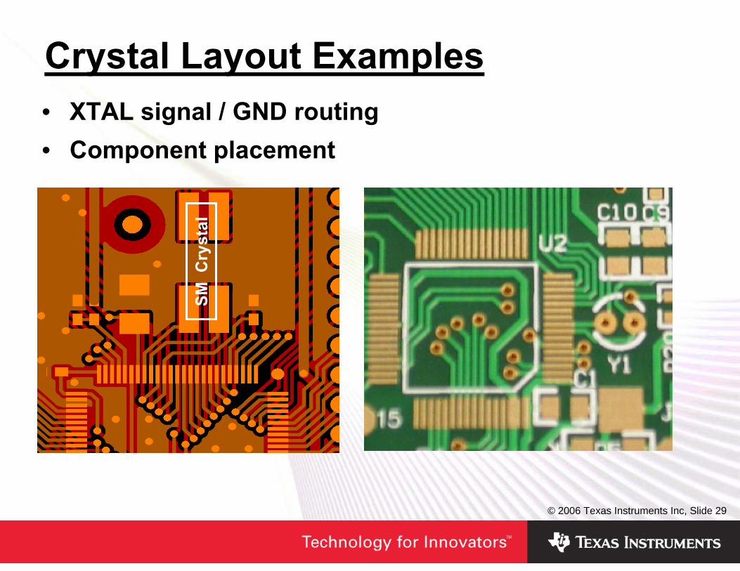
• Crystal as close the to MSP430 as possible• Short and direct traces, no traces underneath• Keep away switching signals• Ground crystal can, use guard ring around leads• Ground plane underneath crystal
Crystal Layout
© 2006 Texas Instruments Inc, Slide 29
Crystal Layout Examples
SM C
ryst
al
• XTAL signal / GND routing• Component placement

© 2006 Texas Instruments Inc, Slide 30
Crystal Layout Example - 28 Pin• Crystal as close as
possible at XIN/XOUT terminals
• GND below the crystal and load capacitors connected to the Vssterminal
• Load capacitors grounded closely to each other

© 2006 Texas Instruments Inc, Slide 31
Crystal Layout Examples - F41x• Same principles• Use the NC pins beside XIN/XOUT for GND ring
© 2006 Texas Instruments Inc, Slide 32
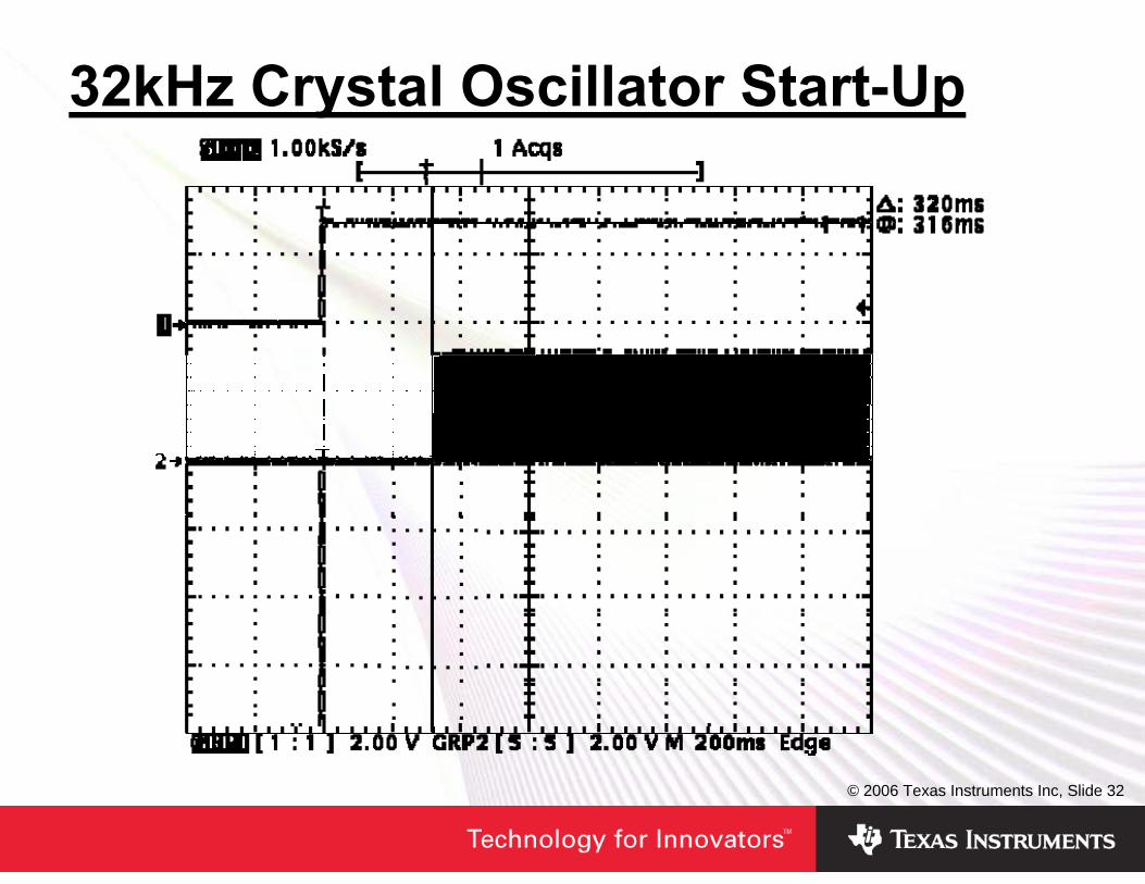
32kHz Crystal Oscillator Start-Up

© 2006 Texas Instruments Inc, Slide 33
• Switching signals near the crystal can cause dropout
Poor Layout Good Layout
Crystal Dropout

© 2006 Texas Instruments Inc, Slide 34
Poor Layout Good Layout
Crystal Oscillator Jitter• Poor design can cause jitter
© 2006 Texas Instruments Inc, Slide 35
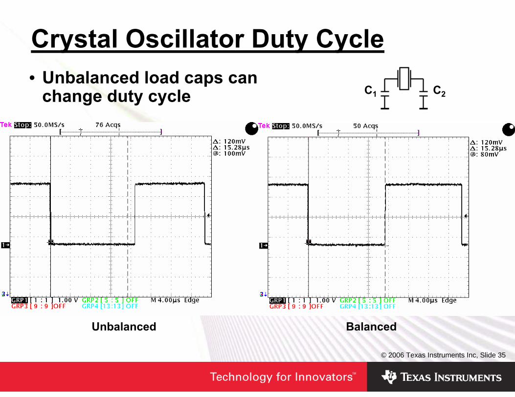
C1 C2
Unbalanced Balanced
Crystal Oscillator Duty Cycle• Unbalanced load caps can
change duty cycle

© 2006 Texas Instruments Inc, Slide 36
• Startup and Power Supply• ESD• Board Design• Crystal Considerations• Built-in Protection• Software Considerations
Agenda

© 2006 Texas Instruments Inc, Slide 37
XTAL Fault Detection Overview
N/AYESNOYES‘F1xx
YESYESXT2 ModeYESYESXT1 LF ModeYESYESXT1 HF Mode
YESN/AFLL
‘F4xx‘F2xx
LFXT1OF
XT2OFOFIFG
ACCVIFG
RST/NMI
NMIIFG
XT1OF
DCOF
What if…• FLL? Flash ISP?• RTC? WDT?• LPMx wakeup?

© 2006 Texas Instruments Inc, Slide 38
XTAL Failsafe Operation• XTAL Oscillator Faults are…
Set if respective OSC is turned on and failingSet on PORReset if oscillator functions normally again
• DCOF set when DCO is on min/max boundary (‘F4xx)• Individual Oscillator Faults will set OFIFG• OFIFG can generate NMI• OFIFG switches MCLK to DCO• OFIFG is latched on POR

© 2006 Texas Instruments Inc, Slide 39
NMI Handler Flow• De-mux as
shown• Re-enable with
very last ISRinstruction
• Use C-compilerintrinsic:_BIS_NMI_IE1(…)
• IFG must betruly clearbefore re-enabling
; Assembly Example
bis.b #OFIE,&IE1reti
; Assembly Example
bis.b #OFIE,&IE1reti

© 2006 Texas Instruments Inc, Slide 40
XTAL Fault - Limp Mode Ideas• How to maintain basic functionality?• Constraints:
Available clock sourcesSystem requirements
• ‘F1xx / ‘F2xx / ‘F4xx: Use DCO instead of HF-XTAL• ‘F2xx: Use VLOCLK instead of LF-XTAL• ‘F4xx: If LF-XTAL fails, disable FLL
(SCG0 = 1) & control DCO manually. If LCD is used, A/C waveforms can be generated by manipulating BTCNT1 directly.
• Periodically clear, wait, & re-check OFIFG• Use original clock-setup once OFIFG stays clear

© 2006 Texas Instruments Inc, Slide 41
Minimum Pulse Clock Filter• All ’F2xx devices• On all clock input(s)• Prevents high-frequency
components > max ratings from entering clock tree
• Glitches & high-frequency pulses can cause erroneous instruction fetching
• Always-on• Increases system
robustness

© 2006 Texas Instruments Inc, Slide 42
Watchdog Timer+ Clock Source
• All ‘F2xx devices and ‘F(E)42x(x)• Active clock source can’t be disabled (WDT mode)• May affect LPMx behavior & current consumption• WDT(+) always powers up active on ALL MSP430’s

© 2006 Texas Instruments Inc, Slide 43
WDT+ Failsafe Operation• If ACLK / SMCLK fail,
clock source = MCLK(WDT+ fail safe feature)
• If MCLK is sourced from a crystal, and the crystal has failed,MCLK = DCO(XTAL fail safe feature) Fail-Safe
Logic
16-bitCounter
A EN
SMCLK
ACLK
MCLK
1
1
CLK
WDTSSEL WDTHOLD

© 2006 Texas Instruments Inc, Slide 44
PC Range Monitoring• Additional protection against software errors• On all MSP430F2xx devices, MSP430F(E)42x(x)• An instruction fetch from the peripheral address
range 0x0000 − 0x01FF resets the device#include <msp430x42x0.h>
void main(void)P1DIR |= 0x01; // Set P1.0 to output directionfor (;;) volatile unsigned int i = 50000;P1OUT ^= 0x01; // Toggle P1.0 using XORdo i--; while (i != 0); // Delay((void (*)())0x170)(); // Invalid fetch causes POR
// ("call #0170h")
#include <msp430x42x0.h>
void main(void)P1DIR |= 0x01; // Set P1.0 to output directionfor (;;) volatile unsigned int i = 50000;P1OUT ^= 0x01; // Toggle P1.0 using XORdo i--; while (i != 0); // Delay((void (*)())0x170)(); // Invalid fetch causes POR
// ("call #0170h")
© 2006 Texas Instruments Inc, Slide 45
• Startup and Power Supply• ESD• Board Design• Crystal Considerations• Built-in Protection• Software Considerations
Agenda

© 2006 Texas Instruments Inc, Slide 46
Software Considerations – Flash• Simple Flash Write Routine• Improvements
Variable generated keysAddress range checkingSVS usage during flash writeDestruction of variable keys before exitWriting checksum of data
© 2006 Texas Instruments Inc, Slide 47
Software considerations - Startup• Checksum of all program code is stored in flash• On startup, code calculates a checksum against all
program code, compares this to saved value• Only ‘known good’ code gets executed.• Can be accomplished as a Vcc rise / Crystal delay.

IMPORTANT NOTICE
Texas Instruments Incorporated and its subsidiaries (TI) reserve the right to make corrections, modifications, enhancements,improvements, and other changes to its products and services at any time and to discontinue any product or service without notice.Customers should obtain the latest relevant information before placing orders and should verify that such information is current andcomplete. All products are sold subject to TI’s terms and conditions of sale supplied at the time of order acknowledgment.
TI warrants performance of its hardware products to the specifications applicable at the time of sale in accordance with TI’sstandard warranty. Testing and other quality control techniques are used to the extent TI deems necessary to support thiswarranty. Except where mandated by government requirements, testing of all parameters of each product is not necessarilyperformed.
TI assumes no liability for applications assistance or customer product design. Customers are responsible for their products andapplications using TI components. To minimize the risks associated with customer products and applications, customers shouldprovide adequate design and operating safeguards.
TI does not warrant or represent that any license, either express or implied, is granted under any TI patent right, copyright, maskwork right, or other TI intellectual property right relating to any combination, machine, or process in which TI products or servicesare used. Information published by TI regarding third-party products or services does not constitute a license from TI to use suchproducts or services or a warranty or endorsement thereof. Use of such information may require a license from a third party underthe patents or other intellectual property of the third party, or a license from TI under the patents or other intellectual property of TI.
Reproduction of information in TI data books or data sheets is permissible only if reproduction is without alteration and isaccompanied by all associated warranties, conditions, limitations, and notices. Reproduction of this information with alteration is anunfair and deceptive business practice. TI is not responsible or liable for such altered documentation.
Resale of TI products or services with statements different from or beyond the parameters stated by TI for that product or servicevoids all express and any implied warranties for the associated TI product or service and is an unfair and deceptive businesspractice. TI is not responsible or liable for any such statements.
TI products are not authorized for use in safety-critical applications (such as life support) where a failure of the TI product wouldreasonably be expected to cause severe personal injury or death, unless officers of the parties have executed an agreementspecifically governing such use. Buyers represent that they have all necessary expertise in the safety and regulatory ramificationsof their applications, and acknowledge and agree that they are solely responsible for all legal, regulatory and safety-relatedrequirements concerning their products and any use of TI products in such safety-critical applications, notwithstanding anyapplications-related information or support that may be provided by TI. Further, Buyers must fully indemnify TI and itsrepresentatives against any damages arising out of the use of TI products in such safety-critical applications.
TI products are neither designed nor intended for use in military/aerospace applications or environments unless the TI products arespecifically designated by TI as military-grade or "enhanced plastic." Only products designated by TI as military-grade meet militaryspecifications. Buyers acknowledge and agree that any such use of TI products which TI has not designated as military-grade issolely at the Buyer's risk, and that they are solely responsible for compliance with all legal and regulatory requirements inconnection with such use.
TI products are neither designed nor intended for use in automotive applications or environments unless the specific TI productsare designated by TI as compliant with ISO/TS 16949 requirements. Buyers acknowledge and agree that, if they use anynon-designated products in automotive applications, TI will not be responsible for any failure to meet such requirements.
Following are URLs where you can obtain information on other Texas Instruments products and application solutions:
Products Applications
Amplifiers amplifier.ti.com Audio www.ti.com/audio
Data Converters dataconverter.ti.com Automotive www.ti.com/automotive
DSP dsp.ti.com Broadband www.ti.com/broadband
Interface interface.ti.com Digital Control www.ti.com/digitalcontrol
Logic logic.ti.com Military www.ti.com/military
Power Mgmt power.ti.com Optical Networking www.ti.com/opticalnetwork
Microcontrollers microcontroller.ti.com Security www.ti.com/security
RFID www.ti-rfid.com Telephony www.ti.com/telephony
Low Power www.ti.com/lpw Video & Imaging www.ti.com/videoWireless
Wireless www.ti.com/wireless
Mailing Address: Texas Instruments, Post Office Box 655303, Dallas, Texas 75265Copyright © 2007, Texas Instruments Incorporated


![[MSP430] GPIO](https://img.dokumen.tips/doc/110x75/55cf9df0550346d033aff200/msp430-gpio.jpg)