Embed Size (px)
Citation preview

Application Report SLAA089C – February 2006
1
Features of the MSP430 Bootstrap Loader Stefan Schauer MSP430
ABSTRACT
The MSP430 bootstrap loader (BSL) enables users to communicate with embedded memory in the MSP430 microcontroller during the prototyping phase, final production, and in service. Both the programmable memory (flash memory) and the data memory (RAM) can be modified as required.
The commonly used UART protocol with RS232 interfacing is supported, allowing flexible use of both hardware and software.
To use the bootstrap loader, a specific BSL entry sequence has to be applied to specific device pins. An added sequence of commands initiates the desired function. A boot loading session can be exited by continuing operation at a defined user program address, or by the reset condition.
Access to the MSP430 memory via the bootstrap loader is protected against misuse by a user-defined password.
Contents 1 Introduction .....................................................................................................................................3 2 Standard RESET and BSL Entry Sequence..................................................................................3
2.1 MSP430 20- and 28-Pin Flash Devices With Shared JTAG Pins..............................................3 2.2 MSP430 Flash Devices With Dedicated JTAG Pins .................................................................4
3 UART Protocol.................................................................................................................................5 4 Synchronization Sequence ............................................................................................................5 5 Commands.......................................................................................................................................6
5.1 Unprotected Commands ...........................................................................................................6 5.2 Password Protected Commands...............................................................................................6
6 Programming Flow..........................................................................................................................6 7 Data Frame.......................................................................................................................................7
7.1 Data Stream Structure...............................................................................................................7 7.2 Checksum .................................................................................................................................8 7.3 Example Sequence ...................................................................................................................8 7.4 Commands - Detailed Description.............................................................................................9 7.4.1 General ..........................................................................................................................9 7.4.2 RX Data Block ...............................................................................................................9 7.4.3 RX Password...............................................................................................................10 7.4.4 Mass Erase..................................................................................................................10 7.4.5 Erase Segment............................................................................................................10 7.4.6 Erase Check ................................................................................................................11 7.4.7 Change Baud Rate ......................................................................................................12 7.4.8 Load PC.......................................................................................................................13 7.4.9 TX Data Block..............................................................................................................14 7.4.10 TX BSL Version ...........................................................................................................14

SLAA089C
2 Features of the MSP430 Bootstrap Loader
8 Loadable BSL ................................................................................................................................15 9 Exiting the BSL..............................................................................................................................16 10 Password Protection.....................................................................................................................16 11 Code Protection Fuse ...................................................................................................................17 12 BSL Internal Settings and Resources .........................................................................................17
12.1 Chip Identification and BSL Version........................................................................................17 12.2 Vectors to Call the BSL Externally...........................................................................................17 12.3 Initialization Status ..................................................................................................................18 12.4 Memory Allocation and Resources..........................................................................................19
13 Special Consideration for BSL Version 1.10 ..............................................................................20 14 References.....................................................................................................................................20 Appendix A Differences Between Devices and BSL Versions..................................................21
Appendix B MSP430 BSL Replicator...........................................................................................26 B.1 BSL Replicator Overview..........................................................................................................26
B.2 Implementation .........................................................................................................................27 B.3 BSL Message Functions ...........................................................................................................29 B.4 BSL Implementation Functions .................................................................................................31 B.5 Building a Downloadable MSP430 Application .........................................................................32
Figures Figure 1. Standard RESET Sequence....................................................................................................3 Figure 2. BSL Entry Sequence at Shared JTAG Pins...........................................................................4 Figure 3. BSL Entry Sequence at Dedicated JTAG Pins......................................................................4 Figure 4. BSL Replicator Block Diagram.............................................................................................26 Figure 5. BSL Replicator Flow Chart ...................................................................................................28 Figure 6. BSL Replicator Flow Chart Con’t. ........................................................................................29
Tables Table 1. Data Frame of BSL Commands..............................................................................................7 Table 2. Recommendations for MSP430F149....................................................................................13 Table 3. Recommendations for MSP430F2131..................................................................................13 Table 4. BSL Version 1.10 on F13x, F14x(1), F11x, and F11x1 ........................................................21 Table 5. BSL Version 1.30 on F41x, F11x, and F11x1.......................................................................22 Table 6. BSL Version 1.40 on F12x.....................................................................................................23 Table 7. BSL Version 1.60 on F11x2, F12x2, F43x/44x, FE42x, FW42x, FG43x, F415/417, F42x0.24 Table 8. BSL Version 2.01 on F21x1...................................................................................................25
SLAA089C
Features of the MSP430 Bootstrap Loader 3
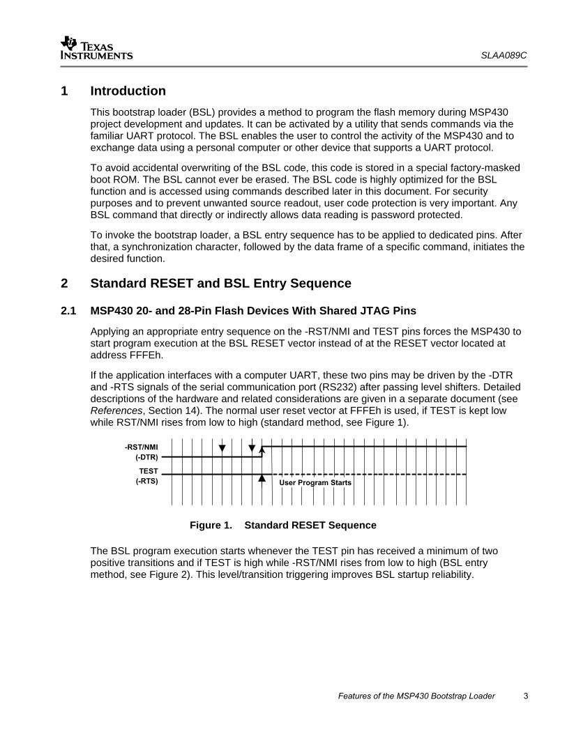
1 Introduction This bootstrap loader (BSL) provides a method to program the flash memory during MSP430 project development and updates. It can be activated by a utility that sends commands via the familiar UART protocol. The BSL enables the user to control the activity of the MSP430 and to exchange data using a personal computer or other device that supports a UART protocol.
To avoid accidental overwriting of the BSL code, this code is stored in a special factory-masked boot ROM. The BSL cannot ever be erased. The BSL code is highly optimized for the BSL function and is accessed using commands described later in this document. For security purposes and to prevent unwanted source readout, user code protection is very important. Any BSL command that directly or indirectly allows data reading is password protected.
To invoke the bootstrap loader, a BSL entry sequence has to be applied to dedicated pins. After that, a synchronization character, followed by the data frame of a specific command, initiates the desired function.
2 Standard RESET and BSL Entry Sequence
2.1 MSP430 20- and 28-Pin Flash Devices With Shared JTAG Pins
Applying an appropriate entry sequence on the -RST/NMI and TEST pins forces the MSP430 to start program execution at the BSL RESET vector instead of at the RESET vector located at address FFFEh.
If the application interfaces with a computer UART, these two pins may be driven by the -DTR and -RTS signals of the serial communication port (RS232) after passing level shifters. Detailed descriptions of the hardware and related considerations are given in a separate document (see References, Section 14). The normal user reset vector at FFFEh is used, if TEST is kept low while RST/NMI rises from low to high (standard method, see Figure 1).
-RST/NMI(-DTR)
TEST(-RTS) User Program Starts
Figure 1. Standard RESET Sequence
The BSL program execution starts whenever the TEST pin has received a minimum of two positive transitions and if TEST is high while -RST/NMI rises from low to high (BSL entry method, see Figure 2). This level/transition triggering improves BSL startup reliability.
SLAA089C
4 Features of the MSP430 Bootstrap Loader
-RST/NMI(-DTR)
TEST(-RTS)
Bootstrap Loader Starts
Figure 2. BSL Entry Sequence at Shared JTAG Pins
The TEST signal is normally used simply to switch the port pins P1.7 – P1.4 between their application function and the JTAG function. If the second rising edge at the TEST pin is applied while -RST/NMI is still low, the TEST signal is kept low internally (application mode).
The BSL will not be started (via the BSL RESET vector), if:
• There are less than two positive edges at the TEST pin while -RST/NMI is low
• TEST is low when -RST/NMI rises from low to high
• JTAG has control over the MSP430 resources
• Supply voltage VCC drops down and a power-on reset (POR) is executed
• RST/NMI pin is configured for NMI functionality (NMI bit is set)
NOTE: The minimum timing for this sequence has to be within the limits specified for the corresponding pin in the datasheet.
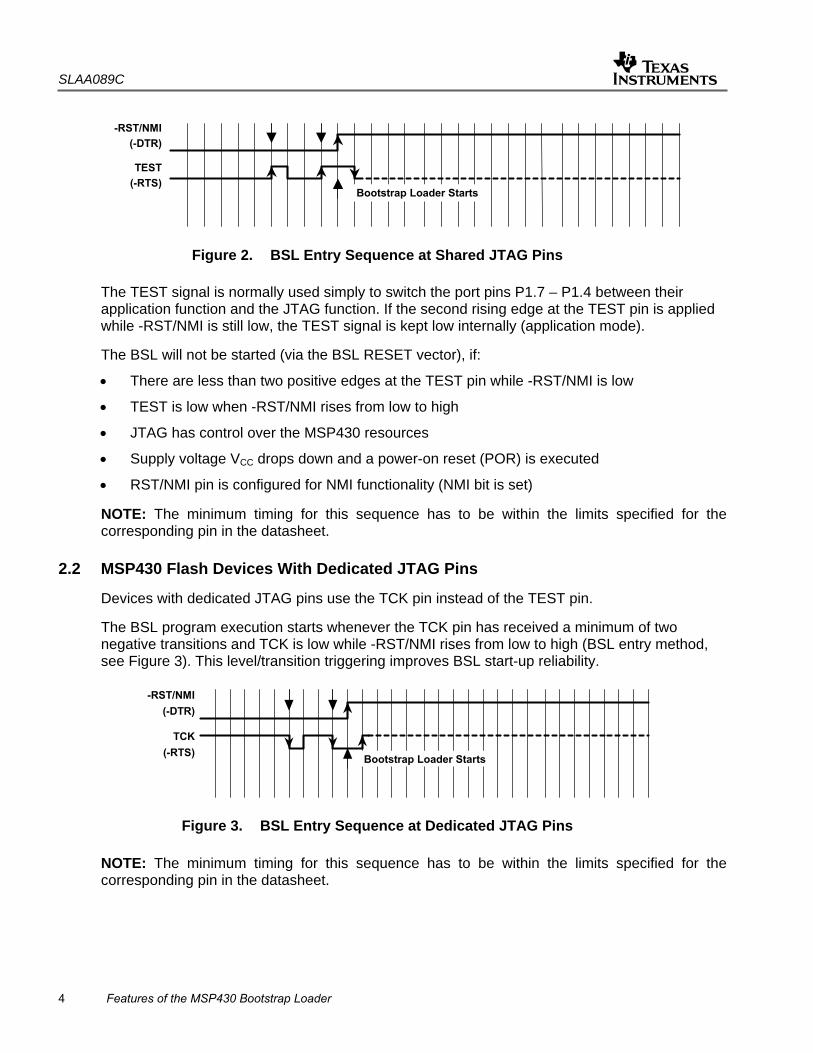
2.2 MSP430 Flash Devices With Dedicated JTAG Pins
Devices with dedicated JTAG pins use the TCK pin instead of the TEST pin.
The BSL program execution starts whenever the TCK pin has received a minimum of two negative transitions and TCK is low while -RST/NMI rises from low to high (BSL entry method, see Figure 3). This level/transition triggering improves BSL start-up reliability.
-RST/NMI(-DTR)
TCK(-RTS) Bootstrap Loader Starts
Figure 3. BSL Entry Sequence at Dedicated JTAG Pins
NOTE: The minimum timing for this sequence has to be within the limits specified for the corresponding pin in the datasheet.

SLAA089C
Features of the MSP430 Bootstrap Loader 5
The BSL will not be started (via the BSL RESET vector), if:
• There are less than two negative edges at TCK pin while -RST/NMI is low
• TCK is high if -RST/NMI rises from low to high
• JTAG has control over the MSP430 resources
• Supply voltage VCC drops down and a power on reset (POR) is executed
• RST/NMI pin is configured for NMI functionality (NMI bit is set)
3 UART Protocol The UART protocol applied here is defined as: • Baud rate is fixed to 9600 baud in half duplex mode (one sender at a time). • Start bit, 8 data bits (LSB first), an even parity bit, 1 stop bit. • Handshake is performed by an acknowledge character. • Minimum time delay before sending new characters after characters have been received
from the MSP430 BSL: 1.2ms
NOTE: Applying baud rates other than 9600 baud at initialization results in communication problems or violates the flash memory write timing specification. The flash memory may be extensively stressed or may react with unreliable program/erase operations.
4 Synchronization Sequence Before sending any command to the BSL, a synchronization character (SYNC) with its value of 80h has to be sent to the BSL. This character is necessary to calculate all the essential internal parameters, which maintain UART and flash memory program/erase timings. It provides the BSL system time reference. Once this is received, an acknowledge DATA_ACK = 90h is sent back by the BSL to confirm successful reception.
This sequence has to be done before every command which is sent to the BSL.
NOTE: The synchronization character is not part of the Data Frame described later.
SLAA089C
6 Features of the MSP430 Bootstrap Loader
5 Commands Two categories of commands are available: commands needing a password and commands that do not require a password. The password protection safeguards every command that potentially allows direct or indirect data access.
5.1 Unprotected Commands
• Receive password
• Mass erase (erase entire flash memory, main- as well as information-memory)
• Transmit BSL version (V1.60 or higher or in loadable BL_150S_14x.txt)
• Change baud rate (V1.60 or V1.61 or in loadable BL_150S_14x.txt)
5.2 Password Protected Commands
• Receive data block to program flash memory, RAM, or peripherals
• Transmit data block
• Erase segment
• Erase check (V1.60 or higher or in loadable BL_150S_14x.txt)
• Load program counter and start user program
• Change baud rate (moved to a protected command starting with BSL version 2.01)
6 Programming Flow The write access (RX data block command) to the flash memory/RAM or peripheral modules area is executed online. That means a data byte/word is processed immediately after receipt and the write cycle is finished before a following byte/word has completely arrived. Therefore, the entire write time is determined by the baud rate and no buffering mechanism is necessary.
Data sections located below the flash memory area address are assumed to be loaded into the RAM or peripheral module area, and thus no specific flash control bits are affected.
NOTE: When losing control over the UART protocol either by line faults or by violating the data frame conventions, the only way to recover is to rerun the BSL entry sequence to initiate another BSL session.
SLAA089C
Features of the MSP430 Bootstrap Loader 7
7 Data Frame To get high data security during the data transmission a data frame protocol is used which is called serial standard protocol (SSP). The BSL is considered the receiver in Table1.
For more information on serial standard protocol (SSP), see Application of Bootstrap Loader in MSP430 With Flash Hardware and Software Proposal (SLAA096).
7.1 Data Stream Structure
• The first 8 bytes (HDR through LH) are mandatory (xx represents dummy data).
• Data bytes D1 to Dn are optional.
• Two bytes (CKL and CKH) for checksum are mandatory.
• Acknowledge done by the BSL is mandatory except with the TX data block and TX BSL version commands.
Table 1. Data Frame of BSL Commands
Received BSL
Command
H D R
C M D
L1
L2
AL
AH
LL
LH
D1
D2 … Dn
C K L
C K H
A C K
RX data block 80 12 n n AL AH n–4 0 D1 D2 … Dn–4 CKL CKH ACK
RX password 80 10 24 24 xx xx xx xx D1 D2 … D20 CKL CKH ACK
Erase segment 80 16 04 04 AL AH 02 A5 — — — — CKL CKH ACK
Erase main or info
80 16 04 04 AL AH 04 A5 — — — — CKL CKH ACK
Mass erase 80 18 04 04 xx xx xx xx — — — — CKL CKH ACK
Erase check 80 1C 04 04 AL AH LL LH — — — — CKL CKH ACK
Change baud rate
80 20 04 04 D1 D2 D3 xx — — — — CKL CKH ACK
Load PC 80 1A 04 04 AL AH xx xx — — — — CKL CKH ACK
TX data block 80 14 04 04 AL AH n 0 — — — — CKL CKH —
BSL responds 80 xx n n D1 D2… … … ... … Dn CKL CKH —
TX BSL version 80 1E 04 04 xx xx xx xx — — — — CKL CKH —
BSL responds 80 xx 10 10 D1 D2… … … … … D10 CKL CKH — Notes: All numbers are bytes in hexadecimal notation. ACK is sent back by the BSL. The synchronization sequence is not part of the data frame. The erase check and TX BSL version commands are not members of the standard command set (V1.50 or higher). The change baud rate command is not a member of the standard command set (V1.60 or higher or in loadable BL_150S_14x.txt).
Abbreviations:
HDR Header: Any value between 80h and 8Fh (normally 80h).
CMD Command identification
L1, L2 Number of bytes consisting of AL through Dn Restrictions: L1 = L2, L1 < 255, L1 even.
SLAA089C
8 Features of the MSP430 Bootstrap Loader
AL, AH Block start address or erase (check) address or jump address LO/HI byte
LL, LH Number of pure data bytes (max. 250) or erase information LO/HI byte or block length of erase check (max. FFFFh)
D1 … Dn Data bytes
CKL, CKH 16-bit checksum LO/HI byte
xx Can be any data
-- No character (data byte) received/transmitted
ACK The acknowledge character returned by the BSL, can be either DATA_ACK = 90h: Frame was received correctly, command was executed successfully, or DATA_NAK = A0h: Frame not valid (e.g., wrong checksum, L1 ≠ L2), command is not defined, is not allowed, or was executed unsuccessfully.
n Number of bytes consisting of AL through Dn
7.2 Checksum
The 16-bit (2 bytes) checksum is calculated over all received/transmitted bytes B1 … Bn in the data frame except the checksum bytes themselves by XORing words (2 successive bytes) and inverting the result.
This means that B1 is always the HDR byte and Bn is the last data byte just before the CKL byte.
Formula:
CHECKSUM = INV [ (B1 + 256*B2) XOR (B3 + 256*B4) XOR … XOR (Bn–1 + 256*Bn) ]
or
CKL = INV [ B1 XOR B3 XOR … XOR Bn–1 ] ; CKH = INV [ B2 XOR B4 XOR … XOR Bn ]
7.3 Example Sequence
The following example shows a request to read the Memory of the MSP430 from location 0x0F00:
• TO BSL : 80 (Sych character sent to the BSL)
• FROM BSL : 90 (Acknowledge from BSL)
• TO BSL : 80 14 04 04 F0 0F 0E 00 85 E0 (Send Command to read memory from 0x0F00, len 0x000E)
• FROM BSL : 80 00 0E 0E F2 13 40 40 00 00 00 00 00 00 02 01 01 01 C0 A2 (Returned values from BSL)
SLAA089C
Features of the MSP430 Bootstrap Loader 9
7.4 Commands - Detailed Description
See Table 1.
7.4.1 General
Besides the header byte HDR (80h) and the command identification CMD, the frame length bytes L1 and L2 (which must be equal) hold the number of bytes following L2, excluding the checksum bytes CKL and CKH.
Bytes AL, AH, LL, LH, D1…Dn are command-specific. However, the checksum bytes CKL (low byte) and CKH (high byte) are mandatory.
If the data frame has been received correctly and the command execution was successful, an acknowledge character DATA_ACK = 90h is sent back by the BSL. Incorrectly received data frames, unsuccessful operations, commands which are locked or not defined are confirmed with a DATA_NAK = A0h.
NOTE: BSL versions lower than V1.30 support only byte access operations. The peripheral module addresses at 0100h–01FFh thus cannot be accessed correctly because they are word-oriented. From version V1.30 and up, addresses 0000h–00FFh are accessed in byte mode; all others are accessed in word mode.
7.4.2 RX Data Block
The receive data block command is used for any write access to the flash memory/RAM or peripheral module control registers at 0000h–01FFh. It is password protected.
The 16-bit even-numbered block start address is defined in AL (low byte) and AH (high byte). The 16-bit even-numbered block length is defined in LL (low byte) and LH (high byte). Because pure data bytes are limited to a maximum of 250, LH is always 0.
The following data bytes are succeeded by the checksum bytes CKL (low byte) and CKH (high byte). If the receipt and programming of the appropriate data block was successful, an acknowledge character DATA_ACK is sent back by the BSL. Otherwise, the BSL confirms with a DATA_NAK.
NOTE: BSL versions V1.40 and higher support online verification inside the MSP430 for addresses 0200h–FFFFh which reduces programming/verification time to 50 percent. Online verification means that the data is immediately verified with the data which is written into the flash without transmitting it again. In case of an error the loadable bootstrap loader BL_150S_14x.txt additionally store the first incorrectly written location address+3 into the error address buffer in the RAM at address 0200h (021Eh for F14x devices).
SLAA089C
10 Features of the MSP430 Bootstrap Loader
7.4.3 RX Password
The receive password command is used to unlock the password-protected commands, which perform reading, writing, or segment-erasing memory access. It is not password protected.
Neither start address nor block length information is necessary because the 32-byte password is always located at addresses FFE0h–FFFFh. Data bytes D1 to D20h hold the password information starting with D1 at address FFE0h.
If the receipt and verification of the password is correct a positive acknowledge DATA_ACK is sent back by the BSL and the password-protected commands become unlocked. Otherwise the BSL confirms with a DATA_NAK.
Once the protected commands become unlocked they remain unlocked until another BSL entry is initiated.
7.4.4 Mass Erase
The mass erase command erases the entire flash memory area (main memory plus information memory, see corresponding data sheet). It is not password protected.
All parameters shown in Table 1 are mandatory. After erasing, an acknowledge character DATA_ACK is sent back by the BSL.
Mass erase initializes the password area to 32 times 0FFh.
NOTE: BSL versions V2.01 and higher support automatic clearing of the LOCKA bit protecting Information Flash memory. When the BSL is entered from a rest condition, LOCKA will be cleared by the BSL in order to mass erase the Flash including information memory. When the BSL is entered in-application, user software should take care that LOCKA = 1 prior to initiating the BSL. Otherwise information Flash will not be erased during a BSL mass erase.
7.4.5 Erase Segment
The erase segment command erases specific flash memory segments. It is password protected.
The address bytes AL (low byte) and AH (high byte) select the appropriate segment. Any even-numbered address within the segment to be erased is valid. After segment erasing, an acknowledge character DATA_ACK is sent back by the BSL (V1.40 or lower).
BSL versions V1.60 or higher perform a subsequent erase check of the corresponding segment and respond with a DATA_NAK if the erasure was not successful. In this case the first unerased location address+1 is stored in the error address buffer in the RAM at address 0200h (021Eh for F14x devices). In this version a problem occurs if only one of the info memory segments is erased. In this case an error will be reported because an automatic erase check over the whole info memory is performed. As a solution either erase the whole info memory or do a separate erase check after the erase - even if the erase reported an error.
Erase segment 0 clears the password area, and therefore the remaining password is 32 times 0FFh.

SLAA089C
Features of the MSP430 Bootstrap Loader 11
When applying LL = 0x04 and LH = 0xA5 a mass erasure of only the main memory is performed. Indeed this command has to be executed min. 12 times to achieve a total erasure time of >200ms. No subsequent erase check of the entire main memory is done. Use the erase check command additionally. Check the device datasheet for more information on the cumulative (mass) erase time which must be met and the number of erase cycles required.
The MSP430F1xxx and MSP430F4xxx device segmentation is configured as follows:
0FE00h–0FFFFh : Segment 0 Main memory 0FC00h–0FDFFh : Segment 1 0FA00h–0FBFFh : Segment 2 0F800h–0F9FFh : Segment 3 … … 01200h–013FFh : Segment n-1 01100h–011FFh : Segment n 01080h–010FFh : Segment A Information memory 01000h–0107Fh : Segment B
The MSP430F2xxx device segmentation is configured as follows:
0FE00h–0FFFFh : Segment 0 Main memory 0FC00h–0FDFFh : Segment 1 0FA00h–0FBFFh : Segment 2 0F800h–0F9FFh : Segment 3 … … 01200h–013FFh : Segment n-1 01100h–011FFh : Segment n 01080h–010FFh : Segment A Information memory 01000h–0107Fh : Segment B
7.4.6 Erase Check
The erase check command verifies the erasure of flash memory within a certain address range. It is password protected.
The 16-bit block start address is defined in AL (low byte) and AH (high byte). The 16-bit block length is defined in LL (low byte) and LH (high byte). Both can be either even or odd numbered to allow odd boundary checking.
If the erase check of the appropriate data block was successful (all bytes contain 0FFh), an acknowledge character DATA_ACK is sent back by the BSL. Otherwise the BSL confirms with a DATA_NAK and the first not erased location address+1 is stored in the error address buffer at address 0200h (021Eh for F14x devices).
NOTE: This command is not a member of the standard command set. It is implemented in BSL version V1.60 and higher or in the loadable bootstrap loader BL_150S_14x.txt.

SLAA089C
12 Features of the MSP430 Bootstrap Loader
7.4.7 Change Baud Rate
The change baud rate command offers the capability of transmissions at higher baud rates than the default 9600 baud. With faster data transition shorter programming cycles can be achieved which is especially important with large flash memory devices. This command is not password protected.
Three control bytes D1 to D3 determine the selected baud rate. D1 and D2 set the processor frequency (f ≥ fmin), D3 indirectly sets the flash timing generator frequency (fFTGmin ≤ fFTG ≤ fFTGmax). In detail:
D1: F1xx: Basic clock module control register DCOCTL (DCO.2 … DCO.0) F2xx: Basic clock module control register DCOCTL (DCO.2 … DCO.0) F4xx: FLL+ system clock control register SCFI0 (D, FN_8 … FN_2)
D2: F1xx: basic clock module control register BCSCTL1 (XT2Off, Rsel.2 … Rsel.0) F2xx: basic clock module control register BCSCTL1 (XT2Off, Rsel.2 … Rsel.0) F4xx: FLL+ system clock control register SCFI1 (NDCO)
D3: 0: 9600 Baud 1: 19200 Baud 2: 38400 Baud
After receiving the data frame an acknowledge character DATA_ACK is sent back and the BSL becomes prepared for the selected baud rate. It is recommended for the BSL communication program to wait approximately 10 ms between baud rate alteration and succeeding data transmission to give the BSL clock system time for stabilization.
NOTE: The highest achievable baud rate depends on various system and environment parameters like supply voltage, temperature range, and minimum/maximum processor frequency. See the corresponding device specification / data sheet.
NOTE: This command is implemented on BSL versions V1.60 or higher or available in the loadable bootstrap loader BL_150S_14x.txt.

SLAA089C
Features of the MSP430 Bootstrap Loader 13
Table 2. Recommendations for MSP430F149 [F449] (TA = 25°C, VCC = 3.0 V, fmax = 6.7 MHz) (see Note 2)
Baud Rate (Baud)
Proc. Freq. fmin (MHz)
(see Note 4)
D1 DCOCTL [SCFI0]
(see Note 1)
D2 BCSCTL1 [SCFI1]
(see Note 1)
D3 (see Note 1)
Progr. / Verify60 Kbytes
(sec) (see Note 3)
9600 (init) 1.05 0x80 [00] 0x85 [98] 00 [00] 78 + 3.7 [0.0]
19200 2.1 0xE0 [00] 0x86 [B0] 01 [01] 39 + 3.7 [2.4]
38400 4.2 0xE0 [00] 0x87 [C8] 02 [02] 20 + 3.7 [2.4]
Table 3. Recommendations for MSP430F2131 (TA = 25°C, VCC = 3.0 V, fmax = 6.7 MHz) (see Note 2)
Baud Rate (Baud)
Proc. Freq. fmin (MHz)
(see Note 4)
D1 DCOCTL
(see Note 1)
D2 BCSCTL1
(see Note 1)
D3 (see Note 1)
Progr. / Verify60 Kbytes
(sec)
9600 (init) 1.05 0x80 0x88 00 78
19200 2.1 0x00 0x8B 01 39
38400 4.2 0x80 0x8C 02 20 Notes: 1. D1 to D3 are bytes in hexadecimal notation.
2. Values in brackets [ ] are related to MSP430F449. 3. Additional 3.7 [2.4] seconds result from loading, verifying, and launching the loadable BSL. 4. The minimum processor frequency is lower than in the standard ROM BSL (see Initialization Status, Section 12.3).
7.4.8 Load PC
The load program counter command directs the program counter (register R0) to any location within the entire address range. It is password protected.
After receiving the data frame an acknowledge character DATA_ACK is sent back by the BSL. Then the selected address is moved into the program counter. The program flow continues operation there, and the BSL session is terminated.
Be aware that the password protection is not active at this time.

SLAA089C
14 Features of the MSP430 Bootstrap Loader
7.4.9 TX Data Block
The transmit data block command is used for any read access to the flash memory/RAM or peripheral module control registers at 0000h–01FFh. It is password protected.
The 16-bit block start address is defined in AL (low byte) and AH (high byte). The 16-bit block length is defined in LL (low byte) and LH (high byte). Because pure data bytes are limited to a maximum of 250, LH is always 0. The checksum bytes CKL (low byte) and CKH (high byte) immediately follow this information.
Now the BSL responds with the requested data block. After transmitting HDR, dummy CMD, L1 and L2, The BSL sends data bytes D1 through Dn, followed by the checksum bytes CKL (low byte) and CKH (high byte). No acknowledge character is necessary.
7.4.10 TX BSL Version
The transmit BSL version command gives the user information about chip identification and bootstrap loader software version. It is not password protected.
The values for AL, AH, LL, and LH can be any data, but must be transmitted to meet the protocol requirements. The checksum bytes CKL (low byte) and CKH (high byte) immediately follow this information.
After that, the BSL responds with a 16-byte data block. After transmitting HDR, dummy CMD, L1 and L2, the BSL sends data bytes D1 through D16 (decimal), followed by the checksum bytes CKL (low byte) and CKH (high byte). No acknowledge character is necessary.
D1, D2 and D11, D12 (decimal) hold the specific information:
D1: Device family type (high byte) D2: Device family type (low byte) D11: BSL version (high byte) D12: BSL version (low byte)
The remaining 12 bytes are for internal use only.

SLAA089C
Features of the MSP430 Bootstrap Loader 15
8 Loadable BSL For upgrading the BSL functionality, sometimes it is suitable to load a higher version of BSL into the RAM of a device and apply the latest innovations. To do so, use the following BSL commands:
• RX password (unlock password protection for following commands)
• RX data block (code of loadable BSL, code section address ≥ 220h)
• TX data block (for verification)
• RX data block (get start address from first code section address)
• Load program counter PC (with start address of loadable BSL)
• Wait at least 5ms till the new loaded BSL has executed the initialized routine
• RX password (unlock password protection for loaded BSL)
• Perform any command (with loaded BSL)
The following loadable BSLs are available:
• BL_150S_14x.txt is a complete BSL for the F14x/F13x family with BSL version 1.10. All features of BSL version V1.60 are supported. Since its code size is bigger than 1kByte it only can be used in F1x8 and F1x9 devices. The error address buffer address for "RX Block", "Erase Segment", and "Erase Check" commands is 021Eh. BL_150S_14x.txt could also be used as a replacement for PATCH.txt.
BS_150S_14x.txt is a small BSL with reduced command set for the F14x/F13x family with BSL version 1.10. Since its code size is smaller than 512B it can be used in F1x4 upto F1x9 devices. The following commands of BSL version V1.60 are supported: Change Baudrate, RX Block (with online verification), Erase Check and Load PC. If a TX Block command (redirected to ROM BSL) is needed (e.g. for TXing error address, standalone Verify), the RAM BSL must be invoked again via the Load PC command. The error address buffer address for "RX Block" and "Erase Check" commands is 021Eh. BS_150S_14x.txt could also be used as a partial replacement for PATCH.txt. Note: No password required, RX Password command is stripped!
For more information on downloading a different bootstrap loader, see Application of Bootstrap Loader in MSP430 With Flash Hardware and Software Proposal (SLAA096).
Third party software normally uses loadable BSLs to perform most functions, like online verification, and to improve speed for appropriate devices.

SLAA089C
16 Features of the MSP430 Bootstrap Loader
9 Exiting the BSL To exit the BSL mode two possibilities are provided:
• The microcontroller continues operation at a defined program address invoked by the load program counter command. Be aware of that the password protection is not active at this time. In this case the user application should ensure that the flash is locked as this is not done by the BSL. Leaving the BSL unlocked increases the risk of erroneously modifying the Flash do to system or software errors. On ‘2xx devices the correct setting of the LOCKA bit should also be checked.
• Applying the standard RESET sequence (see Figure 1) forces the MSP430 to start with the user reset vector at address 0FFFEh.
10 Password Protection The password protection prohibits every command that potentially allows direct or indirect data access. Only the unprotected commands like mass erase and RX password (optionally TX BSL version, change baud rate) can be performed without prior receipt of the correct password after BSL entry.
Applying the RX password command for receiving the correct password unlocks the remaining commands.
Once it is unlocked it remains unlocked until initiating another BSL entry.
The password itself consists of the 16 interrupt vectors located at addresses FFE0h to FFFFh (256 bits) starting with the first byte at address FFE0h. After mass erase and with unprogrammed devices, all password bits are logical high (1).
BSL versions 2.00 and higher have enhanced security features. These features are controlled by the Flash data word located beneath the interrupt vector table addresses (e.g. for the MSP430F2131, address 0xFFDE). If this word contains:
– 0x0000: The flash memory will not be erased if an incorrect BSL password has been received by the target.
– 0xAA55: The BSL is disabled. This means that the BSL will not be started with the default initialization sequence shown in Chapter 2.
– All other values: If an incorrect password is transmitted the entire flash memory address space will be erased automatically.
NOTE: The user has to take care of password update after modifying the interrupt vectors and initiating another BSL session. It is also strongly recommended to initialize unused interrupt vectors to increase data security.
SLAA089C
Features of the MSP430 Bootstrap Loader 17
11 Code Protection Fuse Once the JTAG fuse (code protection fuse) is blown, no further access to the JTAG/test feature is possible. The only way to get any memory read/write access is via the bootstrap loader by applying the correct password.
However, it is not possible for the BSL to blow the JTAG fuse. If fuse blowing is needed, use JTAG programming techniques.
12 BSL Internal Settings and Resources The following paragraphs describe BSL internal settings and resources. Because the same device may have implemented different BSL versions, it is very important for the BSL communication program to know the settings and resources. Resources could be either device dependent (e.g., RX/TX pins) or BSL-version dependent (e.g., byte/word access). The following paragraphs, therefore, distinguish among the possible variations.
12.1 Chip Identification and BSL Version
The upper 16 bytes of the boot-ROM (0FF0h–0FFFh) hold information about the device and BSL version number in BCD representation. This is common for all devices and BSL versions:
• 0FF0h–0FF1h: Chip identification (e.g., F413h for an F41x device).
• 0FFAh–0FFBh: BSL version number (e.g. 0130h for BSL version V1.30).
Please see the MSP430 device / BSL version assignment in Appendix A.
12.2 Vectors to Call the BSL Externally
The entry part of the boot ROM holds the calling vectors for BSL access by program:
• 0C00h: Vector for cold-start (mnemonic: BR &0C00h)
• 0C02h: Vector for warm-start (mnemonic: BR &0C02h). V1.30 or higher.
• 0C04h: Vector(s) for future use. This table is expandable.
NOTE: A warm-start does not modify the stack pointer.

SLAA089C
18 Features of the MSP430 Bootstrap Loader
12.3 Initialization Status
When activating the BSL, the following settings come into effect:
• Stop Watchdog Timer
• Disable all interrupts (GIE=0)
• V1.10: The stack pointer is not modified except when it points to an excluded memory area. If so, it is initialized to 021Ah. V1.30 or higher: The stack pointer is not modified if the BSL is called by program via the warm-start vector. It is initialized to 0220h if the BSL starts via the BSL RESET sequence or is called by program via the cold-start vector.
• F1xx: Determine basic clock module so that minimum frequency is 1.5 MHz: BCSCTL1 = 85h (RSEL = 5, XT2Off = 1) DCOCTL = 80h (DCO = 4, MOD = 0) BCSCTL2 = 00h only at cold-start SR: SCG1 = 00h (SMCLK on) only at cold-start F2xx: Determine basic clock module so that minimum frequency is 1.5 MHz: BCSCTL1 = 88h (RSEL = 8, XT2Off = 1) DCOCTL = 80h (DCO = 4, MOD = 0) BCSCTL2 = 00h only at cold-start SR: SCG1 = 00h (SMCLK on) only at cold-start
F4xx: Determine FLL oscillator/system clock so that minimum frequency is 1.5 MHz: SCFI0 = 00h (D = 0, FN_x = 0) SCFI1 = 98h (N_DCO) SCFQCTL: (M = 0) SR: SCG0 = 1 (FLL loop control off) FLL_CTL1 = 00h only at cold-start
• SW-UART: Timer_A operates in continuous mode with MCLK source (Div = 1) CCR0 used for compare CCTL0 used for polling of CCIFG0
• TX pin is set to output HI for RS232 idle state
• RX pin is set to input
• Password protected commands are locked (only at cold-start)
After system initialization, the BSL is ready for operation and waits for the first synchronization sequence (SS) followed by a data frame containing the first BSL command.
SLAA089C
Features of the MSP430 Bootstrap Loader 19
12.4 Memory Allocation and Resources
• The BSL program code is located in the boot-ROM area 0C00h–0FEFh.
• Addresses 0FF0h–0FFFh hold the device identification
• The BSL variables occupy the RAM area 0200h–0213h (V1.10) 0200h–0219h (V1.30 or higher).
• The BSL stack occupies the RAM area 0214h–0219h (V1.10) 021Ah–021Fh (V1.30 or higher, only at cold-start).
• The working registers used are R5–R9 (V1.30 or lower) or R5–R10 (V1.40) or R5–R11 (V1.60). R5-R14 (V2.00 or higher) Their contents are not buffered.
F1xx / F2xx: The basic clock module registers used are: DCOCTL at address 056h BCSCTL1 at address 057h F4xx: The FLL oscillator/system clock registers used are: SCFI0 at address 050h SCFI1 at address 051h SCFQCTL at address 052h The Timer_A control registers used are: TACTL at address 0160h CCTL0 at address 0162h TAR at address 0170h CCR0 at address 0172h
The Flash control registers used are: FCTL1 at address 0128h FCTL2 at address 012Ah FCTL3 at address 012Ch
• No interrupt service is affected.

SLAA089C
20 Features of the MSP430 Bootstrap Loader
13 Special Consideration for BSL Version 1.10 The first official version V1.10 of the BSL requires a small loadable patch sequence, PATCH.TXT, to execute the RX block command reliably. The same procedure has to be executed if a loadable BSL should be downloaded to such a device. For that, after the BSL has been started, proceed in the following manner:
• RX password (unlock password protection for the following command)
• Load program counter (PC) with 0C22h (initialize stack pointer to a safe address)
• RX password again (unlock password protection for subsequent commands)
• RX data block (code of loadable patch, code section address is 0220h)
• TX data block (code of loadable patch for verification)
From now on, the RX block and TX block commands can be used with one restriction: Prior to their invocation the program counter must be set to the start address of the patch.
• Load program counter (PC) with start address 0220h of loadable patch
• RX data block (code to be programmed at any location) -or-
• TX data block (from any location)
For more information on downloading a patch or different bootstrap loader, see Application of Bootstrap Loader in MSP430 With Flash Hardware and Software Proposal (SLAA096).
14 References 1. MSP430x1xx Family User’s Guide (SLAU049) 2. MSP430x2xx Family User’s Guide (SLAU144) 3. MSP430x4xx Family User’s Guide (SLAU056) 4. Application of Bootstrap Loader in MSP430 With Flash Hardware and Software Proposal
(SLAA096)
For a list of third parties that offer BSL hardware and software solutions, please see the MSP430 web site at http://www.ti.com/sc/msp430 (> Design Resources > Third Party > Tools).

SLAA089C
Features of the MSP430 Bootstrap Loader 21
Appendix A Differences Between Devices and BSL Versions As a summary the tables in this chapter show the key information of MSP430 device/BSL version assignment related to their hard/software resources.
Table 4. BSL Version 1.10 on F13x, F14x(1), F11x, and F11x1
Device F13x F14x(1)
F11x (obsolete) F11x1 (obsolete)
BSL Version 1.10
Cold start 0C00h BSL vector address Warm start —
Chip ID address 0FF0h
Chip ID data F149h F112h
BSL version address 0FFAh
BSL version data 0110h
Mass erase time, nominal (ms) 17.2 †
Read/write access at 0000h–FFFFh Byte
Verification during write (online) No
SP critical 021Ah Stack pointer initialization SP not critical Unchanged
Resources used by BSL Transmit pin (TX) / Receive pin (RX) P 1.1 / P2.2
RAM/stack used 0200h–0219h
Working registers R5–R9
System clock, affected controls BCSCTL1, DCOCTL
Timer_A, affected controls TACTL, TAR, CCTL0, CCR0
Preparation for SW call mov #00h, &CCTL0 bic.b #02h, &P1SEL bic.b #04h, &P2SEL bic.b #32h, &IE1 mov.b #00h, &BCSCTL2 mov #00h, SR br &0C00h
Comment 1 Workaround mandatory: Load PATCH.TXT to eliminate ROM bug. See chapters ”Special Considerations for BSL Version 1.10” and “Loadable BSL”.
Comment 2 Optional for F148, F149 only: Use loadable BSL (>1KB RAM required)
Load BL_150S_14x.txt to get all features of V1.60 plus valid erase segment command: See chapter “Loadable BSL”.
Comment 3 Optional for F1x4…F1x9: Use small loadable BSL (<512B RAM required)
Load BS_150S_14x.txt to get some features of V1.60: See chapter “Loadable BSL”.
† To reach the required mass erase time as specified in the datasheet the mass erase command has to be executed several times.

SLAA089C
22 Features of the MSP430 Bootstrap Loader
Table 5. BSL Version 1.30 on F41x, F11x, and F11x1
Device F41x F11x (obsolete) F11x1A
BSL Version 1.30
Cold start 0C00h BSL vector address Warm start 0C02h
Chip ID address 0FF0h
Chip ID data F413h F112h
BSL version address 0FFAh
BSL version data 0130h
Mass erase time, nominal (ms) 206.4
0000h–00FFh Byte Read/write access at
0100h–FFFEh Word
Verification during write (online) No
Cold start 0220h Stack pointer initialization Warm start Unchanged
Resources used by BSL Transmit pin (TX) P 1.0 P 1.1
Receive pin (RX) P 1.1 P 2.2
RAM/stack used 0200h–021Fh
Working registers R5–R9
System clock, affected controls SCFI0, SCFI1, SCFQCTL BCSCTL1, DCOCTL
Timer_A, affected controls TACTL, TAR, CCTL0, CCR0
Preparation for SW call mov #00h, &CCTL0 mov.b #00h, &FLLCTL1br &0C00h
mov #00h, &CCTL0 mov.b #00h, &BCSCTL2 mov #00h, SR br &0C00h

SLAA089C
Features of the MSP430 Bootstrap Loader 23
Table 6. BSL Version 1.40 on F12x
Device F122, F123x BSL Version 1.40
Cold start 0C00h BSL vector address Warm start 0C02h
Chip ID address 0FF0h
Chip ID data F123h
BSL version address 0FFAh
BSL version data 0140h
Mass erase time, nominal (ms) 206.4
0000h–00FFh Byte Read/Write access at
0100h–FFFEh Word
Verification during Write (online) For addresses 0200h–FFFEh
Cold start 0220h Stack pointer initialization Warm start Unchanged
Resources used by BSL Transmit pin (TX) P 1.1
Receive pin (RX) P 2.2
RAM/stack used 0200h–021Fh
Working registers R5–R10
System clock, affected controls BCSCTL1, DCOCTL
Timer_A, affected controls TACTL, TAR, CCTL0, CCR0
Preparation for SW call mov.b #00h, &BCSCTL2 mov #00h, SR br &0C00h

SLAA089C
24 Features of the MSP430 Bootstrap Loader
Table 7. BSL Version 1.60 on F11x2, F12x2, F43x, F44x, FE42x, FW42x, FG43x, F415, F417, F42x0
Device F1122, F1132
F1222, F1232
F43x, F44x
FE42x, FW42x, F41(5,7)
FG43x F42x0
BSL Version 1.60 1.61
Cold start 0C00h BSL vector address Warm start 0C02h
Chip ID address 0FF0h
Chip ID data 1132h 1232h F449h F427h F429h F427h
BSL version address 0FFAh
BSL version data 0160h 0161h
Mass erase time nom. (ms) 206.4
0000h–00FFh Byte Read/write access at 0100h–FFFEh Word
Verification during Write (online) For addresses 0200h–FFFEh
Erase check command Yes (error addr 0200h)
Erase segment command With erasure verification (error addr 0200h)
TX identification command Yes
Change baud rate command Yes
Cold start 0220h Stack pointer initialization Warm start Unchanged
Resources used by BSL Transmit pin (TX) P 1.1 P1.0
Receive pin (RX) P 2.2 P1.1
RAM/stack used 0200h–021Fh
Working registers R5–R12 R5–R14
System clock, affected controls BCSCTL1, DCOCTL SCFI0, SCFI1, SCFQCTL
Timer_A, affected controls TACTL, TAR, CCTL0, CCR0
Preparation for SW call mov.b #00h,&BCSCTL2 mov #00h, SR br &0C00h
mov.b #00h, &FLLCTL1 br &0C00h
Comment Erase segment command Addresses 1000h to 11FFh are verified coherently (3 segments). Also use erase check command.

SLAA089C
Features of the MSP430 Bootstrap Loader 25
Table 8. BSL Version 2.01 on F21x1
Device F21x1 BSL Version 2.01
Cold start 0C00h BSL vector address Warm start 0C02h (Note: The LOCK and LOCKA bits need to be cleared by
the user application before entering the BSL mov.w #FWKEY+LOCKA, &FCTL3)
Chip ID address 0FF0h
Chip ID data F213h
BSL version address 0FFAh
BSL version data 0201h
Mass erase time nom. (ms) 206.4
0000h–00FFh Byte Read/write access at 0100h–FFFEh Word
Verification during Write (online) For addresses 0200h–FFFEh
Erase check command Yes (error addr 0200h)
Erase segment command With erasure verification (error addr 0200h)
TX identification command Yes
Change baud rate command Yes
Cold start 0220h Stack pointer initialization Warm start Unchanged
Resources used by BSL Transmit pin (TX) P 1.1
Receive pin (RX) P 2.2
RAM/stack used 0200h–021Fh
Working registers R5–R14
System clock, affected controls BCSCTL1, DCOCTL
Timer_A, affected controls TACTL, TAR, CCTL0, CCR0
Preparation for SW call mov.b #00h, &BCSCTL2 mov #00h, SR br &0C00h
Comment Erase segment command Addresses 1000h to 11FFh are verified coherently (5 segments). Also use erase check command.

SLAA089C
26 Features of the MSP430 Bootstrap Loader
Appendix B MSP430 BSL Replicator Author: Greg Morton, MSP430 Applications
B.1 BSL Replicator Overview
The BSL Replicator application, executing on a host MSP430F149 device, uses the BSL protocol to communicate with BSL (boot strap loader) firmware residing on a target MSP430 device. Its purpose is to program other MPS430 devices. The program that is downloaded is stored locally in the host’s Flash memory in an array called CodeArray[] (refer to the section labeled Building a Downloadable MSP430 Application later in this appendix on how to build a target application and place it into CodeArray[]). Although not all the BSL messages are used to implement the BSL Replicator, functions to create all the BSL messages can be found in the program.
Figure 4 below shows a block diagram of the BSL Replicator.
Figure 4. BSL Replicator Block Diagram

SLAA089C
Features of the MSP430 Bootstrap Loader 27
The input signals shown in Figure 4:
• SW1 – momentary pushbutton switch tied to Vcc when open. Pressing SW1 generates a BSL entry sequence followed by a download of the program stored in Flash to a target MSP430 device. Status LED4 is illuminated if the download was successful. Otherwise, Status LED3 is illuminated indicating a failure.
• BSL_PATCH – static signal controlling SW1 operation. When tied to Vcc, a BSL firmware patch is downloaded to RAM on the target MSP430 prior to program download.
• BSL_SEQ – static signal controlling SW1 operation. When tied to Vcc, the BSL entry sequence for a target device having dedicated JTAG pins is generated. When connected to GND, the BSL entry sequence for a target device having shared JTAG pins is generated.
• SW2 – momentary pushbutton switch tied to Vcc when open. Pressing SW2 sends a BSL message to the target instructing it to begin executing the program downloaded to it. Status LED4 is illuminated if the target successfully received the message. Otherwise, LED3 is illuminated indicating a failure.
The output signals shown in Figure 4:
• TX/RX – 9600 baud, 8N1 UART.
• RST/NMI – connects to target’s RST/NMI pin.
• TEST – connects to target’s TEST pin for MSP430 devices having shared JTAG pins.
• TCK – connects to target’s TCK pin for MSP430 devices having dedicated JTAG pins.
• Status LED – optional status LED. Indicates that the host’s DCO was successfully calibrated when illuminated at power-up. Later, LED is illuminated whenever timer is active.
• Protocol Status LED1 – optional status LED. Illuminated whenever an ACK character or a message is received from the target.
• Protocol Status LED2 – optional status LED. Illuminated after a transmit message is sent to the target.
• Protocol Status LED3 – optional status LED. Illuminated whenever a NACK is received from the target. Also illuminated to indicate a failure.
• Protocol Status LED4 – optional status LED. Illuminated to indicate a successful operation.
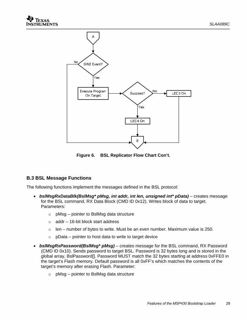
B.2 Implementation
Figure 5 and Figure 6 contain a flow chart for the BSL Replicator application. It illustrates the logic flow for the main program loop. In the figure, an exit from low-power mode 0 (LPM0) occurs after either a Timer_A interrupt or receiving a character from the target BSL.

SLAA089C
28 Features of the MSP430 Bootstrap Loader
Figure 5. BSL Replicator Flow Chart
SLAA089C
Features of the MSP430 Bootstrap Loader 29
Figure 6. BSL Replicator Flow Chart Con’t.
B.3 BSL Message Functions
The following functions implement the messages defined in the BSL protocol:
• bslMsgRxDataBlk(BslMsg* pMsg, int addr, int len, unsigned int* pData) – creates message for the BSL command, RX Data Block (CMD ID 0x12). Writes block of data to target. Parameters:
o pMsg – pointer to BslMsg data structure
o addr – 16-bit block start address
o len – number of bytes to write. Must be an even number. Maximum value is 250.
o pData – pointer to host data to write to target device
• bslMsgRxPassword(BslMsg* pMsg) – creates message for the BSL command, RX Password (CMD ID 0x10). Sends password to target BSL. Password is 32 bytes long and is stored in the global array, BslPassword[]. Password MUST match the 32 bytes starting at address 0xFFE0 in the target’s Flash memory. Default password is all 0xFF’s which matches the contents of the target’s memory after erasing Flash. Parameter:
o pMsg – pointer to BslMsg data structure

SLAA089C
30 Features of the MSP430 Bootstrap Loader
• bslMsgEraseSeg(BslMsg* pMsg, int addr, int len) – creates message for the BSL command, Erase Segment (CMD ID 0x16). Erases specified Flash segment. Parameters:
o pMsg – pointer to BslMsg data structure
o addr – any even-numbered address within the Flash segment to be erased
o len – value of 0xA504 performs erasure of main Flash memory ?????
• bslMsgErase(BslMsg* pMsg) – creates message for the BSL command, Mass Erase (CMD ID 0x18). Erases entire Flash area, both Main and Information Flash. Parameter:
o pMsg – pointer to BslMsg data structure
• bslMsgEraseChk(BslMsg* pMsg, int addr, int len) – creates message for the BSL command, Erase Check (CMD ID 0x1C). Verifies Flash erasure within specified address range. Parameters:
o pMsg – pointer to BslMsg data structure
o addr – any 16-bit block start address (odd or even)
o len – length of block (odd or even)
• bslMsgBaudRate(BslMsg* pMsg, int dco, int bcs, int baudRate) – creates message for the BSL command, Changes Baud Rate (CMD ID 0x20). Parameters:
o pMsg – pointer to BslMsg data structure
o dco – DCO Control Register (DCOCTL) setting for a 1xx device or System Clock Frequency Integrator Register 0 (SCFI0) setting for a 4xx device.
o bcs – Basic Clock System Control Register 1 (BCSCTL1) setting for a 1xx device or System Clock Frequency Integrator Register 1 (SCFI1) setting for a 4xx device.
o baudRate – 0 is 9600 baud, 1 is 19200 baud, and 2 is 38400 baud
• bslMsgLoadPC(BslMsg* pMsg, int addr) – creates message for the BSL command, Load PC (CMD ID 0x1A). Sets target’s program counter register to specified value. Parameters:
o pMsg – pointer to BslMsg data structure
o addr – value for target’s program counter register (R0)
• bslMsgTxDataBlk(BslMsg* pMsg, int addr, int bytes) – creates message for the BSL command, TX Data Block (CMD ID 0x14). Reads block of data from target. Parameters:
o pMsg – pointer to BslMsg data structure
o addr – 16-bit block start address
o bytes – length of block. Maximum value is 250.
• bslMsgVer(BslMsg* pMsg) – creates message for the BSL command, BSL Version (CMD ID 0x1E). Reads BSL version number and MSP430 device information from target. Parameter:
o pMsg – pointer to BslMsg data structure

SLAA089C
Features of the MSP430 Bootstrap Loader 31
B.4 BSL Implementation Functions
The following functions assist with the implementation of the BSL protocol.
• bslEntrySeq(void) – generates BSL entry sequence. If the input signal BSL_SEQ is tied to VCC, then the signals required to place a MSP430 device having dedicated JTAG pins into BSL mode will be generated. If BSL_SEQ is tied low, then the signals required to place a MSP430 device having shared JTAG pins into BSL mode will be generated.
• bslChecksum(BslMsg* pMsg) – generates check sum for BSL message. Parameter:
o pMsg – pointer to BslMsg data structure
• bslTxMsg(BslMsg* pMsg) – transmits message to target BSL. Parameter:
o pMsg – pointer to BslMsg data structure
• bslTxSync(void) – transmits SYNC character to target BSL.
• bslSendChar(unsigned char val) – transmits a single character to target BSL. Parameter:
o val – any 8-bit value
• bslWaitForReply(unsigned char type) – waits for reply from target BSL. The BSL can respond in two ways. It either sends an ACK character or it responds with a message having a specified length. If target BSL does not reply, function returns a timeout error. Parameter:
o type – BSL reply type, BSL_ACK_REPLY or BSL_MSG_REPLY
• bslStateReset(void) – resets host to restart communications with target BSL.
• bslDownloadCode(unsigned int* pCodeArray, unsigned char patchFlag) – downloads code to target BSL. Code can be for BSL patch or target program. Parameters:
o pCodeArray – pointer to host array containing code to download to target
o patchFlag - !0 value indicates BSL patch code is installed on target
• bslDownloadProgram(void) – downloads program to target. Program is stored in Flash memory on host in global array called CodeArray[].
• bslInstallPatch(void) – installs BSL patch on target. Patch is stored in Flash memory on host in global array called PatchArray[].
SLAA089C
32 Features of the MSP430 Bootstrap Loader
B.5 Building a Downloadable MSP430 Application
Perform the following steps to build an application that can be downloaded by the BSL Replicator to program another MSP430 device. The BSL Replicator stores the application locally in the array, CodeArray[].
Creating the Target Source
1. Use IAR’s IDE to create a MSP430 project for the target device.
2. Open the “Options” dialog box for the project by selecting “Project->Options…” from the main menu or by right-clicking on the project and selecting “Options…” on the pop-up menu.
3. Select “Linker” under the section labeled “Category”.
4. Select the “Output” tab.
5. Under the section labeled “Format”, select the radio button labeled “Other”.
6. Select the “msp430-txt” option for the text box labeled “Output format”.
7. Select “OK” and close the “Options” dialog box.
8. Build the project.
9. Convert the “*.txt” project output file into a “*.s43” assembly file using the FileMaker.exe conversion program provided with this application note (Note: when using FileMaker, make sure to select the .s43 output file format).
Creating the BSL Replicator Source
10. Use IAR’s IDE to create a MSP430 project for the Host device (BSL Replicator).
11. Add the “bsl_replicator.c” source file to the BSL Replicator project.
12. Add the “PATCH.s43” source file to the BSL Replicator project if using the BSL patch for the target.
13. Add the converted assembly .s43 output file from Step 9 to the BSL Replicator project.
14. Build the BSL Replicator project and download to the MSP430F149 host.
Programming the Target Device
15. Connect the BSL Replicator to the Target device as shown in Figure 4.
16. Press SW1 to program the Target device.
17. After successful programming, pressing SW2 will release the Target to execute the target program.

IMPORTANT NOTICE
Texas Instruments Incorporated and its subsidiaries (TI) reserve the right to make corrections, modifications,enhancements, improvements, and other changes to its products and services at any time and to discontinueany product or service without notice. Customers should obtain the latest relevant information before placingorders and should verify that such information is current and complete. All products are sold subject to TI’s termsand conditions of sale supplied at the time of order acknowledgment.
TI warrants performance of its hardware products to the specifications applicable at the time of sale inaccordance with TI’s standard warranty. Testing and other quality control techniques are used to the extent TIdeems necessary to support this warranty. Except where mandated by government requirements, testing of allparameters of each product is not necessarily performed.
TI assumes no liability for applications assistance or customer product design. Customers are responsible fortheir products and applications using TI components. To minimize the risks associated with customer productsand applications, customers should provide adequate design and operating safeguards.
TI does not warrant or represent that any license, either express or implied, is granted under any TI patent right,copyright, mask work right, or other TI intellectual property right relating to any combination, machine, or processin which TI products or services are used. Information published by TI regarding third-party products or servicesdoes not constitute a license from TI to use such products or services or a warranty or endorsement thereof.Use of such information may require a license from a third party under the patents or other intellectual propertyof the third party, or a license from TI under the patents or other intellectual property of TI.
Reproduction of information in TI data books or data sheets is permissible only if reproduction is withoutalteration and is accompanied by all associated warranties, conditions, limitations, and notices. Reproductionof this information with alteration is an unfair and deceptive business practice. TI is not responsible or liable forsuch altered documentation.
Resale of TI products or services with statements different from or beyond the parameters stated by TI for thatproduct or service voids all express and any implied warranties for the associated TI product or service andis an unfair and deceptive business practice. TI is not responsible or liable for any such statements.
Following are URLs where you can obtain information on other Texas Instruments products and applicationsolutions:
Products Applications
Amplifiers amplifier.ti.com Audio www.ti.com/audio
Data Converters dataconverter.ti.com Automotive www.ti.com/automotive
DSP dsp.ti.com Broadband www.ti.com/broadband
Interface interface.ti.com Digital Control www.ti.com/digitalcontrol
Logic logic.ti.com Military www.ti.com/military
Power Mgmt power.ti.com Optical Networking www.ti.com/opticalnetwork
Microcontrollers microcontroller.ti.com Security www.ti.com/security
Telephony www.ti.com/telephony
Video & Imaging www.ti.com/video
Wireless www.ti.com/wireless
Mailing Address: Texas Instruments
Post Office Box 655303 Dallas, Texas 75265
Copyright 2006, Texas Instruments Incorporated


![Vortrag zur Seminarphase der PG „Solar Doorplate“ MSP430 ... · MSP430 – Wichtigste Grundlagen von David Tondorf. 2 ... MSP430 microcontroller basics. Oxford: Newnes [4] MSP430](https://img.dokumen.tips/doc/110x75/5b6f6a9b7f8b9af12d8c481e/vortrag-zur-seminarphase-der-pg-solar-doorplate-msp430-msp430-.jpg)

![[MSP430] GPIO](https://img.dokumen.tips/doc/110x75/55cf9df0550346d033aff200/msp430-gpio.jpg)
![[MSP430] ADC10](https://img.dokumen.tips/doc/110x75/55cf97c5550346d033938430/msp430-adc10-5654b9a37ede3.jpg)