Embed Size (px)
Citation preview

1
LECTURE NOTES
ON
VLSI DESIGN
B.Tech VII semester (R16)
Mr.V.R Seshagiri Rao , Associate Professor
Dr. V Vijay, Associate Professor
Dr. M Manisha, Associate Professor
Ms K.S.Indrani, Assistant Professor
ELECTRONICS AND COMMUNICATION ENGINEERING
INSTITUTE OF AERONAUTICAL ENGINEERING
(Autonomous) DUNDIGAL, HYDERABAD - 500043

2
UNIT-I
MOSFETS

3
Fundamentals of MOSFETs
In 1958, Jack Kilby built the first integrated circuit flip-flop with two transistors at Texas Instruments. In 2008,
Intel’s Itanium microprocessor contained more than 2 billion transistors and a 16 Gb Flash memory contained
more than 4 billion transistors. This corresponds to a compound annual growth rate of 53% over 50 years. No
other technology in history has sustained such a high growth rate lasting for so long.
This incredible growth has come from steady miniaturization of transistors and improvements in manufacturing
processes. Most other fields of engineering involve tradeoffs between performance, power, and price. However,
as transistors become smaller, they also become faster, dissipate less power, and are cheaper to manufacture.
This synergy has not only revolutionized electronics, but also society at large. The processing performance once
dedicated to secret government supercomputers is now available in disposable cellular telephones. The memory
once needed for an entire company’s accounting system is now carried by a teenager in her iPod. Improvements
in integrated circuits have enabled space exploration, made automobiles safer and more fuel efficient,
revolutionized the nature of warfare, brought much of mankind’s knowledge to our Web browsers, and made
the world a flatter place. Fig. 1.1 shows annual sales in the worldwide semiconductor market. Integrated circuits
became a $100 billion/year business in 1994. In 2007, the industry manufactured approximately 6 quintillion (6
× 1018
) transistors, or nearly a billion for every human being on the planet. Thousands of engineers have made
their fortunes in the field. New fortunes lie ahead for those with innovative ideas and the talent to bring those
ideas to reality. During the first half of the twentieth century, electronic circuits used large, expensive, power-
hungry, and unreliable vacuum tubes. In 1947, John Bardeen and Walter Brattain built the first functioning
point contact transistor at Bell Laboratories. It was nearly classified as a military secret, but Bell Labs publicly
introduced the device the following year.
Fig 1.1
Ten years later, Jack Kilby at Texas Instruments realized the potential for miniaturization if multiple transistors
could be built on one piece of silicon. Figure 1.2(b) shows his first prototype of an integrated circuit,
constructed from a germanium slice and gold wires. The invention of the transistor earned the Nobel Prize in
Physics in 1956 for Bardeen, Brattain, and their supervisor William Shockley. Kilby received the Nobel Prize in
Physics in 2000 for the invention of the integrated circuit. Transistors can be viewed as electrically controlled
switches with a control terminal and two other terminals that are connected or disconnected depending on the
voltage or current applied to the control. Soon after inventing the point contact transistor, Bell Labs developed
the bipolar junction transistor. Bipolar transistors were more reliable, less noisy, and more power-efficient.

4
FIGURE 1.2 (a) First transistor (Property of AT&T Archives. Reprinted with permission of AT&T.) and (b)
first integrated circuit (Courtesy of Texas Instruments.)
Early integrated circuits primarily used bipolar transistors. Bipolar transistors require a small current into the
control (base) terminal to switch much larger currents between the other two (emitter and collector) terminals.
The quiescent power dissipated by these base currents, drawn even when the circuit is not switching, limits the
maximum number of transistors that can be integrated onto a single die. By the 1960s, Metal Oxide
Semiconductor Field Effect Transistors (MOSFETs) began to enter production. MOSFETs offer the compelling
advantage that they draw almost zero control current while idle. They come in two flavors: nMOS and pMOS,
using n-type and p-type silicon, respectively. The original idea of field effect transistors dated back to the
German scientist Julius Lilienfield in 1925 and a structure closely resembling the MOSFET was proposed in
1935 by Oskar Heil . but materials problems foiled early attempts to make functioning devices. In 1963, Frank
Wanlass at Fairchild described the first logic gates using MOSFETs . Fairchild’s gates used both nMOS and
pMOS transistors, earning the name Complementary Metal Oxide Semiconductor, and CMOS. The circuits
used discrete transistors but consumed only nanowatts of power, six orders of magnitude less than their bipolar
counterparts. With the development of the silicon planar process, MOS integrated circuits became attractive for
their low cost because each transistor occupied less area and the fabrication process was simpler . Early
commercial processes used only pMOS transistors and suffered from poor performance, yield, and reliability.
Processes using nMOS transistors became common in the 1970s . Intel pioneered nMOS technology with its
1101 256-bit static random access memory and 4004 4-bit microprocessor, as shown in Figure 1.1. While the
nMOS process was less expensive than CMOS, nMOS logic gates still consumed power while idle. Power
consumption became a major issue in the 1980s as hundreds of thousands of transistors were integrated onto a
single die. CMOS processes were widely adopted and have essentially replaced nMOS and bipolar processes
for nearly all digital logic applications. In 1965, Gordon Moore observed that plotting the number of transistors
that can be most economically manufactured on a chip gives a straight line on a semilogarithmic scale . At the
time, he found transistor count doubling every 18 months. This observation has been called Moore’s Law and
has become a self-fulfilling prophecy. Figure 1.1 shows that the number of transistors in Intel microprocessors
has doubled every 26 months since the invention of the 4004. Moore’s Law is driven primarily by scaling down
the size of transistors and, to a minor extent, by building larger chips. The level of integration of chips has been
classified as small-scale, medium-scale, large-scale, and very large scale. Small-scale integration (SSI) circuits,
such as the 7404 inverter, have fewer than 10 gates, with roughly half a dozen transistors per gate. Medium-
scale integration (MSI) circuits, such as the 74161 counter, have up to 1000 gates. Large-scale integration

5
(LSI) circuits, such as simple 8-bit microprocessors, have up to 10,000 gates. It soon became apparent that new
names would have to be created every five years if this naming trend continued and thus the term very large-
scale integration (VLSI) is used to describe most integrated circuits from the 1980s onward. A corollary of
Moore’s law is Dennard’s Scaling Law [Dennard74]: as transistors shrink, they become faster, consume less
power, and are cheaper to manufacture. Intel microprocessor clock frequencies have doubled roughly every 34
months.This frequency scaling hit the power wall around 2004, and clock frequencies have leveled off around 3
GHz. Computer performance, measured in time to run an application, has advanced even more than raw clock
speed. Presently, the performance is driven by the number of cores on a chip rather than by the clock. Even
though an individual CMOS transistor uses very little energy each time it switches, the enormous number of
transistors switching at very high rates of speed has made power consumption a major design consideration
again. Moreover, as transistors have become so small, they cease to turn completely OFF. Small amounts of
current leaking through each transistor now lead to significant power consumption when multiplied by millions
or billions of transistors on a chip. The feature size of a CMOS manufacturing process refers to the minimum
dimension of a transistor that can be reliably built. The 4004 had a feature size of 10 µm in 1971. The Core 2
Duo had a feature size of 45 nm in 2008. Manufacturers introduce a new process generation (also called a
technology node) every 2–3 years with a 30% smaller feature size to pack twice as many transistors in the same
area. Feature sizes down to 0.25 µm are generally specified in microns (10–6
m), while smaller feature sizes are
expressed in nanometers (10–9
m). Effects that were relatively minor in micron processes, such as transistor
leakage, variations in characteristics of adjacent transistors, and wire resistance, are of great significance in
nanometer processes. Moore’s Law has become a self-fulfilling prophecy because each company must keep up
with its competitors. Obviously, this scaling cannot go on forever because transistors cannot be smaller than
atoms. Dennard scaling has already begun to slow. By the 45 nm generation, designers are having to make
trade-offs between improving power and improving delay. Although the cost of printing each transistor goes
down, the one-time design costs are increasing exponentially, relegating state-of-the-art processes to chips that
will sell in huge quantities or that have cutting-edge performance requirements. However, many predictions of
fundamental limits to scaling have already proven wrong. Creative engineers and material scientists have
billions of dollars to gain by getting ahead of their competitors. In the early 1990s, experts agreed that scaling
would continue for at least a decade but that beyond that point the future was murky. In 2009, we still believe
that Moore’s Law will continue for at least another decade. The future is yours to invent.
Basics of MOSFET:
A Metal-Oxide-Semiconductor (MOS) structure is created by superimposing several layers of conducting and
insulating materials to form a sandwich-like structure. These structures are manufactured using a series of
chemical processing steps involving oxidation of the silicon, selective introduction of dopants, and deposition
and etching of metal wires and contacts. Transistors are built on nearly flawless single crystals of silicon, which
are available as thin flat circular wafers of 15–30 cm in diameter. CMOS technology provides two types of
transistors (also called devices): an n-type transistor (nMOS) and a p-type transistor (pMOS). Transistor
operation is controlled by electric fields so the devices are also called Metal Oxide Semiconductor Field Effect
Transistors (MOSFETs) or simply FETs. Cross-sections and symbols of these transistors are shown in Figure
1.3. The n+ and p+ regions indicate heavily doped n- or p-type silicon.
Each transistor consists of a stack of the conducting gate, an insulating layer of silicon dioxide (SiO2, better

6
known as glass), and the silicon wafer, also called the substrate, body, or bulk. Gates of early transistors were
built from metal, so the stack was called metaloxide- semiconductor, or MOS.
FIGURE 1.3 nMOS transistor and pMOS transistor
Since the 1970s, the gate has been formed from polycrystalline silicon (polysilicon), but the name stuck.
(Interestingly, metal gates reemerged in 2007 to solve materials problems in advanced manufacturing
processes.) An nMOS transistor is built with a p-type body and has regions of n-type semiconductor adjacent to
the gate called the source and drain. They are physically equivalent and for now we will regard them as
interchangeable. The body is typically grounded. A pMOS transistor is just the opposite, consisting of p-type
source and drain regions with an n-type body. In a CMOS technology with both flavors of transistors, the
substrate is either n-type or p-type. The other flavor of transistor must be built in a special well in which dopant
atoms have been added to form the body of the opposite type. The gate is a control input: It affects the flow of
electrical current between the source and drain. Consider an nMOS transistor. The body is generally grounded
so the p–n junctions of the source and drain to body are reverse-biased. If the gate is also grounded, no current
flows through the reverse-biased junctions. Hence, we say the transistor is OFF. If the gate voltage is raised, it
creates an electric field that starts to attract free electrons to the underside of the Si–SiO2 interface. If the
voltage is raised enough, the electrons outnumber the holes and a thin region under the gate called the channel
is inverted to act as an n-type semiconductor. Hence, a conducting path of electron carriers is formed from
source to drain and current can flow. We say the transistor is ON. For a pMOS transistor, the situation is again
reversed. The body is held at a positive voltage. When the gate is also at a positive voltage, the source and drain
junctions are reverse-biased and no current flows, so the transistor is OFF. When the gate voltage is lowered,
positive charges are attracted to the underside of the Si–SiO2 interface. A sufficiently low gate voltage inverts
the channel and a conducting path of positive carriers is formed from source to drain, so the transistor is ON.
Notice that the symbol for the pMOS transistor has a bubble on the gate, indicating that the transistor behavior
is the opposite of the nMOS. The positive voltage is usually called VDD or POWER and represents a logic 1
value in digital circuits. In popular logic families of the 1970s and 1980s, VDD was set to 5 volts. Smaller, more
recent transistors are unable to withstand such high voltages and have used supplies of 3.3 V, 2.5 V, 1.8 V, 1.5
V, 1.2 V, 1.0 V, and so forth. The low voltage is called GROUND (GND) or VSS and represents a logic 0. It is
normally 0 volts. In summary, the gate of an MOS transistor controls the flow of current between the source
and drain. Simplifying this to the extreme allows the MOS transistors to be viewed as simple ON/OFF switches.
When the gate of an nMOS transistor is 1, the transistor is ON and there is a conducting path from source to
drain. When the gate is low, the nMOS transistors are OFF and almost zero current flows from source to drain.
A pMOS transistor is just the opposite, being ON when the gate is low and OFF when the gate is high. This

7
switch model is illustrated in Figure 1.4, where g, s, and d indicate gate, source, and drain. This model will be
our most common one when discussing circuit behavior.
FIGURE 1.4 Transistor symbols and switch-level models
Even when transistors are nominally OFF, they leak small amounts of current. Leakage mechanisms include
subthreshold conduction between source and drain, gate leakage from the gate to body, and junction leakage
from source to body and drain to body, as illustrated in Figure 2.19 [Roy03, Narendra06]. Subthreshold
conduction is caused by thermal emission of carriers over the potential barrier set by the threshold. Gate leakage
is a quantum-mechanical effect caused by tunneling through the extremely thin gate dielectric.Junction leakage
is caused by current through the p-n junction between the source/drain diffusions and the body.
In processes with feature sizes above 180 nm, leakage was typically insignificant except in very low power
applications. In 90 and 65 nm processes, threshold voltage has reduced to the point that subthreshold leakage
reaches levels of 1s to 10s of nA per transistor,which is significant when multiplied by millions or billions of
transistors on a chip.In 45 nm processes, oxide thickness reduces to the point that gate leakage becomes
comparable to subthreshold leakage unless high-k gate dielectrics are employed. Overall, leakage has become
an important design consideration in nanometer processes.
Subthreshold Leakage The long-channel transistor I-V model assumes current only flows from source to drain
when Vgs Vt. In real transistors, current does not abruptly cut off below threshold, but rather drops off
exponentially, as seen in Figure 2.20. When the gate voltage is high, the transistor is strongly ON. When the
gate falls below Vt , the exponential decline in current appears as a straight line on the logarithmic scale. This
regime of Vgs <Vt is called weak inversion. The subthreshold leakage current increases significantly with Vds
because of drain-induced barrier lowering. There is a lower limit on Ids set by drain junction leakage that is
exacerbated by the negative gate voltage.
MOSFETs in the Sub-threshold Region (i.e. a bit below VT)
In the depletion approximation for n-channel MOS structures we have neglected the electrons beneath the gate
electrode when the gate voltage is less than the threshold voltage, VT. We said that it is only when the gate
voltage is above threshold that they are significant, and that they are then the dominant negative charge under
the gate. Furthermore, we say that above threshold all of the gate voltage in excess of VT induces electrons in
the channel.
As MOS integrated circuit technology has evolved to exploit smaller and smaller device structures, it has
become increasingly important in recent years to look more closely at the minority carriers present under the
gate when the gate voltage is less than threshold, i.e. in what is called the “sub-threshold” region. These carriers
cannot be totally neglected, and play an important role in device and circuit performance. At first they were
viewed primarily as a problem, causing undesirable “leakage” currents and limiting circuit performance. Now it

8
is recognized that they also enable a very useful mode of MOSFET operation, and that the sub- threshold region
of operation is as important as the traditional cut-off, linear, and saturations regions of operation. To begin our
study of the sub-threshold region, we will first quickly review the electrostatics of the MOS capacitor, and the
electrostatic potential profile predicted by the depletion approximation model.
Fig 1.5
Then we will use this result to derive a more accurate expression than that in Equation 1 for qN* below
threshold, and use the resulting expression to, among other things, assess the assumption that the contribution of
the mobile electrons underneath the gate to the net charge density in the depletion region is negligible compared
to the contribution from the ionized acceptors. Finally we will look at the current-voltage characteristic of a
MOSFET operating in the sub-threshold region, and merge it with our earlier model so that we then have a
model in which the mobile electron charge is taken into account and the drain current is no longer identically
zero when vGS is less than VT.

9
FIGURE 1.6
The electron sheet charge density under the gate with a gate voltage in the vicinity of threshold. The blue curve
corresponds to the sub-threshold weak-inversion charge [Eq. 12], and the red curve is the strong inversion
charge from traditional depletion approximation modeling. The sum is plotted in the yellow curve.
The MOSFET Drain Current in the Sub-threshold Region:
FIGURE 1.7
The drain current, iD, for gate biases from just below to just above threshold illustrating the relative sizes of the
diffusion (sub-threshold) and drift (strong inversion) components of iD. Figure 1.7 a shows the situation with a
course voltage scale, while Figure 1.7 b has smaller increments and thus focuses in more on the curves near VT.

10
FIGURE 1.8
The drain current, iD, for gate biases from just below to just above threshold as in Figure 1.7b, but now plotted
on a log-linear graph so the nature of the small, sub-threshold current and its variation with input voltage, VGS,
is more clear. The simple depletion approximation model we are using, our neglect of drift currents below
threshold, and our use of a saturated diffusion current above threshold, are all reasonable approximations, and
are better the further we are above or below threshold. We should expect them to have limitations very near
threshold, however, and in particular we should not demand too much from them as we pass from vGS < VT to
vGS > VT. The curves look rather smooth in Figure 1.7 b, but we see a slight kink on the log scale of Figure 1.8.
Interestingly, this kink can be smoothed nicely by using the adjusted threshold in the saturation current
expression, as shown in Fig. 1.8, but is largely coincidence as the 6 mV shift came from looking at the total gate
charge in the sub-threshold region, not the inversion layer in strong inversion. Just the same, our simple models
accurately reflect the physics, and do an outstanding job no matter how one looks at it.
ENHANCEMENT AND DEPLETION MODE MOS TRANSISTORS
MOS Transistors are built on a silicon substrate. Silicon which is a group IV material is the eighth most
common element in the universe by mass, but very rarely occurs as the pure free element in nature. Pure silicon
has no free carriers and conducts poorly. But adding dopants to silicon increases its conductivity. If a group V
material i.e. an extra electron is added, it forms an n-type semiconductor. If a group III material i.e. missing
electron pattern is formed (hole), the resulting semiconductor is called a p-type semiconductor.
A junction between p-type and n-type semiconductor forms a conduction path. Source and Drain of the Metal
Oxide Semiconductor (MOS) Transistor is formed by the “doped” regions on the surface of chip. Oxide layer is
formed by means of deposition of the silicon dioxide (SiO2) layer which forms as an insulator and is a very thin
pattern.
Gate of the MOS transistor is the thin layer of “polysilicon (poly)”; used to apply electric field to the surface of
silicon between Drain and Source, to form a “channel” of electrons or holes. Control by the Gate voltage is
achieved by modulating the conductivity of the semiconductor region just below the gate. This region is known
as the channel. The Metal–Oxide–Semiconductor Field Effect Transistor (MOSFET) is a transistor which is a
voltage-controlled current device, in which current at two electrodes, drain and source is controlled by the
action of an electric field at another electrode gate having in-between semiconductor and a very thin metal
oxide layer. It is used for amplifying or switching electronic signals. The Enhancement and Depletion mode
MOS transistors are further classified as N-type named NMOS (or N-channel MOS) and P-type named PMOS
(or P-channel MOS) devices. Figure 1.9 shows the MOSFETs along with their enhancement and depletion

11
modes.
Figure 1.9: (c) Enhancement P-type MOSFET (d) Depletion P-type MOSFET
The depletion mode devices are doped so that a channel exists even with zero voltage from gate to source
during manufacturing of the device. Hence the channel always appears in the device. To control the channel, a
negative voltage is applied to the gate (for an N-channel device), depleting the channel, which reduces the
current flow through the device. In essence, the depletion-mode device is equivalent to a closed (ON) switch,
while the enhancement-mode device does not have the built in channel and is equivalent to an open (OFF)
switch. Due to the difficulty of turning off the depletion mode devices, they are rarely used
Working of Enhancement Mode Transistor The enhancement mode devices do not have the in-built channel.
By applying the required potentials, the channel can be formed. Also for the MOS devices, there is a threshold
voltage (Vt), below which not enough charges will be attracted for the channel to be formed. This threshold
voltage for a MOS transistor is a function of doping levels and thickness of the oxide layer.
Case 1: Vgs = 0V and Vgs < Vt The device is non-conducting, when no gate voltage is applied (Vgs = 0V) or
(Vgs < Vt) and also drain to source potential Vds = 0. With an insufficient voltage on the gate to establish the
channel region as N-type, there will be no conduction between the source and drain. Since there is no
conducting channel, there is no current drawn, i.e. Ids = 0, and the device is said to be in the cut-off region.
This is shown in the Figure 1.7 (a).

12
Figure 2.0 (a)
Case 2: Vgs > Vt When a minixmum voltage greater than the threshold voltage Vt (i.e. Vgs > Vt) is applied, a
high concentration of negative charge carriers forms an inversion layer located by a thin layer next to the
interface between the semiconductor and the oxide insulator. This forms a channel between the source and drain
of the transistor. This is shown in the Figure 2.0 (b).
Figure 2.0: (b) Formation of a Channel
A positive Vds reverse biases the drain substrate junction, hence the depletion region around the drain
widens, and since the drain is adjacent to the gate edge, the depletion region widens in the channel. This is
shown in Figure 2.0(c). This results in flow of electron from source to drain resulting in current Ids.. The device
is said to operate in linear region during this phase. Further increase in Vds, increases the reverse bias on the
drain substrate junction in contact with the inversion layer which causes inversion layer density to decrease.
This is shown in Figure 2.0 (d). The point at which the inversion layer density becomes very small (nearly zero)
at the drain end is termed pinch-off. The value of Vds at pinch-off is denoted as Vds,sat. This is termed as
saturation region for the MOS device. Diffusion current completes the path from source to drain in this case,
causing the channel to exhibit a high resistance and behaves as a constant current source.
The MOSFET ID versus VDS characteristics (V-I Characteristics) is shown in the Figure 2.0.
For VGS < Vt, ID = 0 and device is in cut-off region. As VDS increases at a fixed VGS, ID increases in the
linear region due to the increased lateral field, but at a decreasing rate since the inversion layer density is
decreasing. Once pinch-off is reached, further increase in VDS results in increase in ID; due to the formation of
the high field region which is very small. The device starts in linear region, and moves into saturation region at
higher VDS.

13
The MOSFET transistor has become one of the most important devices used in the design and construction
of integrated circuits. Its thermal stability and other general characteristics make it extremely popular
in computer circuit design.The basic principle of the MOSFET is that the source-to-drain current(SD
current) is controlled by the gate voltage, or better, by the gate electric field. The electric field indices
charge (field effect) in tahe semiconductor at the semiconductor –oxide interface.Thus the MOSFET is a
voltage-controlled current source.
Basic MOS transistors with the doping concentration of transistor two types of MOS transistors are
available as NMOS transistor and PMOS transistor. With their mode of operation further they are classified
as depletion mode transistor and enhancement mode transistor.
NMOS enhancement mode transistor
nMOS devices are formed in a p-type substrate of moderate doping level. The source and drain regions are
formed by diffusing n-type impurities through suitable masks into these areas. Thus source and drain are
isolated from one another by two diodes and their Connections are made by a deposited metal layer.
The basic block diagrams of nMOS enhancement mode transistor is shown in figure.
Fig 2.1
If the gate terminal is connected to a positive voltage(a minimum voltage level of threshold
voltage) with respect to the source, then the electric field established between the gate and the substrate which
gives a charge inversion region in the substrate under the gate insulation and a conduction path or channel is
formed between source and drain, but no current flows between source and drain(Vds=0) .When current flows
in the channel by applying a voltage Vds between source and drain there must bea voltage(IR) drop = Vds
along the channel.
This results that the voltage between gate and channel varying with distance along the channel with the voltage
being a maximum of Vgs at the source end. The effective gate voltage is Vg = Vgs - Vt .To invert the
channel at the drain end there will be voltage is available upto when Vgs-Vt > Vds.• For all voltages Vds <
Vgs - Vt the device is in the non-satrurated region.

14
Fig 2.2
When Vds is increased to a level greater than Vgs - Vt,, if the voltage drop = Vgs - Vt takes place over
less than the whole length of the channel near the drain, there is insufficient electric field available to give
rise to an inversion layer to create the channel. Then the voltage is called ‘pinch-off’ voltage. At this stage
the diffusion current completes the path from source to drain and the channel exhibits a high resistance and
behave as constant current source, This region is known as ‘saturation’ region.
nMOS depletion mode transistor
The basic block diagram of nMOS depletion mode transistor is shown in figure. In depletion mode
transistor the channel is established even the voltage Vgs = 0 by implanting suitable impurities in the
region between source and drain during manufacture and prior to depositing the insulation and the gate.
Fig 2.3
At this stage the source and drain are connected by a conducting channel, but the channel may now be closed
by applying a suitable negative voltage to the gate. In both enhancement and depletion mode cases,
variations of the gate voltage allow control of any current flow between source and drain.
DRAIN-TO-SOURCE CURRENT Ids versus VOLTAGE Vds RELATIONSHIPS)
The whole concept of the MOS transistor evolves from the use of a voltage on the gate to induce a charge in the
channel between source and drain, which may then be caused to move from source to drain under the influence of
an electric field created by voltage V ds applied between drain and source. Since the charge induced is dependent
on the gate to source voltage Vgs• then Ids is dependent on both Vgs and Vds· Consider a structure, as in Figure
2.1, in which" electrons will flow source to drain:

15

16

17

18

19

20
MOSFET parasitic capacitances :
These are subdivided into two general categories:
1. extrinsic capacitances
2. intrinsic capacitances.
Extrinsic capacitances are associated with regions of the transistor outside the dashed line.
Intrinsic capacitances are all those capacitances located within the boxed region.

21
EXTRINSIC CAPACITANCES
Extrinsic capacitances are modeled by using lumped capacitances, each of which is associated with a region
of the transistor’s geometry.One capacitor is used between each pair of transistor terminals, plus an
additional capacitor between the well and the bulk if the transistor is fabricated in a well.
Extrinsic Capacitance Types
Overlap capacitances that are mostly dependent on geometry.
Junction capacitances that are dependent on geometry and on bias.

22

23
Diode Capacitance
When a reverse voltage is applied to a PN junction , the holes in the p-region are attracted to the anode
terminal and electrons in the n-region are attracted to the cathode terminal. The resulting region contains
almost no carriers, and is called the depletion region. The depletion region acts similarly to the dielectric of a
capacitor.The depletion region increases in width as the reverse voltage across it increases. If we imagine
that the diode capacitance can be likened to a parallel plate capacitor, then as the plate spacing (i.e. the
depletion region width) increases, the capacitance should decrease. Increasing the reverse bias voltage across
the PN junction therefore decreases the diode capacitance. Source/Drain-Bulk Junction Capacitances At the
source region there is a source-to bulk junction capacitance, CjBS,e, and at the drain region there is a drain-
to-bulk junction capacitance, CjBD,e. Source/Drain-Bulk Junction Capacitances The junction capacitances
can be calculated by splitting the drain and source regions into a “side-wall” portion and a “bottom-wall”
portion. n The capacitance associated with the side wall portion is found by multiplying the length of the
side-wall perimeter (excluding the side contacting the channel) by the effective sidewall capacitance per unit
length. The capacitance for the bottom-wall portion is found by multiplying the area of the bottomwall by the
bottom-wall capacitance per unit area. Well-Bulk Junction Capacitance If the MOSFET is in a well, a well-
to-bulk junction capacitance, CjBW,e, must be added. The well-bulk junction capacitance is calculated
similarly to the source and drain junction capacitances, by dividing the total well-bulk junction capacitance
into side-wall and bottom-wall components. If more than one transistor is placed in a well, the well-bulk
junction capacitance should only be included once in the total model.

24
UNIT-II
VLSI Design styles

25
nMOS FABRICATION
Fabrication is the process to create the devices and wires on a single silicon chip.
•The process starts with a silicon substrate of high purity into which the required p-impurities are
introduced.
•A layer of silicon dioxide(sio2) is grown all over the surface of the wafer to protect the
surface and acts as a barrier to dopants during processing and provide a generally insulating
substrate onto which other layers may be deposited and patterned.
The surface is now covered with a photoresist which is deposited onto
the wafer and spun to achieve an even distribution of the required thickness.
• The photoresist layer is then exposed to ultraviolet light through a mask which efines those
regions into which diffusion is to take place together with transistor channels.

26
•These areas are subsequently readily etched away together with the underlying silicon dioxide so
that the wafer surface is exposed in the window defined by the mask.
•The remaining photoresist is removed and a thin layer of sio2 is grown over the entire chip surface
and then polysilicon is deposited on top of this to form the gate structure.
•The polysilicon layer consists of heavily doped polysilicon deposited by chemical vapour
deposition(CVD),

27
•Further photoresist coating and masking allows the polysilicon to be patterned and then the thin
oxide is removed to exposed areas into which n-type impurities are to be diffused to form the source
and drain.
•Diffusion is achieved by heating the wafer to a high temperature and passing a gas containing the
desired n-type impurity over the surface.
•Thick oxide (sio2) is grown over all again and is then masked with photoresist and etched to
expose selected aareas of the polysilicon gate and the drain and source areas where connections area
to be made.

28
•The whole chip then has metal deposited over the surface to a thickness typically of 1µm. This
metal layer is then masked and etched to form the required interconnection pattern.
cMOS fabrication
CMOS Technology depends on using both N-Type and P-Type devices on the same chip.
The two main technologies to do this task are:
• P-Well (Will discuss the process steps involved with this technology)
•The substrate is N-Type. The N-Channel device is built into a P-Type well within the parent N-
Type substrate. The P-channel device is built directly on the substrate.
•N-Well
•The substrate is P-Type. The N-channel device is built directly on the substrate, while the P-
channel device is built
•Two more advanced technologies to do this task are:Becoming more popular for sub-micron
geometries where device performance and density must be pushed beyond the limits of the
conventional p & n-well CMOS processes.
•Twin Tub
•Both an N-Well and a P-Well are manufactured on a lightly doped N-type substrate.
•Silicon-on-Insulator (SOI) CMOS Process
•SOI allows the creation of independent, completely isolated nMOS and pMOS transistors
virtually side-by-side on an insulating substrate.
The simplified process sequence for the fabrication of CMOS integrated circuits on a p- type
silicon substrate is shown.
•The process starts with the creation of the n-well regions for pMOS transistors, by impurity
implantation into the substrate.
Then, a thick oxide is grown in the regions surrounding the nMOS and pMOS
active regions.
•The thin gate oxide is subsequently grown on the surface through thermal oxidation.
•These steps are followed by the creation of n+ and p+ regions (source, drain and channel-stop
implants).
•Finally the metallization is created (creation of metal interconnects).

29
n-well process
• The n-well CMOS process starts with a moderately doped (impurity concentration
~1016
/cm3) p-type silicon substrate. Then, an initial thick “field” oxide layer (5000A) is grown on
the entire surface.
•The first lithographic mask defines the n-well region. Donor atoms, usually phosphorus, are
implanted through this window in the oxide. Once the n-well is created, the active areas of the
nMOS and pMOS transistors can be defined.
•Following the creation of the n-well region, a thick field oxide is grown around the transistor
active regions, and a thin gate oxide (25A) is grown on top of the active regions
•The polysilicon layer (3000A) is deposited using chemical vapor deposition (CVD) and
patterned by dry plasma etching. The created polysilicon lines will function as the gate
electrodes of the nMOS and the pMOS transistors and their interconnects
•Using a set of two masks, the n+ and p+ Source and Drain regions are implanted into the
substrate and into the n- well, respectively.
•The ohmic contacts to the substrate and to the n-well are implanted in this process step
•An insulating silicon dioxide layer is deposited over the entire wafer using CVD
(5000A). This is for passivation, the protection of all the active components from
contamination.
•The contacts are defined and etched away to expose the silicon or polysilicon contact windows.

30
These contact windows are necessary to complete the circuit interconnections using the metal
layer, which is patterned in the next step.
•Metal (aluminum, >5000A) is deposited over the entire chip surface using metal
evaporation, and the metal lines are patterned through etching.
•Since the wafer surface is non-planar, the quality and the integrity of the metal lines created in
this step are very critical and are ultimately essential for circuit reliability.
•The composite layout and the resulting cross-sectional view of the chip, showing one nMOS
and one pMOS transistor (built-in n-well), the polysilicon and metal interconnections.
•The final step is to deposit a full SiO2 passivation layer (5000A), for protection, over the chip,
except for wire-bonding pad areas.
•
p-well process
•P-well on N-substrate
•N-type substrate
•Oxidation, and mask (MASK 1) to create P-well (4-5µm deep)

31
•P-well doping
•P-well acts as substrate for nMOS devices.
•The two areas are electrically isolated using thick field oxide (and often
•isolation implants [not shown here])
Polysilicon Gate Formation
•Remove p-well definition oxide
•Grow thick field oxide
•Pattern (MASK 2) to expose nMOS and pMOS active regions
•Grow thin layer of SiO2 (~0.1µm) gate oxide, over the entire chip surface
•Deposit polysilicon on top of gate oxide to form gate structure
•Pattern poly on gate oxide (MASK 3)
• nMOS P+ Source/Drain difusion – self-aligned to Poly gate
• Implant P+
nMOS S/D regions (MASK 4)

32
•pMOS N+ Source/Drain difusion – self-aligned to Poly gate
•Implant N+
pMOS S/D regions (MASK 5 – often the inverse of MASK 4)
•pMOS N+ Source/Drain difusion, contact holes & metallisation
•Oxide and pattern for contact holes (MASK 6)
•Deposit metal and pattern (MASK 7)
•Passivation oxide and pattern bonding pads (MASK 8)
•P-well acts as substrate for nMOS devices.
•Two separate substrates : requires two separate substrate connections
•Definition of substrate connection areas can be included in MASK 4/MASK5

33
Twin-Tub (Twin-Well) CMOS Process
This technology provides the basis for separate optimization of the nMOS and pMOS transistors,
thus making it possible for threshold voltage, body effect and the channel transconductance of
both types of transistors to be tuned independently. Generally, the starting material is a n+ or p+
substrate, with a lightly doped epitaxial layer on top. This epitaxial layer provides the actual
substrate on which the n-well and the p-well are formed. Since two independent doping steps are
performed for the creation of the well regions, the dopant concentrations can be carefully
optimized to produce the desired device characteristics. The Twin-Tub process is shown below.
In the conventional p & n‐well CMOS process, the doping density of the well region is typically about
one order of magnitude higher than the substrate, which, among other effects, results in unbalanced drain
parasitics. The twin‐tub process avoids this problem.
Noise Margin
Noise margin is closely related to the DC voltage characteristics [Wakerly00]. This parameter allows you to
determine the allowable noise voltage on the input of a gate so that the output will not be corrupted. The
specification most commonly used to describe noise margin (or noise immunity) uses two parameters: the
LOW noise margin, NML, and the HIGH noise margin, NMH., NML is defined as the difference in maximum
LOW input voltage recognized by the receiving gate and the maximum LOW output voltage produced by the
driving gate.
The value of NMH is the difference between the minimum HIGH output voltage of the driving gate and the
minimum HIGH input voltage recognized by the receiving gate.
Thus,

34
where
VIH = minimum HIGH input voltage
VIL = maximum LOW input voltage
VOH= minimum HIGH output voltage
VOL = maximum LOW output voltage
Inputs between VIL and VIH are said to be in the indeterminate region or forbidden zone and do not
represent legal digital logic levels. Therefore, it is generally desirable to have VIH as close as possible to VIL
and for this value to be midway in the “logic swing,” VOL to VOH. This implies that the transfer
characteristic should switch abruptly; that is, there should be high gain in the transition region. For the
purpose of calculating noise margins, the transfer characteristic of the inverter and the definition of voltage
levels VIL, VOL, VIH, and VOH are shown in Figure above. Logic levels are defined at the unity gain point
where the slope is –1. This gives a conservative bound on the worst case static noise margin .
THE nMOS INVERTER
A basic requirement for producing a complete range of logic circuits is the inverter. This is needed for
restoring logic levels, for Nand and Nor gates, and for sequential and memory circuits of various forms . The
basic inverter circuit requires a transistor with source connected to ground and a load resistor of some sort
connected from the drain to the positive supply rail Vvv· The output is taken from the drain and the input
applied between gate and ground. Resistors are not conveniently produced on the silicon substrate; even
modest values occupy excessively large areas so that some other form of load resistance is required. A
convenient way to solve this problem is to use a depletion mode transistor as the load, as
shown in Figure 2.5.

35
• With no current drawn from the output, the currents Ids for both transistors must be equal.
• For the depletion mode transistor, the gate is connected to the source so it is always on and only the
characteristic curve Vgs = 0 is relevant.
• In this configuration the depletion mode device is called the pull-up (p.u.) and the enhancement mode
device the pull-down (p.d.) transistor.
• To obtain the inverter transfer characteristic we superimpose the Vgs = 0 depletion mode characteristic
curve on the family of curves for the enhancement mode device,noting that maximum voltage across the
enhancement mode device corresponds to minimum voltage across the depletion mode transistor.
• The points of intersection of the curves as in Figure f-6 give points on the transfer characteristic, which is
of the form shown in Figure 2.7.
• Note that as Vin(=Vgs p.d. transistor) exceeds the p.d. threshold voltage current begins to flow. The output
voltage Vout thus decreases and the subsequent increases in Vin will cause the p.d. transistor to come out of
saturation and become resistive. Note that the p.u. transistor is initially resistive as the p.d. turns on.

36
during transition, the slope of the transfer characteristic determines the gain:(.fl
THE CMOS INVERTER
(a) No current flow either for logical 0 or for logical 1 inputs.
(b) Full logical 1 and 0 levels are presented at the output.
(c) For devices of similar dimensions the p-channel is slower than the n-channel device.

37
The general arrangement and characteristics are illustrated in Figure 2.14. We have seen (equations 2.4 and
2.5) that the current/voltage relationships for the MOS transistor may be written

38
Considering the static conditions first, it may be Seen that in region 1 for which Vin =logic 0, we have the p-
lransistor fully turned on while the n-transistor is fully turned off.Thus no current flows through the _inverter
and the output is directly connected to V DDthrough the p-transistor. A good logic 1 output voltage is thus
present at the output.
In region 5 V;,. = logic 1, the n-transistor is fully on while the p-transistor is fully off.Again, no current flows
and a good logic 0 appears at the output.
In region 2 the input voltage has increased to a level which just exceeds the threshold voltage of the n-
transistor. The n-transistor conducts and has a large voltage between source and drain; so it is in saturation.
The p-transistor is also conducting but with only a small voltage across it, it operates in the unsaturated
resistive region. A small current now flows through the inverter from V00 to V55. If we wish to analyze the
behavior in this region, we equate the p-device resistive region current with the n-device saturation current
and thus obtain the voltage and current relationships.
Region 4 is similar to region 2 but with the roles of the p- and n-transistors reversed. However, the current
magnitudes in regions 2 and 4 are small and most of the energy
consumed in switching from one state to the other is due to the larger current which flows
in region 3.
Region 3 is the region in which the inverter exhibits gain and in which both transistors
are in saturation.
The currents (with regard to Figure 2.14(c)) in each device must be the same: since the transistors are in
series, so we may write
Since both transistors are in saturation, they act as current sources so that the equivalent circuit in this region
is two current sources in series between V00 and Vss with the output voltage coming from their common
point. The region is inherently unstable in consequence and the changeover from one logic level to the other
is rapid.

39
This implies that the changeover between logic levels is symmetrically disposed about
the point at which
Pass Transistors and Transmission Gates

40
Switches and switch logic may be formed from simple n- or p-pass transistors or from transmission gates
(complementary switches) comprising an n-pass and a p-pass transistor in parallel as shown in Figure 6.2.
The reason for adopting the apparent complexity of the transmission gate, rather than using a simple n-
switch or p-switch in most CMOS applications, is to eliminate the undesirable threshold voltage effects
which give rise to the loss of logic levels in pass transistors as indicated in Figure 6.2. No such degradation
occurs with the transmission gate, but more area is occupied and complementary signals are needed to drive it.
'On' resistance, however, is lower than that of the simple pass transistor switches.
When using nMOS switch logic, there is one restriction which must always be observed: no pass transistor
gate input may be driven through one or more pass transistors (see Figure 6.2).As shown, logic levels
propagated through pass transistors are degraded by threshold voltage effects. Since the sign~l out of pass
transistor T1 does not reach a full logic 1, but rather a voltage one transistor threshold below a true logic 1,
this degraded voltage would not permit the output of T2 to reach an acceptable logic 1 level.
ALTERMTIVE FORMS OF PULL-UP
Up to now we have assumed that the inverter circuit has a depletion mode pull-up transistor as its load. There
are, however; at least four possible arrangements:
1. Load resistance RL (Figure 2.11 ). This arrangement is not often used because of the large space
requirements of resistors produced in a silicon substrate.

41
2. nMOS depletion mode transistor pull-up (Figure 2.12).
(a) Dissipation is high ,since rail to rail current flows when V;n = logical 1.
(b) Switchlng of output from 1 to 0 begins when V;n exceeds V, of p.d. device.
(c) When switching the output from 1 to 0, the p.u. device is non-saturated initially
and this presents lower resistance through which to charge capacitive loads .
3. nMOS enhancement mode pull-up · (Figure 2.13).
(a) Dissipation is high since current flows when V;n =logical 1 (VaG is returned to V00) .
(b) Vout can never reach V DD (logical I) if V GG = V 00 as is normally the case.

42
(c) VGG may be derived from a switching source, for example, one phase of a clock,
so that dissipation can be greatly reduced.
(d) If VGG is higher than VDD then an extra supply rail is required.
4. Complementary transistor pull-up (CMOS) (Figure 2.14).
(a) No current flow either for logical 0 or for logical 1 inputs.
(b) Full logical 1 and 0 levels are presented at the output.
(c) For devices of similar dimensions the p-channel is slower than the n-channel device.

43
BICMOS Inverters
As in nMOS and CMOS logic circuitry, the basic logic element is the .inverter circuit.When designing with
BiCMOS in mind, the logical approach is to use MOS switches to perform the logic function and bipolar
transistors to drive the output loads. The simplest logic function is that of inversion, and a simple BiCMOS
inverter circuit is readily set out as shown in Figure 2.17.
It consists of two bipolar transistors T1 and T2 with one nMOS transistor T3, and one pMOS transistor T4,
both being enhancement mode devices. The actiori of the circuit is straight forward and may be described as
follows:
• With Vin ·= 0 volts (GND) T3 is off so that T1 will be non-conducting. But T4 is on and supplies current to
the base of T2 which will conduct and act as a current source to charge the load Cr toward +5 volts(Vnn).
The output of the inverter will rise to +5 volts less the · base to emitter voltage VBE of T2.
• With Vin = +5 volts· CVnn) T4 is off so that T2 will be non-conducting. But T3 will now be on and will
supply current to the base of T1 which will conduct and act as a current sink to the' load Cr discharging it
toward 0 volts (GND). The output of the inverter will fall to 0 volts plus the saturation voltage VCEsat from
the collector to the emitter of T1•
• T1 and T2 will present low impedances when turned on into saturation and the load Cr will be charged or
discharged rapidly.

44
• The output logic levels will be good and will be close to the rail voltages since V CEsat is quite small and
V8E is approximately + 0.7 volts.
• The inverter has a high input impedance.
• The inverter has a low output impedance.
• The inverter has a high current drive capability but occupies a relatively small area.
• The inverter has high noise margins.
However, owing to the presence of a DC path from VDD to GND through T3 and T1 this is not a good
arrangement to implement since there will be a significant static current flow whenever Vin = logic I. There
is also a problem in that there is no discharge path for current from the base of either bipolar transistor when
it is being turned off. This will slow down the action of this circuit. An improved version of this circuit is
given in Figure 2.18, in which the DC path through T3 and T1 is eliminated, but the output voltage swing is
now reduced, since the output cannot fall below the base to emitter voltage VBE of T1.
An improved inverter arrangement, using resistors, is shown in Figure 2.19. In this circuit resistors provide
the improved swing of output voltage when each bipolar transistor is off, and also provide discharge paths
for base current during turn-off. The provision of on chip resistors of suitable value is not always convenient
and may be space-consuming, so that other arrangements-such as in Figure 2.20-are used. In this circuit, the
transistors T5 and T6 are arranged to turn on when T2 and T1 respectively are being turned off.

45
In general, BiCMOS inverters offer many advantages where high load current sinking and sourcing is
required.

46
UNIT-III
MOS and BiCMOS Circuit design Process

47
Introduction :
Design processes are always associated with certain concepts like stick diagrams and symbolic diagrams
.But the key element is a set of design rules which forms the communication link between the designer
(specifying requirements) and the fabricator (who materializes them). Design rules are used to produce
workable mask layouts from which the various layers in silicon will be formed or patterned. Among the
design rules Lambda –based rules are important. They are straightforward and relatively simple to apply.
However, they are 'real' and chips can be fabricated from mask layouts using the lambda-based rule set.
Correct and faster designs will be realized if a fabricator's line is used to its full advantage and such rule sets
are needed not only to the fabricator but also to a specific technology.
MOS LAYERS :
MOS design is aimed at turning a specification into masks for processing silicon to meet the specification.
We have seen that MOS circuits are formed on four basic layers-n-diffusion- diffusion, polysilicon, and
metal, which are isolated from one another by thick or thin(thinox) silicon dioxide insulating layers. The thin
oxide (thinox) mask region includes n-diffusion, p- diffusion, and transistor channels. Polysilicon and thinox
regions interact so that a transistor is formed where they cross one another. In some processes, there may be
a second metal layer and also, in some processes, a second polysilicon layer. Layers may deliberately joined
together where contacts are formed. It is also clear that the basic MOS transistor properties can be modified
by the use of an implant within the thinox region and this is used in nMOS circuits to produce depletion
mode transistors. The BiCMOS technology is developed by including the bipolar transistors in this design
process by the addition of extra layers to a CMOS process.
STICK DIAGRAMS :
A stick diagram is a diagrammatic representation of a chip layout that helps to abstract a model for design of
full layout from traditional transistor schematic. Stick diagrams are used to convey the layer information
with the help of a color code .For example, in the case of nMOS design, green color is used for n-diffusion,
red for polysilicon, blue for metal, yellow for implant, and black
for contact areas. Monochrome encoding is also used in stick diagrams to represent the layer information.
The monochrome encoding chosen is shown in figure(a).

48

49
The layout of stick diagrams faithfully reflects the topology of the actual layout in silicon. The color
encoding is compatible with color terminals, printers, and plotters having quite simple color palettes. Using
color workstations, the mask areas are usually color filled while pen plotters produce color outlines only.
Fig. Encodings for a simple metal nMOS process(color).
Stick diagram for n-MOS transistor is Shown above. The two parallel rails indicate VDD and GND

50
nMOS Design Style :
To understand the design rules for nMOS design style , let us consider a single metal, single polysilicon
nMOS technology.
The layout of nMOS is based on the following important features.
• n-diffusion [n-diff.] and other thin oxide regions [thinox] (green) ;
• polysilicon 1 [poly.]-since there is only one polysilicon layer here (red);
• metal 1 [metal]-since we use only one metal layer here (blue);
• implant (yellow);
• contacts (black or brown [buried]).
A transistor is formed wherever poly. crosses n-diff. (red over green) and all diffusion wires
(interconnections) are n-type (green).
When starting a layout, the first step normally taken is to draw the metal (blue) VDD and GND rails in
parallel allowing enough space between them for the other circuit elements which will be required. Next,
thinox (green) paths may be drawn between the rails for inverters and inverter- based logic as shown in Fig.
below. Inverters and inverter-based logic comprise a pull-up structure, usually a depletion mode transistor,
connected from the output point to VDD and a pull- down structure of enhancement mode transistors
suitably interconnected between the output point and GND.This is illustrated in the Fig.(b). remembering
that poly. (red) crosses thinox (green) wherever transistors are required. One should consider the implants
(yellow) for depletion mode transistors and also consider the length to width (L : W) ratio for each transistor.
These ratios are important particularly in nMOS and nMOS- like circuits.

51
Figure 7 shows the stick diagram nMOS implementation of the function f=[(xy)+z]’

52
Fig . nMOS stick layout design style
CMOS Design Style :
The CMOS design rules are almost similar and extensions of n-MOS design rules except the implant
(yellow) and the buried contact (brown). In CMOS design Yellow is used to identify p- transistors and wires,
as depletion mode devices are not utilized. The two types of transistors 'n' and 'p', are separated by the
demarcation line (representing the p-well boundary) above which all p-type devices are placed (transistors
and wires (yellow). The n-devices (green) are consequently placed below the demarcation line and are thus
located in the p-well as shown in the diagram below.
Diffusion paths must not cross the demarcation line and n-diffusion and p-diffusion wires must not join. The
'n' and 'p' features are normally joined by metal where a connection is needed. Their geometry will appear
when the stick diagram is translated to a mask layout. However, one must not forget to place crosses on
VDD and Vss rails to represent the substrate and p-well connection respectively.

53
The design style is explained by taking the example the design of a single bit shift register. The design
begins with the drawing of the VDD and Vss rails in parallel and in metal and the creation of an (imaginary)
demarcation line in-between, as shown in Fig.below. The n-transistors are then placed below this line and
thus close to Vss, while p-transistors are placed above the line and below VDD In both cases, the transistors
are conveniently placed with their diffusion paths parallel to the rails (horizontal in the diagram) as shown in
Fig.(b). A similar approach can be taken with transistors in symbolic form.
Fig. CMOS stick layout design style (a,b,c,d)

54
The n- along with the p-transistors are interconnected to the rails using the metal and connect as shown in
Fig.(d). It must be remembered that only metal and poly-silicon can cross the demarcation line but with that
restriction, wires can run-in diffusion also. Finally, the remaining interconnections are made as appropriate
and the control signals and data inputs are added as shown in the Fig.(d).
Design Rules and Layout :
The design rules are formed to translate the circuit design concepts , (usually in stick diagram or symbolic
form) into actual geometry in silicon. The design rules are the effective interface between the circuit/system
designer and the fabrication engineer. The design rules also help to provide a reliable compromise between
the circuit/system designer and the fabrication engineer. In general the circuit designers expect smaller
layouts for improved performance and decreased silicon area. On the other hand, the process engineer like
those design rules that result in a controllable and reproducible process. In fact there is a need of compromise
for a competitive circuit to be produced at a reasonable cost.
One of the important factors associated with design rules is the achievable definition of the process line. For
example, it is found that if a 10: 1 wafer stepper is used instead of a 1: 1 projection mask aligner; the level-
to-level registration will be closer. Design rules can be affected by the maturity of the process line. For
example, if the process is mature, then one can be assured of the process line capability, allowing tighter
designs with fewer constraints on the designer.
The simple and well known design rules that are widely used in the design of multiproject chips are 'lambda
(λ)-based' design rules developed by Mead and Conway .
Lambda-based Design Rules :
In this Lambda –base design rules all paths in all layers will be dimensioned in λ units and subsequently λ
can be allocated an appropriate value compatible with the feature size of the fabrication process. These
design rules are such that, if correctly obeyed, the mask layouts will produce working circuits for a range of
values allocated to λ. For example, λ can be allocated a value of 1.0µm so that minimum feature size on chip
will be 2 µm (2λ). Design rules, also, specify line widths, separations, and extensions in terms of λ. Design
rules can be conveniently set out in diagrammatic form as shown in Fig.(a) for wires , and the Fig.(b) for
extensions and separations associated with transistor layouts.

55
Fig.(a). Design rules for wires (n-MOS and p-MOS)
Fig.(b). Transistor design rules (n-MOS, p-MOS and c-MOS)
Contact Cuts :
While making contacts between poly-silicon and diffusion in nMOS circuits it should be remembered that
there are three possible approaches--poly. to metal then metal to diff., or a

56
buried contact poly. to diff. , or a butting contact (poly. to diff. using metal). Among the three the latter two,
the buried contact is the most widely used, because of advantage in space and a reliable contact. At one time
butting contacts were widely used , but now a days they are superseded by buried contacts.
In CMOS designs, poly. to diff. contacts are always made via metal. A simple process is followed for making
connections between metal and either of the other two layers (as in Fig.a), The 2λ. x 2λ. contact cut indicates
an area in which the oxide is to be removed down to the underlying polysilicon or diffusion surface. When
deposition of the metal layer takes place the metal is deposited through the contact cut areas onto the
underlying area so that contact is made between the layers.
The process is more complex for connecting diffusion to poly-silicon using the butting contact approach
(Fig.b), In effect, a 2λ. x 2λ contact cut is made down to each of the layers to be joined. The layers are butted
together in such a way that these two contact cuts become contiguous. Since the poly-silicon and diffusion
outlines overlap and thin oxide under poly- silicon acts as a mask in the diffusion process, the poly-silicon and
diffusion layers are also butted together. The contact between the two butting layers is then made by a metal
overlay as shown in the Fig.
Fig.(a) . n-MOS & C-MOS Contacts

57
Fig.(b). Contacts poly-silicon to diffusion
In buried contact basically, layers are joined over a 2λ. x 2λ. area with the buried contact cut extending by 1λ,
in all directions around the contact area except that the contact cut extension is increased to 2λ. in diffusion
paths leaving the contact area. This helps to avoid the formation of unwanted transistors .So, this buried
contact approach is simpler when compared to others. The, poly-silicon is deposited directly on the underlying
crystalline wafer. When diffusion takes place, impurities will diffuse into the poly-silicon as well as into the
diffusion region within the contact area. Thus a satisfactory connection between poly-silicon and diffusion is
ensured. Buried contacts can be smaller in area than their butting contact counterparts and, since they use no

58
metal layer, they are subject to fewer design rule restrictions in a layout.
Double metal MOS process rules :
In the MOS design rules a powerful design process is achieved by adding a second metal layer. This gives a
much greater degree of freedom, in distributing global VDD and Vss(GND) rails in a system. From the overall
chip inter-connection aspect, the second metal layer in particular is important and, although the use of such a
layer is readily envisaged, its disposition relative to its connection. to other layers using metal1 to metal 2
contacts, called vias ,can be readily established .
Usually, second level metal layers are coarser than the first (conventional) layer and the isolation layer
between the layers may also be of relatively greater thickness. To distinguish contacts between first and
second metal layers, they are known as vias rather than contact cuts. The second metal layer representation is
color coded dark blue (or purple).
The important process steps for a two-metal layer process are given below.
The oxide below the first metal layer is deposited by atmospheric chemical vapor deposition (CVD) and the
oxide layer between the metal layers is applied in a similar manner. Depending on the process, removal of
selected areas of the oxide is accomplished by plasma etching, which is designed to have a high level of
vertical ion bombardment to allow for high and uniform etch rates. Similarly, the bulk of the process steps for
a double polysilicon layer process are similar in nature to those already described, except that a second thin
oxide layer is grown after depositing and patterning the first polysilicon layer (Poly.1) to isolate it from the
now to be deposited second poly. layer (Poly.2). The presence of a second poly. layer gives greater flexibility
in interconnections and also allows Poly.2 transistors to be formed by intersecting Poly. 2 and diffusion.
The important features of double metal process are summarized as follows :
Use the second level metal for the global distribution of power buses, that is, VDD and GND ( Vss), and
for clock lines.
Use the first level metal for local distribution of power and for signal lines.
Lay out the two metal layers so that the conductors are mutually orthogonal wherever possible.
CMOS Lambda-based Design Rules:
The CMOS fabrication process is more complex than nMOS fabrication . In a CMOS process, there are nearly
100 actual set of industrial design rules . The additional rules are concerned with those features unique to p-
well CMOS, such as the p-well and p+ mask and the special 'substrate' contacts. The p-well rules are shown in
the diagram below.

59
In the diagram above each of the arrangements can be merged into single split contacts.
From the above diagram it is also clear that split contacts may also be made with separate cuts.
Fig. Particular rules for p-well CMOS Process.
The CMOS rules are designed based on the extensions of the Mead and Conway concepts and also by
excluding the butting and buried contacts the new rules for CMOS design are formed. These rules for CMOS
design are implemented in the above diagrams.
General Observations on the Design Rules :
The microscopic dimensions of Silicon circuits always cause some problems in the design process.The major

60
problem is presented by possible deviation in line widths and in interlayer registration. If the line widths are
too small, it is possible for lines to be discontinuous in places. If separate paths in a layer are placed too close
together, it is possible that they will merge in places or interfere with each other.
For the lambda-based rules , the design rules are formulated in terms of a length unit λ which is related to the
resolution of the process λ may be viewed as a limit on the width deviation of a feature from its ideal 'as
drawn' size and also as a bound on the maximum misalignment of any one mask. In the worst case, these
effects may combine to cause the relative position of feature edges on different mask levels to deviate by as
much as 2λ in their interrelationship. Inevitably, a consequence of using the lambda-based concept is that
every dimension must be rounded up to whole λ values and this leads to layouts which do not fully exploit the
capabilities of the process.
Similar concepts underlie the establishment of 'micron-based' rule sets, but actual dimensions are given so that
full advantage can be taken of the fabrication line capabilities and tighter layouts result.
Layout rules, therefore, provide strict guidelines for preparing the geometric layouts which will be used to
configure the actual masks used during fabrication and can be regarded as the main communication link
between circuit/systems designers and the process engineers engaged in manufacture. The goal of any set of
design rules should give optimize yield while keeping the geometry as small as possible without
compromising the reliability of the finished circuit. On the questions of yield and reliability, even the
conservative nature of the lambda based rules can stand reevaluation when these two factors are of paramount
importance. In particular, the rules associated with contacts can be improved upon in the light of experience.
Fig.(a) sets out aspects that may be observed for high yield and in high reliability situations. In our proposed
scheme of events in creating stick layouts for CMOS, it is assumed that poly. and metal can both freely cross
well boundaries and this is indeed the case, but we should be careful to try to exclude poly. from areas which
lie within p+ mask areas where possible. The reason for this is that the resistance of the poly. layer is reduced
in current processes by n- type doping. Clearly the p+ doping which takes place inside the p+ mask will also
dope the poly. which is already in place when the p+ doping step takes place. This results in an increase in the
n- doping poly. resistance which may be significant in certain parts of a system.

61
The 3λ. metal width rule is a conservative one but is implemented to allow for the fact that the metal layer is
deposited after the others and on top of them and several layers of silicon dioxide, so that the surface on which
it sits is quite 'mountainous' . The metal layer is also light-reflective and these factors combine to result in poor
edge definition. In double metal the second layer of metal has an even more uneven terrain on which to be
deposited and patterned. Hence metal 2 is often wider than metal 1.
Metal to metal separation is also large and is brought about mainly by difficulties in defining metal edges
accurately during masking operations on the highly reflective metal. All diffusion processes are such that
lateral diffusion occurs as well as impurity penetration from the surface. Hence the separation rules for
diffusion allow for this and relatively large separations are specified. This is particularly the case for the p-well
diffusions which are deep diffusions and thus have considerable lateral spread. Transitions from thin gate
oxide to thick field oxide in the oxidation process also use up space and this is another reason why the lambda-
based rules require a minimum separation between thinox regions of 3λ. In effect, this implies that the
minimum feature size for thick oxide is 3λ.The simplicity of the lambda-based rules makes this approach to
design an appropriate one for the novice chip designer and also, perhaps, for those applications in which we
are not trying to achieve the absolute minimum area and the absolute maximum performance. Because
lambda-based rules try 'to be all things to all people', they do suffer from least common denominator effects
and from the upward rounding of all process line dimension parameters into integer values of lambda.
The performance of any fabrication line in this respect clearly comes down to a matter of tolerances and
definitions in terms of microns (or some other suitable unit of length).Thus, expanded sets of rules often
referred to as micron-based rules are available to the more experienced designer to allow for the use of the full
capability of any process. Also, many processes offer additional layers, which again adds to the possibilities
presented to the designer. In order to properly represent these important aspects, the next section introduces
Orbit Semiconductor's 2µm feature size double metal, double poly. n-well CMOS rules which also offer a
BiCMOS capability.

62
VLSI Interconnects
The wires linking transistors together are called interconnect and play a major role in the performance of
modern systems. In the early days of VLSI, transistors were relatively slow . Wires were wide and thick and
thus had low resistance. In modern VLSI Processes, transistors switch much faster. Meanwhile, wires have
become narrower, driving up their resistance to the point, that in many signal paths, the wire RC delay exceeds
gate delay.
A wire is a distributed circuit with a resistance and capacitance per unit length. Its behavior can be
approximated with a number of lumped elements. Three standard approximation are the L-model, π-model,
and T-model, so-named because of their shapes. Figure shows how a distributed RC circuit is equivalent to N
distributed RC segments of proportionally smaller resistance and capacitance, and how these segments can be
modeled with lumped elements.
The L-model is a poor choice because a large number of segments are required for accurate results. The π-
model is much better; three segments are sufficient to give results accurate to 3% .
Following are the effects of interconnects
Delay: Interconnect increases circuit delay for two reasons. First, the wire capacitance adds loading to each
gate. Second, long wires have significant resistance that contributes distributed
RC delay or flight time. wire delay grows quadratically with length. Using thicker and wider wires,lower-
resistance metals such as copper, and lower-dielectric constant insulators helps, but long wires nevertheless
often have unacceptable delay. Repeaters can be used to break a long wire into multiple segments such that the
overall delay becomes a linear function of length. Polysilicon and diffusion wires have high resistance, even if
silicided. Diffusion also has very high capacitance.
Energy: The switching energy of a wire is set by its capacitance. Long wires have significant capacitance and
thus require substantial amounts of energy to switch.
crosstalk : wires have capacitance to their adjacent neighbors as well as to ground. When wire A switches, it
tends to bring its neighbor B along with it on account of capacitive coupling, also called crosstalk. If B is
supposed to switch simultaneously, this may increase or decrease the switching delay. If B is not supposed to
switch, crosstalk causes noise on B. We will see that the impact of crosstalk depends on the ratio of Cadj to the
total capacitance. Note that the load capacitance is included in the total, so for short wires and large loads, the
load capacitance dominates and crosstalk is unimportant. Conversely, crosstalk is very important for long
wires.
Reliability issues in CMOS VLSI
Reliability has always been a concern for integrated circuit designers due to the small size of the devices and
the natural variations that occur in manufacturing processes. Modern design-for-manufacturability and design-
for yield techniques are based on a fundamental understanding of the failure mechanisms of integrated circuits.

63
Fig :
Traditional VLSI manufacturing processes yielded chips that were remarkably reliable over a long period.
Figure illustrates the general form of failures vs. time for traditional processes. This curve is known as the
bathtub curve because of its shape—many chips failed in the first few hours of operation, then few failures
occurred for years, and finally chips started to fail at a higher rate as they wore out.
Early chip failures are known as infant mortality; it may be caused by a variety of fabrication flaws that
create marginal structures such as thin wires or malformed transistors. One commonly-used model for chip
reliability is an exponential probability for failure .
This model assumes that the failure rate starts high and rapidly decreases. Manufacturers generally burn in
their chips for some period by running them with power so that marginal chips will fail at the factory rather
than in the hands of the customer.
The bathtub curve concerns itself with hard failures, meaning permanent functional failures of the chip.
Transient failures, which cause errors on certain outputs, were not a major concern for quite some time in
digital circuits, although they have long been a concern in memories. Transient failures can come from several
causes, including bit flips and timing errors.
The most common metric for failure rates is mean time to failure (MTTF). This metric defines the mean time
to the next occurrence of a given failure mechanism. Based on MTTF, we can determine other interesting
metrics, such as lifetime.
Semiconductor manufacturing processes are complex and build many different structures. As a result, several
different important failure mechanisms have been identified for traditional VLSI processes
• diffusion and junctions Crystal defects, impurity precipitation, mask misalignment, surface contamination.
• oxides Mobile ions, pinholes, interface states, hot carriers, time dependent dielectric breakdown.
• metallization Scratches and voids, mechanical damage, non-ohmic contacts, step coverage, weak adhesion,
improper thickness, corrosion, electromigration, stress migration.
• passivation Pinholes and cracks, thickness variations, contamination, surface inversion.
Several mechanisms stand out: time-dependent dielectric breakdown (TDDB), hot carriers, negative bias
temperature instability (NTBI), electromigration, stress migration and soft errors. Some of these failure
mechanisms target transistors while others come from interconnect.
TDDB Time-dependent dielectric breakdown occurs because the electric fields across gate oxides induce
stresses that damage the oxide. Small transistors require very thin oxides that are more susceptible to this form
of damage. The traditional model for TDDB failure rates is known as Black’s equation

64
In this formula, A is a constant, is the activation energy in eV, E is the electric field intensity in MV/cm, is
the electric field intensity coefficient in cm/MV, k is Boltzmann’s constant, and T is the absolute temperature.
A hot carrier is a carrier that gains enough energy to jump from the silicon substrate into the gate oxide. As
these hot carriers accumulate, they create a space charge in the oxide that affects the transistor’s threshold
voltage and other parameters. Several factors, such as power supply voltage, channel length, and ambient
temperature can affect the rate at which hot carriers are produced.
Negative bias temperature instability is particular to pMOS devices. It refers to shifts in Vth/gm due to stress
that introduces interface states and space charge. Interestingly, this degradation can be reversed by applying a
reverse bias to the transistor. As a result, it is not a significant failure mechanism for p-type transistors whose
bias voltages change from forward to reverse regularly but is very important for DC-biased transistors.
Electromigration is a degenerative failure mechanism for wires that we touched upon before. Aluminum
wiring includes grains that carry many defects; these grain boundaries are the most important source of
electromigration problems.
stress migration Stress migration is caused by mechanical stress and can occur even when no current flows
through the wire. These stresses are caused by the different thermal expansion coefficients of the wires and the
materials in which they reside. Failures can be caused by long-term exposure to moderate temperatures in the
range. Failures can also occur due to short-term stresses at very high temperatures.
soft errors Soft errors cause memory cells to change state. Soft errors can be caused by alpha particles that
generate excess carriers as they travel through the substrate. The materials used in packages include small
amounts of uranium and thorium, which is still enough to cause noticeable rates of soft errors.
Latching:
Using many tub ties in each tub makes a low-resistance connection between the tub and the power supply.
If that connection has higher resistance, parasitic bipolar transistors can cause the chip to latch-up,
inhibiting normal chip operation.

65
Figure 2-11 shows a chip cross-section which might be found in an inverter or other logic gate. The MOS
transistor and tub structures form parasitic bipolar transistors: npn transistors are formed in the p-tub and pnp
transistors in the n-tub. Since the tub regions are not physically isolated,current can flow between these
parasitic transistors along the paths shown as wires. Since the tubs are not perfect conductors, some of these
paths include parasitic resistors; the key resistances are those between the power supply terminals and the
bases of the two bipolar transistors.
The parasitic bipolar transistors and resistors create a parasitic silicon controlled rectifier, or SCR. The
schematic for the SCR and its behavior are shown in Figure 2-12. The SCR has two modes of operation. When
both bipolar transistors are off, the SCR conducts essentially no current between its two terminals. As the
voltage across the SCR is raised, it may eventually turn on and conducts a great deal of current with very little
voltage drop. The SCR formed by the n- and p-tubs,when turned on, forms a high-current, low-voltage
connection between VDD and VSS. Its effect is to short together the power supply terminals. When the SCR is
on, the current flowing through it floods the tubs and prevents the transistors from operating properly. In some
cases, the chip can be restored to normal operation by disconnecting and then reconnecting the power supply;
in other cases the high currents cause permanent damage to the chip.
The switching point of the SCR is controlled by the values of the two power supply resistances Rs and Rw.
Each bipolar transistor in the SCR turns on when its base-to-emitter voltage reaches 0.7 V; that voltage is
controlled by the voltage across the two resistors. The higher the resistance, the less stray current through the
tub is required to cause a voltage drop across the parasitic resistance that can turn on the associated transistor.
Adding more tub ties reduces the values of Rs and Rw. The maximum distance between tub ties is chosen to
ensure that the chip will not
latch-up during normal operation.
Electromigration: When current is passing through a conductor, the electrons move from one end to the
other her end. They transfer some of their momentum to the metal atoms and gradually the metal atoms also move.
This is called electromigration. This phenomenon is not of much importance when the current densities are low. In
IC chip the current densities are very high and electromigration can cause failure of a circuit.

66
Fig 9.4 Schematic of electromigration causing failure. (a) Early stages. Wire occupies the entire space and the current
goes through the metal. Current density is moderate (b) Void formation leads to decreased area available for
conduction and increased current density. Acceleration of failure.
IIn the beginning, the metal would fill the space between the insulators and the current density would be at a
certain level (Fig 9.4a). If sufficient atoms move due to electromigration, then a small void will form. Now the
all current has to go through the metal and hence near the void region, the current density will increase.
The electrical resistance of the metal line is also higher now, because the electrical resistance is
inversely proportional to the cross sectional area. This results in larger heat release and hence higher
local temperature. At higher temperatures, the metal atom diffusivity is higher, which makes it easier to ‘push’
the atoms. The increased current density and higher temperature accelerates the formation of voids and finally
results in the circuit failure.
The extent of electromigration movement depends on the nature of the material. For example, materials such as
copper, tungsten and gold have good electro migration resistance. We must note the difference between electrical
resistance and electro migration resistance clearly. Electrical resistance indicates the resistance to movements of
electrons. We want good electrical conductors (i.e. low electrical resistance). At the same time, we want materials
which have high electro migration resistance.
I If the electro migration resistance is poor, then after many hours of operation, the resistance of one or few wires
will increase dramatically. It can lead to the failure of the chip. These types of failures, where the chip originally
functions well and after few months of operation fails, are called “reliability issues”. This means that the chip
appears to be good during testing in the fab, but it is not reliable and after sometime it can fail.
Aluminum has low electromigration resistance. To enhance its electromigration resistance, usually a small amount
of Cu is added during the deposition of Al. Similarly, a small amount of Si is also added to Al. This is because Si
has the tendency to dissolve into aluminum and the silicon in the insulator (silicon dioxide) may diffuse into
aluminum. If the aluminum is already saturated with silicon, then further dissolution of Si in Al will not be possible.
Thus, both Si and Cu are added in small quantities (1% for example) in the aluminum lines to minimize silicon
dissolution and electromigration, respectively. Tungsten has a good electromigration resistance and hence the vias or
contacts made of tungsten are quite immune to this issue.
The average time for failure, which is called MTF or mean time to fail, depends on the current density and the

67
temperature. Usually if the wires are made with large grains, that is large crystals then it will not be easy to break the
wire. If the size and the arrangement (that is the orientation of the grains) are good then the electro migration
resistance will be high and the chip will not fail easily.
In order to test whether a material or chip will function for a long time without failure, frequently the chip is tested at
high temperature. This is called high temperature operation test or HTOT. Sometimes the chip is also tested at a high
temperature and high humidity. This is called highly accelerated stress test or HAST. Hence in every batch few chips
will be tested using this to understand whether the chips made during those processes are prone to failure in the
medium term.
The length of the metal line and the current density passing through that determine the MTF. The minimum value of
the product of length and current density (L * j) needed for electromigration to cause catastrophic failure is called
Blech product, named after I.A. Blech, who proposed it first. The higher the current density or longer the line, more the
chance of failure by electromigration. For a given current density and material choice (Cu or Al), the critical length
(minimum length) above which electromigration can cause failure is called Blech length.
C Cu metallization – Process integration: Copper has lower electrical resistance and higher electromigration
resistance then aluminum. Hence it was introduced as interconnect material in the 1990s. Dry etching of copper was
difficult and hence the aluminum process integration scheme could not be used for copper. A new set of processes and
sequence was needed. The following describes the process integration scheme of copper metallization.
(a) (b)
Fig 9.5. Schematic of chip in BEOL , with Cu line (a) after M1 layer (b) after fabrication of via12 and M2 layer
At first, a thin layer of silicon nitride is deposited on top of copper, by LPCVD as shown in Fig 9.6 a. Next, a thick
layer of silicon dioxide is deposited on top (Fig. 9.6 b). Both the silicon nitride and silicon dioxide are insulators.
In the next step, using lithography and dry etching, holes for the vias are created (Fig 9.6 c).
In this process, the etching ‘stops on nitride’. i.e. only the oxide layer is removed but the nitride layer is not
removed. The etching chemicals
and process conditions are chosen such that only the oxide will etch. Then, again using lithography and dry
etching, trenches for metal lines are made (Fig. 9.6 d). This is called as ‘blind etch’ because the etch does not stop at
another material. The etching time is controlled so that the expected depth (with some variation) will be created.
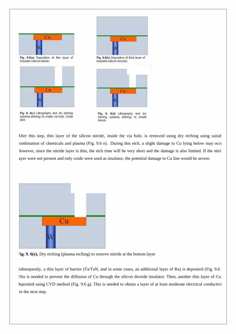
68
After this step, thin layer of the silicon nitride, inside the via hole, is removed using dry etching using suitable
combination of chemicals and plasma (Fig. 9.6 e). During this etch, a slight damage to Cu lying below may occur.
However, since the nitride layer is thin, the etch time will be very short and the damage is also limited. If the nitride
layer were not present and only oxide were used as insulator, the potential damage to Cu line would be severe.
Fig. 9. 6(e), Dry etching (plasma etching) to remove nitride at the bottom layer
Subsequently, a thin layer of barrier (Ta/TaN, and in some cases, an additional layer of Ru) is deposited (Fig. 9.6 f).
This is needed to prevent the diffusion of Cu through the silicon dioxide insulator. Then, another thin layer of Cu is
deposited using CVD method (Fig. 9.6 g). This is needed to obtain a layer of at least moderate electrical conductivity
for the next step.

69
Fig. 9.6(f), Ta/TaN deposition by PVD
Fig. 9. 6(g) Cu seed layer deposition by CVD (or PVD)
After the seed layer is deposited, a thick Cu layer is deposited using electrochemical deposition (Fig 9.6 h). The Cu
formed has larger crystals, lower electrical resistance and higher electromigration resistance compared to Cu deposited
by other methods such as PVD or CVD. The Cu can not be deposited only inside the vias and trenches. Hence it is
deposited throughout the wafer surface. Then in the next step, the excess Cu is removed using CMP (Fig. 9. 6 i)
Fig. 9. 6(h) Cu deposition by electrochemical deposition

70
Fig. 9. 6(i) Removal of excess Cu by first stage of CMP- (Main Cu CMP)
Fig. 9. 6(j) Ta/TaN (barrier layer) removal by 2nd stage of CMP (Barrier CMP)
The removal is done in two steps. In the first step, only the Cu is removed. The barrier and the insulator are not
removed (Fig. 9.6 i). In the second step or 2nd stage of the CMP, a different slurry is used and the barrier metal is also
removed in the unwanted places (Fig. 9.6 j). Subsequently, the Cu is annealed so that the crystal size increases.
This scheme of intergration is called “via first” integration because via holes are made before trenches here. In another
process sequence, the trenches can be made first and the vias can be made afterwards (i.e. the processes in Fig. 9.6 c
and Fig. 9.6 d can be done in reverse order) and that scheme is called “trench first” integration. Most fabs use the via
first scheme for copper metallization.
Summary: Process integration denotes combining various processes to obtain the desired structure, to obtain a
functioning chip, in a robust fashion. In the modern chips, the BEOL part plays a significant role in determining the
yield as well as the speed of the chip. Electromigration is the movement of metal atoms due to the movement of
electrons. It can cause failures at the later stage of chip operation and hence is a reliability issue. If the metal lines are
long, and/ or if large current densities are used, then the chances of failure by electromigration is high. It is desirable to
have high electromigration resistance and low electrical resistance. Aluminum has more electrical resistance than Cu
and less electromigration resistance than Cu. However, it can be etching using plasma and a process sequence using
tungsten vias and aluminum metal lines was used to make interconnects. With the introduction of CMP, it is possible
to make Cu vias and Cu metal lines on chips, and the different process sequence needed to obtain Cu interconnects
was discussed.

71
.UNIT-IV
GATE LEVEL DESIGN

72
Introduction
The module (integrated circuit) is implemented in terms of logic gates and interconnections between these
gates. Designer should know the gate-level diagram of the design. In general, gate-level modeling is used for
implementing lowest level modules in a design like, full-adder, multiplexers, etc.
Boolean algebra is used to represent logical(combinational logic) functions of digital circuits. A combinational
logic expression is a mathematical formula which is to be interpreted using the laws of Boolean algebra. Now
the goal of logic design or optimization is to find a network of logic gates that together compute the
combinational logic function we want.
For example, given the expression a+b , we can compute its truth value for any given values of a and b , and
also we can evaluate relationships such as a+b = c. but logic design is difficult for many reasons:
• We may not have a logic gate for every possible function, or even for every function of n inputs.
• Not all gate networks that compute a given function are alike-networks may differ greatly in their area and
speed.
• Thus combinational logic expressions are the specification,
• A logic gate is an idealized or physical device implementing a Boolean function, that is, it performs a logical
operation on one or more logic inputs and produces a single logic output.
• Logic gates are primarily implemented using diodes or transistors acting as electronic switches, but can also
be constructed using electromagnetic relays (relay logic), fluidic logic, pneumatic logic, optics, molecules, or
even mechanical elements.
• With amplification, logic gates can be cascaded in the same way that Boolean functions can be composed,
allowing the construction of a physical model of all of Boolean logic.
• simplest form of electronic logic is diode logic. This allows AND and OR gates to be built, but not inverters,
and so is an incomplete form of logic. Further, without some kind of amplification it is not possible to have
such basic logic operations cascaded as required for more complex logic functions.
• To build a functionally complete logic system, relays, valves (vacuum tubes), or transistors can be used.
• The simplest family of logic gates using bipolar transistors is called resistor-transistor logic (RTL). Unlike
diode logic gates, RTL gates can be cascaded indefinitely to produce more complex logic functions. These
gates were used in early integrated circuits. For higher speed, the resistors used in RTL were replaced by
diodes, leading to diode-transistor logic (DTL).
• Transistor-transistor logic (TTL) then supplanted DTL with the observation that one transistor could do the
job of two diodes even more quickly, using only half the space.
• In virtually every type of contemporary chip implementation of digital systems, the bipolar transistors have
been replaced by complementary field-effect transistors (MOSFETs) to reduce size and power consumption
still further, thereby resulting in complementary metal–oxide–semiconductor (CMOS) logic. that can be
described with Boolean logic.

73
cMOS logic gates and other complex gates
General logic circuit Any Boolean logic function (F) has two possible values, either logic 0 or logic 1. For
some of the input combinations, F = 1 and for all other input combinations, F = 0. So in general, any Boolean
logic function can be realized using a structure as shown in figure.
• The switch S1 is closed and switch S2 is open for input combinations that produces F = 1.
• The switch S1 is open and switch S2 is closed for input combinations that produces F = 1.
• The switch S1 is open and switch S2 is open for input combinations that produces F = 0.
Thus the output (F) is either connected to VDD or the ground, where the logic 0 is represented by the ground
and the logic 1 is represented by VDD. So the requirement of digital logic design is to implement the pull-up
switch(S1) and the pull-down switch(S2).
CMOS static logic
A generalized CMOS logic circuit consists of two transistor nets nMOS and pMOS. The pMOS transistor net
is connected between the power supply and the logic gate output called as pull-up network , Whereas the
nMOS transistor net is connected between the output and ground called as pull-down network. Depending on
the applied input logic, the PUN connects the output node to VDD and PDN connects the output node to the
ground.
The transistor network is related to the Boolean function with a straight forward design procedure:
• Design the pull down network (PDN) by realizing, AND(product) terms using series-connected nMOSFETs.
OR (sum) terms using parallel-connected nMOSFETS.
• Design the pull-up network by realizing,AND(product) terms using parallel-connected nMOSFETs. OR
(sum) terms using series-connected nMOSFETS.
• Add an inverter to the output to complement the function. Some functions are inherently negated, such as
NAND,NOR gates do not need an inverter at the output terminal.

74
CMOS inverter
A CMOS inverter is the simplest logic circuit that uses one nMOS and one pMOS transistor. The nMOS is
used in PDN and the pMOS is used in the PUN as shown in figure.
Working operation
1) When the input Vin is logic HIGH, then the nMOS transistor is ON and the pMOS transistor is OFF.
Thus the output Y is pulled down to ground (logic 0) since it is connected to ground but not to source VDD.
2) When the input Vin is logic LOW, then nMOS transistor is OFF and the pMOS transistor is ON, Thus
the output Y is pulled up to VDD(logic 1) since it is connected to source via pMOS but not to ground.
CMOS NAND gate
The two input NAND function is expressed by Y=A.B
Step 1 Take complement of Y
Y= A.B = A.B
Step 2 Design the PDN In this case, there is only one AND term, so there will be two nMOSFETs in series as
shown in figure.
Step 3 Design the PUN. In PUN there will be two pMOSFETs in parallel , as shown in figure

75
inally join the PUN and PDN as shown in figure which realizes two –input NAND gate. Note that we have
realized y, rather tat Y because the inversion is automatically provided by the nature of the CMOS circuit
operation,
Working operation
1) Whenever at least one of the inputs is LOW, the corresponding pMOS transistor will conduct while
the corresponding nMOS transistor will turn OFF. Subsequently, the output voltage will be HIGH.
2) Conversely, if both inputs are simultaneously HIGH, then both pMOS transistors will turn OFF, and
the output voltage will be pulled LOW by the two conducting nMOS transistors.
CMOS NOR gate
The two input NOR function is expressed by Y=A+B
Step 1 Take complement of Y,Y= A+B = A+B
Step 2 Design the PDN In this case, there is only one OR term, so there will be two nMOSFETs connected in
parallel, as shown in figure.
Step 3 Design the PUNIn PUN there will be two pMOSFETs in series , as shown in figure
Finally join the PUN and PDN as shown in figure which realizes two –input NAND gate. Note that we have
realized y, rather tat Y because the inversion is automatically provided by the nature of the cMOS circuit
operation,
Working operation
1) Whenever at least one of the inputs is LOW, the corresponding pMOS transistor will conduct while the
corresponding nMOS transistor will turn OFF. Subsequently, the output voltage will be HIGH.
2) Conversely, if both inputs are simultaneously HIGH, then both pMOS transistors will turn OFF, and the
output voltage will be pulled LOW by the two conducting nMOS transistors.

76
Complex gates in CMOS logic
A complex logic gate is one that implements a function that can provide the basic NOT, AND and OR
operation but integrates them into a single circuit. CMOS is ideally suited for creating gates that have logic
equations by exhibiting the following,
An AOI logic equation is equivalent to a complemented SOP from, while an AOI equation is equivalent to a
complemented POS structure. In CMOS, output always produces NOT operation acting on input variable.
1) AOI Logic Function (OR) Design of XOR gate using CMOS logic.
AND-OR-INVERT logic function(AOI) implements operation in the order AND,OR,NOT. For example ,
let us consider the function Y = AB+CD i.e., Y = NOT((A AND B)OR (C AND D)) The AOI logic gate
implementation for Y
CMOS implementation for Y
Step 1: Draw A.B (AND) function first by connecting 2 nMOS transistors in series.

77
2: Draw C.D implementation, by using 2 nMOS transistors in series.
Step 3: Y = A.B+C.D , In this function A.B and C.D are added, for addition , we have to draw parallel
connection. So, A.B series connected in parallel with C.D as shown in figure.
Step 4: Draw pMOS connection,
In nMOS A,B connected in series. So, in pMOS side, A.B should be connected in parallel.
In nMOS C,D connected in series. So, in pMOS side, C.D should be connected in parallel.
A.B and C.D networks are connected in parallel in nMOS side. So, in pMOS side, A.B and C.D networks
should be connected in series.
In pMOS multiplication should be drawn in parallel, then addition should be drawn in series as shown in
figure.
Step 5: Take output at the point in between nMOS and pMOS networks.

78
1) OAI Logic Function (OR) Design of XNOR gate using CMOS logic.
OR-AND-INVERT logic function(AOI) implements operation in the order OR,AND,NOT. For example ,let
us consider the function Y = (A+B).(C+D) i.e., Y = NOT((A OR B)AND (C OR D))
The OAI logic gate implementation for Y

79
MOS implementation for Y
SWITCH LOGIC
1) Switch logic is mainly based on pass transistor or transmission gate.
2) It is fast for small arrays and takes no static current from the supply, VDD. Hence power
dissipation of such arrays is small since current only flows on switching.
3) Switch (pass transistor) logic is analogous to logic arrays based on relay contacts, where in path
through each switch is isolated from the logic levels activating the switch.
PASS TRANSISTOR
1) This logic uses transistors as switches to carry logic signals from node to node instead of
connectiong output nodes directly to VDD or ground(GND)
2) If a single transistor is a switch between two nodes, then voltage degradation.equal to vt
(threshold voltage) for high or low level depends up on nMOS or pMOS logic.
3) When using nMOS switch logic no pass transistor gate input may be driven through one or more
pass transistors as shown in figure.

80
4) Since the signal out of pass transistor T1 does not reach a full logic 1 by threshold voltage effects
signal is degraded by below a tru e logic 1, this degraged voltage would not permit the output of T2 to reach an
acceptable logic 1 level.
Advantages
They have topological simplicity.
1) Requires minimum geometry.
2) Do not dissipate standby power, since they do not have a path from supply to ground.
Disadvantages
1) Degradation in the voltage levels due to undesirable threshold voltage effects.
2) Never drive a pass transistor with the output of another pass transistor.
TRANSMISSION GATE
1) It is an electronic element, good non-mechanical relay built with CMOS technology.
2) It is made by parallel combination of an nMOS and pMOS transistors with the input at gate of one
transistor being complementary to the input at the gate of the other as shown in figure.
3) Thus current can flow through this element in either direction.
4) Depending on whether or not there is a voltage on the gate, the connection between
the input and output is either low resistance or high-resistance, respectively Ron = 100Ω and Roff > 5 MΩ.
Operation
• When the gate input to the nMOS transistor is ‘0’ and the complementary ‘1’ is gate input to the pMOS ,
thus both are turned off.
• When gate input to the nMOS is ‘1’ and its complementary ‘0’ is the gate input to the pMOS , both are
turned on and passes any signal ‘1’ and ‘0’ equally without any degradation.
• The use of transmission gates eliminates the undesirable threshold voltage effects which give rise to loss of
logic levels in pass-transistors as shown in figure.
Advantages
1) Transmission gates eliminates the signal degradation in the output logic levels.
2) Transmission gate consists of two transistors in parallel and except near the positive and negative rails.

81
Disadvantages
1) Transmission gate requires more area than nMOS pass circuitry.
2) Transmission gate requires complemented control signals.
“ Transmission gate logic can be used to design multiplexers(selector functions)”.
Design a 2-input multiplexer using CMOS transmission gates.
Figure shows a 2-input multiplexer circuit using CMOS transmission gate.
If the control input S is low, the TG0 conducts and the output F is equal to A. On the other hand, if the control
input S is high the TG1 conducts and the output F is equal to B.
ALTERNATIVE GATE CIRCUITS
CMOS suffers from increased area and correspondingly increased capacitance and delay, as the logic gates
become more complex. For this reason, designers developed circuits (Alternate gate circuits) that can be used
to supplement the complementary type circuits . These forms are not intended to replace CMOS but rather to
be used in special applications for special purposes.
PSEUDO nMOS Logic
Pseudo nMOS logic is one type of alternate gate circuit that is used as a supplement for the complementary
MOS logic circuits. In the pseudo-nMOS logic, the pull up network (PUN) is realized by a single pMOS
transistor. The gate terminal of the pMOS transistor is connected to the ground. It remains permanently in the
ON state. Depending on the input combinations, output goes low through the PDN. Figure shows the general
building block of logic circuits that follows pseudo nMOS logic.
Here, only the nMOS logic (Qn) is driven by the input voltage, while the gate of p-transistor(Qp) is connected

82
to ground or substrate and Qp acts as an active load for Qn. Except for the load device, the pseudo-nMOS gate
circuit is identical to the pull-down network(PDN) of the complementary CMOS gate.
The realization of logic circuits using pseudo-nMOS logic is as shown in figure.
Advantages
1) Uses less number of transistors as compared to CMOS logic.
2) Geometrical area and delay gets reduced as it requires less transistors.
3) Low power dissipation.
Disadvantages
1) The main drawback of using a pseudo nMOS gate instead of a CMOS gate is that the always on
PMOS load conducts a steady current when the output voltage is lower than VDD.
2) Layout problems are critical.
DYNAMIC CMOS LOGIC
A dynamic CMOS logic uses charge storage and clocking properties of MOS transistors to implement logic
operations. Figure shows the basic building block of dynamic CMOS logic. Here the global clock ø drives
nMOS evaluation transistor and pMOS precharge transistor. A logic is implemented using an nFET array
connected between output node and ground.

83
The gate (clock ø) defines two phases, evaluation and precharge phase during each clock cycle.
Working
• When clock ø = 0 the circuit is in precharge phase with the pMOS device Mp ON and the evaluation
nMOS Mn OFF. This establishes a conducting path between VDD and the output allowing Cout to charge to a
voltage Vout = VDD. Mp is often called the precharge FET.
• When clock ø = 1 the circuit is in evaluation phase with the pMOS device Mp OFF and the
evaluation nMOS Mn ON. If the logic block acts like a closed switch the Cout can discharge through logic
array and Mn, this gives a final result of Vout = VDD, logically this is an output of F = 1. Charge leakage
eventually drops the output to Vout = 0 Vwhich could be an incorrect logic value.
The logic formation is formed by three series connected FETs (3-input NAND gate) is shown in figure.
The dynamic CMOS logic circuit has a serious problem when they are cascaded. In the precharged phase (ø =
0) , output of all the stages are pre-charged to logic high. In the evaluation phase (ø = 1), the output of all
stages are evaluated simultaneously. Suppose in the first stage, the inputs are such that the output is logic low
after the evaluation. In the second stage, the output of the first stage is one input and there are other inputs. If
theouther inputs of the second stage are such that output of it discharges to logic low, then the evaluated output
of the first stage can never make the output of the second stage logic high. Ths is because, by the time the first
stage is being evaluated, output of the second. Stage is discharged, since evaluation happens simultaneously.
Remember that the output cannot be charged to logic high in the evaluation phase (ø = 1, pMOSFET in PUN
is OFF), it can only be retained in the logic high depending on the inputs.
Advantages
1) Low power dissipation.
2) Large noise margin.
3) Small area due to less number of transistors.\

84
CMOS DOMINO LOGIC
Standard CMOS logic gates need a PMOS and an NMOS transistor for each logic input. The pMOS transistors
require a greater area tan the nMOS transistors carrying the same current. So, a large chip area is necessary to
perform complex logic operations. The package density in CMOS is improved if a dynamic logic circuit,
called the domino CMOS logic circuit, is used.
Domino CMOS logic is slightly modified version of the dynamic CMOS logic circuit. In this case, a static
inverter is connected at the output of each dynamic CMOS logic block. The addition of the inverter solves the
problem of cascading of dynamic CMOS logic circuits.
The circuit diagram of domino CMOS logic structures as shown in figure as follows
A domino CMOS AND-OR gate that realizes the function y = AB + CD is depicted in fugure .
The left hand part of the circuit containing Mn,Mp, T1,T2,,T3,and T4 forms and AND-OR-
INVERTER (AOI) gate. It derives the static CMOS inverter formed by N2 and P2 in the right-
hand part of the circuit. The domino gate is activated by the single phase clock ø applied to the NMOS (Mn)
and the PMOS (Mp) transistors. The load on the AOI part of the circuits is the parasitic load capacitance.
Working
• When ø = 0, is ON and Mn is OFF, so that no current flows in the AND-OR paths of the AOI. The
capacitor CL is charged to VDD through Mp since the latter is ON. The input to the inverter is high, and drives
the output voltage V0 to logic-0.
• When ø = 1, Mp is turned OFF and Mn is turned ON. If either (or both) A and B or C and D is at
logic-1, CL discharges through either T2,T1 and Mn or T3,T4 and Mp. So , the inverter input is driven to logic-
0 and hence the output voltage V0 to logic-1. The Boolean expression for the output voltage is Y = AB + CD.
Note : Logic input can change only when ø = 0. No changes of the inputs are permitted when ø = 1 since a
discharge path may occur.

85
Advantages
1) Smaller areas compared to conventional CMOS logic.
2) Parasitic capacitances are smaller so that higher operating speeds are possible.
3) Operation is free of glitches since each gate can make one transition.
disadvantages
1) Non inverting structures are possible because of the presence of inverting buffer.
2) Charge distribution may be a problem.
CLOCKED CMOS LOGIC
The clocked CMOS logic is also referred as C2MOS logic. Figure shows the general arrangement of a clocked
CMOS (C2MOS) logic. A pull-up p-block and a complementary n-block pull-down structure represent p and
n-transistors respectively and are used as implement clocked CMOS logic shown in figure. However, the logic
in this case is connected to the output only during the ON period of the clock. Figure shows a clocked inverter
circuit which is also belongs to clocked CMOS logic family. The slower rise times and fall times can be
expected due to owing of extra transistors in series with the output.
Working
• When ø = 1 the circuit acts an inverter , because transistors Q3 and Q4 are ‘ON’ . It is said to be in the
“evaluation mode”. Therefore the output Z changes its previous value.
• When ø = 0 the circuit is in hold mode, because transistors Q3 and Q4 becomes ‘OFF’ . It is said to be in the
“precharge mode”. Therefore the output Z remains its previous value.
n-p CMOS LOGIC
Figure shows the another variation of basic dynamic logic arrangement of CMOS logic called as n-p CMOS
logic. In this, logic the actual logic blocks are alternatively ‘n’ and ‘p’ in a cascaded structure. The clock ø and
ø- are used alternatively to fed the precharge and evaluate transistors. However, the functions of top and
bottom transistors are also alternate between precharge and evaluate transistors.

86
Working
• During the pre charge phase ø = 0 , the output of the n-tree gate, OUT 1 OUT3 , are charged to VDD, while
the output of the p-tree gate OUT2 is pre discharged to 0V. Since the n-tree gate connects pMOS pull-up
devices, the PUN of the p-tree is turned off at that time.
• During the evaluation phase ø = 1, the outputs (OUT1,OUT3) of the n-tree gate can only make a 1- 0
transition, conditionally turning on some transistors in the p-tree. This ensures that no accidental discharge of
OUT 2 can occur.
• Similarly n-tree blocks can follow p-tree gates without any problems, because the inputs to the n-gate are pre
charged to 0.
Disadvantages
Here, the p-tree blocks are slower than the n-tree modules, due to the lower current drive of the pMOS
transistors in the logic network.
BASIC CIRCUIT CONCEPTS
In VLSI design the wiring up (interconnection) of circuits takes place through the various conductive layers
which are produced by the MOS processing. So, it is necessary to know the resistive and capacitive
characteristics of each layer. Concepts such as
• resistance RS and a standard unit of capacitance cg which helps in evaluating the effects of wiring
and input and output capacitances.
• The delays associated with wiring with inverters and with other circuitry evaluated interms of a delay
unit τ.
Sheet Resistance RS
• The sheet resistance is a measure of resistance of thin films that have a uniform thickness.
• It is commonly used to characterize materials made by semiconductor doping, metal deposition,
resistive paste printing and glass coating.
Ex: doped semiconductor regions (silicon or polysilicon ) and resistors.
• Sheet resistance is applicable to two-dimensional systems where the thin film is considered to be a
two- dimensional entity.
Consider a uniform slab of conducting material of resistivity ρ of width W, thickness t and length between
faces A&B is L. as shown in figure.
Consider the resistance RAB between two opposite faces
Where A is area of cross section

87
Consider a case in which L = W . It means square of resistive material
Where RS is ohm per square or sheet resistance.
From the above equation RS is independent of the area of square., for example a 1µm per side square slab of
the material has same resistance as 1 cm per side square slab of the same material if the thickness is same.
Hence, the resistance of the MOS layers depend on the thickness and the resistivity of the material of the layer.
• The thickness of the metal and polysilicon deposited is known by measuring using four probe method.
• The resistivity of the diffusion layers is measured by measuring the penetration depth of the diffusion regions.
Sheet resistance concept applied to MOS Transistors and Inverterts:
Consider the transistor structures by distinguish the actual diffusion (active) regions from the channel regions.
The simple n-type pass transistor has a channel length L = 2λ and a channel width W=2λ.
Hence the channel is square and the channel resistance is
Here the length to width ratio denotes the impedance (Z) and is equal to 1:1. Consider another transistor has a
channel length L = 8λ and width W = 2λ.

88
Thus, channel resistance
Typical sheet resistances of MOS layers are tabulated
Layer RS ohm per square
5µm Orbit Orbit 1.2µm
Metal 0.03 0.04 0.04
Diffusion 15 - 100 20 - 45 20 - 45
Silicide 2 - 4 --- ---
Polysilicon 15 - 100 15 - 30 15 - 30
n- channel 104 2 X 10
4 2 X 10
4
p-channel 2.5 X 10⁴ 4.5 X 10
4 4.5 X 10
4
Sheet resistance for Inverters
Consider an nMOS inverter has the channel length 8λ and width 2λ for pull up transistor as shown in figure.
L = 8λ; W = 2λ
Z = L/W = 4
Sheet resistance R = Z.RS = 4 X 104 = 40 KΩ
For pull down transistor the channel length 2λ and width 2λ, then the sheet resistance is
R = Z.RS = 1 X 104 = 10 KΩ
Hence Zp.u to Zp.d = 4:1 hence the ON resistance between VDD and VSS is the total series resistance i.e.,
RON = 40 KΩ + 10 KΩ = 50 KΩ
Consider the simple CMOS inverter as shown in figure.

89
Here the pull up transistor is of p-type device with channel length 2λ and width 2λ.
Z = L/W =1
Then Sheet resistance RSP = Z.RS = 1 X 2.5 X 104 = 25 KΩ
The pull down transistor is of n-type with channel length 2λ and width 2λ.
Z = L/W =1
Hence, Sheet resistance RSN = Z.RS = 1 X 104 = 10 KΩ.
In this case, there is no static resistance between VDD and VSS . Since at any point of time only one transistor is
ON, but not both.
When Vin = 1, the ON resistance is 10KΩ Vin = 0, the ON resistance is 25KΩ
Area capacitance of layers
From the concept of the transistors, it is apparent that as gate is separated from the channel by gate oxide an
insulating layer, it has capacitance. Similarly different interconnects run on the chip and each layer is
separated by silicon dioxide .
For any layer by knowing the dielectric thickness, we can calculate the area capacitance as follows
Where, A is area of the plates , D is the thickness of Sio2, Є0 is the permittivity of the free space
and Єins is the relative permittivity of insulator(Sio2).

90
Typical area capacitance values of MOS circuits
Layer Value in pF X 10-4
/ µm2 (Relative values in brackets )
5µm Orbit Orbit 1.2µm
Gate to channel 4 (1.0) 8 (1.0) 16 (1.0)
Diffusion 1 (0.25) 1.75 (0.22) 3.75 (0.23)
Polysilicon to substrate 0.4 (0.1) 0.6 (0.075) 0.6 (0.038)
Metal 1 to substrate 0.3 (0.075) 0.33 (0.04) 0.33 (0.02)
Metal 2 to substrate 0.2 (0.05) 0.17 (0.02) 0.17 (0.01)
Metal 2 to metal 1 0.4 (0.1) 0.5 (0.06) 0.5 (0.03)
Metal 1 to poly silicon 0.3(0.075) 0.3 (0.038) 0.3 (0.018)
Standard unit of capacitance cg
It is defined as the gate – to – channel capacitance of a MOS transistor having W = L . i.e., standard square as
shown in figure. The unit is denoted by cg. cg may be calculated for any MOS process as follows
For 5µm MOS circuits
Area/standard square = 5µm X 5µm = 25 µm2
Capacitance value = 4 X 10⁻⁴
pF/ µm2

Thus, standard value cg = 25 µm2 X 4 X 10
-4 pF/ µm
2 = 0.01 pF
For 2µm MOS circuits
Area/standard square = 2µm X 2µm = 4 µm2
Capacitance value = 8 X 10⁻⁴
pF/ µm2
Thus, standard value cg = 4 µm2 X 8 X 10
-4 pF/ µm
2 = 0.01 pF
For 1.2µm MOS circuits
Area/standard square = 1.2µm X 1.2µm = 1.44 µm2
Capacitance value = 16 X 10-4
pF/ µm2
Thus, standard value cg = 1.44 µm2 X 16 X 10
-4 pF/ µm
2 = 0.0023 pF
Calculation for capacitance value
The calculation of capacitance value is established by the ration between the area of interest and the area of
standard gate and multiplying this ration by the appropriate relative C value from tabular form. The product will
give the required capacitance in cg units.
Consider the area defined as shown in figure of length 20λ and width 3λ
Area relative to the standard gate
Relative area = Area( L X W )/standard gate area
= 15 .
1) consider the area in metal 1
capacitance to substrate = relative area X relative C value (from table)
= 15 X 0.075 cg
= 1.125 cg
2) consider the same area in polysilicon capacitance to substrate = 15 X 0.1cg
= 1.5 cg
3) consider the same area in n- type diffusion capacitance to substrate = 15 X 0.25cg
= =3.75 cg
Consider the following structure which occupies more than one layer as shown in figure and calculate the area
capacitance value

while calculating the area value in the above figure neglect the contact region where the metal is connected to
polysilicon and shielded from the substrate.
( i)consider the metal area
Relative area = Area( L X W )/standard gate area
= 75
metal capacitance = relative area X relative C value (from table)
= 75 X 0.075 cg
= 5.625 cg
3) consider the polysilicon area (excluding the gate region) capacitance to substrate = 15 0.1cg
= 1.5 cg
3) consider the same area in n- type diffusion capacitance to substrate = 15 X 0.25cg
= 3.75
We know that the transit time (τsd) from source to drain
Here the Vds varies as Cg charges from 0 volts to 63% of Vdd in period τ. Thus the average value of Vds = 3V.
For 5µm technology
τsd = 0.13 n sec, τsd τ
Similarly the transition point of an inverter or gate is 0.5 VDD which is approximately equal to 0.63 VDD (time

constant). From this we can conclude that we can use the transit time and time constant interchangeably and ‘stray’
capacitances are allowed for doubling the theoretical values calculated.
Thus, τ is used as the fundamental time unit and all timings in a system can be assessed in relation to τ ,Hence for
5µm MOS technology τ = 0.3 nsec.
for 2µm MOS technology τ = 0.2 nsec.
for 1.2µm MOS technology τ = 0.1 nsec.
INVERTER DELAYS
Consider the basic nMOS inverter has the channel length 8λ and width 2λ for pull-up transistor and channel length
of 2λ and width 2λ for pull down transistor.
Hence the sheet resistance for pull-up transistor is Rp.u = 4RS = 40kΩ and
sheet resistance for pull-up transistor is Rp.d = 1RS = 10kΩ.
Since (τ = RC) depends upon the values of R & C, the delay associates with the inverter depend up on whether it is
being turned on (or ) off. Now, consider a pair of cascaded inverters as shown in figure, then the delay over the pair
will be constant irrespective of the sense of the logic level transition of the input to the first .
In general, the delay through a pair of similar nMOS inverters is Td = (1 + Zp.u/Zp.d ) τ
Assume that τ = 0.3 n sec.
Then ,Td = (1 + 4) 0.3
= 5 τ
Thus, the inverter pair delay for inverters having 4:1 ration is 5τ.
Hence, a single 4:1 inverter exhibits undesirable asymmetric delays, Since the delay in turning ON is τ and delay in
turning OFF is 4τ.
CMOS inverter pair delay
When we consider CMOS inverters, the rules for nMOS inverters are not applicable. But we need to consider the
natural (RS) uneven values for equal size pull up p-transistor and the n-type pull down transistors.

Figure shows the theoretical delay associated with a pair of both n and p transistors lambda based inverters. Here
the gate capacitance is double comparable to nMOS inverter since the input to a CMOS inverter is connected to
both transistor gate. NOTE: Here the asymmetry (uneven) of resistance
values can be eliminated by increasing the width of the p-device channel by a factor of two or three at the same
time the gate capacitance of p-transistor also increased by the same factor.
Formal estimation of CMOS inverter delay
In CMOS inverter by the charging and discharging of a capacitive load CL , we can estimate the Rise time and fall
time from the following simple analysis.
Rise time estimation
In this analysis we assume that the p-device stays in saturation for the entire charging period of the load capacitor
CL.
Consider the circuit as follows
Saturation current for the p-transistor is given by
This current charges CL and since its magnitude is approximately constant, we have
Substitute the value of Idsp in above equation and then the rise time is
Assume that t = τr when Vout = VDD then

If Vtp = 0.2VDD, then
Fall time estimation
Consider the circuit for discharge of CL through n-transistor as follows
By making similar assumptions we can write for fall-time estimation,
From the above two estimations we can deduce that
We know that
and hence
So that the rise time is slower by a factor of 2.5 when using minimum size devices for both n & p.
• In order to achieve symmetrical operation using minimum channel length we need to make Wp = 2.5 Wn.
• For minimum size lambda based geometries this would result in the inverter having an input
capacitance of
1cg (n-device) + 2.5cg(p-device) = 3.5cg
From the above equations we can conclude that
1. τr and τf are proportional to 1/VDD
2. τr and τf are proportional to CL
3. τr = 2.5τf for equal n and p- transistor geometries.
Driving Large capacitive loads

when signals are propagated from the chip to off chip destinations we can face problems to drive large capacitive
loads. Generally off chip capacitances may be several orders higher than on chip cg values.
CL ≥ 104 cg
Where CL denotes offchip load. The capacitances which of this order must be driven through low resistances,
otherwise excessively long delays will occur. Large capacitance is presented at the input, which in turn slows down
the rate of change of voltage at input.
Cascaded Inverters as drivers
Inverters to drive large capacitive loads must be present low pull-up and pull down resistance. For MOS
circuits low resistance values imply low L:W ratio(since ) . Since length L cannot be reduced below the
minimum feature size, the channels must be made very wide to reduce resistance value. Consider N cascaded
inverters as on increasing the width factor of ‘f’ than the previous stage as shown in
figure.
As the width factor increases, the capacitive load presented at the inverter input increases and the area occupied
increases also. It is observed that as the width increases, the number N of stages are decreased to drive a particular
value of CL. Thus with large f(width), N decreases but delay per stage increases for 4:1 nMOS inverters.
Delay per stage = fτ for ∆Vin
=4fτ for ∆-Vin
Where ∆Vin indicates logic 0 to 1 transition and
∆-Vin indicates logic 1 to 0 transition of Vin
Toal delay per nMOS pair = 4fτ
Similarly delay per CMOS pair = 7fτ.
Calculation for time delay
Let us assume y = CL/cg = f N
Determine the value of f which will minimize the overall delay for a given value of y. Apply logarithms on both
sides in the above equation
ln(y) = ln(f N)
ln (y) = N ln (f)
N= ln(y)/ln(f)
For N even
Total delay = N/2 5fτ
= 2.5 Nfτ (nMOS)
(Or) toal delay = N/2 7fτ
= 3.5Nfτ (CMOS)
From above relations, we can write

Delay α Nfτ
= ln(y)/ln(f) . fτ
It can be shown that total delay is minimized if f assumes the value of e for both CMOS and nMOS inverters.
Assume f = e N = ln(y)/ln(e)
N = ln(y)
Overall delay td N even td = 2.5 eNτ (nMOS)
(or) td = 3.5 eNτ(CMOS)
Î N odd td = [2.5(N-1) +1] eτ (nMOS)
td = [3.5(N-1) +2] eτ (CMOS) ( for logical transition 0 to 1)
( or) td = [ 2.5(N-1) + 4] eτ (nMOS)
td = [3.5(N-1) +5] eτ (CMOS) (for logical transition 1 to 0)
Super buffers
Generally the pull-up and the pull down transistors are not equally capable to drive capacitive loads. This
asymmetry is avoided in super buffers. Basically, a super buffer is a symmetric inverting or non inverting driver
that can supply (or) remove large currents and is nearly symmetrical in its ability to drive capacitive load. It can
switch large capacitive loads than an inverter. An inverting type nMOS super buffer as shown in figure.
• Consider a positive going (0 to 1) transition at input Vin turns ON the inverter formed by T1 and T2.
• With a small delay, the gate of T3 is pulled down to 0 volts. Thus, device T3 is cut off. Since gate of T4 is
connected to Vin, it is turned ON and the output is pulled down very fast.
For the opposite transition of Vin (1 to 0), Vin drops to 0 volts. The gate of transistor T3 is allowed to rise to VDD
quickly.
• Simultaneously the low Vin turns off T4 very fast. This makes T3 to conduct with its gate voltage approximately
equal to VDD.
• This gate voltage is twice the average voltage that would appear if the gate was connected to the source as in the
conventional nMOS inverter.
Now as Idsα Vgs , doubling the effective Vgs increases the current and there by reduces the delay in charging at the
load capacitor of the output. The result is more symmetrical transition.

Figure shows the non-inverting nMOS super buffer where the structures fabricated in 5µm technology are capable
of driving capacitance of 2pF with a rise time of 5nsec.
BiCMOS drivers
1. In BiCMOS technology we use bipolar transistor drivers as the output stage of inverter and logic gate circuits.
2. In bipolar transistors, there is an exponential dependence of the collector (output) current on the base to emitter
(input) voltage Vbe .
3. Hence, the bipolar transistors can be operated with much smaller input voltage swings than MOS transistors and
still switch large current.
4. Another consideration in bipolar devices is that the temperature effect on input voltage Vbe.
5. In bipolar transistor, Vbe is logarithmically dependent on collector current IC and also other parameters such as
base width, doping level, electron mobility.
6. Now, the temperature differences across an IC are not very high. Thus the Vbe values of the bipolar devices
spread over the chip remain same and do not differ by more than a few milli volts.
The switching performance of a bipolar transistor driving a capacitive load can be analyzed to begin with the help
of equivalent circuit as shown in figure.
The time ∆t required to change the output voltage Vout by an amount equal to the input voltage is
∆t = CL/gm
Where,
CL is the load capacitance
gm is the trans conductance of the bipolar transistor.
The value of ∆t is small because the trans conductance of the bipolar transistors is relatively high.
There are two main components which reveals the delay due to the bipolar transistors are Tin and TL .
• Tin is the time required to first charge the base emitter junction of the bipolar (npn) transistor. This time is
typically 2ns for the BiCMOS transistor base driver.
For the CMOS driver the time required to charge the input gate capacitance is 1ns.
• TL is the time required to charge the output load capacitance .
• The combined effect of Tin and TL is represented as shown in figure.

• Delay of BiCMOS inverter can be described by
• Delay for BiCMOS inverter s reduced by a factor of hfe as compared with a CMOS inverter.
• In Bipolar transistors while considering delay another significant parameter is collector resistance Rc through
which the charging current for CL flows.
• For a high value of RC, there is a long propagation delay through the transistor when charging a capacitive load.
• Figure shows the typical delay values at two values of CL as follows.
The devices thus have high β, high gm, high hfe and low RC. The presence of such efficient and advantageous
devices on chip offers a great deal of scope and freedom to the VLSI designer.
Propagation delays
Propagation delay is the delay in the propagation of the signal created by the change of logical status at the input to
create same change at the output.
(i)Cascaded pass transistors
Figure shows a chain of four pass transistors driving a capacitive load CL. All the gates are supplied by VDD so that
a signal can propagate to the output. The lamped RC equivalent circuit is shown in figure, where each transistor is
modeled by a series resistance and capacitance representing the gate-to-channel capacitance and stray capacitances.
Them minimum value of R is the turned ON resistance of each enhancement mode pass transistor.

The current through the capacitance at the node with voltage V2 is
C (dV2 / dt ) ≈ C.∆V2/ ∆t
The current entering at this node is I1 = (V1 – V2)/R and the current leaving from this node is I2 = (V2 – V3)/R. By
applying KCL at this node
IC = I1 – I2
C . ∆V2/ ∆t = I1 – I2 = ((V1 – V2)- (V2 – V3)) / R
As the number of sections in the network increases, the circuit parameters become distributed.
Assume that R and C as the resistance per unit length and the capacitance per unit length respectively.
C∆* .∆V2/ ∆t = ∆(∆V2)/R.∆X
Where x is the distance along the network from the input.
RC dv/dt = d/dx. (dv/dx) = d2V/dx
2
The propagation time τp from a signal to propagate a distance x is
τp α X2
By simplifying the analysis if all sheet resistance, gate-to-channel capacitance RS and cg are lumped together
R total = nr Rs
C total = nccg
Where r gives relative resistance per section interms of RS and c gives relative capacitance per section interms of
cg . Then the overall delay for n sections is given by
τp = n2rc(τ)
It can be shown that the signal delay in a section containing N identical pass transistors driving a matched load (CL
= Cg) is τp = 0.7 * N(N+1)/2 *RCL
For large value of N, the quantity (N + 1) can be replaced by N. Since the delay increases with N, the number of
pass transistors is restricted to 4. A cascade of more pass transistors will produce a very slow circuit and the signal
needs to be restored by an inverter after every three (or) four pass transsitor.
Design of long polysilicon wires
Long polysilicon wires also contribute distributed series R and C as was the case for cascaded pass transistors and
inconsequence signal propagation is slowed down. This would also be the case for wires in diffusion where the
value of C may be quite high, and for this reason the designer is discouraged from running signals in diffusion
except over very short distances.
For long polysilicon runs, the use of buffers is recommended. In general, the use of buffers to drive long
polysilicon runs has two desirable effects. First, the signal propagation is speeded up and second there is a
reduction in sensitivity to noise. In the diagram the slow rise-time of the signal at the input of the inverter means
that the input voltage spends a relatively long time in the vicinity of Vinv so that small disturbances due to noise will
switch the inverter state between ‘0’ and’1’ as shown at the output point.

Thus , it is essential that long polysilicon wires be driven by suitable buffers to guard against the effects of noise
and to speed up the rise-time of propagated signal edges.
Wiring capacitances
The significant sources of capacitance which contribute to the overall wiring capacitance are as follows
(i)Fringing fields
Capacitance due to fringing field effects can be a major component of the overall capacitance of interconnect wires.
For fine line metallization, the value of fringing field capacitance (Cff) can be of the same order as that of the area
capacitance. Thus , Cff should be taken into account if accurate prediction of performance is needed.
Where l = wire length
t = thickness of wire
d = wire to substrate separation.
Then, total wire capacitance
Cw = Carea + Cff
(ii)Interlayer capacitances
From the definition of capacitance itself, it can be said that there exists a capacitance between the layers due to
parallel plate effects. This capacitance will depend upon the layout i.e., where the layers cross or whether one layer
underlies another etc., by the knowledge of these capacitances, the accuracy of circuit modeling and delay
calculations will be improved. It can be readily calculated for regular structures.
(iii) peripheral capacitance
1. The source and drain p-diffusion regions forms junctions with the n-substrate (or n-well) at well defined
and uniform depths.
2. Similarly, the source and drain n-diffusion regions forms junctions with p-substrate (or p-well) at well
defined and uniform depths.
3. Hence, for diffusion regions, each diode thus formed has associated a peripheral (side wall) capacitance
with it.
4. As a whole the peripheral capacitance,Cp will be the order of pF/unit length. So its value will be greater
than Carea of the diffusion region to substrate.
Cp increases with reduction in source or drain area.
Total diffusion capacitance is Cdiff = Carea + Cp
However, as the n and p-active regions are formed by impure implants at the surface of the silicon incase of orbit
processes, they have negligible depth. Hence Cp is quite negligible in them.
Typical values are given in tabular form

Diffusion capacitance Typical values
5µm 2µm 1.2µm
Area C (C area) 1.0 × 10⁻⁴
pF/µm2 1.75 × 10
-4pF/µm
2 3.75 × 10
-4pF/µm
2
Periphery (Cperiph) 8.0 × 10⁻⁴
pF/µm2 Negligible (assuming implanted negligible
regions of negligible depth)
Fan – in and Fan-out
Fan-in: The number of inputs to a gate is called as fan - in.
Fan-out: The maximum number of similar gates that a gate can drive while remaining within the guaranteed
specifications is called as fan-out.
Effects of Fan-in and Fan-out on propagation delay:
• An additional input to a CMOS logic gate requires an additional nMOS and pMOS i.e., two additional transistors,
while incase of other MOS logic gates, it requires one additional transistor.
• In CMOS logic gates, due to these additional transistors, not only the chip area but also the total effective
capacitance per gate also increased and hence propagation delay increases.
• Some of the increase in propagation delay time can be compensated by the size-scaling method.
• By increasing the size of the device, its current driving capability can be preserved.
• Due to increase in both of inputs and devices size, the capacitance increases, Hence propagation delay will still
increase with fan-in.
• An increase in the number of outputs of a logic gate directly adds to its load capacitances. Hence, the propagation
delay increases with fan-out.
Fan-In = Number of inputs to a logic gate
– 4 input NAND has a FI = 4
– 2 input NOR has a FI = 2, etc. (See Fig. a below.)
• Fan-Out (FO)= Number of gate inputs which are driven by a particular gate output
– FO = 4 in Fig. b below shows an output wire feeding an input on four different logic gates
• The circuit delay of a gate is a function of both the Fan-In and the Fan-Out.
Ex. m-input NAND: tdr = (Rp/n)(mnCd + Cr + kCg)
= tinternal-r + k toutput-r
• where n = width multiplier, m = fan-in, k = fan-out, Rp = resistance of min inverter P Tx, Cg = gate
capacitance, Cd = source/drain capacitance, Cr = routing (wiring) capacitance.

•
Choice of layers
The following are the constraints which must be considered for the proper choice of layers.
1. Since the polysilicon layer has relatively high specific resistance (RS), it should not be used for routing
VDD and VSS (GND) except for small distances.
2. VDD and GND (VSS) must be distributed only on metal layers, due to the consideration of Rs value.
3. The capacitive effects will also impose certain restrictions in the choice of layers as follows
(i) where fast signal lines are required, and in relation to signals on wiring which has relatively higher
values of RS.
(ii) The diffusion areas have higher values of capacitance to substrate and are harder to drive.
4. Over small equipotential regions, the signal on a wire can be treated as being identical at all points.
5. Within each region the propagation delay of the signal will comparably smaller than the gate delays and
signal delays caused in a system connected by wires.
Thus the wires in a MOS system can be modeled as simple capacitors. This concept leads to the establishment of
electrical rules (guidelines) for communication paths(wires) as given in tabular form.
Layer Maximum length of communication wire
Lambda based µm based (2µm) µm – based(1.2µm)
5µm
Metal Chip wide Chip wide Chip wide
Silicide 2,000λ NA NA
Polysilicon 200λ 400µm 250µm
Diffusion (active) 20λ 100µm 60µm


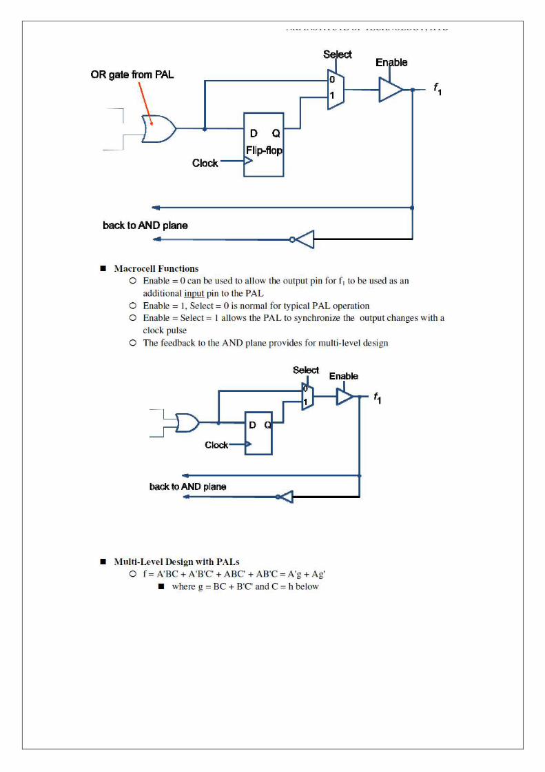


Unit V
Data Path Subsystems

5.1 Introduction
Most digital functions can be divided into the following categories:
1.Datapath operators 2.Memory elements 3.Control structures 4.Special-purpose cells
o I/O
o Power distribution
o Clock generation and distribution
o Analog and RF
CMOS system design consists of partitioning the system into subsystems of the types listed above.
Many options exist that make trade-offs between speed, density, programmability, ease of design,
and other variables. This chapter addresses design options for common datapath operators. The next
chapter addresses arrays, especially those used for memory. Control structures are most commonly
coded in a hardware description language and synthesized.
Datapath operators benefit from the structured design principles of hierarchy, regularity, modularity,
and locality. They may use N identical circuits to process N-bit data. Related data operators are
placed physically adjacent to each other to reduce wire length and delay. Generally, data is arranged
to flow in one direction, while control signals are introduced in a direction orthogonal to the
dataflow.
Common datapath operators considered in this chapter include adders, one/zero detectors,
comparators, counters, shifters, ALUs, and multipliers.
5.2 Shifters
Consider a direct MOS switch implementation of a 4X4 crossbar switch as shown in Fig. 5.1.
The arrangement is quit general and may be readily expanded to
Figure 5.1: 4 x 4 crossbar switch.
accommodate n-bit inputs/outputs. In fact, this arrangement is an overkill in that any input line can
be connected to any or all output lines-if all switches are closed, then all inputs are connected to all
outputs in one glorious short circuit. Furthermore, 16 control signals (sw00-sw15), one for each
transistor switch, must be provided to drive the crossbar switch, and such complexity is highly

undesirable. An adaption of this arrangement) Recognizes the fact that we can couple the switch gates
together in groups of four (in this case) and also form four separate groups corresponding to shifts of
zero, one, two, and three bits. The arrangement is readily adapted so that the inlines also run
horizontally (to confirm the required strategy). The resulting arrangement is known as barrel shifter
and a 4X4-bit barrel shifter circuit diagram is given in Fig. 5.2. The interbus switches have their gate
inputs connected in staircase fashion in group of four and there are now four shift control inputs
which must be mutually exclusive in active state. CMOS transmission gates may be used in place of
the simple pass transistor switches if appropriate
Figure 5.2: Barrel shifter
ADDERS: Addition is one of the basic operation perform in various processing like counting,
multiplication and filtering. Adders can be implemented in various forms to suit
different speed and density requirements.The truth table of a binary full adder is shown in Figure
5.3, along with some functions that will be of use during the discussion of adders. Adder inputs: A,
B
Carry input: SUM Carry output: CARRY
Generate signal: G(A • B); occurs when CARRY is internally generated within adder
Propagate signal: P (A + B); when it is 1, C is passed to CARRY. In some adders
A ⊕B is used as the P term because it may be reused to generate the sum term. 5.2.1Single-Bit
Adders

Probably the simplest approach to designing an adder is to implement gates to
yield the required majority logic functions.
From the truth table find sum and carry
The direct implementation of the above equations is shown in Fig. 5.4 using the gate schematic and
the transistors is shown in Fig. 5.5.
Figure 5.4: Logic gate implementation of 1-Bit adder
Figure 5.5: Transistor implementation of 1-Bit adder
The full adder of Fig. 5.5 employs 32 transistors (6 for the inverters, 10 for the carry circuit, and 16
for the 3-input XOR). A more compact design is based on the observation that S can be factored to
reuse the CARRY term as follows:
SUM = A.B.C + (A + B + C).CARRY
= A.B.C + (A + B + C).A.B + C.(A + B)

Figure 5.6: Transistor implementation of 1-Bit adder
Such a design is shown at the transistor levels in Figure 5.6 and uses only 28 transistors. Note that
the pMOS network is complement to the nMOS network.
Here Cin=C
5.2.2 n-Bit Parallel Adder or Ripple Carry Adder
A ripple carry adder is a digital circuit that produces the arithmetic sum of two binary numbers. It
can be constructed with full adders connected in cascaded, with the carry output from each full
adder connected to the carry input of the next full adder in the chain. Figure 5.7 shows the
interconnection of four full adder (FA) circuits to provide a 4-bit ripple carry adder. Notice from
Figure 5.7 that the input is from the right side because the first cell traditionally represents the least
significant bit (LSB). Bits a0 and b0 in the figure represent the least significant bits of the numbers
to be added. The sum output is represented by the bits S0-S3.
5.2.3 Carry lookahead adder (CLA)
The carry lookahead adder (CLA) solves the carry delay problem by calculating the carry signals in
advance, based on the input signals. It is based on the fact that a carry signal will be generated in
two cases: (1) when both bits ai and bi are 1, or
Figure 5.7: 4-bit ripple carry adder
(2) when one of the two bits is 1 and the carry-in is 1 . Thus, one can write,
ci+1 = ai.bi + (ai ⊕ bi).ci

si = (ai ⊕ bi) ⊕ ci
The above two equations can be written in terms of two new signals Pi and Gi, which are shown in
Figure 5.8:
Figure 5.8: Full adder stage at i with Pi and Gi shown
Where ci+1 = Gi + Pi.ci
si = Pi ⊕ ci
` Gi = ai.bi
Pi = (ai ⊕ bi)
Pi and Gi are called carry propagate and carry generate terms, respectively. Notice that the generate
and propagate terms only depend on the input bits and thus will be valid after one and two gate
delay, respectively. If one uses the above expression to calculate the carry signals, one does not
need to wait for the carry to ripple through all the previous stages to find its proper value. Let’s
apply this to a 4-bit adder to make it clear.
Putting i = 0, 1, 2, 3 in ci+1 = Gi + Pi.ci we get
c1 = G0 + P0.c0
c2 = G1 + P1.G0 + P1.P0.c0
c3 = G2 + P2.G1 + P2.P1.G0 + P2.P1.P0.c0
c4 = G3 + P3.G2 + P3.P2.G1 + P3..P2.P1.G0 + P3.P2.P1.P0.c0
Notice that the carry-out bit, ci+1, of the last stage will be available after four delays: two gate delays to
calculate the propagate signals and two delays as a result of the gates required to implement
Equation c4.
Figure 5.9 shows that a 4-bit CLA is built using gates to generate the Pi and Gi and signals and a logic
block to generate the carry out signals according to Equations c1 to c4. Logic gate and transistor level
implementation of carry bits are shown in Figure 5.10 The disadvantage of CLA is that the carry
logic block gets very complicated for more than 4-bits. For that reason, CLAs are usually
implemented as 4-bit modules and are used in a hierarchical structure to realize adders that have
multiples of 4-bits.

Figure 5.9: 4-Bit carry lookahead adder implementation in detail
Logic network for 4-bit CLA carry bits (b) Sum calculation using CLA network
(c) nFET logic arrays for the CLS terms
Figure 5.10: Carry structures of CLA

5.2.4 Manchester carry chain
This implementation can be very performant (20 transistors) depending on the way the XOR
function is built. The carry propagation of the carry is controlled by the output of the XOR gate. The
generation of the carry is directly made by the function at the bottom. When both input signals are 1,
then the inverse output carry is 0. In the schematic of Figure 5.11, the carry passes through a
complete
Figure 5.11: An adder element based on the pass/generate concept.
transmission gate. If the carry path is precharged to VDD, the transmission gate is then reduced to a
simple NMOS transistor. In the same way the PMOS transistors of the carry generation is removed.
One gets a Manchester cell.
Figure 5.12: Manchester cell
The Manchester cell is very fast, but a large set of such cascaded cells would be slow. This is due to
the distributed RC effect and the body effect making the propagation time grow with the square of
the number of cells. Practically, an inverter is added every four cells, like in Figure 5.13.

Figure 5.13: Cascaded Manchester carry-chain elements with buffering
5.3 Multipliers
In many digital signal processing operations - such as correlations, convolution, filtering, and
frequency analysis - one needs to perform multiplication. The most basic form of multiplication
consists of forming the product of two positive binary numbers. This may be accomplished through
the traditional technique of successive additions and shifts, in which each addition is conditional on
one of the multiplier bits. Here is an example.
Figure 5.5: 4-bit multiplication
The multiplication process may be viewed to consist of the following two steps:
ˆ Evaluation of partial products.
ˆ Accumulation of the shifted partial products.
It should be noted that binary multiplication is equivalent to a logical AND op- eration. Thus
evaluation of partial products consists of the logical ANDing of the multiplicand and the relevant
multiplier bit. Each column of partial products must then be added and, if necessary, any carry
values passed to the next column.
There are a number of techniques that may be used to perform multiplication. In general, the choice
is based on factors such as speed, throughput, numerical accuracy, and area. As a rule, multipliers
may be classified by the format in which data words are accessed, namely:-
Parallel form 1.4.1Array Multiplication
A parallel multiplier is based on the observation that partial products in the multi-
plication process may be independently computed in parallel. For example, consider the unsigned
binary integers X and Y.

The product is found by

Thus Pk are the partial product terms called summands. There are mn summands, which are produced in
parallel by a set of mn AND gates.
For 4-bit numbers, the expression above may be expanded as in the table below.
Figure 5.6
An nxn multiplier requires
(n − 1)2full adders,
n − 1 half adders, and
n2 AND gates.
The worst-case delay associated with such a multiplier is (2n + l)tg, where tg is the worst-case adder
delay.
Cell shown in Figure 5.16 is a cell that may be used to construct a parallel multiplier.
Figure 5.16: Basic cell to construct a parallel multiplier
The Xi term is propagated diagonally from top right to bottom left, while the yj term is propagated
horizontally. Incoming partial products enter at the top. Incoming CARRY IN values enter at the top
right of the cell. The bit-wise AND is performed in the cell, and the SUM is passed to the next cell
below. The CARRY 0UT is passed to the bottom left of the cell.Figure 5.17 depicts the multiplier
array with the partial products enumerated.

The Multiplier can be drawn as a square array, as shown here, Figure 5.18 is the most convenient for
implementation.In this version the degeneration of the first two rows of the multiplier are shown. The
first row of the multiplier adders has been replaced with AND gates while the second row employs
half-adders rather than full adders.This optimization might not be done if a completely regular
multiplier were required (i.e. one array cell). In this case the appropriate inputs to the first and
second row would be connected to ground, as shown in the previous slide. An adder with equal
carry and sum propagation times is advantageous, because the worst-case multiply time depends on
both paths.
Figure 5.17: Array multiplier
Wallace Tree Multiplication
If the truth table for an adder, is examined, it may be seen that an adder is in effect a “one’s counter”
that counts the number of l’s on the A, B, and C inputs and encodes them on the SUM and CARRY
outputs.
A l-bit adder provides a 3:2 (3 inputs, 2 outputs)compression in the number of bits. The addition of
partial products in a column of an array multiplier may be thought of as totaling up the number of l’s
in that column, with any carry being passed to the next column to the left.

Figure 5.18: Most convenient way for implementation of array multiplier
Figure 5.7
Example for implementation of 4x4 multiplier(4-bit) using Wallace Tree Multi- plication methods

Figure 5.7: Table to find product terms
Considering the product P3, it may be seen that it requires the summation of four partial products and
a possible column carry from the summation of P2.
Figure 5.8: Wallace Tree Multiplication for 4-bits
Example for implementation of 6X6 multiplier(4-bit) using Wallace Tree Multi- plication methods
Consider the 6 x 6 multiplication table shown below. Considering the product P5, it may be seen
that it requires the summation of six partial products and a possible column carry from the
summation of P4. Here we can see the adders required in a multiplier based on this style of addition.
The adders have been arranged vertically into ranks that indicate the time at which the adder output
becomes available. While this small example shows the general Wallace addition technique, it does not
show the real speed advantage of a Wallace tree. There is an identifiable “array part”, and a CPA
part, which is at the top right. While this has been shown as a ripple-carry adder, any fast CPA

Figure 1.22: 6 x 6 multiplication table
Figure 1.23: Wallace Tree Multiplication for 6-bits
can be used here. The delay through the array addition (not including the CPA) is proportional to
log1.5(n), where n is the width of the Wallace tree.
Parity generator
1. Parity is a very useful tool in information processing in digital computers to indicate any presence of
error in bit information.
2. External noise and loss of signal strength cause loss of data bit information while transporting
data from one device to other device, located inside the computer or externally.
3. To indicate any occurrence of error, an extra bit is included with the message according to the total
number of 1s in a set of data, which is called parity.
4. If the extra bit is considered 0 if the total number of 1s is even and 1 for odd quantities of 1s in a set

of data, then it is called even parity.
5. On the other hand, if the extra bit is 1 for even quantities of 1s and 0 for an odd number of 1s,
then it is called odd parity
A parity generator is a combination logic system to generate the parity bit at the transmitting side.
Table 1.1: Truth table for generating even and odd parity bit
Four bit message
D3D2D1D0
Even parity Odd parity
0000 0 1
0001 1 0
0010 1 0
0011 0 1
01000 1 0
0101 0 1
0110 0 1
0111 1 0
1000 1 0
1001 0 1
1010 0 1
1011 1 0
1100 0 1
1101 1 0
1110 1 0
1111 0 1
If the message bit combination is designated as, D3D2D1D0 and Pe, Po are the even and odd parity
respectively, then it is obvious from the table that the Boolean expressions of even parity and odd
parity are
Pe=D3D2D1D0
Po =(D3D2D1D0)
The above illustration is given for a message with four bits of information. However, the logic diagrams
can be expanded with more XOR gates for any number of bits.

Figure 1.24: Even parity generator using logic gates
Figure 1.25: Odd parity generator logic gates
Zero/One detector
Detecting all ones or zeros on wide N-bit words requires large fan-in AND or NOR gates. Recall that by
DeMorgan’s law, AND, OR, NAND, and NOR are funda- mentally the same operation except for
possible inversions of the inputs and/or outputs. You can build a tree of AND gates, as shown in Figure
4.26(b). Here, alternate NAND and NOR gates have been used. The path has log N stages.
Figure: One/zero detectors (a) All one detector (b) All zero detector (c) All zero detector transistor level
representation

Comparators
Another common and very useful combinational logic circuit is that of the Digital Comparator
circuit. Digital or Binary Comparators are made up from standard AND, NOR and NOT gates
that compare the digital signals present at their input terminals and produce an output
depending upon the condition of those inputs.
For example, along with being able to add and subtract binary numbers we need to be able to
compare them and determine whether the value of input A is greater than, smaller than or
equal to the value at input B etc. The digital comparator accomplishes this using several logic
gates that operate on the principles of Boolean Algebra. There are two main types of Digital
Comparator available and these are.
Identity Comparator an Identity Comparator is a digital comparator that has only one output
terminal for when A = B either “HIGH” A = B = 1or “LOW” A = B = 0
Magnitude Comparator a Magnitude Comparator is a type of digital com- parator that has
three output terminals, one each for equality, A = B greater than,A > B and less than A < B
The purpose of a Digital Comparator is to compare a set of variables or unknown numbers, for
example A (A1, A2, A3, . An, etc) against that of a constant or unknown value such as B (B1,
B2, B3, . Bn, etc) and produce an output condition or flag depending upon the result of the
comparison. For example, a magnitude comparator of two 1-bits, (A and B) inputs would produce
the following three output conditions when compared to each other.
A > B, A + B, A < B
Which means: A is greater than B, A is equal to B, and A is less than B
This is useful if we want to compare two variables and want to produce an output when any of
the above three conditions are achieved. For example, produce an output from a counter when
a certain count number is reached. Consider the simple 1-bit comparator below.
Then the operation of a 1-bit digital comparator is given in the following Truth Table
Inputs Outputs
B A A > B A=B A < B
0 0 0 1 0
0 1 1 0 0
1 0 0 0 1
1 1 0 0 0
From the above table the obtained expressions for magnitude comparator using K-map are as
follows

For A < B : C = AB
For A = B : D = AB + AB
For A > B : E = AB The logic diagram of 1-bit comparator using basic gates is shown bellow in
Figure 1.24.
Figure 1.27: 1-bit Digital Comparator
*** Draw separate diagrams for grater, equality and less than expressions.
Counters
Counters can be implemented using the adder/subtractor circuits and registers (or equivalently,
D flip- flops)
The simplest counter circuits can be built using T flip-flops because the tog- gle feature is
naturally suited for the implementation of the counting operation. Counters are available in two
categories
6. Asynchronous(Ripple counters) Asynchronous counters, also known as ripple counters,
are not clocked by a common pulse and hence every flip-flop in the counter changes at
different times. The flip-flops in an asynchronous counter is usually clocked by the output
pulse of the preceding flip-flop.The first flip-flop is clocked by an external event.
The flip-flop output transition serves as a source for triggering other flip-flops
i.e the C input (clock input) of some or all flip-flops are triggered NOT by the common clock
pulses Eg:- Binary ripple counters, BCD ripple counters
Synchronous counters A synchronous counter however, has an internal clock, and the
external event is used to produce a pulse which is synchronized with this internal
clock.
C input (clock input) of all flip-flops receive the common clock pulses
E.g.:- Binary counter, Up-down Binary counter, BCD Binary counter, Ring counter, Johnson
counter,
Asynchronous Up-Counter with T Flip-Flops
Figure shows a 3-bit counter capable of counting from 0 to 7. The clock inputs of the three
flip-flops are connected in cascade. The T input of each flip- flop is connected to a constant 1,
which means that the state of the flip-flop will be toggled at each active edge (here, it is

positive edge) of its clock. We assume that the purpose of this circuit is to count the number of
pulses that occur on the primary input called Clock. Thus the clock input of the first flip-flop is
connected to the Clock line. The other two flip-flops have their clock inputs driven by the Q
output of the preceding flip-flop. Therefore, they toggle their states whenever the preceding flip-
flop changes its state from Q = 1 to Q = 0, which results in a positive edge of the Q signal.
Figure: A 3-bit up-counter.
Note here the value of the count is the indicated by the 3-bit binary number Q2Q1Q0. Since the
second flip-flop is clocked by Q0 , the value of Q1 changes shortly after the change of the Q0
signal. Similarly, the value of Q2 changes shortly after the change of the Q1 signal. This circuit is a
modulo-8 counter. Because it counts in the upward direction, we call it an up-counter. This
behavior is similar to the rippling of carries in a ripple-carry adder. The circuit is therefore called
an asynchronous counter, or a ripple counter.
Asynchronous Down-Counter with T Flip-Flops
Some modifications of the circuit in Figure 4.29 lead to a down-counter which counts in the
sequence 0, 7, 6, 5, 4, 3, 2, 1, 0, 7, and so on. The modified circuit is shown in Figure 3.
Here the clock inputs of the second and third flip-flops are driven by the Q outputs of the
preceding stages, rather than by the Q outputs.
Figure: A 3-bit down-counter.
Although the asynchronous counter is easier to construct, it has some major disadvantages
over the synchronous counter.
First of all, the asynchronous counter is slow. In a synchronous counter, all the flip-flops will
change states simultaneously while for an asynchronous counter, the propagation delays of the
flip-flops add together to produce the overall delay. Hence, the more bits or number of flip-flops
in an asynchronous counter, the slower it will be.
Secondly, there are certain ”risks” when using an asynchronous counter. In a complex

system, many state changes occur on each clock edge and some ICs respond faster than others.
If an external event is allowed to affect a system whenever it occurs (unsynchronized), there is
a small chance that it will occur near a clock transition, after some IC’s have responded, but
before others have. This intermingling of transitions often causes erroneous operations. And
the worse this is that these problems are difficult to foresee and test for because of the random
time difference between the events.
Synchronous Counters:
A synchronous counter usually consists of two parts: the memory element and the
combinational element. The memory element is implemented using flip-flops while the
combinational element can be implemented in a number of ways. Using logic gates is the
traditional method of implementing combinational logic and has been applied for decades.
Synchronous Up-Counter with T Flip-Flops
An example of a 4-bit synchronous up-counter is shown in Figure 5.Observing the
Figure A 4bit synchronous upcounter
Figure: Contents of a 4bit upcounter for 16 consecutive clock cycles
pattern of bits in each row of the table, it is apparent that bit Q0 changes on each clock cycle.
Bit QQ1 changes only when Q0 = 1. Bit Q2 changes only when both Q1 and Q0 are equal to 1.
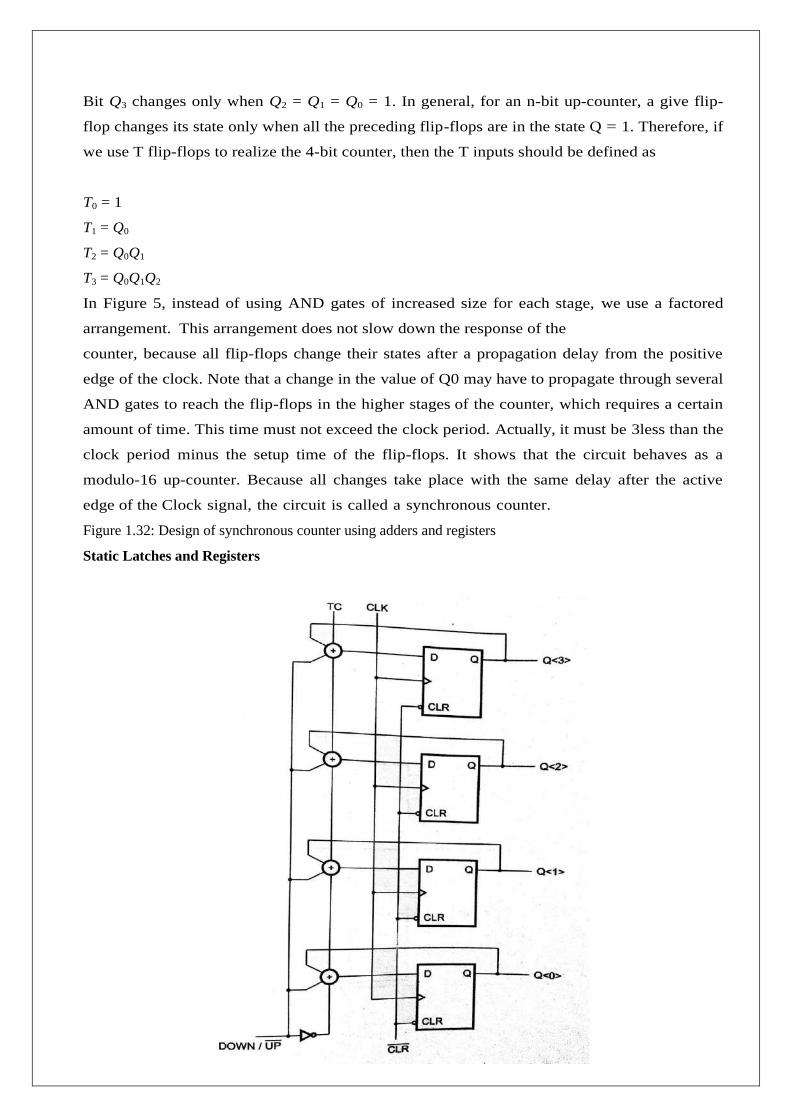
Bit Q3 changes only when Q2 = Q1 = Q0 = 1. In general, for an n-bit up-counter, a give flip-
flop changes its state only when all the preceding flip-flops are in the state Q = 1. Therefore, if
we use T flip-flops to realize the 4-bit counter, then the T inputs should be defined as
T0 = 1
T1 = Q0
T2 = Q0Q1
T3 = Q0Q1Q2
In Figure 5, instead of using AND gates of increased size for each stage, we use a factored
arrangement. This arrangement does not slow down the response of the
counter, because all flip-flops change their states after a propagation delay from the positive
edge of the clock. Note that a change in the value of Q0 may have to propagate through several
AND gates to reach the flip-flops in the higher stages of the counter, which requires a certain
amount of time. This time must not exceed the clock period. Actually, it must be 3less than the
clock period minus the setup time of the flip-flops. It shows that the circuit behaves as a
modulo-16 up-counter. Because all changes take place with the same delay after the active
edge of the Clock signal, the circuit is called a synchronous counter.
Figure 1.32: Design of synchronous counter using adders and registers
Static Latches and Registers

The Bistability Principle:
Static memories use positive feedback to create a bistable circuit — a circuit having two stable states that
represent 0 and 1. The basic idea is shown in Figure 7.4a, which shows two inverters connected in cascade
along with a voltage-transfer characteristic typical of such a circuit. Also plotted are the VTCs of the first
inverter, that is, Vo1 versus Vi1, and the second inverter (Vo2 versus Vo1). The latter plot is rotated to
accentuate that Vi2 =V o1. Assume now that the output of the second inverter Vo2 is connected to the input
of the first Vi1, as shown by the dotted lines in Figure 7.4a. The resulting circuit has only three possible
operation points (A, B, and C), as demonstrated on the combined VTC. The following important conjecture is
easily proven to be valid:
Under the condition that the gain of the inverter in the transient region is larger than 1, only Aand B are
stable operation points, and C is a metastable operation point.
SR Flip-Flops
The cross-coupled inverter pair shown in the previous section provides an approach to store a binary variable
in a stable way. However, extra circuitry must be added to enable control of the memory states. The
wellknow SR —or set-reset— flip-flop, an implementation of which is shown in Figure 7.6a. This circuit is
similar to the cross-coupled inverter pair with NOR gates replacing the inverters. The second input of the
NOR gates is connected to the trigger inputs (S and R),that make it possible to force the outputs Q and Q to a
given state. These outputs are complimentary (except for the SR = 11 state). When both S and R are 0, the
flip-flop is in a quiescent state and both outputs retain their value (a NOR gate with one of its input being 0
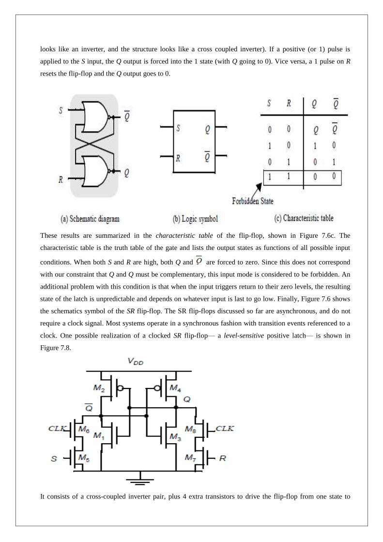
looks like an inverter, and the structure looks like a cross coupled inverter). If a positive (or 1) pulse is
applied to the S input, the Q output is forced into the 1 state (with Q going to 0). Vice versa, a 1 pulse on R
resets the flip-flop and the Q output goes to 0.
These results are summarized in the characteristic table of the flip-flop, shown in Figure 7.6c. The
characteristic table is the truth table of the gate and lists the output states as functions of all possible input
conditions. When both S and R are high, both Q and are forced to zero. Since this does not correspond
with our constraint that Q and Q must be complementary, this input mode is considered to be forbidden. An
additional problem with this condition is that when the input triggers return to their zero levels, the resulting
state of the latch is unpredictable and depends on whatever input is last to go low. Finally, Figure 7.6 shows
the schematics symbol of the SR flip-flop. The SR flip-flops discussed so far are asynchronous, and do not
require a clock signal. Most systems operate in a synchronous fashion with transition events referenced to a
clock. One possible realization of a clocked SR flip-flop— a level-sensitive positive latch— is shown in
Figure 7.8.
It consists of a cross-coupled inverter pair, plus 4 extra transistors to drive the flip-flop from one state to

another and to provide clocked operation. Observe that the number of transistors is identical to the
implementation of Figure 7.6, but the circuit has the added feature of being clocked. The drawback of saving
some transistors over a fully-complimentary CMOS implementation is that transistor sizing becomes critical
in ensuring proper functionality. Consider the case where Q is high and an R pulse is applied. The
combination of transistors M4, M7, and M8 forms a ratioed inverter. In order to make the latch switch, we
must succeed in bringing Q below the switching threshold of the inverter M1-M2. Once this is achieved, the
positive feedback causes the flip-flop to invert states. This requirement forces us to increase the sizes of
transistors M5, M6, M7, and M8.
Multiplexer-Based Latches
There are many approaches for constructing latches. One very common technique involves the use of
transmission gate multiplexers. Multiplexer based latches can provide similar functionality to the SR latch,
but has the important added advantage that the sizing of devices only affects performance and is not critical
to the functionality.
Figure 7.11 shows an implementation of static positive and negative latches based on multiplexers. For a
negative latch, when the clock signal is low, the input 0 of the multiplexer is selected, and the D input is
passed to the output. When the clock signal is high,the input 1 of the multiplexer, which connects to the
output of the latch, is selected. The feedback holds the output stable while the clock signal is high. Similarly
in the positive latch, the D input is selected when clock is high, and the output is held (using feedback) when
clock is low.
A transistor level implementation of a positive latch based on multiplexers is shown in Figure 7.12. When
CLK is high, the bottom transmission gate is on and the latch is
transparent - that is, the D input is copied to the Q output. During this phase, the feedback loop is open since
the top transmission gate is off. Unlike the SR FF, the feedback does not have to be overridden to write the
memory and hence sizing of transistors is not critical for realizing correct functionality. The number of
transistors that the clock touches is important since it has an activity factor of 1. This particular latch
implementation is not particularly efficient from this metric as it presents a load of 4 transistors to the CLK
signal.

It is possible to reduce the clock load to two transistors by using implement multiplexers using NMOS only
pass transistor as shown in Figure 7.13. The advantage of this approach is the reduced clock load of only two
NMOS devices. When CLK is high, the latch samples the D input, while a low clock-signal enables the
feedback-loop, and puts the latch in the hold mode. While attractive for its simplicity, the use of NMOS only
pass transistors results in the passing of a degraded high voltage of VDD-VTn to the input of the first
inverter. This impacts both noise margin and the switching performance, especially in the case of low values
of VDD and high values of VTn. It also causes static power dissipation in first inverter, as already pointed out
in Chapter 6. Since the maximum input-voltage to the inverter equals VDD-VTn, the PMOS device of the
inverter is never turned off,
resulting is a static current flow.
Master-Slave Edge-Triggered Register
The most common approach for constructing an edge-triggered register is to use a masterslave
configuration, as shown in Figure 7.14. The register consists of cascading a negative latch (master stage)
with a positive latch (slave stage). A multiplexer-based latch is used in this particular implementation,
although any latch could be used. On the low phase of the clock, the master stage is transparent, and the D
input is passed to the master stage output, using feedback.
On the rising edge of the clock, the master slave stops sampling the input, and the slave stage starts
sampling. During the high phase of the clock, the slave stage samples the output of the master stage (QM),
while the master stage remains in a hold mode. Since QM is constant during the high phase of the clock, the
output Q makes only one transition per cycle. The value of Q is the value of D right before the rising edge of
the clock, achieving the positive edge-triggered effect. A negative edge-triggered register can be constructed
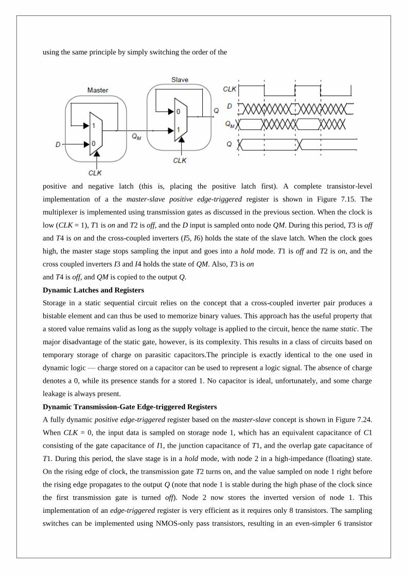
using the same principle by simply switching the order of the
positive and negative latch (this is, placing the positive latch first). A complete transistor-level
implementation of a the master-slave positive edge-triggered register is shown in Figure 7.15. The
multiplexer is implemented using transmission gates as discussed in the previous section. When the clock is
low (CLK = 1), T1 is on and T2 is off, and the D input is sampled onto node QM. During this period, T3 is off
and T4 is on and the cross-coupled inverters (I5, I6) holds the state of the slave latch. When the clock goes
high, the master stage stops sampling the input and goes into a hold mode. T1 is off and T2 is on, and the
cross coupled inverters I3 and I4 holds the state of QM. Also, T3 is on
and T4 is off, and QM is copied to the output Q.
Dynamic Latches and Registers
Storage in a static sequential circuit relies on the concept that a cross-coupled inverter pair produces a
bistable element and can thus be used to memorize binary values. This approach has the useful property that
a stored value remains valid as long as the supply voltage is applied to the circuit, hence the name static. The
major disadvantage of the static gate, however, is its complexity. This results in a class of circuits based on
temporary storage of charge on parasitic capacitors.The principle is exactly identical to the one used in
dynamic logic — charge stored on a capacitor can be used to represent a logic signal. The absence of charge
denotes a 0, while its presence stands for a stored 1. No capacitor is ideal, unfortunately, and some charge
leakage is always present.
Dynamic Transmission-Gate Edge-triggered Registers
A fully dynamic positive edge-triggered register based on the master-slave concept is shown in Figure 7.24.
When CLK = 0, the input data is sampled on storage node 1, which has an equivalent capacitance of C1
consisting of the gate capacitance of I1, the junction capacitance of T1, and the overlap gate capacitance of
T1. During this period, the slave stage is in a hold mode, with node 2 in a high-impedance (floating) state.
On the rising edge of clock, the transmission gate T2 turns on, and the value sampled on node 1 right before
the rising edge propagates to the output Q (note that node 1 is stable during the high phase of the clock since
the first transmission gate is turned off). Node 2 now stores the inverted version of node 1. This
implementation of an edge-triggered register is very efficient as it requires only 8 transistors. The sampling
switches can be implemented using NMOS-only pass transistors, resulting in an even-simpler 6 transistor

implementation. The reduced transistor count is attractive for high-performance and low-power systems. The
set-up time of this circuit is simply the delay of the transmission gate, and corresponds to the time it takes
node 1 to sample the D input. The hold time is approximately zero, since the transmission gate is turned off
on the clock edge and further inputs changes are ignored. The propagation delay (tc-q) is equal to two
inverter delays plus the delay of the transmission gate T2.One important consideration for such a dynamic
register is that the storage nodes (i.e., the state) has to be refreshed at periodic intervals to prevent a loss due
to charge leakage,due to diode leakage as well as sub-threshold currents. In datapath circuits, the refresh rate
is not an issue since the registers are periodically clocked, and the storage nodes are constantly
updated.Clock overlap is an important concern for this register. Consider the clock waveforms
shown in Figure 7.25. During the 0-0 overlap period, the NMOS of T1 and the PMOS of T2 are
simultaneously on, creating a direct path for data to flow from the D input of the register to the Q output.
This is known as a race condition. The output Q can changeon the falling edge if the overlap period is large
— obviously an undesirable effect for a positive edge-triggered register.
The same is true for the 1-1 overlap region, where an input-output path exists through the PMOS of T1 and
the NMOS of T2. The latter case is taken care off by enforcing a hold time constraint. That is, the data must
be stable during the high-high overlap period. The former situation (0-0 overlap) can be addressed by
making sure that there is enough delay between the D input and node 2 ensuring that new data sampled by
the master stage does not propagate through to the slave stage. Generally the
built in single inverter delay should be sufficient and the overlap period constraint is given
as: The set-up time of this circuit is simply the delay of the transmission gate, and corresponds
to the time it takes node 1 to sample the D input. The hold time is approximately
zero, since the transmission gate is turned off on the clock edge and further inputs changes
are ignored. The propagation delay (tc-q) is equal to two inverter delays plus the delay of
the transmission gate T2.
One important consideration for such a dynamic register is that the storage nodes
(i.e., the state) has to be refreshed at periodic intervals to prevent a loss due to charge leakage,
due to diode leakage as well as sub-threshold currents. In datapath circuits, the refresh
rate is not an issue since the registers are periodically clocked, and the storage nodes are
constantly updated.
Clock overlap is an important concern for this register. Consider the clock waveforms

shown in Figure 7.25. During the 0-0 overlap period, the NMOS of T1 and the
PMOS of T2 are simultaneously on, creating a direct path for data to flow from the D input
of the register to the Q output. This is known as a race condition. The output Q can change
on the falling edge if the overlap period is large — obviously an undesirable effect for a
positive edge-triggered register. The same is true for the 1-1 overlap region, where an
input-output path exists through the PMOS of T1 and the NMOS of T2. The latter case is
taken care off by enforcing a hold time constraint. That is, the data must be stable during
the high-high overlap period. The former situation (0-0 overlap) can be addressed by making
sure that there is enough delay between the D input and node 2 ensuring that new data
sampled by the master stage does not propagate through to the slave stage. Generally the
built in single inverter delay should be sufficient and the overlap period constraint is given
as:
toverlap 0-0 < tT1+tI1+tT2
The C2MOS Register
Figure 7.26 shows an ingenious positive edge-triggered register, based on a master-slave
concept insensitive to clock overlap. This circuit is called the C2MOS (Clocked CMOS)
register [Suzuki73], and operates in two phases.

1. CLK = 0 (CLK = 1): The first tri-state driver is turned on, and the master stage acts as an inverter sampling
the inverted version of D on the internal node X. The master stage is in the evaluation mode. Meanwhile, the
slave section is in a high-impedance mode, or in a hold mode. Both transistors M7 and M8 are off,
decoupling the output from the input. The output Q retains its previous value stored on the output capacitor
CL2.
2. The roles are reversed when CLK = 1: The master stage section is in hold mode (M3-M4 off), while the
second section evaluates (M7-M8 on). The value stored on CL1propagates to the output node through the
slave stage which acts as an inverter.

THANK YOU