Embed Size (px)
Citation preview

Lecture 8: Extrinsic semiconductors -mobility
Contents
1 Carrier mobility 11.1 Lattice scattering . . . . . . . . . . . . . . . . . . . . . . . . . 21.2 Impurity scattering . . . . . . . . . . . . . . . . . . . . . . . . 31.3 Conductivity in extrinsic semiconductors . . . . . . . . . . . . 4
2 Degenerate semiconductors 7
3 Amorphous semiconductors 8
1 Carrier mobility
Dopants in an intrinsic semiconductor perform two major functions
1. They increase carrier concentration of a particular polarity (i.e. elec-trons or holes) so that the overall conductivity is higher. Usually thisis orders of magnitude higher than the intrinsic semiconductor and isdominated by either electrons or holes i.e. the majority carriers.
2. Dopants also stabilize carrier concentration around room temperature.For Si, the saturation regime extends from roughly 60 K to 560 K.
Consider the general conductivity equation
σ = neµe + peµh (1)
For extrinsic semiconductors with either n or pmuch higher than the minoritycarrier concentration equation 1 can be written as
n type : σ = neµe
p type : σ = peµh
(2)
1
MM5017: Electronic materials, devices, and fabrication
µe and µh are the drift mobilities of the carriers. They are given by
µe =eτem∗
e
µh =eτhm∗
h
(3)
The drift mobilities are a function of temperature and in extrinsic semicon-ductors they depend on the dopant concentration. This dependence comesfrom the scattering time, τe and τh, which is the time between two scatteringevents.Another way of writing the scattering time is in terms of a scattering crosssection (S). This is given by
τ =1
S vth Ns
(4)
where vth is the mean speed of the electrons (thermal velocity) and Ns is thenumber of scatters per unit volume. The role of scatters and the effect onmobility can be considered by considering the two main types of scatters
1. Lattice atoms
2. Impurities - dopants
1.1 Lattice scattering
In an intrinsic semiconductor the carrier scattering is mainly due to thermalvibrations of the lattice (Si atoms). In metals, electron-electron scatteringis also important and affects the conductivity, but electron concentration insemiconductors are low so that electron-electron scattering can be ignored.For lattice scattering, if a is the amplitude of the lattice vibrations for asimple two dimensional scattering, S is just πa2. As temperature increases,a increases and hence S increases. The second term in equation 4 is thethermal velocity (vth). This is typically given by 3
2kBT . For an electron in
the conduction band this is equal to its kinetic energy so that
1
2m∗
evth =3
2kBT ⇒ vth ∝
√T (5)
The concentration of scatters, Ns, is a constant and is independent of tem-perature.
2
MM5017: Electronic materials, devices, and fabrication
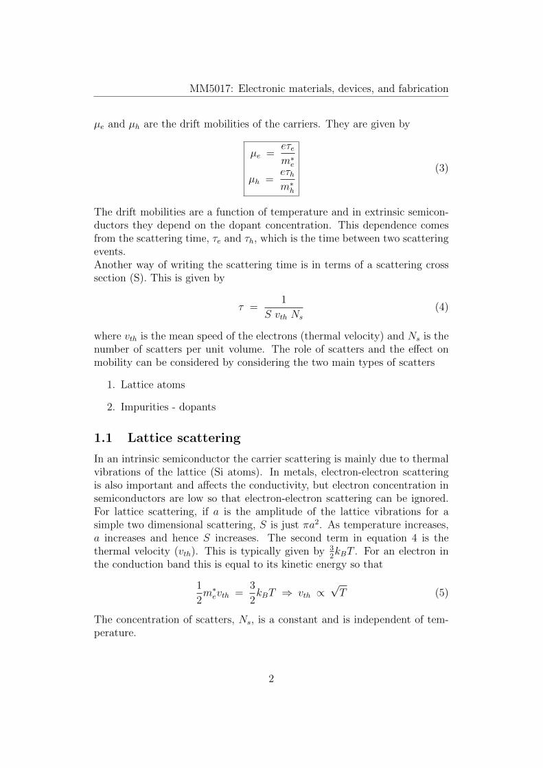
Figure 1: Electron scattering from an ionized As donor. The scattering crosssection is calculated considering the balance between the kinetic energy andthe potential energy, using which a scattering radius, rc, is defined. Adaptedfrom Principles of Electronic Materials - S.O. Kasap.
So the dependence of lattice scattering time (τL) on temperature can be givenusing equation 4
τL =1
(πa2)vthNs
∝ 1
(T )(T12 )
∝ T (− 32) (6)
Since the scattering time is directly proportional to the mobility, see equa-tion 3, this means that µe is also proportional to T (− 3
2). Thus, the effect
of lattice scattering is to reduce the mobility with increase in temperature.This can be understood qualitatively by seeing that as the temperature in-creases the atomic vibrations increase and at the same time the electrons alsotravel faster. Both these effects combine to reduce the mobility. A similarargument is valid for hole scattering in intrinsic semiconductors. Despite thisdecrease in mobility, conductivity increases with temperature because carrierconcentration increases exponentially with temperature.
1.2 Impurity scattering
Impurity scattering becomes important for doped semiconductors. At roomtemperature the impurities are ionized, so that there is an electrostatic at-traction between the electrons traveling in the lattice and the impurity, asshown in figure 1 for As doped in Si (donor). To find the scattering cross sec-tion due to the ionized impurities we can equate the kinetic energy (KE) ofthe electrons to the potential energy (PE) due to the ionized impurity. From
3

MM5017: Electronic materials, devices, and fabrication
figure 1 the electron will not be scattered if KE dominates while scatteringoccurs if PE dominates. The scattering radius, rc, is the distance at whichboth effects are equal
3
2kBT =
e2
4πε0εrrcS = πr2c ∝ T−2
(7)
So the scattering time due to impurities, τI , is given by equation 4
τI =1
(πr2c )vthNI
∝ 1
(T−2)(T12 )
∝ T32 (8)
Again, since the scattering time is directly related to mobility, the mobilitydue to impurities increases with temperature, opposite to the behavior ob-served with the lattice. This can be understood qualitatively by consideringthat with increasing temperature, electrons can travel faster and this makesit easier to escape the ionized impurities.
1.3 Conductivity in extrinsic semiconductors
In intrinsic semiconductors the only factor that affects mobility is the latticescattering so that mobility always reduces with temperature. In extrinsicsemiconductors there are two contributions - lattice (µL) and the impurities(µI). So the total mobility is given by Matthiessen’s rule, which is
1
µe
=1
µI
+1
µL
(9)
The scattering process with the lowest mobility dominates. Also, at low tem-peratures mobility actually increases with temperature since impurity scat-tering dominates, while at high temperature lattice scattering dominates.This is shown in figure 2. At low dopant concentrations lattice scatteringdominates over the entire temperature range. With increasing dopant con-centrations impurity scattering starts to dominate at low temperature. Asimilar behavior is also seen for hole mobility. Experimental measurementsof electron and hole mobilities in Si, as a function of temperature, are shownin figure 3 and confirm this behavior. Also, at constant temperature the mo-bility decreases with increasing dopant concentration since there is greaterconcentration of impurities, as shown in figure 4.Looking at the the temperature dependence of conductivity, both the carrier
concentration change and mobility change with temperature and influence
4

MM5017: Electronic materials, devices, and fabrication
Figure 2: Mobility vs. temperature for different donor concentrations forextrinsic semiconductors. For low Nd mobility decreases with temperature,but as Nd increases at low temperature mobility actually increases. Adaptedfrom Principles of Electronic Materials - S.O. Kasap.
Figure 3: Log-log plot of experimental (a) electron mobility and (b) holemobility vs. temperature for different dopant concentrations in Si. Theapplied electric field is small (low E). Source http://dx.doi.org/10.1016/0038-1101(77)90054-5
.
5

MM5017: Electronic materials, devices, and fabrication
Figure 4: Mobility vs. dopant concentrations for both donors and acceptors.In both cases the mobility decreases with increasing dopant concentration.Adapted from Principles of Electronic Materials - S.O. Kasap.
Figure 5: Conductivity dependence on T for extrinsic semiconductors. Thedependence closely follows the concentration of majority carriers vs. tem-perature, with the effect if mobility being felt in the saturation (extrinsic)regime. Adapted from Principles of Electronic Materials - S.O. Kasap.
6
MM5017: Electronic materials, devices, and fabrication
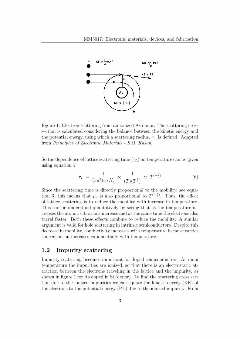
Figure 6: (a) Carrier concentration, (b) electron mobility and (c) conductiv-ity for Si doped with 1015 cm−3 donor atoms. The increase in carrier con-centration with temperature is balanced by the reduction in mobility. Thisis a semilog plot vs. inverse temperature (plotted in mK−1) and generatedusing MATLAB.
the conductivity. The temperature dependence of conductivity is shown infigure 5. The dominating term is still the carrier concentration, due to its ex-ponential dependence on T but the mobility term also plays a role, especiallyin the extrinsic regime (or saturation regime). Again, based on conductivitythere is an optimal temperature range where σ is nearly constant. For Si,this is around room temperature so that doping not only gives a temperatureindependent carrier concentration but also conductivity. For Si doped with1015 cm−3 donors the carrier concentration, mobility, and conductivity areplotted in figure 6.
2 Degenerate semiconductors
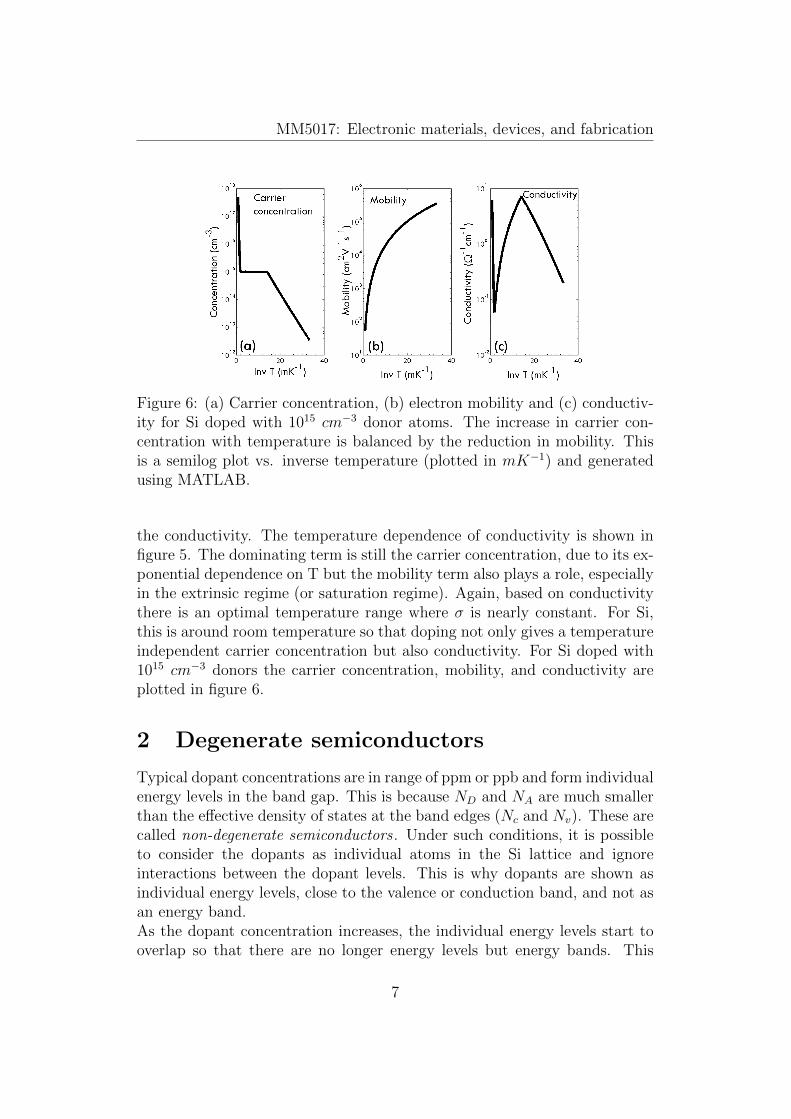
Typical dopant concentrations are in range of ppm or ppb and form individualenergy levels in the band gap. This is because ND and NA are much smallerthan the effective density of states at the band edges (Nc and Nv). These arecalled non-degenerate semiconductors . Under such conditions, it is possibleto consider the dopants as individual atoms in the Si lattice and ignoreinteractions between the dopant levels. This is why dopants are shown asindividual energy levels, close to the valence or conduction band, and not asan energy band.As the dopant concentration increases, the individual energy levels start tooverlap so that there are no longer energy levels but energy bands. This
7
MM5017: Electronic materials, devices, and fabrication
Figure 7: Degenerate (a) n and (b) p type semiconductors. The impuritiesform an energy band that can merge with either the valence or conductionband. The Fermi level lies within this band rather that in the band gap.Degenerate semiconductors hence have properties similar to metals. Adaptedfrom Principles of Electronic Materials - S.O. Kasap.
happens at typical dopant concentrations of 1019 and 1020 cm−3, comparableto Nc and Nv (1020 cm−3). These are called degenerate semiconductors,and their energy band diagram is shown schematically in figure 7. The dopantenergy levels can merge with the conduction or valence band, so that theFermi energy lies within the band. Thus, degenerate semiconductors behavemore like metals than semiconductors. Degenerate doped semiconductorsare used for some opto-electronic devices like lasers due to the large carrierconcentration.
3 Amorphous semiconductors
For most semiconductor applications, single crystal defect free materials areused. Typical metallic impurity concentration in Si used for integrated cir-cuit manufacture should be less than 0.1 ppb. Similarly, other defects, likedislocations, are harmful since they can modify the electronic properties ofthe material. The most common defect is the surface. Since the surface rep-resents a break in the material, there will be dangling bonds at the surface.These dangling bonds produce defects states that lie at the center of theband gap. These defects states can then ‘pin’ the Fermi level at the centerof the gap which will affect the carrier transport properties, especially whenjunctions or interfaces are formed with other materials. For Si, there is a na-
8

MM5017: Electronic materials, devices, and fabrication
Figure 8: Energy bands in a crystalline semiconductor. (a) Simple bandpicture showing the band edges. (b) Density of states in the valence andconduction band. There are no energy states in the forbidden energy gap.Adapted from Physics of Semiconductor Devices - S.M. Sze.
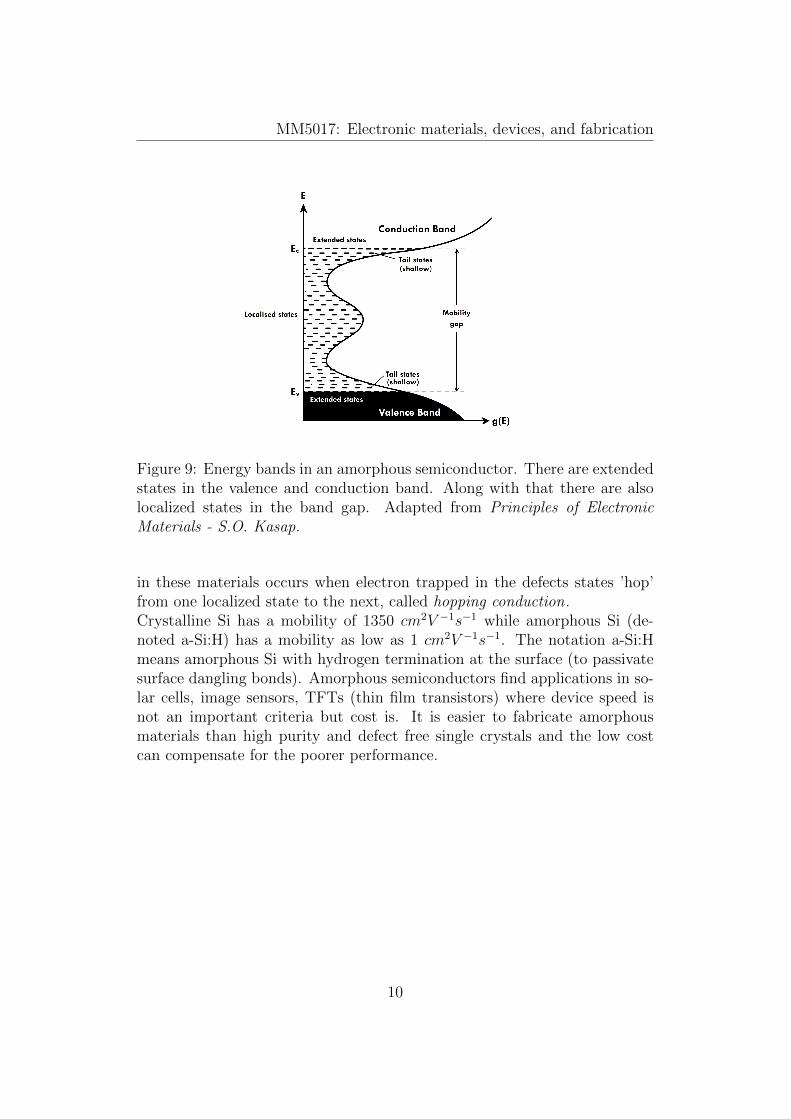
tive oxide layer (approximately 3 nm thick) that causes surface passivationand reduces the density of these dangling bonds.An amorphous semiconductor is an extreme example of the defective semi-conductor. Amorphous materials have no long range order and this leads toa large density of dangling bonds, not only at the surface but also the bulk.These dangling bonds lead to localized defect states in the band gap. Figure8 shows the energy bands in a crystalline semiconductor. There are no en-ergy states in the band gap i.e. the forbidden energy gap. The energy banddiagram for an amorphous semiconductor is shown in figure 9 and is dras-tically different from a crystalline semiconductor. There is the valence andconduction band, which form the extended states . They are the continuousenergy states, similar to a crystallline semiconductor. Along with them thedangling bonds produce localized states that lie within the band gap. Thesearise due to the lack of long range order in the amorphous material.The energy gap in an amorphous semiconductor is called a mobility gapbecause it is not a true band gap like crystalline semiconductors. In crystals,electrons cannot exist in the band gap because there are no available energystates. But in an amorphous semiconductor since there are localized statesin the band gap it is possible for electrons to exist in the band gap. Thelocalized states usually act as traps and reduce the mobility. Conductivity
9
MM5017: Electronic materials, devices, and fabrication
Figure 9: Energy bands in an amorphous semiconductor. There are extendedstates in the valence and conduction band. Along with that there are alsolocalized states in the band gap. Adapted from Principles of ElectronicMaterials - S.O. Kasap.
in these materials occurs when electron trapped in the defects states ’hop’from one localized state to the next, called hopping conduction.Crystalline Si has a mobility of 1350 cm2V −1s−1 while amorphous Si (de-noted a-Si:H) has a mobility as low as 1 cm2V −1s−1. The notation a-Si:Hmeans amorphous Si with hydrogen termination at the surface (to passivatesurface dangling bonds). Amorphous semiconductors find applications in so-lar cells, image sensors, TFTs (thin film transistors) where device speed isnot an important criteria but cost is. It is easier to fabricate amorphousmaterials than high purity and defect free single crystals and the low costcan compensate for the poorer performance.
10


![Lec8[1]Multiplicadores de Lagrange](https://img.dokumen.tips/doc/110x75/577cd5521a28ab9e789a79ff/lec81multiplicadores-de-lagrange.jpg)