Embed Size (px)
Citation preview

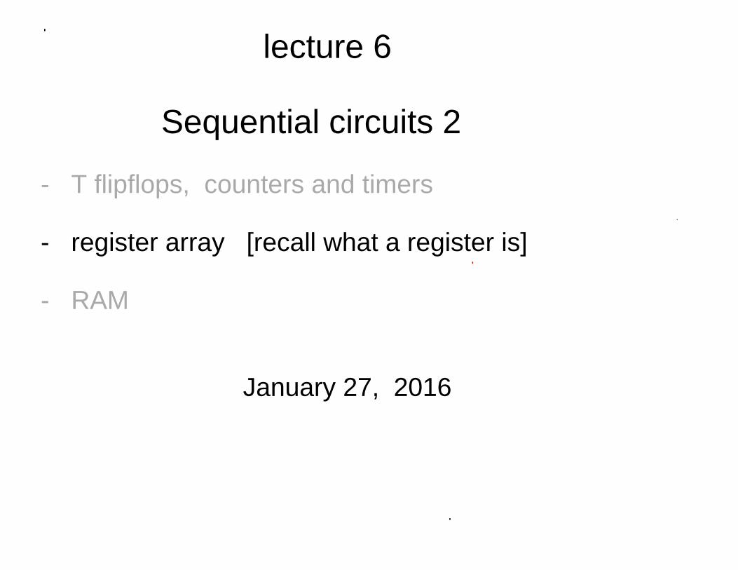
lecture 6
Sequential circuits 2
- T flipflops, counters and timers (finishing last lecture)
- register array
- RAM
January 27, 2016

TODAY: from flip flops to RAM
cm
m

T flip flop (toggle)
Assume falling edgetriggered.

Q: What does this circuit do ?
Assume falling edge triggered flip flops.
Qi is the clock input for flip flop i + 1.
i increases from left to right.


Correction of incorrect claim made from last lecture (see below).
D flip flop ("rising edge triggered")
By putting the inverter on the first D latch, we would make Qchange its value on the rising edge of the clock. There is noadvantage to this, so for simplicity we will always work with fallingedge triggered.
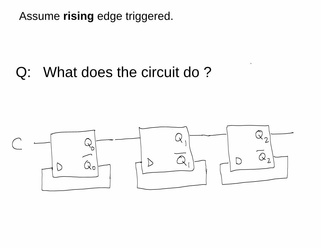
Assume rising edge triggered.
Q: What does the circuit do ?
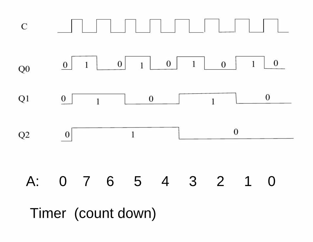
A: 0 7 6 5 4 3 2 1 0
Timer (count down)
lecture 6
Sequential circuits 2
- T flipflops, counters and timers
- register array [recall what a register is]
- RAM
January 27, 2016
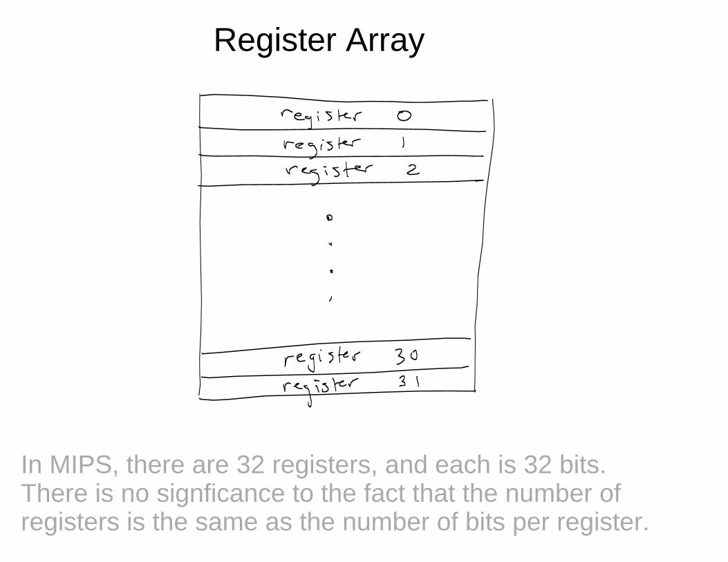
Register Array
In MIPS, there are 32 registers, and each is 32 bits.There is no signficance to the fact that the number ofregisters is the same as the number of bits per register.
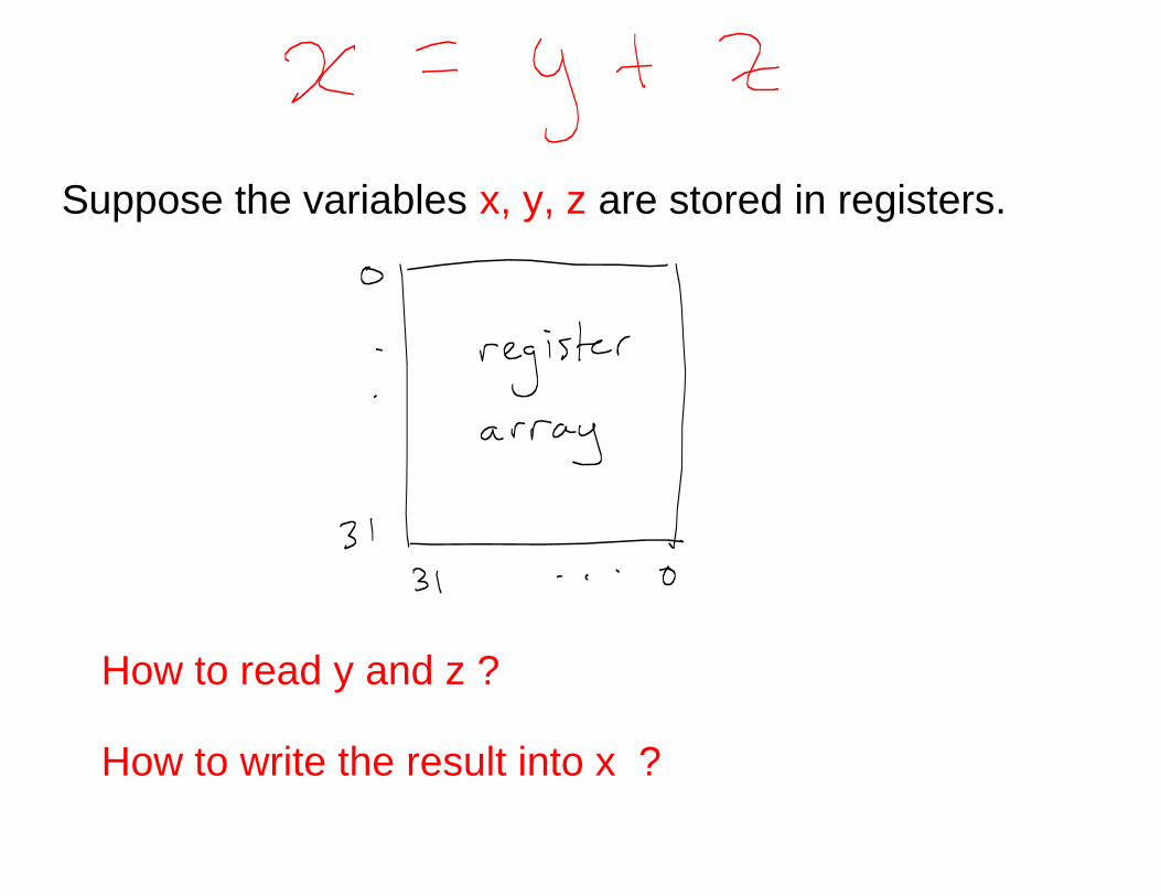
Suppose the variables x, y, z are stored in registers.
How to read y and z ?
How to write the result into x ?

Recall idea from lastlecture:
Use sets of D flip flops(register) to store numbersA and B.
Compute A + B using thecircuit shown, and write thenew value back into B.
For the next slide, we will willrotate A and B so they arehorizontall oriented and have32 of them (not 2), each 32bits (not 8).
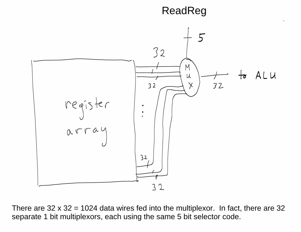
ReadReg
There are 32 x 32 = 1024 data wires fed into the multiplexor. In fact, there are 32separate 1 bit multiplexors, each using the same 5 bit selector code.

ReadReg1
ReadReg2
specify whichregister is y
specify whichregister is z

WriteEnable
WriteReg 5-to-32decoder
WriteData
specify whichregister is x

[ADDED SLIDE]
I neglected to mention in the lecture that the clock signalC is embedded in the WriteEnable signal. That is,WriteEnable = 1 if the clock C is 1. Note this is not an"if or only if", rather
WriteEnable = AND( C, ....)
I won't write the clock explicitly in the future since it isunderstood that when we are working with registers, wealways need a clock to synchronize the writes.
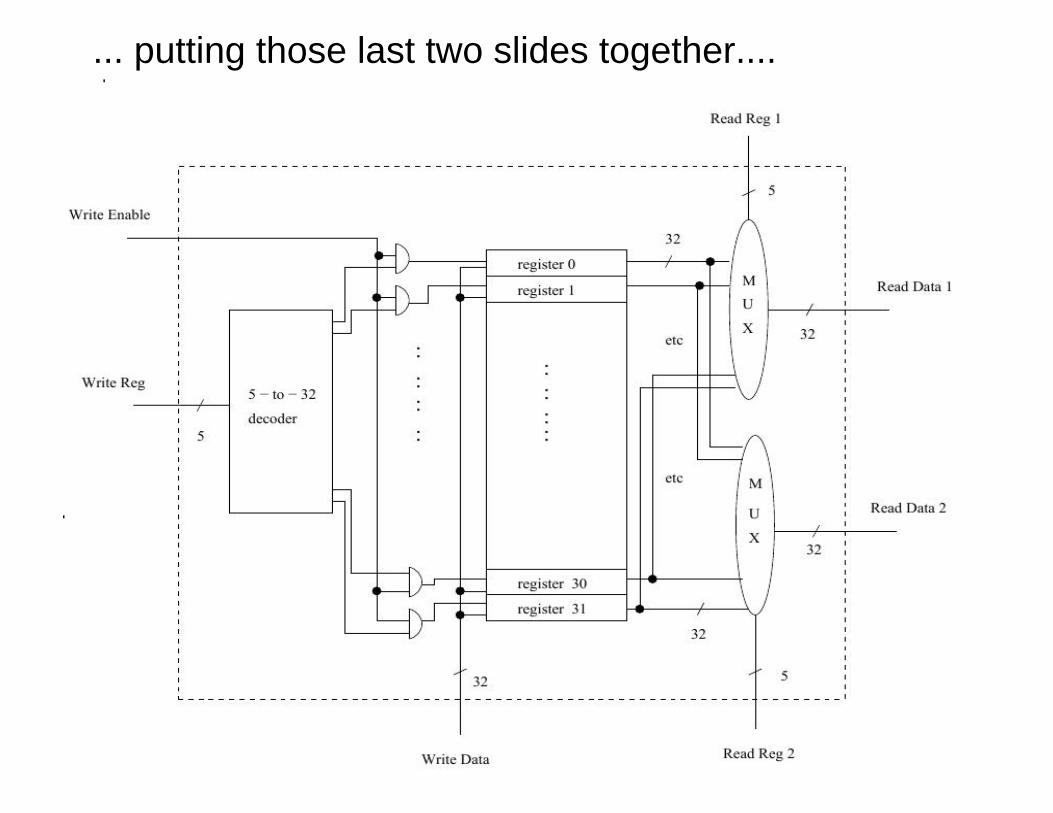
... putting those last two slides together....
WriteEnable
ReadReg1
ReadReg2
WriteReg
WriteData
ReadData1
ReadData2
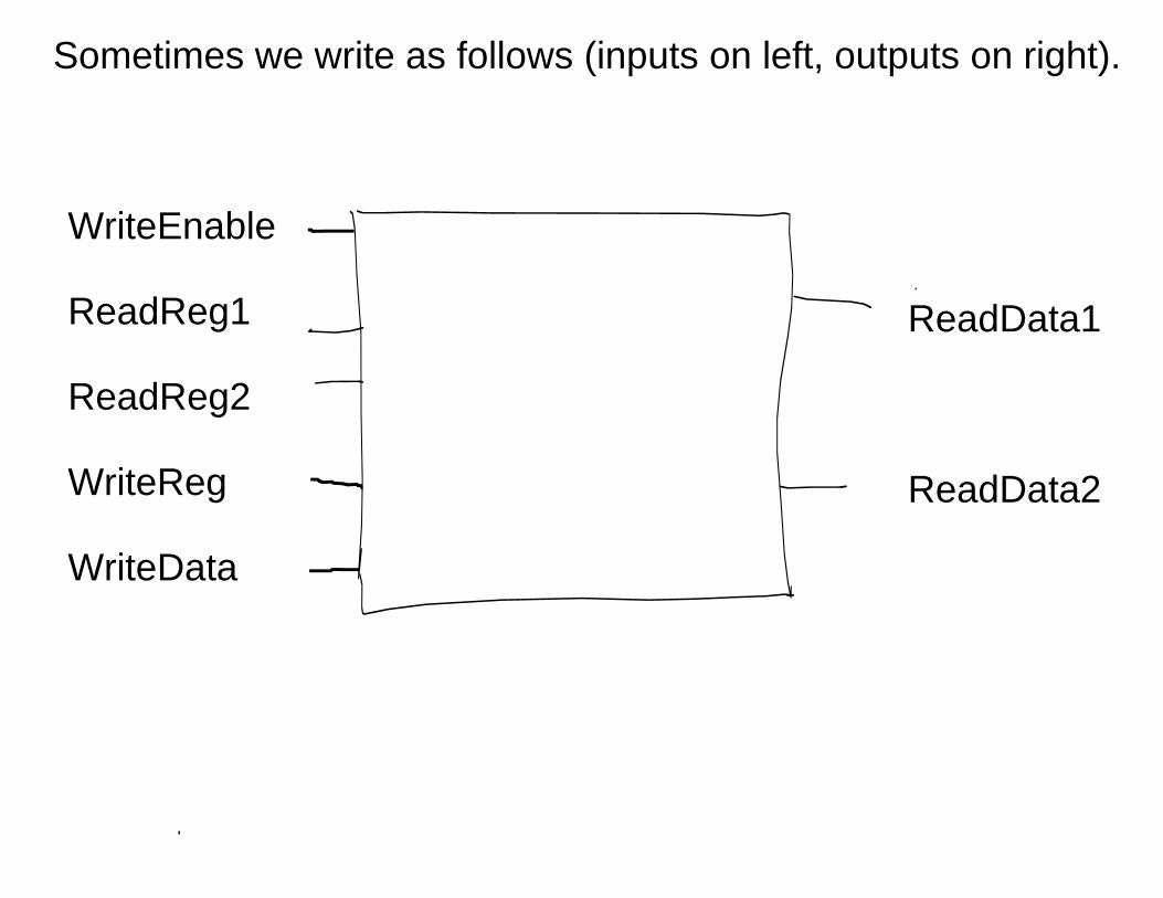
Sometimes we write as follows (inputs on left, outputs on right).

WriteEnable
ReadReg1ReadReg2WriteReg
WriteData
ReadData1
ReadData2
addressdata types of signalscontrol
operation

For larger memory arrays, the multiplexor design is notphysically feasible. You need N^2 wires coming out.But the side of the square array only grows with N.

An alternative approach ? .... somehow have only 2N wires,namely a read and a write wire for each column.
WriteData ReadData
MemWrite
clock C
RowSelect(alreadydecoded)
WriteEnable
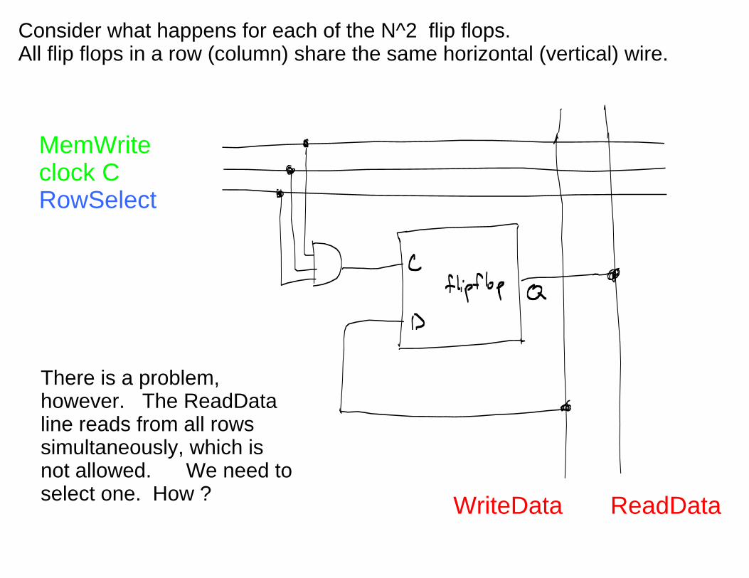
There is a problem,however. The ReadDataline reads from all rowssimultaneously, which isnot allowed. We need toselect one. How ? WriteData ReadData
MemWriteclock CRowSelect
Consider what happens for each of the N^2 flip flops.All flip flops in a row (column) share the same horizontal (vertical) wire.
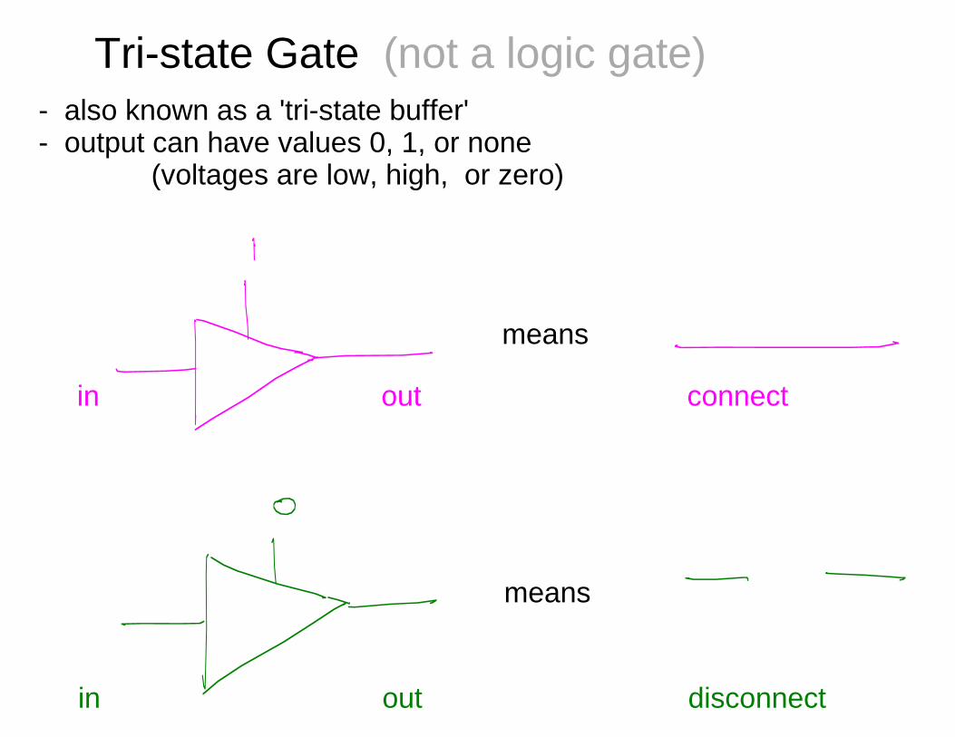
Tri-state Gate (not a logic gate)- also known as a 'tri-state buffer'- output can have values 0, 1, or none (voltages are low, high, or zero)
means
means
in out connect
in out disconnect

RowSelectMemWriteclock C
WriteData ReadData
The idea is thatonly one row isconnected to theReadData line.
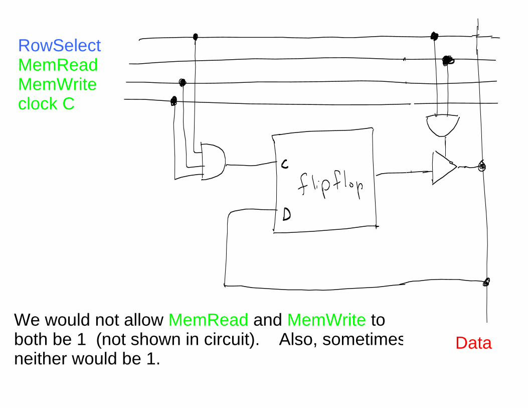
We would not allow MemRead and MemWrite toboth be 1 (not shown in circuit). Also, sometimesneither would be 1.
RowSelectMemReadMemWriteclock C
Data
MemWrite
MemRead
clock C
RowSelect(already decoded)
Data
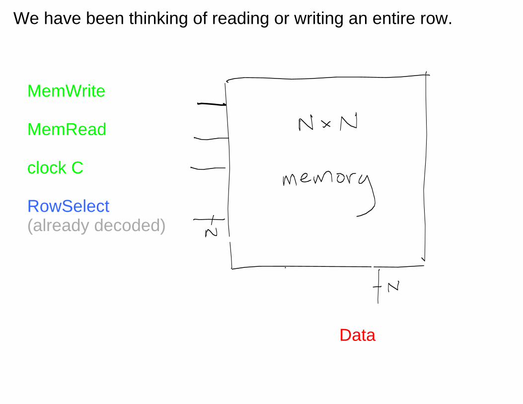
We have been thinking of reading or writing an entire row.
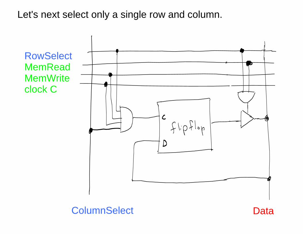
RowSelectMemReadMemWriteclock C
DataColumnSelect
Let's next select only a single row and column.
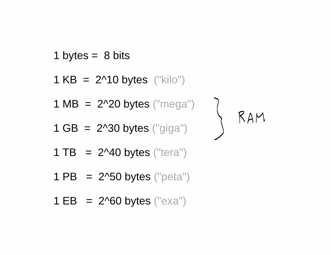
1 bytes = 8 bits
1 KB = 2^10 bytes ("kilo")
1 MB = 2^20 bytes ("mega")
1 GB = 2^30 bytes ("giga")
1 TB = 2^40 bytes ("tera")
1 PB = 2^50 bytes ("peta")
1 EB = 2^60 bytes ("exa")

e.g. Consider 8 chips with 2^16 x 2^15bits on each chip.
This defines 2^31 bits per chipor 2^31 bytes (2 GB).

MemReadMemWriteclock C
RowSelect
ColumnSelect
Data
rowdecoder
columndecoder

Announcements
- Quiz 1 and yellow stickies
- Quizzes: who writes in Arts 145 ? (70 seats) Quiz 2 A-H (lastname starts with...) Quiz 3 I - P Quiz 4 I - P Quiz 5 R-Z Quiz 6 R-Z
- Assignment 1 posted ~next Monday, download 'logisim' (there will be a demo on class on Monday)