Embed Size (px)
Citation preview

Lecture 5 - 1Introduction to Digital Integrated Circuit DesignTiming and Interconnect Issues
Lecture 5
Timing and Interconnect Issues
Konstantinos MasselosDepartment of Electrical & Electronic Engineering
Imperial College London
URL: http://cas.ee.ic.ac.uk/~kostasE-mail: [email protected]

Lecture 5 - 2Introduction to Digital Integrated Circuit DesignTiming and Interconnect Issues
Based on slides/material by…
J. Rabaey http://bwrc.eecs.berkeley.edu/Classes/IcBook/instructors.html“Digital Integrated Circuits: A Design Perspective”, Prentice Hall
D. Harris http://www.cmosvlsi.com/coursematerials.htmlWeste and Harris, “CMOS VLSI Design: A Circuits and Systems Perspective”, Addison Wesley
Lecture 5 - 3Introduction to Digital Integrated Circuit DesignTiming and Interconnect Issues
Recommended Reading
J. Rabaey et. al. “Digital Integrated Circuits: A Design Perspective”: Chapters 4, 9
Weste and Harris, “CMOS VLSI Design: A Circuits and Systems Perspective”: Chapter 4 (4.5, 4.6), Chapter 12 (12.5)
Lecture 5 - 4Introduction to Digital Integrated Circuit DesignTiming and Interconnect Issues
Outline
Timing• Clocking• Self timed and asynchronous design• Synchronization
Interconnect• Wire geometry• Capacitance effects• Wire engineering

Lecture 5 - 5Introduction to Digital Integrated Circuit DesignTiming and Interconnect Issues
Clock - key to synchronous systems
Synchronous systems use a clock to keep operations in sequence• Distinguish this from previous or next• Determine speed at which machine operates
Clock must be distributed to all the sequencing elements• Flip-flops and latches
Also distribute clock to other elements • Domino circuits and memories
Clocks help the design of FSM where outputs depend on both input and previous states

Lecture 5 - 6Introduction to Digital Integrated Circuit DesignTiming and Interconnect Issues
Clock Distribution
On a small chip, the clock distribution network is just a wire• And possibly an inverter for clkb
On practical chips, the RC delay of the wire resistance and gate load is very long• Variations in this delay cause clock to get to different elements at different
times• This is called clock skew
Most chips use repeaters to buffer the clock and equalize the delay• Reduces but doesn’t eliminate skew

Lecture 5 - 7Introduction to Digital Integrated Circuit DesignTiming and Interconnect Issues
The Clock Skew Problem
CL1 R1 CL2 R2 CL3 R3In Out
φ
tφ’ tφ’’ tφ’’’
tl,mintl,max
tr,mintr,max
ti
Clock Edge Timing Depends upon Position
Clock Rates as High as 500 Mhz in CMOS!

Lecture 5 - 8Introduction to Digital Integrated Circuit DesignTiming and Interconnect Issues
Clock Skew Sources
Systematic
Random
Drift
Jitter
Lecture 5 - 9Introduction to Digital Integrated Circuit DesignTiming and Interconnect Issues
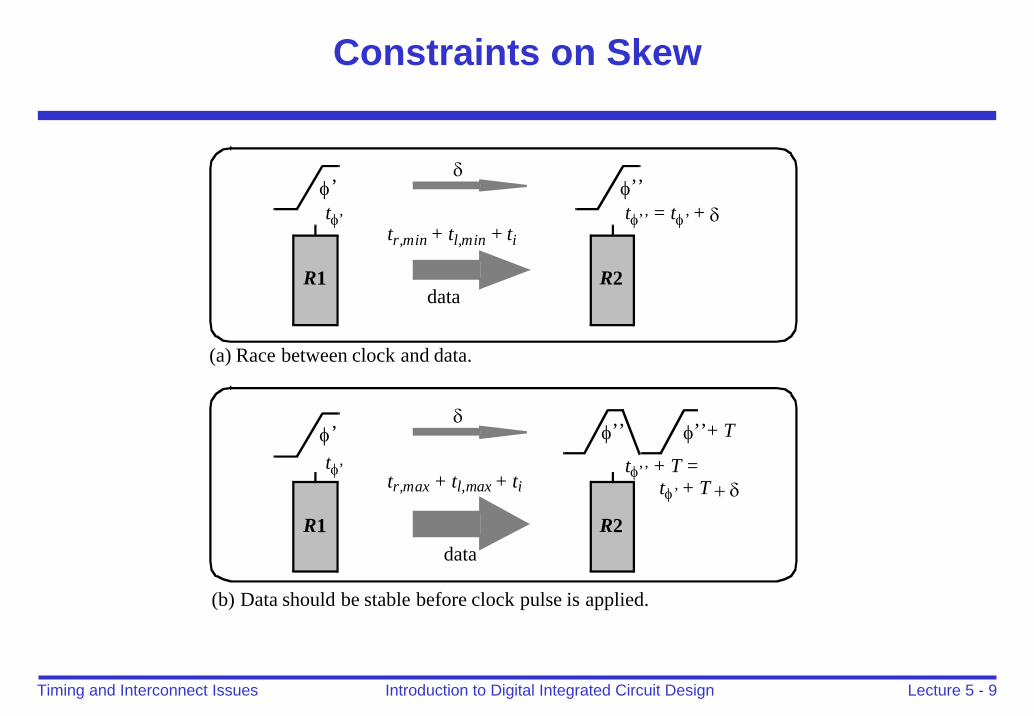
Constraints on Skew
R1 R2
φ’ φ’’δ
tr,min + tl,min + ti
(a) Race between clock and data.
R1 R2
φ’ φ’’+ Tδ
tr,max + tl,max + ti
(b) Data should be stable before clock pulse is applied.
tφ’ tφ’’ = tφ’ + δ
tφ’ tφ’’ + T =
data
data
φ’’
tφ’ + T + δ
Lecture 5 - 10Introduction to Digital Integrated Circuit DesignTiming and Interconnect Issues
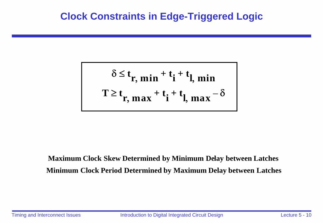
Clock Constraints in Edge-Triggered Logic
δ tr min, ti tl min,+ +≤
T tr max, ti tl max, δ–+ +≥
Maximum Clock Skew Determined by Minimum Delay between LatchesMinimum Clock Period Determined by Maximum Delay between Latches
Lecture 5 - 11Introduction to Digital Integrated Circuit DesignTiming and Interconnect Issues
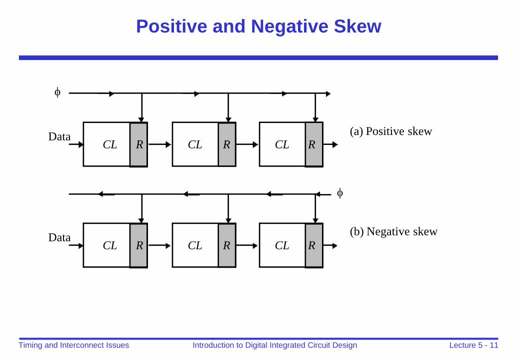
Positive and Negative Skew
R CL R CL RData
φ
CL
R CL R CL RData
CL
φ
(a) Positive skew
(b) Negative skew

Lecture 5 - 12Introduction to Digital Integrated Circuit DesignTiming and Interconnect Issues
Clock Skew in Master-Slave Two Phase Design
M1CL1 CL2 CL3In
φ2
S1 S2 S3M2
M3
φ1
φ1
φ2’φ1’
Lecture 5 - 13Introduction to Digital Integrated Circuit DesignTiming and Interconnect Issues
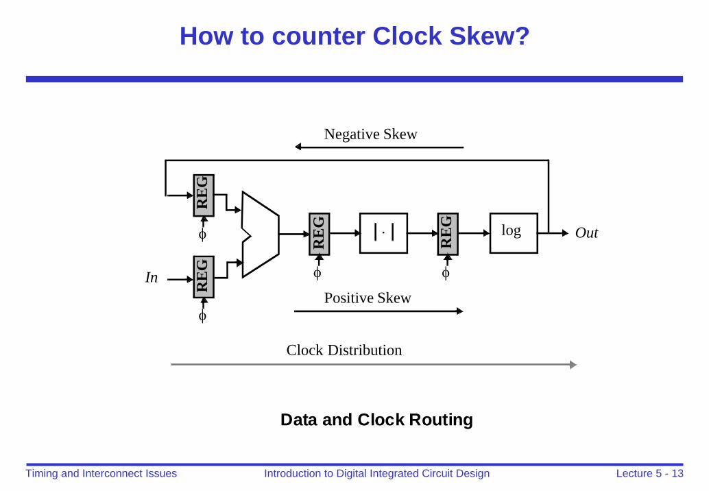
How to counter Clock Skew?
RE
G
φ
RE
G
φR
EG
φ
.
RE
G
φ
log Out
In
Clock Distribution
Positive Skew
Negative Skew
Data and Clock Routing
Lecture 5 - 14Introduction to Digital Integrated Circuit DesignTiming and Interconnect Issues
Solutions
Reduce clock skew• Careful clock distribution network design• Plenty of metal wiring resources
Analyze clock skew• Only budget actual, not worst case skews• Local vs. global skew budgets
Tolerate clock skew• Choose circuit structures insensitive to skew
Lecture 5 - 15Introduction to Digital Integrated Circuit DesignTiming and Interconnect Issues
Clock Distribution Networks
Ad hocGridsH-treeSpinesHybrid

Lecture 5 - 16Introduction to Digital Integrated Circuit DesignTiming and Interconnect Issues
Clock Grids
Use grid on two or more levels to carry clockMake wires wide to reduce RC delayEnsures low skew between nearby pointsBut possibly large skew across die
Lecture 5 - 17Introduction to Digital Integrated Circuit DesignTiming and Interconnect Issues
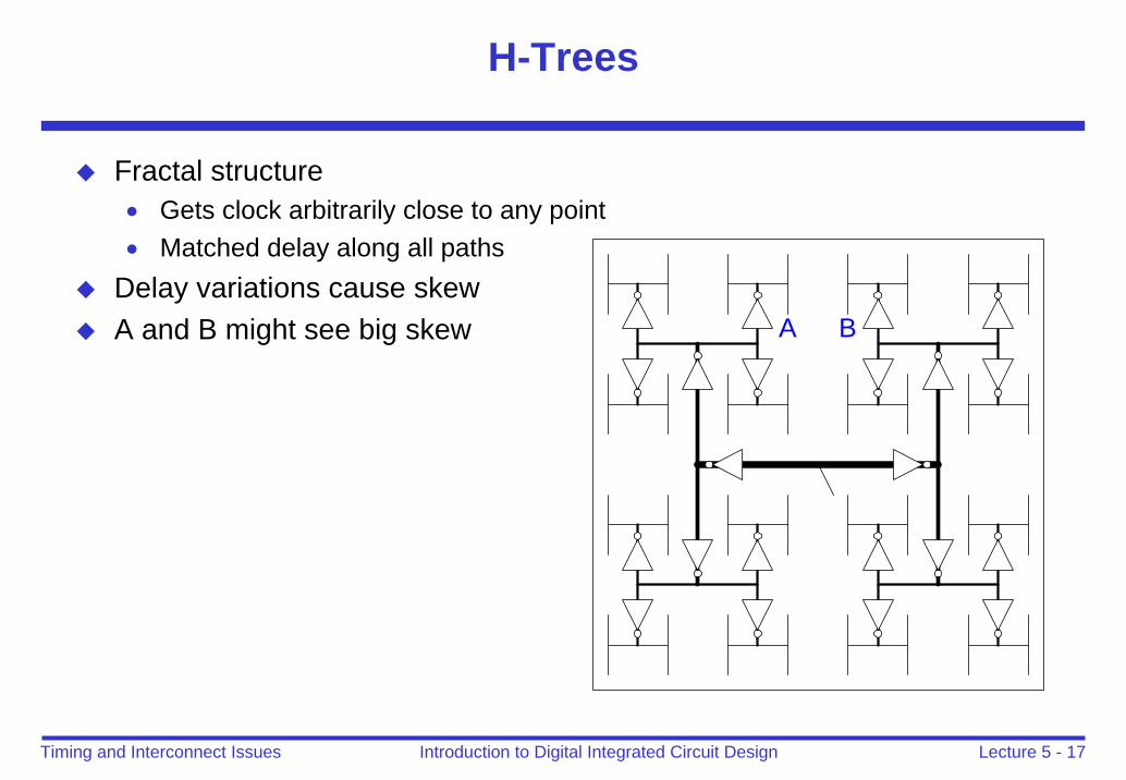
H-Trees
Fractal structure• Gets clock arbitrarily close to any point• Matched delay along all paths
Delay variations cause skewA and B might see big skew A B
Lecture 5 - 18Introduction to Digital Integrated Circuit DesignTiming and Interconnect Issues
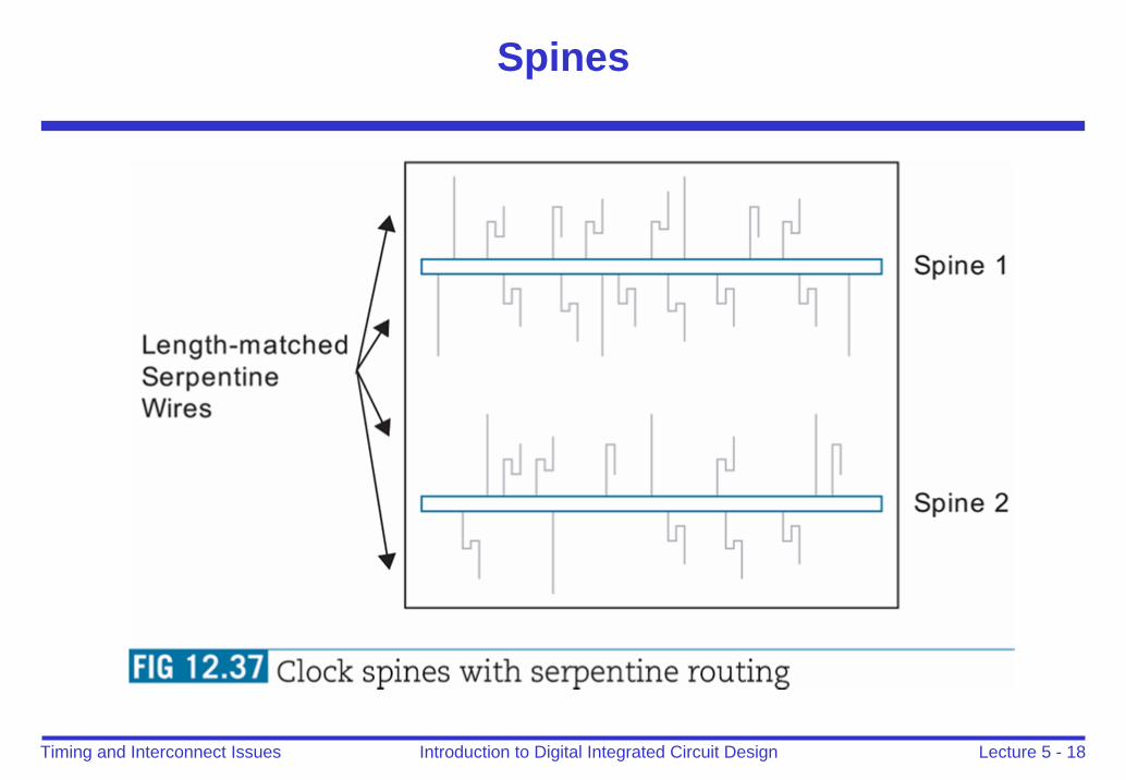
Spines

Lecture 5 - 19Introduction to Digital Integrated Circuit DesignTiming and Interconnect Issues
Hybrid Networks
Use H-tree to distribute clock to many pointsTie these points together with a grid
Ex: IBM Power4, PowerPC• H-tree drives 16-64 sector buffers• Buffers drive total of 1024 points• All points shorted together with grid

Lecture 5 - 20Introduction to Digital Integrated Circuit DesignTiming and Interconnect Issues
Outline
Timing• Clocking• Self timed and asynchronous design• Synchronization
Interconnect• Wire geometry• Capacitance effects• Wire engineering

Lecture 5 - 21Introduction to Digital Integrated Circuit DesignTiming and Interconnect Issues
Self-timed and asynchronous design
Functions of clock in synchronous design
1) Acts as completion signal2) Ensures the correct ordering of events
Truly asynchronous design
2) Ordering of events is implicit in logic1) Completion is ensured by careful timing analysis
Self-timed design
1) Completion ensured completion signal2) Ordering imposed by handshaking protocol
Lecture 5 - 22Introduction to Digital Integrated Circuit DesignTiming and Interconnect Issues
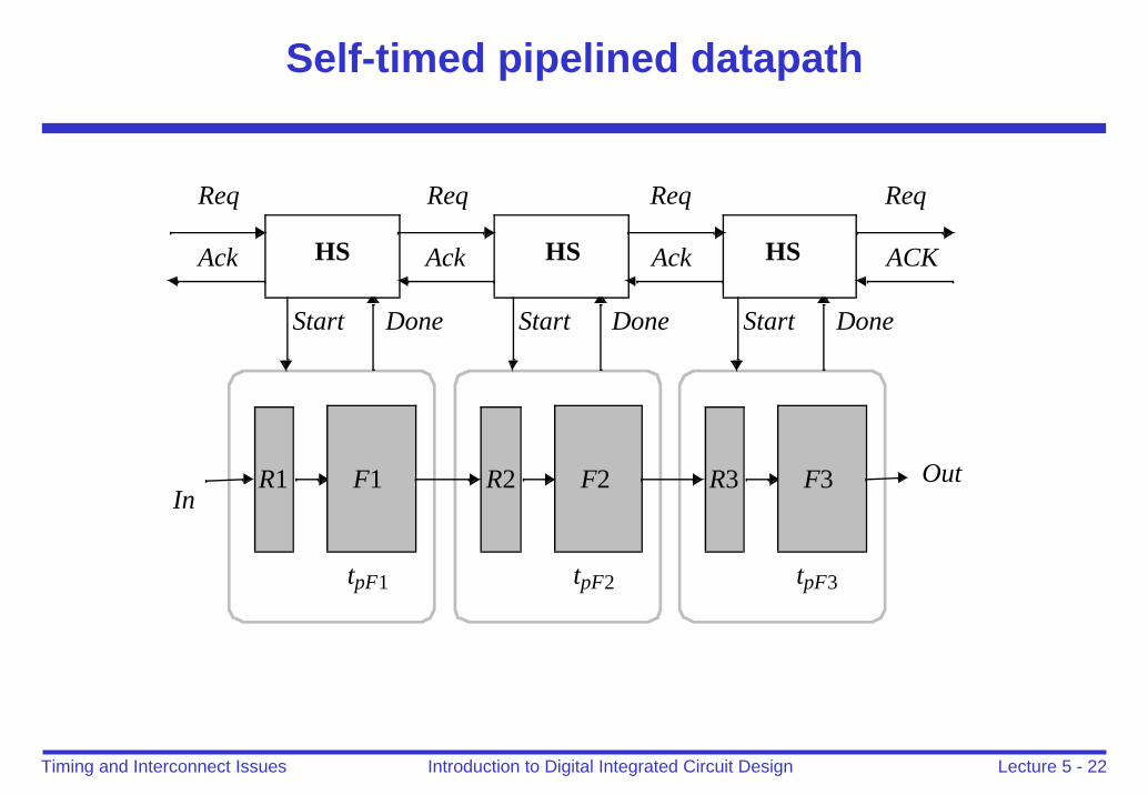
Self-timed pipelined datapath
R2 OutF2In
tpF2
Start Done
R1 F1
tpF1
Start Done
R3 F3
tpF3
Start Done
Req Req Req Req
Ack Ack Ack ACKHS HS HS

Lecture 5 - 23Introduction to Digital Integrated Circuit DesignTiming and Interconnect Issues
Completion Signal Generation
LOGIC
NETWORK
DELAY MODULE
In Out
Start Done
Using Delay Element (e.g. in memories)

Lecture 5 - 24Introduction to Digital Integrated Circuit DesignTiming and Interconnect Issues
Completion Signal Generation
Using Redundant Signal Encoding

Lecture 5 - 25Introduction to Digital Integrated Circuit DesignTiming and Interconnect Issues
Completion Signal in DCVSL
PDN
B0
PDNIn1In1In2In2
B1
Start
Start
VDD VDD
DoneB0
B1
Lecture 5 - 26Introduction to Digital Integrated Circuit DesignTiming and Interconnect Issues
Self-timed Adder
P0
C0
P1
G0
P2
G1
P3
G2 G3
VDD
Start
Start
P0
C0
P1
K0
P2
K1
P3
K2 K3
VDD
Start
Start
C0 C1 C2 C3 C4 C4
C4C0 C1 C2 C3 C4
VDD
Start
C4
C3
C2
C1
C4
C3
C2
C1
Start Done
(a) Differential carry generation
(b) Completion signal
Lecture 5 - 27Introduction to Digital Integrated Circuit DesignTiming and Interconnect Issues
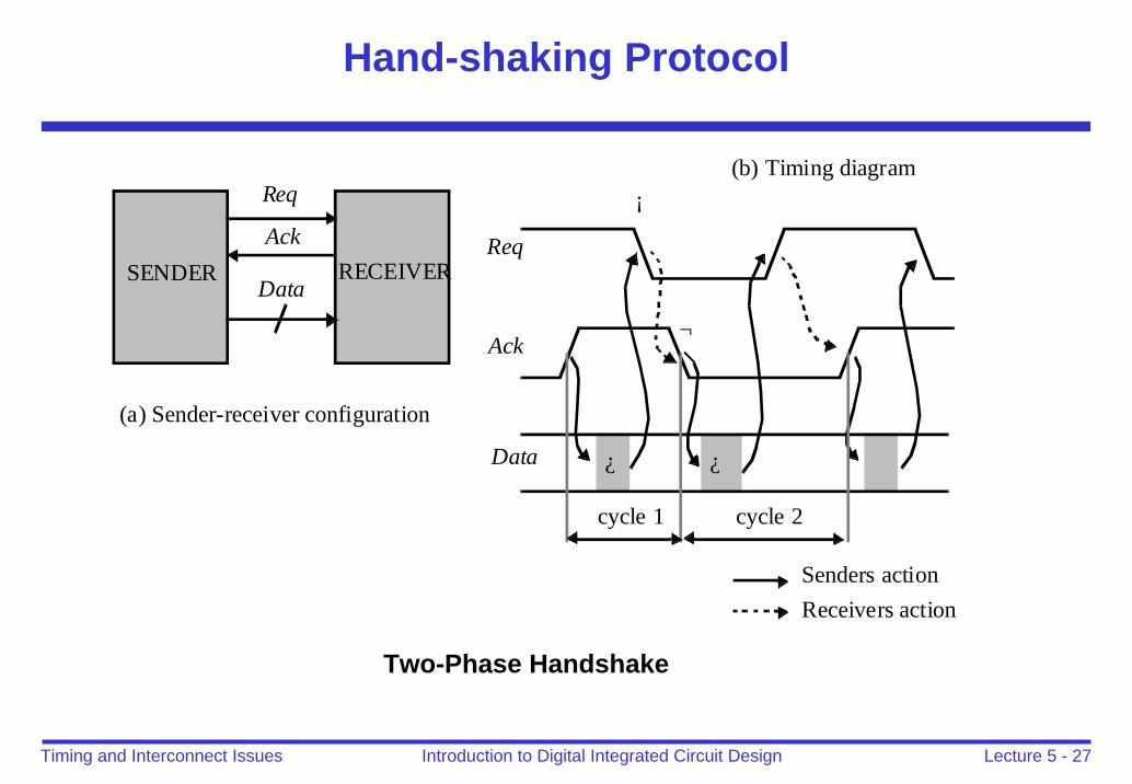
Hand-shaking Protocol
Req
Ack
DataSENDER RECEIVER
Senders actionReceivers action
Req
Ack
Data
cycle 1 cycle 2
¿ ¿
¡
¬
(a) Sender-receiver configuration
(b) Timing diagram
Two-Phase Handshake

Lecture 5 - 28Introduction to Digital Integrated Circuit DesignTiming and Interconnect Issues
Event Logic — The Muller C-element
C
A
B
F
A B Fn+1
0011
0101
0FnFn1
(a) Schematic (b) Truth table
VDD
FA
B
QS
R
A
BF
Static
Dynamic

Lecture 5 - 29Introduction to Digital Integrated Circuit DesignTiming and Interconnect Issues
2-phase Handshake Protocol
C
Sender
logic
Receiver
logic
Data
Data Ready
Req
Ack
Data Accepted
Handshake logic

Lecture 5 - 30Introduction to Digital Integrated Circuit DesignTiming and Interconnect Issues
4-phase Handshake Protocol (or RTZ)
Sender’s ActionReceiver’s ActionReq
Ack
Data
cycle 1 cycle 2
¿ ¿
¡
¬
Ð
ƒ

Lecture 5 - 31Introduction to Digital Integrated Circuit DesignTiming and Interconnect Issues
4-phase Handshake Protocol - Implementation
C
Sender
logic
Receiver
logic
Data
Data Ready
Req
Ack
Data Accepted
C
Handshake logic
S
Lecture 5 - 32Introduction to Digital Integrated Circuit DesignTiming and Interconnect Issues
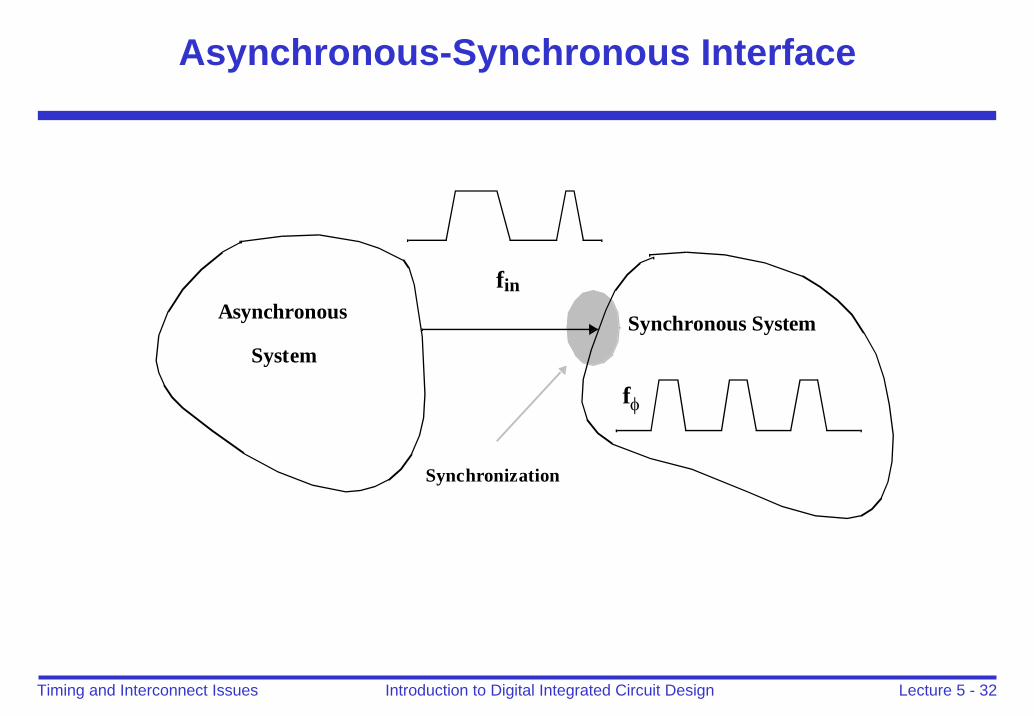
Asynchronous-Synchronous Interface
Asynchronous
SystemSynchronous System
fφ
fin
Synchronization

Lecture 5 - 33Introduction to Digital Integrated Circuit DesignTiming and Interconnect Issues
Outline
Timing• Clocking• Self timed and asynchronous design• Synchronization
Interconnect• Wire geometry• Capacitance effects• Wire engineering
Lecture 5 - 34Introduction to Digital Integrated Circuit DesignTiming and Interconnect Issues
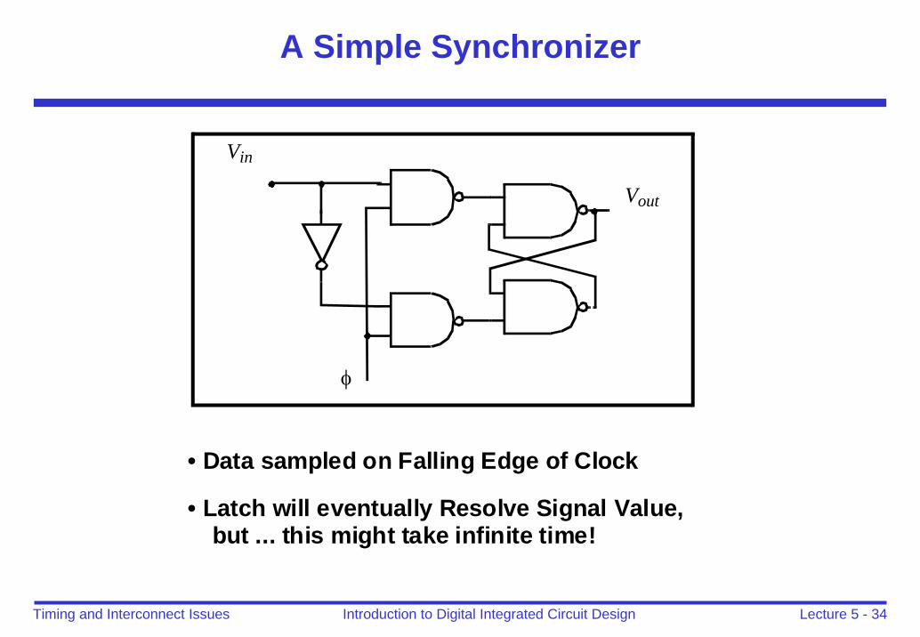
A Simple Synchronizer
φ
Vin
Vout
• Data sampled on Falling Edge of Clock
• Latch will eventually Resolve Signal Value,but ... this might take infinite time!

Lecture 5 - 35Introduction to Digital Integrated Circuit DesignTiming and Interconnect Issues
Arbiters
Req1
Req2
Req1
Req2
Ack1
Ack2Arbiter
Ack1
Ack2
(a) Schematic symbol
(b) Implementation
A
B
Req1
Req2
A
BAck1 t
(c) Timing diagramVT gap
metastable
Lecture 5 - 36Introduction to Digital Integrated Circuit DesignTiming and Interconnect Issues
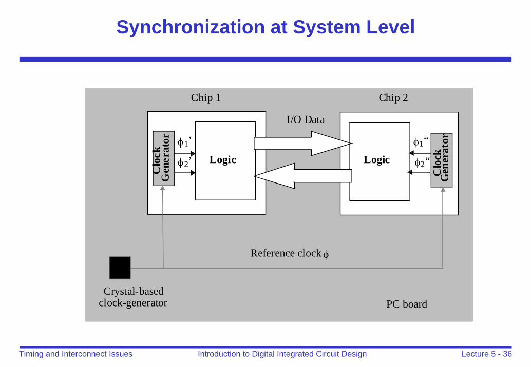
Synchronization at System Level
Reference clock φ
PC board
Chip 1 Chip 2
Logic Logic
I/O Data
φ1’
φ2’
φ1“
φ2“
Crystal-basedclock-generator
Clo
ckG
ener
ator
Clo
ckG
ener
ator
Lecture 5 - 37Introduction to Digital Integrated Circuit DesignTiming and Interconnect Issues
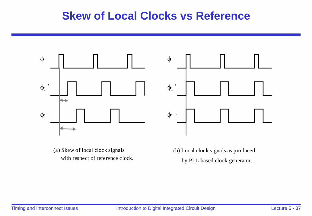
Skew of Local Clocks vs Reference
φ
φ1’
φ1"
φ
φ1’
φ1"
(a) Skew of local clock signalswith respect of reference clock.
(b) Local clock signals as produced
by PLL based clock generator.

Lecture 5 - 38Introduction to Digital Integrated Circuit DesignTiming and Interconnect Issues
Phase-Locked Loop Based Clock Generator
Phasedetector
Chargepump
Up
Down
Loopfilter
VCO
Clock decode &
buffer
Divide byN
Reference clock
Localclock
φ1 φ2 ...
Vcontr
Acts also as Clock Multiplier
Up
Down
Lecture 5 - 39Introduction to Digital Integrated Circuit DesignTiming and Interconnect Issues
Outline
Timing• Clocking• Self timed and asynchronous design• Synchronization
Interconnect• Wire geometry• Capacitance effects• Wire engineering

Lecture 5 - 40Introduction to Digital Integrated Circuit DesignTiming and Interconnect Issues
Interconnect
Chips are mostly made of wires called interconnect• In stick diagram, wires set size• Transistors are little things under the wires• Many layers of wires
Wires are as important as transistors• Speed• Power• Noise
Alternating layers run orthogonally

Lecture 5 - 41Introduction to Digital Integrated Circuit DesignTiming and Interconnect Issues
Wire Geometry
Pitch = w + sAspect ratio: AR = t/w• Old processes had AR << 1• Modern processes have AR ≈ 2
Pack in many skinny wires
l
w s
t
h
Lecture 5 - 42Introduction to Digital Integrated Circuit DesignTiming and Interconnect Issues
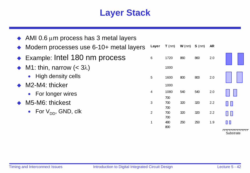
Layer Stack
AMI 0.6 μm process has 3 metal layersModern processes use 6-10+ metal layers
Example: Intel 180 nm processM1: thin, narrow (< 3λ)• High density cells
M2-M4: thicker• For longer wires
M5-M6: thickest• For VDD, GND, clk
Layer T (nm) W (nm) S (nm) AR
6 1720 860 860 2.0
1000
5 1600 800 800 2.0
1000
4 1080 540 540 2.0
7003 700 320 320 2.2
7002 700 320 320 2.2
7001 480 250 250 1.9
800
Substrate
Lecture 5 - 43Introduction to Digital Integrated Circuit DesignTiming and Interconnect Issues
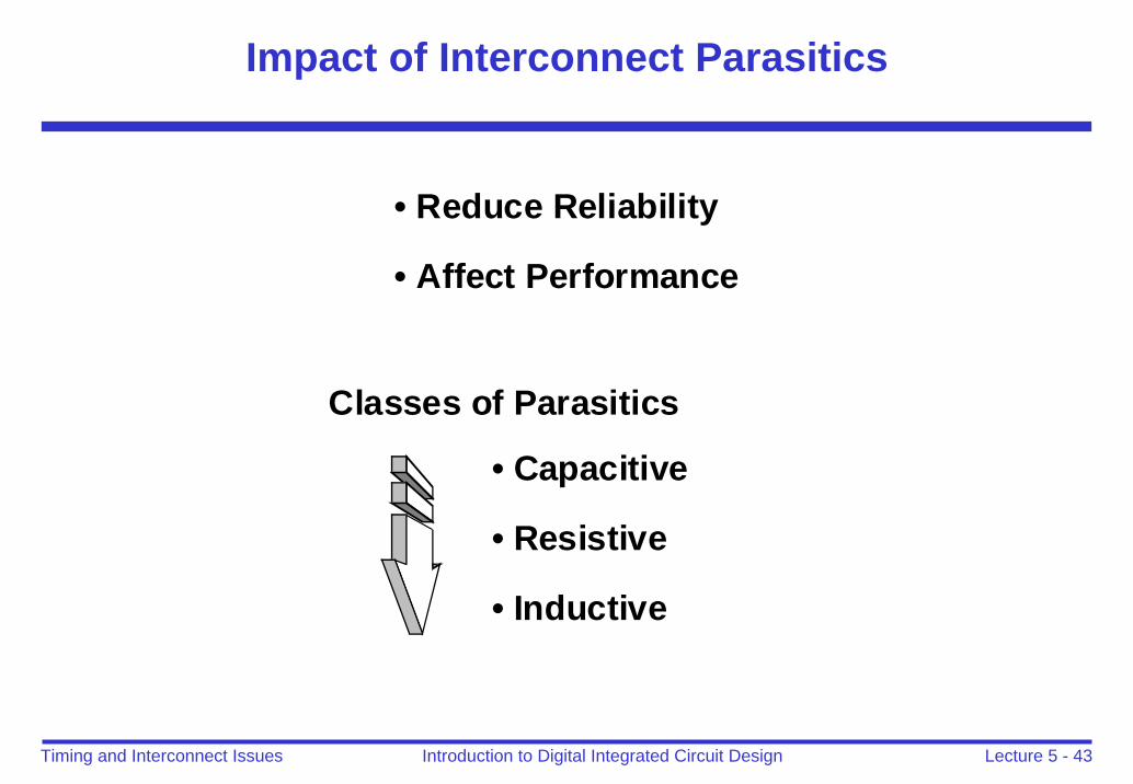
Impact of Interconnect Parasitics
• Reduce Reliability
• Affect Performance
Classes of Parasitics
• Capacitive
• Resistive
• Inductive

Lecture 5 - 44Introduction to Digital Integrated Circuit DesignTiming and Interconnect Issues
Wire Resistance
ρ = resistivity (Ω*m)R = sheet resistance (Ω/ )• is a dimensionless unit(!)
Count number of squares• R = R * (# of squares)
l lR Rt w wρ
= =
l
w
t
1 Rectangular BlockR = R (L/W) Ω
4 Rectangular BlocksR = R (2L/2W) Ω = R (L/W) Ω
t
l
w w
l
Lecture 5 - 45Introduction to Digital Integrated Circuit DesignTiming and Interconnect Issues
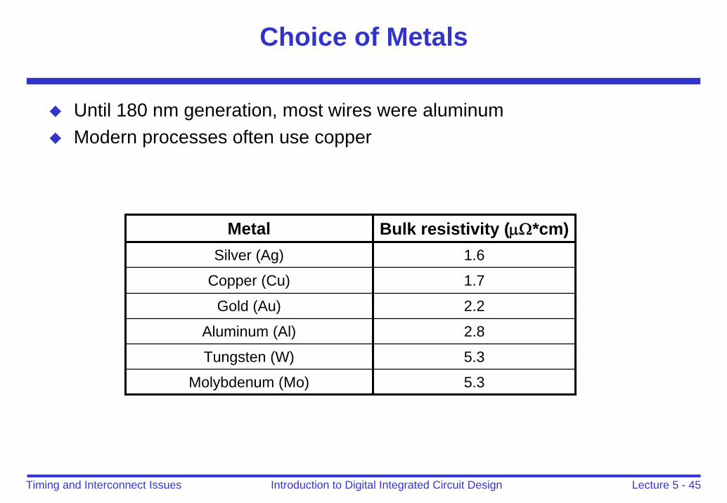
Choice of Metals
Until 180 nm generation, most wires were aluminumModern processes often use copper
Metal Bulk resistivity (μΩ*cm)Silver (Ag) 1.6
Copper (Cu) 1.7
Gold (Au) 2.2
Aluminum (Al) 2.8
Tungsten (W) 5.3
Molybdenum (Mo) 5.3

Lecture 5 - 46Introduction to Digital Integrated Circuit DesignTiming and Interconnect Issues
Sheet Resistance
Typical sheet resistances in 180 nm process
Layer Sheet Resistance (Ω/ )Diffusion (silicided) 3-10
Diffusion (no silicide) 50-200Polysilicon (silicided) 3-10
Polysilicon (no silicide) 50-400Metal1 0.08Metal2 0.05Metal3 0.05Metal4 0.03Metal5 0.02
Metal6 0.02
Lecture 5 - 47Introduction to Digital Integrated Circuit DesignTiming and Interconnect Issues
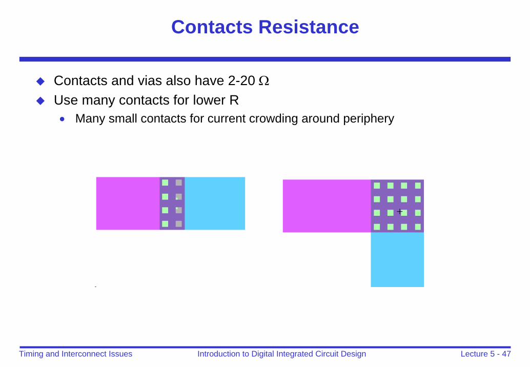
Contacts Resistance
Contacts and vias also have 2-20 ΩUse many contacts for lower R• Many small contacts for current crowding around periphery

Lecture 5 - 48Introduction to Digital Integrated Circuit DesignTiming and Interconnect Issues
Wire Capacitance
Wire has capacitance per unit length• To neighbors• To layers above and below
Ctotal = Ctop + Cbot + 2Cadj
layer n+1
layer n
layer n-1
Cadj
Ctop
Cbot
ws
t
h1
h2
Lecture 5 - 49Introduction to Digital Integrated Circuit DesignTiming and Interconnect Issues
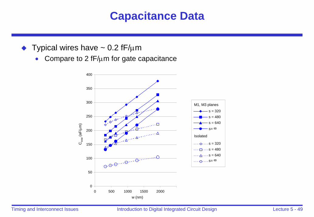
Capacitance Data
Typical wires have ~ 0.2 fF/μm• Compare to 2 fF/μm for gate capacitance
0
50
100
150
200
250
300
350
400
0 500 1000 1500 2000
Cto
tal (
aF/μ
m)
w (nm)
Isolated
M1, M3 planes
s = 320s = 480s = 640s= 8
s = 320s = 480s = 640
s= 8
Lecture 5 - 50Introduction to Digital Integrated Circuit DesignTiming and Interconnect Issues
Diffusion & Polysilicon
Diffusion capacitance is very high (about 2 fF/μm)• Comparable to gate capacitance• Diffusion also has high resistance• Avoid using diffusion runners for wires!
Polysilicon has lower C but high R• Use for transistor gates• Occasionally for very short wires between gates
Lecture 5 - 51Introduction to Digital Integrated Circuit DesignTiming and Interconnect Issues
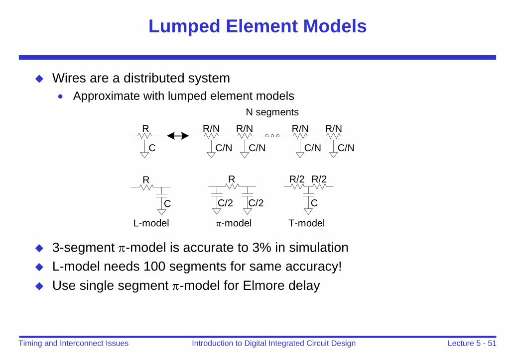
Lumped Element Models
Wires are a distributed system• Approximate with lumped element models
3-segment π-model is accurate to 3% in simulationL-model needs 100 segments for same accuracy!Use single segment π-model for Elmore delay
C
R
C/N
R/N
C/N
R/N
C/N
R/N
C/N
R/N
R
C
L-model
R
C/2 C/2
R/2 R/2
C
N segments
π-model T-model

Lecture 5 - 52Introduction to Digital Integrated Circuit DesignTiming and Interconnect Issues
Outline
Timing• Clocking• Self timed and asynchronous design• Synchronization
Interconnect• Wire geometry• Capacitance effects• Wire engineering

Lecture 5 - 53Introduction to Digital Integrated Circuit DesignTiming and Interconnect Issues
Capacitance Trends
Parallel plate equation: C = εA/d• Wires are not parallel plates, but obey trends• Increasing area (W, t) increases capacitance• Increasing distance (s, h) decreases capacitance
Dielectric constant• ε = kε0
ε0 = 8.85 x 10⁻¹⁴ F/cmk = 3.9 for SiO2
Processes are starting to use low-k dielectrics• k ≈ 3 (or less) as dielectrics use air pockets
Lecture 5 - 54Introduction to Digital Integrated Circuit DesignTiming and Interconnect Issues
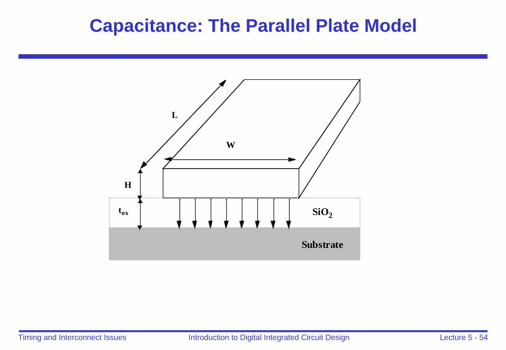
Capacitance: The Parallel Plate Model
SiO2
Substrate
L
W
H
tox

Lecture 5 - 55Introduction to Digital Integrated Circuit DesignTiming and Interconnect Issues
Typical Wiring Capacitance Values
Lecture 5 - 56Introduction to Digital Integrated Circuit DesignTiming and Interconnect Issues
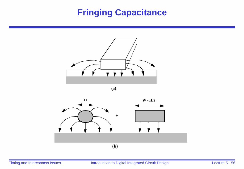
Fringing Capacitance
W - H/2H
+
(a)
(b)
Lecture 5 - 57Introduction to Digital Integrated Circuit DesignTiming and Interconnect Issues
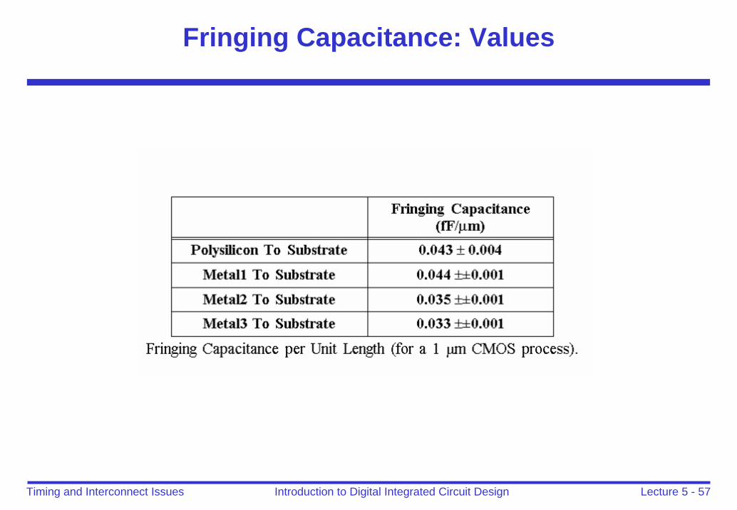
Fringing Capacitance: Values
Lecture 5 - 58Introduction to Digital Integrated Circuit DesignTiming and Interconnect Issues
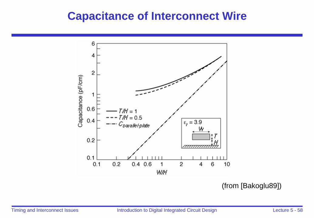
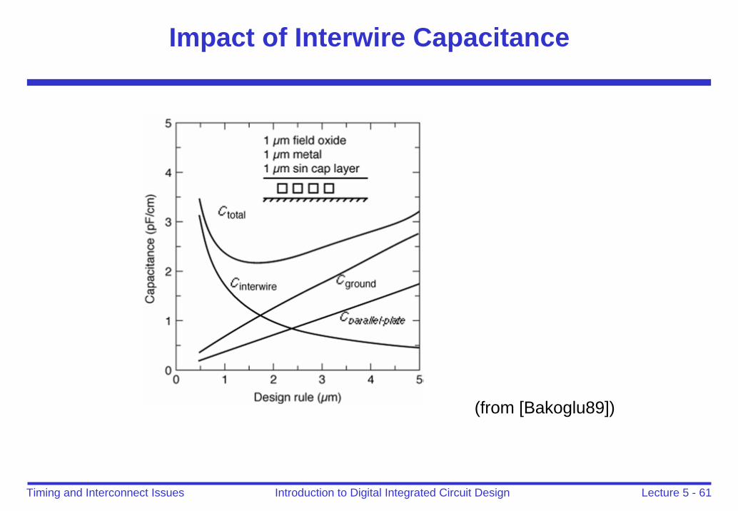
Capacitance of Interconnect Wire
(from [Bakoglu89])
Lecture 5 - 59Introduction to Digital Integrated Circuit DesignTiming and Interconnect Issues
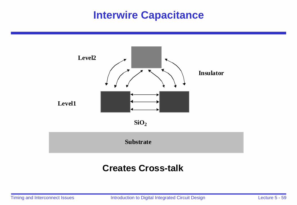
Interwire Capacitance
Substrate
SiO2
Insulator
Level1
Level2
Creates Cross-talk

Lecture 5 - 60Introduction to Digital Integrated Circuit DesignTiming and Interconnect Issues
Interwire Capacitance
Lecture 5 - 61Introduction to Digital Integrated Circuit DesignTiming and Interconnect Issues
Impact of Interwire Capacitance
(from [Bakoglu89])

Lecture 5 - 62Introduction to Digital Integrated Circuit DesignTiming and Interconnect Issues
Crosstalk
A wire has high capacitance to its neighbor.• When the neighbor switches from 1-> 0 or 0->1, the wire tends to switch too.• Called capacitive coupling or crosstalk.
Crosstalk effects• Noise on nonswitching wires• Increased delay on switching wires

Lecture 5 - 63Introduction to Digital Integrated Circuit DesignTiming and Interconnect Issues
Noise Implications
So what if we have noise?If the noise is less than the noise margin, nothing happensStatic CMOS logic will eventually settle to correct output even if disturbed by large noise spikes• But glitches cause extra delay• Also cause extra power from false transitions
Dynamic logic never recovers from glitchesMemories and other sensitive circuits also can produce the wrong answer

Lecture 5 - 64Introduction to Digital Integrated Circuit DesignTiming and Interconnect Issues
Capacitance Crosstalk
VDD
PDN
φ
In1
In2
In3
φ
CX
CXY
X
Y
5V
OV
5x5 μm Overlap: 0.35 V Interference
Lecture 5 - 65Introduction to Digital Integrated Circuit DesignTiming and Interconnect Issues
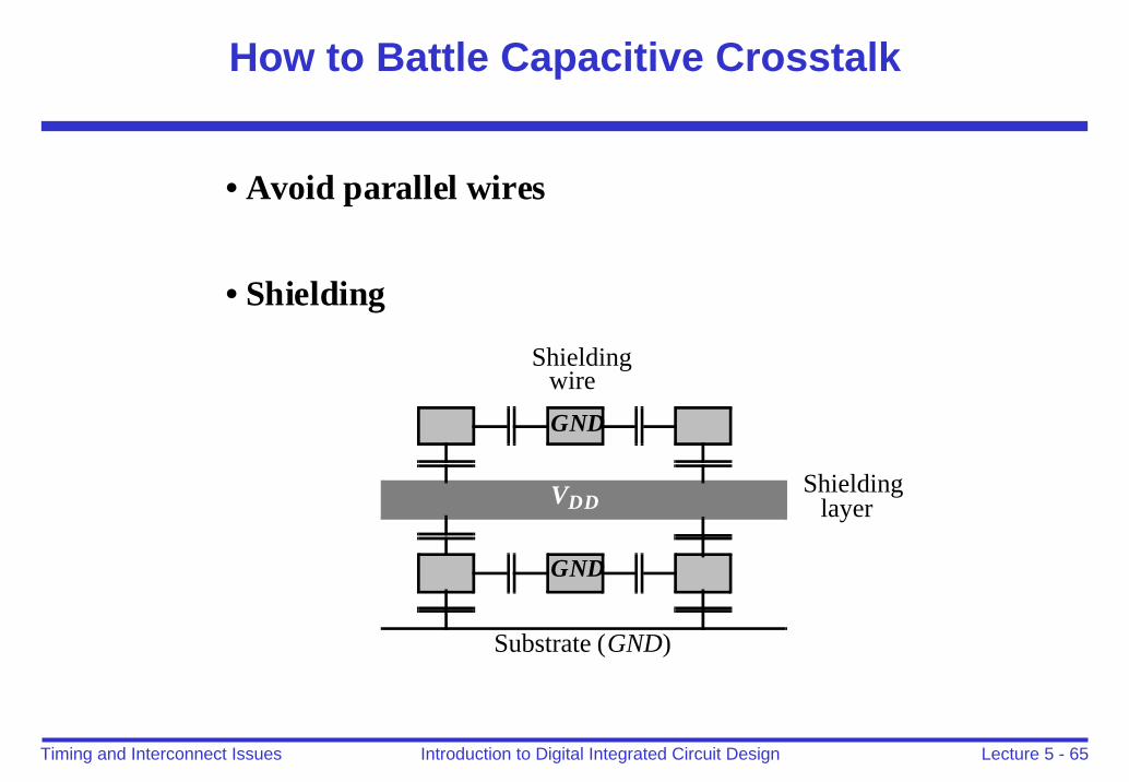
How to Battle Capacitive Crosstalk
Substrate (GND)
GND
ShieldinglayerVDD
GND
Shieldingwire
• Avoid parallel wires
• Shielding
Lecture 5 - 66Introduction to Digital Integrated Circuit DesignTiming and Interconnect Issues
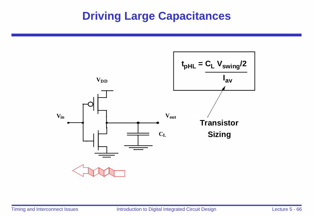
Driving Large Capacitances
VDD
Vin Vout
CL
tpHL = CL Vswing/2
Iav
TransistorSizing
Lecture 5 - 67Introduction to Digital Integrated Circuit DesignTiming and Interconnect Issues
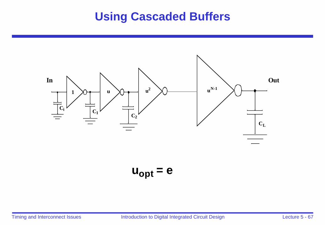
Using Cascaded Buffers
C2C1
Ci
CL
1 u u2 uN-1
In Out
uopt = e

Lecture 5 - 68Introduction to Digital Integrated Circuit DesignTiming and Interconnect Issues
Impact of Cascading Buffers
Lecture 5 - 69Introduction to Digital Integrated Circuit DesignTiming and Interconnect Issues
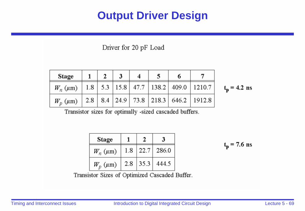
Output Driver Design
Lecture 5 - 70Introduction to Digital Integrated Circuit DesignTiming and Interconnect Issues
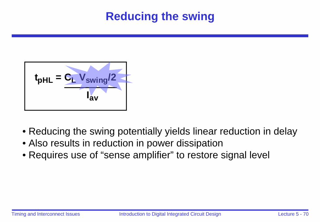
Reducing the swing
tpHL = CL Vswing/2
Iav
• Reducing the swing potentially yields linear reduction in delay• Also results in reduction in power dissipation• Requires use of “sense amplifier” to restore signal level
Lecture 5 - 71Introduction to Digital Integrated Circuit DesignTiming and Interconnect Issues
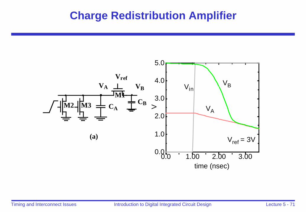
Charge Redistribution Amplifier
M1M2 M3
VrefVBVA
CBCA
(a)
0.0 1.00 2.00 3.00time (nsec)
0.0
1.0
2.0
3.0
4.0
5.0
V
VB
VA
Vin
Vref = 3V

Lecture 5 - 72Introduction to Digital Integrated Circuit DesignTiming and Interconnect Issues
Precharged Bus
In1.f
VDD
In2.fBus
CbusM1
M2
VDD
OutCoutM3
M4f
0 5 10t (nsec)-1.0
1.0
3.0
5.0V
Vbus
Vsym
f
Vasym
Cbus =1pF
Lecture 5 - 73Introduction to Digital Integrated Circuit DesignTiming and Interconnect Issues
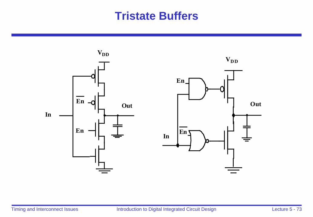
Tristate Buffers
In
VDD
En
EnOut
VDD
Out
In
En
En

Lecture 5 - 74Introduction to Digital Integrated Circuit DesignTiming and Interconnect Issues
Outline
Timing• Clocking• Self timed and asynchronous design• Synchronization
Interconnect• Wire geometry• Capacitance effects• Wire engineering

Lecture 5 - 75Introduction to Digital Integrated Circuit DesignTiming and Interconnect Issues
Wire Engineering
Goal: achieve delay, area, power goals with acceptable noiseDegrees of freedom:• Width • Spacing• Layer• Shielding
Del
ay (n
s): R
C/2
Wire Spacing(nm)
Cou
plin
g: 2C
adj /
(2C
adj+C
gnd)
00.20.40.6
0.81.01.21.4
1.61.82.0
0 500 1000 1500 20000
0.1
0.2
0.3
0.4
0.5
0.6
0.7
0.8
0 500 1000 1500 2000
320480640
Pitch (nm)Pitch (nm)
vdd a0a1gnd a2vdd b0 a1 a2 b2vdd a0 a1 gnd a2 a3 vdd gnd a0 b1

Lecture 5 - 76Introduction to Digital Integrated Circuit DesignTiming and Interconnect Issues
Repeaters
R and C are proportional to lRC delay is proportional to l2• Unacceptably great for long wires
Break long wires into N shorter segments• Drive each one with an inverter or buffer
Wire Length: l
Driver Receiver
l/N
Driver
Segment
Repeater
l/N
Repeater
l/N
ReceiverRepeater
N Segments

Lecture 5 - 77Introduction to Digital Integrated Circuit DesignTiming and Interconnect Issues
Repeater Design
How many repeaters should we use?How large should each one be?Equivalent Circuit• Wire length l
Wire Capacitance Cw*l, Resistance Rw*l• Inverter width W (nMOS = W, pMOS = 2W)
Gate Capacitance C’*W, Resistance R/W
R/W C'WCwl/2N Cwl/2N
RwlN


![Lect1 Introduction [호환 모드]tera.yonsei.ac.kr/class/2012_2_2/lecture/Introduction.pdf · Interconnect bottleneck ! (ITRS Roadmap 2009) Channel length: 250nm Interconnect delay](https://img.dokumen.tips/doc/110x75/5fb2865e51e929058d7518ca/lect1-introduction-eeoetera-interconnect-bottleneck-itrs-roadmap.jpg)